

SPT SPT7722SIT Datasheet
FEATURES
SPT7722
8-BIT, 250 MSPS ADC WITH DEMUXED OUTPUTS
PRELIMINARY INFORMATION
JULY 23, 2001
APPLICATIONS
• High conversion rate: 250 MSPS
• Single +5 V pow er supply
• Very low power dissipation: 450 mW
• 350 MHz full power bandwidth
• Po wer-down mode
• +3.0 V/+5.0 V (LVCMOS) digital output logic
compatibility
• Demuxed output ports
GENERAL DESCRIPTION
The SPT7722 is a high-speed, 8-bit analog-to-digital converter implemented in an advanced BiCMOS process. It is
a performance-enhanced version of the SPT7721, offering better linearity and dynamic performance with slightly
higher power . An adv anced folding and interpolating architecture provides both a high conversion r ate and very low
power dissipation of only 450 mW. The analog inputs can
be operated in either single-ended or differential input
mode. A 2.5 V common mode reference is provided on
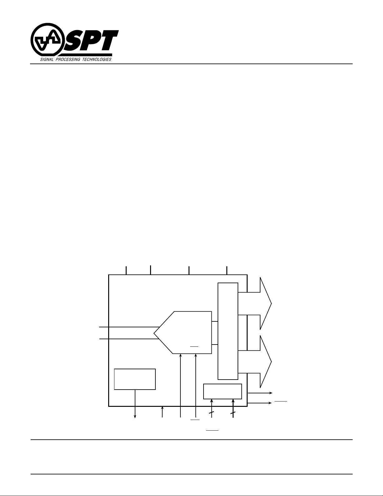
BLOCK DIAGRAM
AGND DGND
AV
• RGB video processing
• Digital communications
• High-speed instrumentation
• Digital sampling oscilloscopes (DSO)
• Projection display systems
chip for the single-ended input mode to minimize e xternal
components.
The SPT7722 digital outputs are demuxed (double-wide)
with both dual-channel and single-channel selectable output modes. Demuxed mode supports either parallel
aligned or interleaved data output. The output logic is both
+3.0 V and +5.0 V compatible. The SPT7722 is av ailable in
a 44-lead TQFP surf ace mount package ov er the industrial
temperature range of –40 to +85 °C.
CC
OV
DD
DA0DA
V
+
IN
8-Bit
7
250 MSPS
VIN
Common Mode
Voltage
Reference
+2.5 V
V
CM
PD CLK
ADC
CLK CLK
CLK
Data Output Latches
Data Output
Mode Control
22
Reset
DMODE
&
Reset
1,2
DB0DB
DCLK
OUT
DCLK
OUT
7
Signal Processing Technologies, Inc.
4755 Forge Road, Colorado Springs, Colorado 80907, USA
Phone: 719-528-2300 Fax: 719-528-2370 Web Site: http://www .spt.com e-mail: sales@spt.com

ABSOLUTE MAXIMUM RATINGS (Beyond which damage may occur)1 25 °C
Supply V oltages
AVCC...................................................................... +6 V
OVDD..................................................................... +6 V
Input V oltages
Analog Inputs ............................... –0.5 V to VCC +0.5 V
Digital Inputs ................................ –0.5 V to V
+0.5 V
CC
T emperatures
Operating Temperature........................... –40 to +85 °C
Storage Temperature ............................ –65 to +125 °C
Note: 1. Operation at any Absolute Maximum Rating is not implied.
See Electrical Specifications for nominal applied conditions in
typical applications.
ELECTRICAL SPECIFICATIONS
TA = T
PARAMETERS CONDITIONS LEVEL MIN TYP MAX UNITS
Resolution 8 Bits
DC Performance ƒIN=1 kHz
Analog Input
to T
, AV
MIN
MAX
= +5.0 V, OV
CC
= +5.0 V, ƒ
DD
= 250 MHz, unless otherwise specified.
CLK
TEST TEST SPT7722
Differential Linearity +25 °C I –0.6 ±0.4 +0.6 LSB
–40 °C to +85 °C V ±0.9 LSB
Integral Linearity +25 °C I –1.5 ±1.2 +1.5 LSB
Best Fit –40 °C to +85 °C V ±1.7 LSB
No Missing Codes @250 MSPS V Guaranteed
Input V oltage Range
(with respect to V
–) V ±512 mV
IN
Input Common Mode Voltage V 2.5 V
Input Bias Current V 5 µA
Input Resistance +25 °C V 50 kΩ
Input Capacitance +25 °C V 5 pF
Input Bandwidth +25 °C (–3 dB of FS) V 350 MHz
Gain Error V ±5 %
Offset Error V ±10 mV
P-P
Timing Characteristics
Conversion Rate V 250 MSPS
Output Delay (t
) +25 °C V 8 ns
pd1
Output Delay Tempco V 21 ps/°C
Aperture Delay Time (t
) V 0.5 ns
ap
Aperture Jitter Time V 2 ps rms
Pipeline Delay (Latency)
Single Channel Mode V 2.5 Clocks
Demuxed Interleaved Mode V 2.5 Clocks
Demuxed Parallel Mode
Channel B V 2.5 Clocks
Channel A V 3.5 Clocks
CLK to DCLK
Single Channel Mode (t
Dual Channel Mode (t
Delay Time
OUT
)V6ns
pd2
)V6ns
pd3
Dynamic Performance
Effective Number of Bits (ENOB)
= 70 MHz +25 °C I 6.3 7.0 Bits
ƒ
IN
= 70 MHz –40 °C to +85 °C V 5.9 Bits
ƒ
IN
Signal-to-Noise Ratio (SNR)
= 70 MHz +25 °C I 44 46 dB
ƒ
IN
ƒIN = 70 MHz –40 °C to +85 °C V 39 dB
SPT
SPT7722
2 7/23/01

ELECTRICAL SPECIFICATIONS
TA = T
MIN
to T
MAX
, AV
= +5.0 V, OVDD = +5.0 V, ƒ
CC
= 250 MHz, unless otherwise specified.
CLK
TEST TEST SPT7722
PARAMETERS CONDITIONS LEVEL MIN TYP MAX UNITS
Dynamic Performance
Total Harmonic Distortion (THD)
= 70 MHz +25 °C I –47 –43 dB
ƒ
IN
= 70 MHz –40 °C to +85 °C V –45 dB
ƒ
IN
Signal-to-Noise and Distortion (SINAD)
= 70 MHz +25 °C I 41 43 dB
ƒ
IN
= 70 MHz –40 °C to +85 °C V 41 dB
ƒ
IN
Power Supply Requirements
Voltage (Analog Supply) V 4.75 5.0 5.25 V
AV
CC
OVDD Voltage (Digital Supply) V 2.75 5.25 V
Current V 90 110 mA
AV
CC
Current Powerdown V 2.7 5 mA
AV
CC
Power Dissipation with Internal Voltage Reference V 450 5 50 mW
Power Supply Rejection Ratio V 35 mV/V
Common Mode Reference Output
Voltage V 2.45 2.5 2.55 V
Voltage Tempco V 119 ppm/°C
Output Impedance V 1 kΩ
Current Capability V 50 µA
Power Supply Rejection Ratio V 34 mV/V
Clock and Reset Inputs (Differential and Single-Ended)
Differential Signal Amplitude V
Differential High Input Voltage V
Differential Low Input Voltage V
DIFF
IHD
ILD
Differential Common-Mode Input V
Single-Ended High Input Voltage V
Single-Ended Low Input Voltage V
High Current Level V
Low Current Level V
<2.5 V V –100 20 +100 µA
ID
ID
CMD
IH
IL
V 400 mV
V 1.7 AV
V0 AV
CC
CC
–0.4 V
V
V 1.5 V
V 1.8 V
V 0 1.2 V
V –100 20 +100 µA
P-P
Power Down and Mode Control Inputs (Single-Ended)
High Input Voltage V 2 .0 AV
CC
V
Low Input Voltage V 0 1.0 V
Maximum Input Current Low V –100 10 +100 µA
Maximum Input Current High <4.0 V V –100 10 +100 µA
Digital Outputs
Logic "1" Voltage (I
Logic "0" Voltage (I
= –100 µA) V OVDD – 0.2 V
OH
= +100 µA) V 0.2 V
OL
TR/TF Data (10 pF load) V 3 ns
TR/TF DCLK = (10 pF load) V 1.5 ns
TEST LEVEL CODES
All electrical characteristics are subject to the
following conditions:
All parameters having min/max specifications
are guaranteed. The Test Level column indicates the specific device testing actually performed during production and Quality Assurance inspection. Any blank section in the data
column indicates that the specification is not
tested at the specified condition.
LEVEL TEST PROCEDURE
I 100% production tested at the specified temperature.
II 100% production tested at TA = +25 °C, and sample tested at the
specified temperatures.
III QA sample tested only at the specified temperatures.
IV Parameter is guaranteed (but not tested) by design and characteri-
zation data.
V Parameter is a typical value for information purposes only.
VI 100% production tested at TA = +25 °C. Parameter is guaranteed
over specified temperature range.
SPT
3 7/23/01
SPT7722
 Loading...