

SPT SPT674SIQ Datasheet
Signal Processing Technologies, Inc.
4755 Forge Road, Colorado Springs, Colorado 80907, USA
Phone: 719-528-2300 Fax: 719-528-2370 Web Site: http://www .spt.com e-mail: sales@spt.com
SPT7610
6-BIT, 1 GSPS FLASH A/D CONVERTER
FEATURES
• 1:2 demuxed ECL-compatible outputs
• 1.0 GSPS conversion rate
• Wide input bandwidth: 1.4 GHz
• Low input capacitance: 8 pF
• Metastable errors reduced to 1 LSB
• Monolithic construction
• Binary/Two’s complement output
APPLICATIONS
• Radar, EW, ECM
• Direct RF down-conversion
• Microwave modems
• Industrial ultrasound
• Transient capture
• Test and measurement
GENERAL DESCRIPTION
The SPT7610 is a full parallel (flash) analog-to-digital converter capable of digitizing full-scale (0 to –1 V) inputs into
six-bit digital words at an update rate of 1 GSPS. The
ECL-compatible outputs are demultiplexed into two separate output banks, each with differential data-ready outputs to ease the task of data capture. The SPT7610’ s wide
input bandwidth and low capacitance eliminate the need
for external track-and-hold amplifiers for most applications. A proprietary decoding scheme reduces metastable
errors to the 1 LSB level. The SPT7610 operates from a
single –5.2 V supply, with a nominal power dissipation of
2.75 W .
The SPT7610 is available in a 44L hermetic cerquad
surface-mount package in the industrial temperature
range (–40 °C to +85 °C).
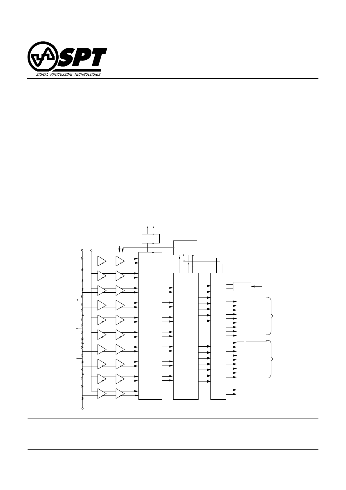
64
63
49
48
33
32
17
16
2
1
CLOCK
BUFFER
64 TO 6 BIT DECODER
WITH METASTABLE ERROR CORRECTION
DO
(LSB)
D1
D2
D3
D4
D5
(MSB)
D6
(OVR)
V
RT
Analog
Input
Preamp Comparator
V
RM
V
RB
CLKCLK
DEMUX
CLOCK
BUFFER
1:2 DEMULTIPLEXER
ECL OUTPUT BUFFERS AND LATCHES
DRB (DATA READY)
DRB (DATA READY)
D6B (OVR)
D5B (MSB)
D4B
D3B
D2B
D1B
D0B (LSB)
DRA (DATA READY)
DRA (DATA READY)
D6A (OVR)
D5A (MSB)
D4A
D3A
D2A
D1A
D0A (LSB)
D6B
D5B
D4B
D3B
D2B
D1B
D0B
D6A
D5A
D4A
D3A
D2A
D1A
D0A
BANK B
BANK A
V
R1
V
R3
MINV
LINV
TESTABILITY
TEST
BLOCK DIAGRAM

SPT
2 1/30/01
SPT7610
ABSOLUTE MAXIMUM RATINGS (Beyond which damage may occur)1 25 °C
Supply Voltages
Negative Supply Voltage (AVEE TO GND) .–7.0 to +0.5 V
Ground V oltage Differential........................–0.5 to +0.5 V
Input Voltage
Analog Input Voltage ................................+0.5 V to AV
EE
Reference Input Voltage ...........................+0.5 V to AV
EE
Digital Input Voltage.................................. +0.5 V to AV
EE
Reference Current VRT to VRB............................+20 mA
Note: 1. Operation at any Absolute Maximum Rating is not implied. See
Electrical Specifications for proper nominal applied conditions
in typical applications.
Output
Digital Output Current...................................0 to –25 mA
Temperature
Operating Temperature, Ambient............... –40 to +85 °C
Lead Temperature, (soldering 10 seconds) ........ +300 °C
Storage Temperature ............................... –65 to +150 °C
ELECTRICAL SPECIFICATIONS
TA = T
MIN
to T
MAX
, AV
EE
= –5.2 V , V
RB
= –1.00 V , V
RM
= –0.5 V , V
RT
= 0.00 V, ƒ
CLK
= 1000 MSPS, Duty Cycle = 50%, unless otherwise specified.
TEST TEST SPT7610
PARAMETERS CONDITIONS LEVEL MIN TYP MAX UNITS
Resolution 6 Bits
DC Accuracy
Integral Linearity VI –0.5 +0.5 LSB
Differential Linearity VI –0.5 +0.5 LSB
No missing codes VI Guaranteed
Analog Input
Offset Error V
RT
VI –30 +30 mV
Offset Error V
RB
VI –30 +30 mV
Input Voltage Range VI –1 0.0 Volts
Input Capacitance Over Full Input Range V 8 pF
Input Resistance V 50 kΩ
Input Bias Current VI 200 400 µA
Bandwidth Small Signal V 1.4 GHz
Input Slew Rate V 5 V/ns
Clock Synchronous Input Currents V 2 µA
Power Supply Requirements
Supply Current VI 550 770 mA
Power Dissipation VI 2.85 4.0 W
Reference Inputs
Ladder Resistance VI 60 80 120 Ω
Reference Bandwidth V 100 MHz
Digital Outputs
Digital Output High Voltage R
1
= 50 Ω to –2 V VI –1.2 –0.9 Volts
Digital Output Low Voltage R1 = 50 Ω to –2 V VI –1.8 –1.5 Volts
Digital Inputs
Digital Input High Voltage
(CLK, NCLK) VI –1.1 –0.7 Volts
Digital Input Low Voltage
(CLK, NCLK) VI –2.0 –1.5 Volts
Clock Input Swing
(CLK, NCLK) IV 100 700 mV
Maximum Sample Rate VI 1000 1200 MSPS
Clock Low Width, TPW0 VI 0.5 0.4 ns
Clock High Width, TPW1 VI 0.5 0.4 ns

SPT
3 1/30/01
SPT7610
ELECTRICAL SPECIFICATIONS
TA = T
MIN
to T
MAX
, AV
EE
= –5.2 V , V
RB
= –1.00 V , V
RM
= –0.5 V , V
RT
= 0.00 V, ƒ
CLK
= 1000 MSPS, Duty Cycle = 50%, unless otherwise specified.
TEST TEST SPT7610
PARAMETERS CONDITIONS LEVEL MIN TYP MAX UNITS
Timing Characteristics
Clock to Data Ready delay (t
dr
) +25 °C case V 950 ps
Clock to Output Data (t
od
) +25 °C case V 1.25 ns
Output Data to Data Ready (t
odr
) –40 to 85 °C case IV 550 750 950 ps
Output Data Skew (t
osk
) –40 to 85 °C case IV –150 150 ps
Aperture Jitter V 2 ps
Acquisition Time V 250 ps
Dynamic Performance
Spurious Free Dynamic Range (SFDR)
ƒ
IN
= 250 MHz V 45 dB
ƒ
IN
= 400 MHz V 34 dB
Signal-to-Noise and Distortion (SINAD)
ƒ
IN
= 250 MHz VI 31 34 dB
ƒ
IN
= 400 MHz VI 28 32 dB
Signal to Noise Ratio (SNR)
ƒ
IN
= 250 MHz VI 33 36 dB
ƒ
IN
= 400 MHz VI 32 36 dB
Total Harmonic Distortion (THD)
ƒ
IN
= 250 MHz VI –40 –37 dB
ƒ
IN
= 400 MHz VI –34 –30 dB
TEST LEVEL CODES
All electrical characteristics are subject to the
following conditions:
All parameters having min/max specifications
are guaranteed. The Test Level column indicates the specific device testing actually performed during production and Quality Assurance inspection. Any b lank section in the data
column indicates that the specification is not
tested at the specified condition.
Unless otherwise noted, all test are pulsed
tests; therefore, T
J
= TC = TA.
LEVEL TEST PROCEDURE
I 100% production tested at the specified temperature.
II 100% production tested at TA = +25 °C, and sample tested at the
specified temperatures.
III QA sample tested only at the specified temperatures.
IV Parameter is guaranteed (but not tested) by design and characteri-
zation data.
V Parameter is a typical value for information pur poses only.
VI 100% production tested at TA = +25 °C. Parameter is guaranteed
over specified temperature range.
 Loading...