SPT SPT5510SIM Datasheet

SPT5510
16-BIT, 200 MWPS ECL D/A CONVERTER
FEATURES
• 16-Bit, 200 MWPS digital-to-analog converter
• Differential linearity of ±0.6 LSB (typical)
• Integral linearity of ±0.75 LSB (typical)
• Fast settling time: 35 ns to 0.0008%; 25 ns to 0.01%
• Low glitch energy
• On-chip voltage reference
• ECL compatibility
GENERAL DESCRIPTION
The SPT5510 is a 16-bit, 200 MWPS digital-to-analog
converter designed for high-resolution waveform synthesis
for test and measurement instrumentation applications. It
features true 16-bit linearity, with differential non-linearity of
typically ±0.6 LSB and integral non-linearity of ±0.75 LSB. It
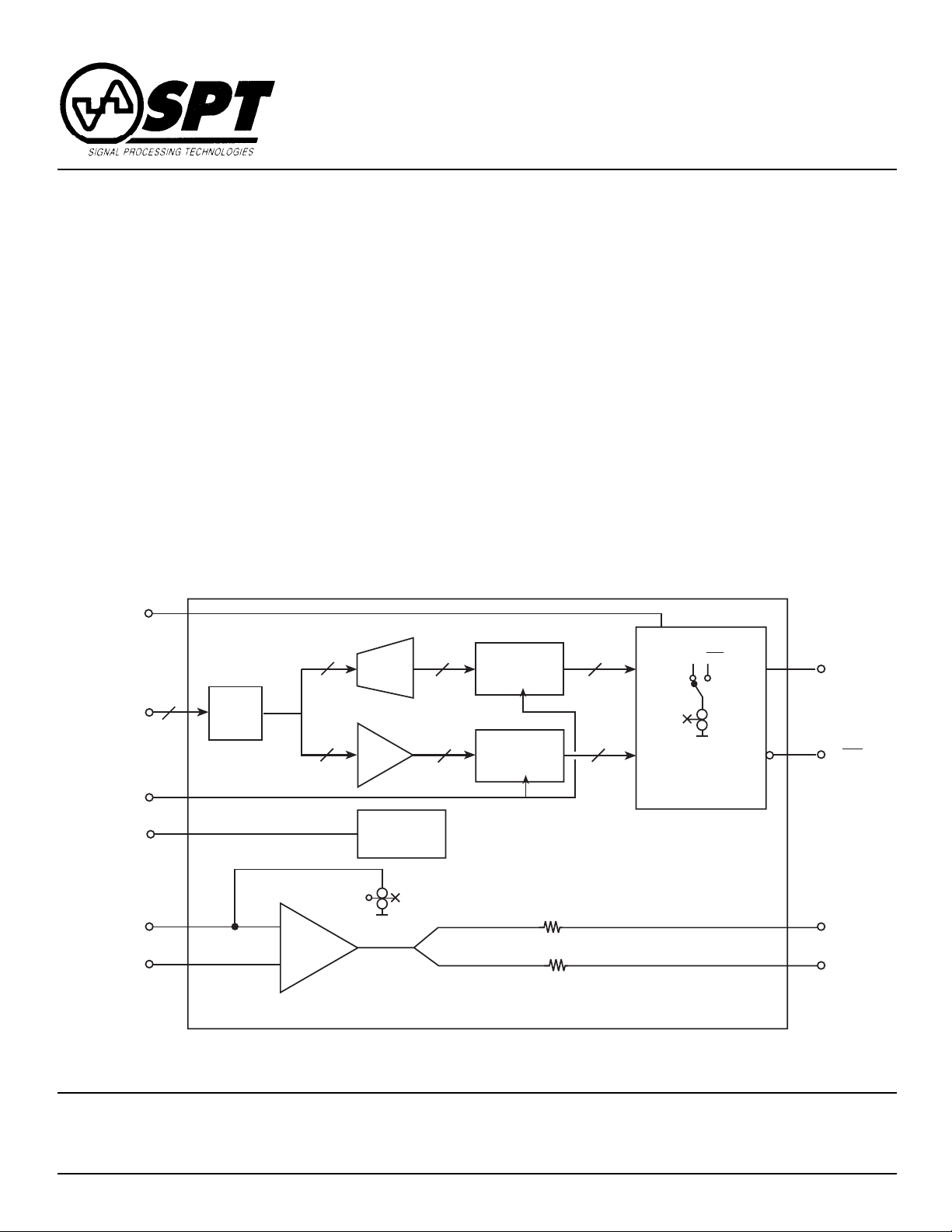
BLOCK DIAGRAM
REF
IN
D15–D12
MSB
Decoder
16 16
APPLICATIONS
• High-precision arbitrary waveform generation
• Test and measurement instrumentation
• Digital waveform synthesis
• Microwave and satellite modems
• Disk drive test equipment
• Industrial process control
• Military applications
has a very high-speed update rate of up to 200 MHz and is
ECL compatible. It has an ultrafast settling time of 25 ns to
0.01% and 35 ns to 0.0008%.
The SPT5510 operates over an industrial temperature
range of –40 °C to +85 °C and is available in a 10 x 10 mm,
44-lead metric quad flat pack (MQFP) plastic package.
I
I
OUT
MSB Latch
OUT
I
OUT
Digital Inputs
D15–D0
CLK
BG
OUT
R
SET
AMP
INB
Phone: (719) 528-2300 FAX: (719) 528-2370 Website: http://www.spt.com E-Mail: sales@spt.com
16
Input
Latch
D11–D0
+
Ref
Amp
–
LSB
Buffer
Bandgap
Reference
Reference
Cell
Bias
12
LSB Latch
Bias
12
Current
Cells
20
10
Signal Processing Technologies, Inc.
4755 Forge Road, Colorado Springs, Colorado 80907, USA
I
OUT
AMP
AMP
OUT
CC

ABSOLUTE MAXIMUM RATINGS (Beyond which damage may occur)
1
Supply Voltages
Negative supply voltage (VEE) .................................–7 V
A/D ground voltage differential................................0.5 V
Input Voltages
Digital input voltage (D15–D0, Clock)... ...........–2.5 to 0 V
Ref amp input voltage range..........................–2.5 to 0 V
Reference input voltage range (Ref In)...... V
to –2.5 V
EE
Output Currents
Bandgap reference output current .....................±500 µA
Ref amplifier output current................................ ±2.5 mA
Temperature
Operating temperature............................... –40 to +85 °C
Junction temperature .......................................... +150 °C
Lead, soldering (10 seconds) ............................. +250 °C
Storage ....................................................–65 to +150 °C
Note: 1. Operation at any Absolute Maximum Rating is not implied. See Electrical Specifications for nominal operating
conditions.
ELECTRICAL SPECIFICATIONS
TA= 25 °C, VEE=–5.2 V ±5%, 50% duty cycle clock, unless otherwise specified.
TEST TEST SPT5510
PARAMETERS CONDITIONS LEVEL MIN TYP MAX UNITS
DC Performance
Resolution 16 Bits
Differential Linearity VI –1.95 ±0.6 1.95 LSB
Differential Linearity T
Integral Linearity VI –1.95 ±0.75 1.95 LSB
Integral Linearity T
Integral Linearity Drift IV –0.2 0.2 LSB/°C
Offset Drift T
Monotonicity V 15 Bits
Output Capacitance V 10 pF
Gain Error I –2 0.4 2 % FS
Gain Error Tempco With Ext Reference V 50 ppm FS/°C
Gain Error Tempco With Internal Bandgap Ref V 50 ppm FS/°C
Offset Error I –4 4 µA
Compliance Voltage IV –1.2 2 V
Output Resistance IV 0.88 1.1 1.32 kΩ
Dynamic Performance
Conversion Rate IV 200 MHz
Settling Time t
Delay Time t
Glitch Energy V 30 pV-s
Full Scale Output Current With On-Chip References V 19 mA
Rise Time/Fall Time R
Spurious Free Dynamic Range
ƒ
=5 MHz; ƒ
OUT
ƒ
=10 MHz; ƒ
OUT
1
Measured at 0 V output using I-V.
2
Measured as voltage settling for mid-scale transition; RL = 50 Ω.
1
MIN–TMAX
MIN–TMAX
MIN–TMAX
2
ST
Settling to ±0.01% V 25 ns
Settling to ±0.0008% V 35 ns
D
= 50 Ω V2ns
L
=30 MHz 10 MHz Span V 84 dB
CLOCK
=100 MHz 10 MHz Span V 76 dB
CLOCK
IV –4.0 ±1.0 4.0 LSB
IV –4.0 ±1.5 4.0 LSB
IV –2.5 2.5 ppm FS/°C
V2ns
SPT
SPT5510
2 9/27/00

ELECTRICAL SPECIFICATIONS
TA= 25 °C, VEE=–5.2 V ±5%, 50% duty cycle clock, unless otherwise specified.
TEST TEST SPT5510
PARAMETERS CONDITIONS LEVEL MIN TYP MAX UNITS
Power Supply Requirements
Negative Supply Current (–5.2 V) T
Nominal Power Dissipation V 600 800 mW
Power Supply Rejection Ratio ∆V Supply = ±5 % I –0.6 ±0.002 0.6 % FS
Voltage Input and Control
Bandgap Reference Voltage V –1.2 V
Bandgap Output Current T
Ref Amp Bandwidth
3
Ref Amp Input Current V 16 µA
Ref Amp Output Current V 200 µA
Ref In Operating Voltage V –3.4 V
Digital Inputs
Logic 1 Voltage T
Logic 0 Voltage T
Logic 1 Current –0.8 V V 2.5 µA
Logic 0 Current –1.8 V V 0 µA
Input Capacitance V 3 pF
Input Setup Time (tS) IV 3.0 ns
Input Hold Time (t
Clock Pulse Width (t
3
Ref Amp Bandwidth is limited by its compensation network
) IV 0.5 ns
H
) IV 1.5 ns
PWH
–T
MIN
MAX
=25 °C ±10 °C IV –110 16 220 µA
A
VI 115 150 mA
V 40 MHz
MIN
MIN
–T
–T
MAX
MAX
VI –1.0 –0.8 V
VI –1.7 –1.5 V
TEST LEVEL CODES
All electrical characteristics are subject
to the following conditions:
All parameters having min/max specifications are guaranteed. The Test Level
column indicates the specific device
testing actually performed during production and Quality Assurance inspection. Any blank section in the data
column indicates that the specification
is not tested at the specified condition.
TEST LEVEL TEST PROCEDURE
I 100% production tested at the specified temperature.
II 100% production tested at TA = +25 °C, and sample tested at the specified
temperatures.
III QA sample tested only at the specified temperatures.
IV Parameter is guaranteed (but not tested) by design and characterization
data.
V Parameter is a typical value for information purposes only.
VI 100% production tested at T
specified temperature range.
= +25 °C. Parameter is guaranteed over
A
SPT
SPT5510
3 9/27/00
 Loading...