

SPT SPT5400SCP Datasheet
SPT
SIGNAL PROCESSING TECHNOLOGIES
SPT5400
13-BIT, OCTAL VOLTAGE-OUTPUT DAC
WITH PARALLEL INTERFACE
FEATURES
• Full 13-bit performance without external adjustments
• Eight DACs in one package
• Buffered voltage outputs
• Guaranteed monotonic to 13 bits
• Unipolar or bipolar output swing to ±4.5 V
• Output settling time of 7 µs to ±1/2 LSB
• Double-buffered digital inputs
DESCRIPTION
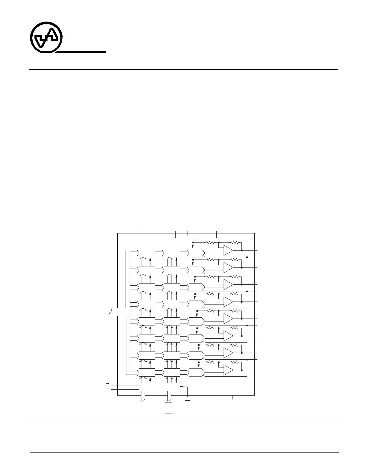
The SPT5400 has eight 13-bit voltage output digital-toanalog converters on one chip. It operates from ±5 V
power supplies and has maximum voltage output swings
of up to ±4.5 V without the addition of external components. Novel circuit topology allows for a guaranteed
monotonicity of 13 bits without the need for additional
circuitry. The SPT5400 has four separate reference voltage inputs, one for each pair of DACs. Four separate
BLOCK DIAGRAM
V
DD
INPUT
LATCH A
INPUT
LATCH B
REFAB REFCD
DAC
LATCH A
DAC
LATCH B
APPLICATIONS
• Automatic test equipment
• Flat-panel displays
• Arbitrary function generators
• Instrumentation
• Process control
analog ground pins allow for separate offset voltages for
each DAC pair. Each DAC can be asynchronously loaded
through a common 13-bit bus into a double-buffered set
of latches. All logic inputs are TTL/CMOS compatible.
The SPT5400 is available in a 44-lead PLCC package
over the commercial temperature range of 0 °C to
+70 °C.
REFEF REFGH
DAC A
DAC B
–
+
–
+
V
A
OUT
AGNDAB
B
V
OUT
D12–D0
CS
WR
DATA BUS
INPUT
LATCH C
INPUT
LATCH D
INPUT
LATCH E
INPUT
LATCH F
INPUT
LATCH G
INPUT
LATCH H
A0–A2 LDAB
CONTROL
LOGIC
LATCH C
LATCH D
LATCH E
LATCH F
LATCH G
LATCH H
LDCD
LDEF
LDGH
DAC
DAC
DAC
DAC
DAC
DAC
CLR
DAC C
DAC D
DAC E
DAC F
DAC G
DAC H
–
+
–
+
–
+
–
+
–
+
–
+
V
SS
GND
C
V
OUT
AGNDCD
D
V
OUT
E
V
OUT
AGNDEF
F
V
OUT
G
V
OUT
AGNDGH
H
V
OUT
Signal Processing Technologies, Inc.
4755 Forge Road, Colorado Springs, Colorado 80907, USA
Phone: (719) 528-2300 FAX: (719) 528-2370 Website: http://www.spt.com E-Mail: sales@spt.com

ABSOLUTE MAXIMUM RATINGS (Beyond which damage may occur)1 25 °C
Supply Voltages
VDD to GND............................................. –0.3 to +6 V
VSS to GND............................................. –6 to +0.3 V
AGNDxx..................... (GND – 0.3 V) to (VDD + 0.3 V)
Input Voltages
Digital Input Voltage to GND.. –0.3 V to (VDD + 0.3 V)
REFxx ..................(AGNDxx – 0.3 V) to (VDD + 0.3 V)
Maximum Current into REFxx Pin ................. ±10 mA
Note 1: Operation at any Absolute Maximum Rating is not implied. Operation beyond the ratings may cause damage to the
device. See Electrical Specifications for proper nominal applied conditions in typical applications.
Output
V
xx ...................................................... VDD to V
OUT
Temperature
Operating Temperature, Ambient..............0 to +70 °C
Junction Temperature ....................................+165 °C
Lead Temperature, (soldering 10 seconds) ...+300 °C
Storage Temperature ..........................–65 to +150 °C
Power Dissipation ....................................... 1000 mW
ELECTRICAL SPECIFICATIONS
VDD = +5 V, VSS = –5 V, REFxx = 4.096 V, AGNDxx = GND = 0 V, RL = 10 kΩ, CL = 50 pF, TA = T
specified. Typical values are at TA = +25 °C.
TEST TEST SPT5400
PARAMETERS CONDITIONS LEVEL MIN TYP MAX UNITS
DC Performance
Resolution 13 Bits
Integral Linearity VI ±0.5 ±4.0 LSB
Differential Linearity Guaranteed Monotonic VI ±1.0 LSB
Zero Code Error
Gain Error
Power Supply Rejection Ratio
∆Gain/∆V
∆Gain/∆V
1
2
3
DD
SS
Load Regulation R
= ∞ to 10 kΩ V ±0.4 LSB
L
VI ±10.0 ±20 LSB
VI ±1.0 ±15 LSB
VI ±0.0025 %/%
VI ±0.0025 %/%
Reference Input
Ref Input Range
4,5
Ref Input Resistance
5
IV AGND V
VI 5 kΩ
MIN
to T
, unless otherwise
MAX
DD
V
SS
Analog Output
Maximum Output Voltage V V
– 0.5 V
DD
Minimum Output Voltage V VSS + 0.5 V
Output Slew Rate V 2.4 V/µs
Output Settling Time
6
To ±1/2 LSB of Full Scale V 7.0 µs
Digital Feedthrough V 5 nV-s
Digital Crosstalk V 50 nV-s
Digital Inputs (VDD = 5 V ±5%)
Input Voltage High VI 2.4 V
Input Voltage Low VI 0.8 V
Input Current (V
= 0 V or VDD) VI 10.0 µA
IN
Input Capacitance IV 10 pF
Power Supplies
Positive Supply Range (V
Negative Supply Range (V
) VI 4.75 5.25 V
DD
) VI –5.25 –4.75 V
SS
Positive Supply Current VI 15 25 mA
Negative Supply Current VI 16 25 mA
Power Dissipation
1
Deviation of actual DAC output when all 0s are loaded to the DAC from the ideal output of –4.096 V.
2
Deviation of actual DAC output span from the ideal span of 8.191 V.
3
PSSR is tested by changing the respective supply voltage by ±5%.
4
For best performance, REF should be greater than AGND + 2 V and less than VDD – 0.6 V. The device operates
7
VI 155 250 mW
with reference inputs outside this range, but performance may degrade.
5
Reference input resistance is code dependent.
6
Typical settling time with 1000 pF capacitive load is 8 µs.
7
Does not include reference power.
SPT
2 5/15/00
SPT5400
TEST LEVEL CODES
All electrical characteristics are subject
to the following conditions:
All parameters having min/max specifications are guaranteed. The Test Level
column indicates the specific device
testing actually performed during production and Quality Assurance inspection. Any blank section in the data
column indicates that the specification
is not tested at the specified condition.
Figure 1 – Timing Diagram
CS
TEST LEVEL TEST PROCEDURE
I 100% production tested at the specified temperature.
II 100% production tested at TA = +25 °C, and sample tested at the
specified temperatures.
III QA sample tested only at the specified temperatures.
IV Parameter is guaranteed (but not tested) by design and characteriza-
tion data.
V Parameter is a typical value for information purposes only.
VI 100% production tested at T
specified temperature range.
t
1
= +25 °C. Parameter is guaranteed over
A
t
5
t
WR
t
9
2
A0–A2
t
7
D0–D12
LD
Table I – Timing Parameters
PARAMETER SYMBOL MIN TYP MAX UNIT
CS Pulse Width Low t
WR Pulse Width Low t
LD Pulse Width Low t
CLR Pulse Width Low t
CS to WR Low t
CS High to WR High t
Data Valid to WR Setup t
Data Valid to WR Hold t
Address Valid to WR Setup t
Address Valid to WR Hold t
1
2
3
4
5
6
7
8
9
10
50 ns
50 ns
50 ns
100 ns
0ns
0ns
20 ns
0ns
10 ns
0ns
t
6
t
10
t
8
NOTES:
1. All input rise and fall times
are measured from 10% to
90% of +5 V. tR = tF = 5 ns.
2. If LD is activated while WR is
low, LD must stay low for t3 or
t
4
t
3
longer after WR goes high.
SPT
SPT5400
3 5/15/00
 Loading...