SPT
SIGNAL PROCESSING TECHNOLOGIES
SPT5140
8-BIT, ULTRAHIGH-SPEED D/A CONVERTER
FEATURES
• 400 MWPS nominal conversion rate
• RS-343-A compatible
• Complete video controls: Sync, Blank, Bright
and Reference White (Force High)
• 10 KH, 100K ECL compatible
• Single power supply
• Registered data and video controls
• Differential current outputs
• Stable on-chip bandgap reference
• 50 and 75 ohm output drive
• ESD-protected data and control inputs
GENERAL DESCRIPTION
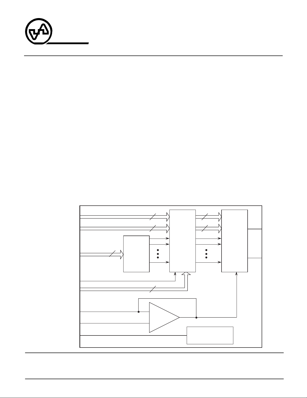
The SPT5140 is a monolithic 8-bit digital-to-analog converter capable of accepting video data at 400 MWPS.
Complete with video controls — Sync, Blank, Reference
White (Force High), Bright — the SPT5140 directly drives
doubly-terminated 50 or 75 ohm loads to standard composite video levels. Standard set-up level is 7.5 IRE. The
BLOCK DIAGRAM
APPLICATIONS
• Raster graphics
• High-resolution color or monochrome displays
to 2k x 2k pixels
• Medical electronics: CAT, PET, MR imaging displays
• CAD/CAE workstations
• Solids modeling
• General-purpose high-speed D/A conversion
• Digital synthesizers
• Automated test equipment
• Digital transmitters/modulators
SPT5140 includes an internal precision bandgap reference which can drive two other SPT5140s in an RGB
graphics system.
The SPT5140 is available in a 24-lead PDIP package in
the industrial temperature range of –25 °C to +85 °C.
Contact the factory for military temperature and /883
versions.
Video Controls In
Video Data In
Video Data In
Feedthrough
Convert
I
Set
Ref In
Ref Out
Sync, Blank, Bright, Ref – White
D0–D3
4 to 15
D4–D7
(MSBs)
4
Decode
4
4
2
Ref
Buffer
Register
4
4
Bandgap
Reference
Out +
Output
Current
Switches
Out –
Signal Processing Technologies, Inc.
4755 Forge Road, Colorado Springs, Colorado 80907, USA
Phone: (719) 528-2300 FAX: (719) 528-2370 Website: http://www.spt.com E-Mail: sales@spt.com

ABSOLUTE MAXIMUM RATINGS (Beyond which damage may occur)1 25 °C
Supply Voltages
VEE (measured to VCC) .......................... –7.0 to 0.5 V
Temperature
Operating,ambient............................... –25 to +85 °C
junction ....................................... + 175 °C
Input Voltages
CONV, Data, and Controls...................... VEE to 0.5 V
Lead, soldering (10 seconds) ...................... + 300 °C
Storage ............................................. –60 to + 150 °C
(measured to VCC)
Ref+ (measured to VCC) ......................... VEE to 0.5 V
Ref– (measured to VCC).......................... VEE to 0.5 V
Note 1: Operation at any Absolute Maximum Rating is not implied. See Electrical Specifications for proper nominal applied
conditions in typical applications.
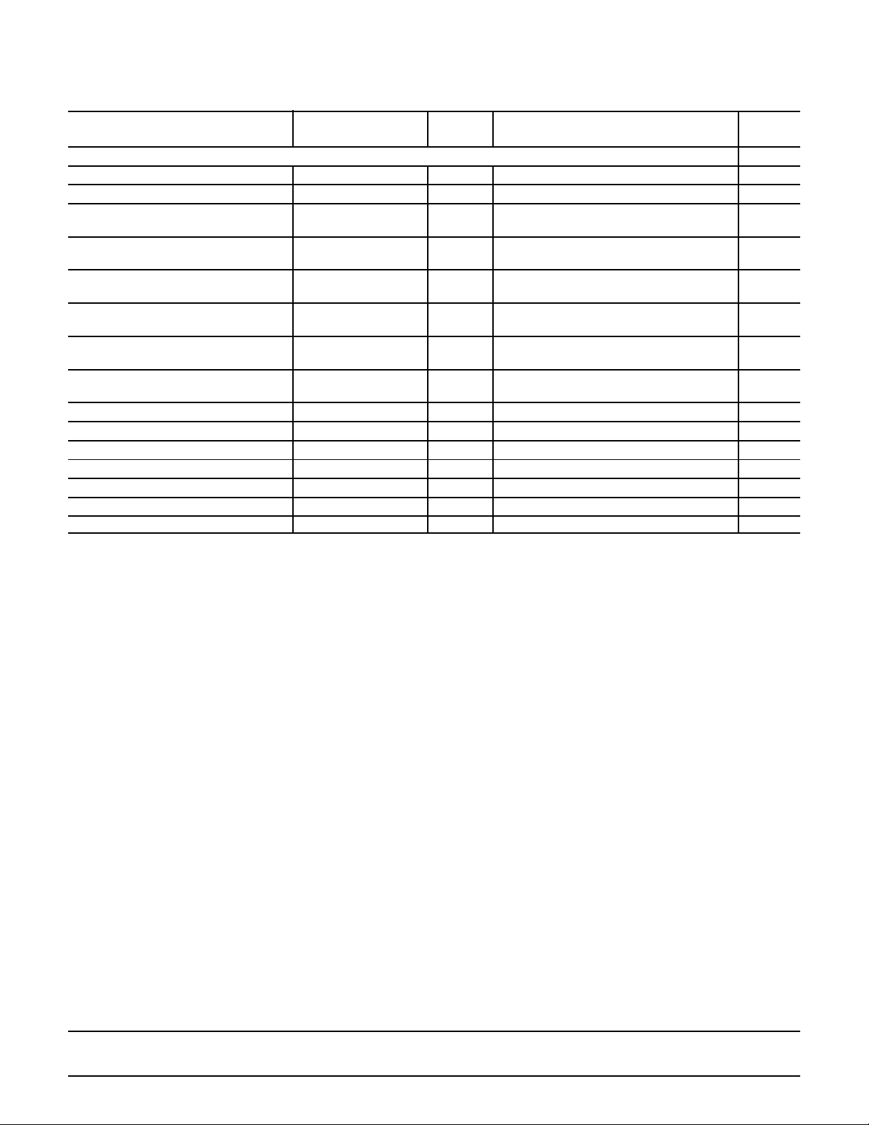
ELECTRICAL SPECIFICATIONS
VCC = ground, VEE = –5.2 V ±0.3 V, TA = T
PARAMETERS CONDITIONS LEVEL MIN TYP MAX UNITS
DC Electrical Characteristics
Integral Linearity Error 1.0 mA<I
Differential Linearity Error 1.0 mA<I
Gain Error VI –6.5 +6.5 % FS
Gain Error Tempco V 150 PPM/°C
Bandgap Tempco V 100 PPM/°C
Input Capacitance, I
Compliance Voltage, + Output VI –1.2 1.5 V
Compliance Voltage, – Output VI –1.2 1.5 V
Equivalent Output Resistance VI 20 kΩ
Output Capacitance V 9 pF
Maximum Current, + Output IV 45 mA
Maximum Current, – Output IV 45 mA
Output Offset Current VI 0.05 0.5 LSB
Input Voltage, Logic High VI –1.0 V
Input Voltage, Logic Low VI –1.5 V
Convert Voltage, IV –0.5 –2.5 V
Common Mode Range (V
Convert Voltage, Differential (V
Input Current, Logic Low, VI 35 120 µA
Data and Controls
Input Current, Logic High, VI 40 120 µA
Data and Controls
Input Current, Convert VI 2 60 µA
Reference Voltage
Measured to V
Reference Output Current VI –50 µA
Input Capacitance, V 3 pF
Data and Controls
Power Supply Sensitivity VI –120 +20 +120 µA/V
Supply Current VI 155 220 mA
, Ref Out V 5 pF
Set
)
ICM
) IV 0.4 1.2 V
IDF
CC
to T
MIN
TEST TEST SPT5140
, CC = 0 pF, I
MAX
<1.3 mA VI –0.37 +0.37 % FS
Set
<1.3 mA VI –0.2 +0.2 % FS
Set
= 1.105 mA, unless otherwise specified.
Set
–0.95 +0.95 LSB
–0.5 +0.5 LSB
VI –1.3 –1.2 –1.0 V
SPT
SPT5140
2 3/28/00

ELECTRICAL SPECIFICATIONS
VCC = ground, VEE = –5.2 V ±0.3 V, TA = T
PARAMETERS CONDITIONS LEVEL MIN TYP MAX UNITS
Dynamic Characteristics (RL = 37.5 ohms, CL = 5 pF, TA = +25 °C, I
Maximum Conversion Rate IV 385 400 MWPS
Rise Time 10% to 90% G.S. IV 900 ps
Rise Time 10% to 90% G.S. IV 600 ps
Current Settling Time, Clocked To 0.2% G.S. V 4 ns
Mode (t
)
SI
Current Settling Time, Clocked To 0.2% G.S. V 3 ns
Mode (t
)R
SI
Clock to Output Delay, Clocked IV 2.2 4 ns
Mode (t
) T
DSC
Part-to-Part Clock to Output Delay
Skew, Clocked Mode T
Data to Output Delay, IV 3.2 6 ns
Transparent Mode (t
) T
DST
Glitch Energy Area = 1/2 VT V 4 pV-s
Convert Pulse Width (t
PWH
, t
) IV 1.3 ns
PWL
Reference Bandwidth, –3 dB V 1.25 MHz
Set-up Time, Data and Controls (tS) IV 1.0 ns
Hold Time, Data and Controls (tH) IV 0.5 ns
Slew Rate 20% to 80% G.S. V 700 V/µS
Clock Feedthrough IV –48 dB
MIN
to T
, CC = 0 pF, I
MAX
Set
TEST TEST
Set
RL = 25 ohms
= 25 Ω
L
= T
A
A
A
= T
= T
MIN
MIN
MIN
to T
to T
to T
MAX
MAX
MAX
IV 4.5 ns
IV 1.5 ns
IV 6 ns
= 1.105 mA, unless otherwise specified.
= 1.105 mA)
TEST LEVEL CODES
All electrical characteristics are subject
to the following conditions:
All parameters having min/max specifications are guaranteed. The Test Level
column indicates the specific device
testing actually performed during production and Quality Assurance inspection. Any blank section in the data
column indicates that the specification
is not tested at the specified condition.
TEST LEVEL TEST PROCEDURE
I 100% production tested at the specified temperature.
II 100% production tested at TA = +25 °C, and sample tested at the
specified temperatures.
III QA sample tested only at the specified temperatures.
IV Parameter is guaranteed (but not tested) by design and characteriza-
tion data.
V Parameter is a typical value for information purposes only.
VI 100% production tested at T
specified temperature range.
= +25 °C. Parameter is guaranteed over
A
SPT
SPT5140
3 3/28/00

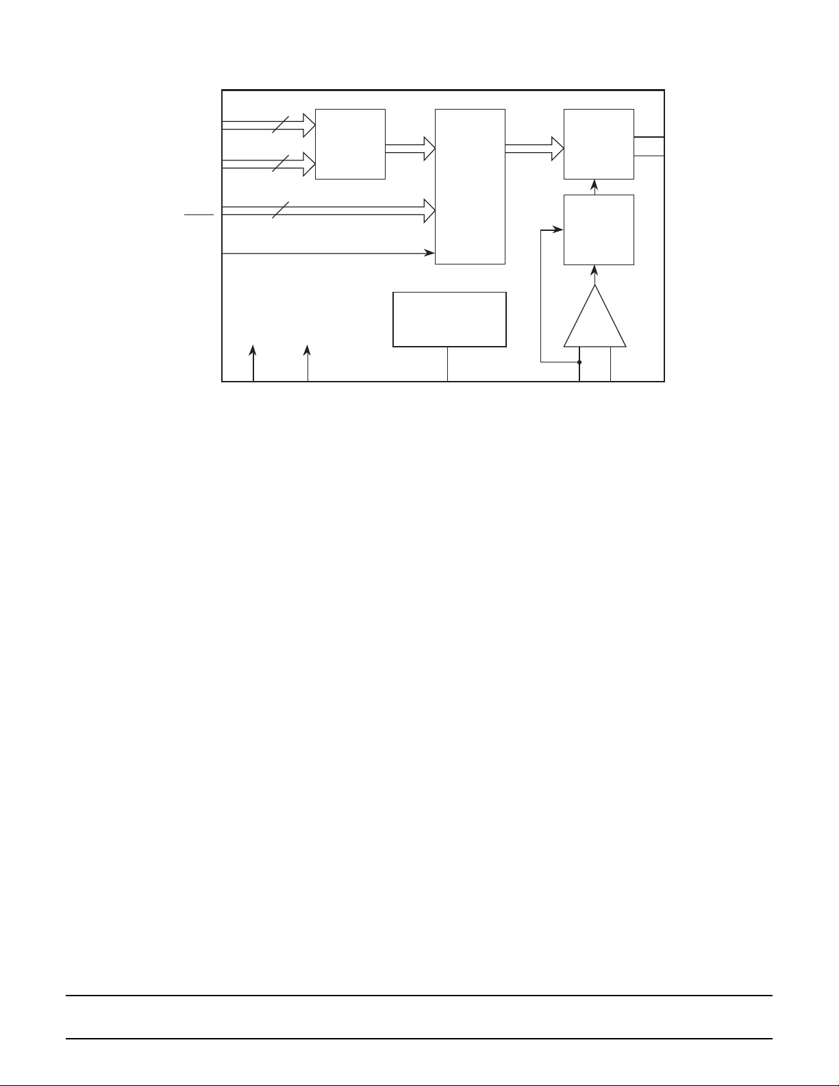
Figure 1 – Functional Diagram
D0–D7
Composite
Video Controls
CONV
CONV
Feedthrough
8
4
2
V
EE
V
CC
Decoding
Logic
APPLICATION INFORMATION
The SPT5140 is a high-speed video digital-to-analog
converter capable of up to 400 MWPS conversion rates.
This makes the devices suitable for driving 2048 X 2048
pixel displays at update rates of 60 to 90 Hz.
In addition, the SPT5140 includes an internal bandgap
reference which may be used to drive two other
SPT5140s if desired.
The SPT5140 has 10KH and 100K ECL logic level compatible video control and data inputs. The complementary
analog output currents produced by the devices are proportional to the product of the digital control and data
inputs in conjunction with the analog reference current.
The SPT5140 is segmented so that the four MSBs of the
input data are separated into a parallel “thermometer”
code. From here, fifteen current sinks, which are identical, are driven to fabricate sixteen coarse output levels.
The remaining four LSBs drive four binary weighted
current switches.
MSB currents are then summed with the LSBs that provide a one-sixteenth of full-scale contribution to provide
the 256 distinct analog output levels.
The video control inputs drive weighted current sinks
which are added to the output current to produce composite video output levels. These controls — Sync, Blank,
Reference White (Force High) and Bright — are needed
in video applications.
Another feature that similar video D/A converters do not
have is the Feedthrough Control. This pin allows registered or unregistered operation of the video control and
Data
Registers
Bandgap
Reference
Ref Out
Current
Sources
and
Switches
Current
Source
Biasing
Amp
+–
Ref In
I
Set
Out +
Out –
data inputs. In the registered mode, the composite functions are latched to the pixel data to prevent screen-edge
distortions generally found on unregistered video DACs.
TYPICAL INTERFACE CIRCUIT
GENERAL
A typical interface circuit using the SPT5140 in a color
raster application is shown in figure 2. The SPT5140
requires few external components and is extremely easy
to use. The very high operating speeds of the SPT5140
require good circuit layout, decoupling of supplies, and
proper design of transmission lines. The following considerations should be noted to achieve best performance.
INPUT CONSIDERATIONS
Video input data and controls may be directly connected
to the SPT5140. Note that all ECL inputs are terminated
as closely to the device as possible to reduce ringing,
crosstalk and reflections. A convenient and commonly
used microstrip impedance is about 130 ohms, which is
easily terminated using a 330 ohm resistor to VEE and a
220 ohm resistor to ground. This arrangement gives a
Thevenin equivalent termination of 130 ohms to –2 volts
without the need for a –2 volt supply. Standard SIP
(Single Inline Package) 220/330 resistor networks are
available for this purpose.
It is recommended that stripline or microstrip techniques
be used for all ECL interface. Printed circuit wiring
of known impedance over a solid ground plane is
recommended.
SPT
SPT5140
4 3/28/00
 Loading...