SPT SPT5100SCT Datasheet

SPT5100
8-BIT, 20 MWPS DUAL CHANNEL VIDEO DAC
Signal Processing Technologies, Inc.
4755 Forge Road, Colorado Springs, Colorado 80907, USA
Phone: (719) 528-2300 FAX: (719) 528-2370
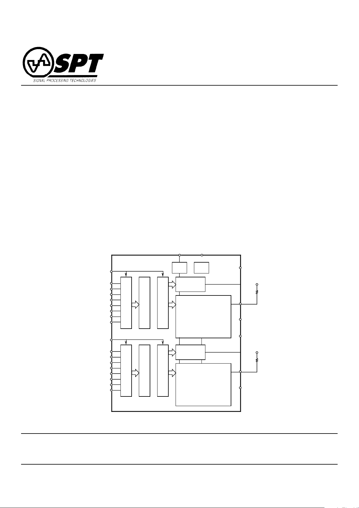
BLOCK DIAGRAM
FEATURES
• 8-Bit Dual Channel Video Digital-to-Analog Converter
• 20 MWPS Operation
• Low Power: 70 mW
• Internal Voltage Reference
• 5 V Monolithic CMOS
• 32-Lead QFP Package (7 mm by 7 mm, 0.8 mm Pitch)
APPLICATIONS
• High-speed Digital-to-Analog Conversion
• Y/ C, S-Video Processing
• Desktop Video Processing
• Digital TV
• Satellite TV Decoders
• Digital VCRs
current. The differential linearity errors of the DACs are
guaranteed to be a maximum of ±0.5 LSB over the full
temperature range. The device is available in a 32-lead QFP
package in the commercial temperature range.
GENERAL DESCRIPTION
The SPT5100 is an 8-bit, 20 MWPS, dual channel video digitalto-analog converter specifically designed for video processing applications including digital TV decoders and digital
VCRs. A single external resistor controls the full-scale output
Current
Swit ch Cell
Arr ay ( Ce ll 4)
V
CS
V
REF
C urr en t
Swit ch Cell
Arr ay ( Ce ll 4)
Current
Switch Cel l
Arr a y ( Cell 63)
Lat c h
Dec o der
Lat c h
Y
OU T
AV
DD
I
OY
(LSB) YØ
Y1
Y2
Y3
Y4
Y5
Y6
(MSB) Y7
CLKY
V
CS
V
REF
Current
Switch Cel l
Arr a y ( Cell 63)
Lat c h
Dec o der
Lat c h
C
OUT
AV
DD
I
OC
(LSB ) CØ
C1
C2
C3
C4
C5
C6
(MSB ) C7
CLKC
AV
SS
AV
SS
AV
DD
AV
DD

SPT
2 3/14/97
SPT5100
ELECTRICAL SPECIFICATIONS
f
CLK
= 20 MWPS, AVDD = 5.0 V, Output Pull-Up Load = 240 Ω, TA = 25 °C, AVSS = 0.0 V
TEST TEST
PARAMETERS CONDITIONS LEVEL MIN TYP MAX UNITS
DC ELECTRICAL CHARACTERISTICS
DC Performance
Resolution 8.0 Bits
Differential Linearity T
A
= T
MIN
to T
MAX
I ±0.25 ±0.5 LSB
Integral Linearity I ±0.5 ±1.0 LSB
Analog Outputs
Output Voltage Range VCS = +1.25 V I 4.0 5.0 V
Conversion Rate I 20 MWPS
Output Offset Voltage I 14 25 mV
Signal-to-Noise Ratio I 41 45 dB
Differential Phase V 1.2 Degrees
Differential Gain V 2 %
Glitch Energy V 80 pV-s
Settling Time I 31 26 ns
Propagation Delay (t
pd
) V 10 12 ns
Crosstalk I -47 dB
FS Control Voltage (VCS) IV 1.0 1.4 V
Digital Inputs and Timing
Input Current, Logic High VIH = 5 V I 5 µA
Logic Low V
IL
= 0 V I -5 µA
Set-Up Time, Data and Controls (t
S
)I5 ns
Hold Time, Data and Controls (t
h
) I 10 ns
Clock Pulse Width (Low) I 25 ns
Clock Pulse Width (High) I 25 ns
Power Supply Requirements
Supply Voltage I 4.75 5.25 V
Supply Current I 14 mA
Power Dissipation I 70 mW
ABSOLUTE MAXIMUM RATING (Beyond which damage may occur)
1
Supply Voltages
AV
DD
(measured to AVSS)........................... -0.3 to 7.0 V
Input Voltage
Clock and Data .........................................AVSS to AV
DD
Output Current
I
OUT
.............................................................................
0 to 8 mA
Temperature
Operating, ambient ........................................0 to +70 °C
Storage ....................................................-55 to + 125 °C
Note: 1. Operation at any Absolute Maximum Ratings is not implied. See Electrical Specifications for proper nominal applied
conditions in typical applications.
 Loading...