

SPT SPT2210SCT Datasheet
SPT
SIGNAL PROCESSING TECHNOLOGIES
SPT2210
Y/C VIDEO ENCODER
FEA TURES
• Supports NTSC (M) and PAL (B, D, G, H, I)
• CCIR 601, square pixel and 4Fsc operation
• 4:2:2 YCrCb and 4:1:1 YCrCb digital input formats
• Two on-chip 8-bit video DACs
• Internally generates SYNC and color burst signals
• Internal vertical interpolation filter
• Analog composite or Y/C output
• High-resolution mode supports Video CD, V2.0
• 16 CLUT RAM (programmable)
• Four modes of video/graphics operation:
graphics, video, chroma key and external key
• Color bar generation test function
• Suspend function
• 64-lead PQFP package
• Single +3.3 V power supply
GENERAL DESCRIPTION
The SPT2210 is a single-chip video encoder that is capable of converting digital video data (YCrCb) into analog
NTSC or P AL video signals. Two digital input formats are
supported: 4:2:2 (YCrCb) and 4:1:1 (YCrCb). It internally
generates the proper SYNC and color burst signals for
NTSC (525 lines/60 Hz) and P AL (625/50 Hz) video standards operating in any one of three sample rate modes:
CCIR 601, square pixel and 4Fsc.
Composite or Y/C S-Video analog video output is generated via two 8-bit internal video DACs. In addition, the
APPLICATIONS
• Video cameras
• Digital video tape recorders
• Video conference equipment
• Video frame grabbers
• Set-top boxes
• Video projection and displays
• Video printers
• Video game machines
• Multimedia PCs
SPT2210 supports external or chroma key functions for
color graphics pixel-by-pixel overlay. It has a 16-color
lookup-table overlay palette which is fully programmable.
It also has an on-chip vertical interpolation filter that can
be activated to reduce jaggy noise and flicker. The chip
also features an internal test color bar pattern generator.
The SPT2210 operates from a single +3.3 V supply and
is built in a 0.5 µm CMOS process. It is available in a 64lead PQFP package and operates over the commercial
temperature range.
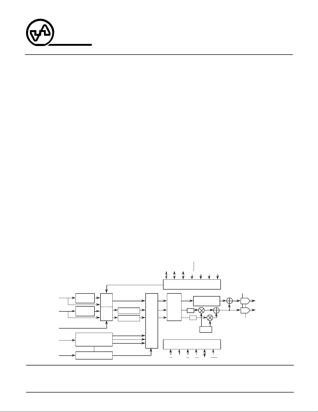
DTO
CBF
Suspend
V
CS
DAC
DAC
V
REF
BLOCK DIAGRAM
YD7…0
CD7…0
VRTENB
GD3…0
KEY
Vertical
Interpolation
Vertical
Interpolation
KEY Logic
CLUT
16 x 16
MUX
MUX
Interpolation
Interpolation
Y
Cr
Cb
Y
Cr
Cb
MUX
Field
H
Y
Level
Converter
Cr
Cb
CS RS RD WR D7…0 Reset
BLANK
V
SYNC Generator
Y
SYNC/BLANK
Cr
LPF
Cb
LPF
MPU Interface
CLK
Pedestal
Signal Processing Technologies, Inc.
4755 Forge Road, Colorado Springs, Colorado 80907, USA
Phone: (719) 528-2300 FAX: (719) 528-2370 Website: http://www.spt.com E-Mail: sales@spt.com
Y/CVBS
C

GENERAL DESCRIPTION OF FUNCTIONS
VIDEO MODES
The SPT2210 supports NTSC and PAL video standards
in Y/C (4:2:2) and Y/C (4:1:1) input formats. Table I shows
the video modes supported.
Table I – Supported Video Modes
Active Number Input Clock
Video Mode of Pixels Frequency
NTSC Square Pixel 640 x 483 12.2727 MHz
Y/C (4:2:2/4:1:1)
NTSC CCIR 601 720 x 483 13.5000 MHz
Y/C (4:2:2/4:1:1)
NTSC 4Fsc 768 x 483 14.3182 MHz
Y/C (4:2:2/4:1:1)
PAL Square Pixel 640 x 573 12.1875 MHz
Y/C (4:2:2/4:1:1)
PAL Square Pixel 768 x 573 14.7500 MHz
Y/C (4:2:2/4:1:1)
PAL CCIR 601 720 x 573 13.5000 MHz
Y/C (4:2:2/4:1:1)
PAL 4Fsc 948 x 573 17.7345 MHz
Y/C (4:2:2/4:1:1)
VERTICAL INTERPOLATION
The SPT2210 has a vertical interpolation filter that is
used to reduce jaggy noise and flicker. It also supports
the high-resolution mode for Video CD, version 2.0.
TWO-CHANNEL D/A CONVERTER OUTPUT
Digital video signals are output on two 8-bit D/A converters. Y/C (S-Video) output or composite video output can
be selected. The Y/C video outputs are current sources,
capable of driving a 75 Ω load to 1 V
ground. If both composite and S-Video are required simultaneously, a simple circuit (using the SPT9400 video
driver) may be added.
, referenced to
P-P
HOST INTERFACE
The operational modes and parameters of the SPT2210
can be changed via a MPU host parallel interface. The
following parameters can be changed:
• Low-pass filter
• Switching between Y/C output and composite output
• Switching between two’s complement or offset binary
data format
• Selecting between seven video modes
• 50%, Y, Y/C and color enable/disable
• Color bar test pattern
• Color kill (monochrome only out)
• Graphics mode control
• Software reset
• Select Y/C 4:2:2 or 4:1:1 input format
• Change of the Cr/Cb sampling order
• Interpolation field changeover
• Vertical interpolation filter bypass
• Free run or reset of subcarrier phase
• Turn off/on NTSC setup
• Suspend mode
• Input logic polarity set
• V Blank_ timing adjust
• H Blank_ timing adjust
EXTERNAL SETTING PINS
In addition to host interface control, the SPT2210 can be
operated independent of host interface using external pin
control. The external pin controls available are listed
below:
• Select between seven video modes
• Sync/Blank I/O mode
• Output of the built-in color bars
• Free run or reset of subcarrier phase
• Switching between Y/C output and composite output
• Turn off/on NTSC setup
See the External Setting Pin Descriptions section for
operation.
FOUR-BIT TITLE/GRAPHICS
MULTIPLEXING FUNCTION
Graphics from a 16-entry color lookup table can be arbitrarily displayed. In chroma mode it is possible to superimpose graphics and video input by specifying transparent colors. In the external key mode it is possible to
display graphics in the areas specified pixel by pixel.
SPT
SPT2210
2 8/22/00

Table II – Y/C Video Encoder Pin Functions
DESCRIPTION OF PIN FUNCTIONS
Signal Pin
Name Numbers I/O Function
Digital Video Inputs and Controls
YD7...0 1-8 I Luminance Digital Input
CD7...0 57-64 I Color Difference Digital Input
CBF 11 I Cr/Cb Sampling Order Control
BLANK_ 12 I External Blanking Control Signal
FIELD 16 I Field Indicator Signal (TTL Level)
V 13 I/O Vertical Synchronization Signal
H 14 I/O Horizontal Synchronization Signal
KEY 17 I Keying Signal Input (TTL Level)
GD3...0 18-21 I CLUT Ram Address (GD0 = LSB)
VRTENB 15 I Vertical Interpolation Enable
SUSPEND 43 I Suspend Mode Enable/Disable
Video Outputs
Y 53 O Luminance or Composite Video
C 49 O Chrominance Video Analog Signal
V
REF
V
CS
MPU Interface and Clock
D7...0 29-32,36-39 I/O Address/Data Bus (TTL Level)
CS_ 22 I Chip Select (TTL Level)
RS 23 I Register Select (TTL Level)
RD_ 24 I Read from Data Bus (TTL Level)
WR_ 25 I Write to Data Bus (TTL Level)
RESET_ 26 I Reset Signal Input (TTL Level)
CLK 34 I System Clock Input (Pixel Clock)
TEST 42 I Test Mode Enable/Disable
Power Supply Connections
VDD10,28,35,41,56 - +3.3 V Power Supply for Digital
AV
DD
GND 9,27,33,40,55 - Ground for Digital Circuitry
AGND 45,48,54 - Ground for Analog Circuitry
46 I Internal D/A Reference Voltage
47 I Internal D/A Output Signal
44,52 - +3.3 V Power Supply for Analog
(YD0 = LSB) (TTL Level)
(CD0 = LSB) (TTL Level)
(TTL Level)
Input (TTL Level)
Input (TTL Level)
Input (TTL Level)
(TTL Level)
(TTL Level)
Analog Signal Output (1 V
Output (1 V
Input
Amplitude Control Voltage
Circuitry
Circuitry
) (Includes burst)
P-P
P-P
)
DIGITAL VIDEO INPUTS AND CONTROLS
YD7...0 Pins
The luminance signal digital data is input on YD7...0 (TTL
level). The input can be in either offset binary or two’s
complement format. The range of the input data is
bounded from 16 to 235. Any data less than 16 is converted to 16 and data greater than 235 is converted to
235. The active pixels will be output after completion of
the back porch as shown in figure 2. YD7 is the MSB and
YD0 is the LSB.
CD7...0 Pins
The color difference digital data is input on CD7...0 (TTL
level). The input can be in either offset binary or two’s
complement format. The input range of the offset binary
mode is from 16 to 240, and the input range of the two’s
complement mode is from –112 to +112. Signal data is
bounded to these minimum and maximum limits.
As a means of dealing with abnormal data, color kill is
carried out when 00(H) of FF(H) is detected for two successive clocks or more at CD7...0 (automatic color kill
mode). Color kill is immediately cancelled when data
other than 00(H) or FF(H) are entered.
The order of Cr and Cb is determined by the combination
of the CBF pin (described below) and the Cr/Cb inversion
bit, D2 (data bit 2), of the command register CR1. In normal setup mode (Cr/Cb inversion bit = 0 and CBF pin = 1)
and 4:2:2 format, the input is started with the Cb data
and, after that, Cr and Cb are repeated alternately . (Refer
to figure 1.)
In the 4:1:1 format only (with normal CBF setup) the first
and the second data positions in time are used, and the
third and fourth data are ignored (or not present). (Refer
to figure 1.) The first data is repeated again after the
fourth data. The active pixels are output after the back
porch as shown in figure 2. CD7 is the MSB and CD0 is
the LSB.
CBF Pin
This is the Cr/Cb control pin. It determines the sampling
order of Cr/Cb. When the command register CR1, data
bit 2, (Cr/Cb inversion) is low (clear), the CBF pin is input
as positive true logic. (See the Command Register Descriptions.) When CBF is high, the SPT2210 samples the
data as Cb after the leading edge of HSYNC_ and the
back porch has occurred. When CBF is low, the SPT2210
samples the data as Cr after the leading edge of
HSYNC_ and the back porch has occurred.
When the command register CR1, data bit 2, (Cr/Cb Inversion) is high (set), the CBF pin is input as negative
logic. (See the Command Register Descriptions.) In this
mode the CBF pin is read as inverted.
SPT
SPT2210
3 8/22/00
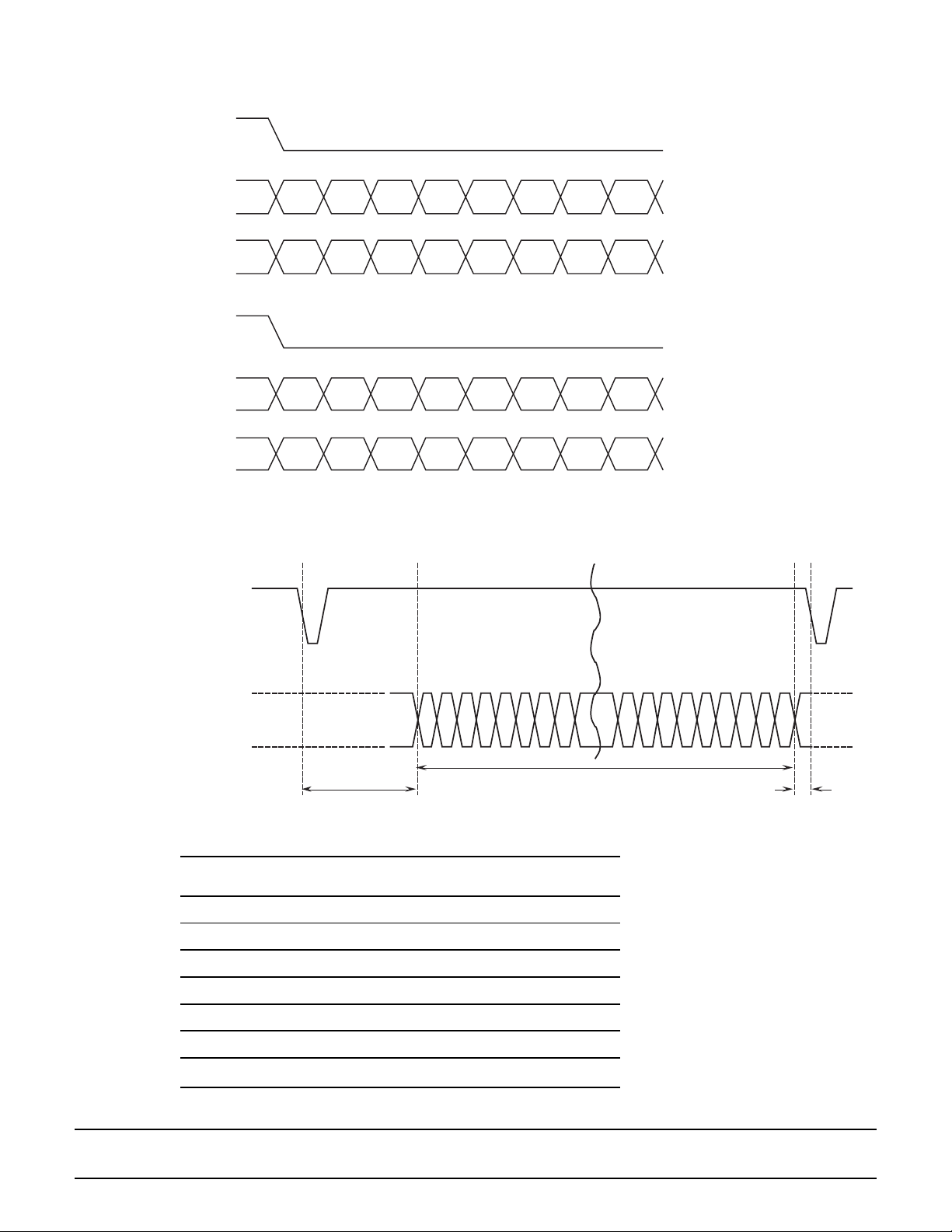
Figure 1 – Y/C Data Input Format (CBF=High, CR1:D2=0)
HSYNC_
YD7…0
CD7…0
HSYNC_
YD7…0
CD7…0
Y1 Y2 Y3 Y4 Y5 Y6 Y7
Cb1 Cr1 – – Cb5 Cr5 –
Y1 Y2 Y3 Y4 Y5 Y6 Y7
Cb1 Cr1 Cb5 Cr5
Figure 2 – Y/C Data Input Timing
HSYNC_
4:1:1 Format
Cb7Cb3 Cr3
4:2:2 Format
SPT
YD7…0
CD7…0
Effective Pixels
Back Porch Front Porch
Number of
Operation Mode Effective Pixels Back Porch Front Porch
NTSC CCIR 601 720 Clocks 122 Clocks 16 Clocks
NTSC Square Pixel 640 Clocks 120 Clocks 20 Clocks
NTSC 4Fsc 768 Clocks 124 Clocks 18 Clocks
PAL CCIR 601 720 Clocks 132 Clocks 12 Clocks
PAL Square Pixel (14.75) 768 Clocks 152 Clocks 24 Clocks
PAL 4Fsc 948 Clocks 164 Clocks 23 Clocks
PAL Square Pixel (12.18) 640 Clocks 120 Clocks 20 Clocks
SPT2210
4 8/22/00
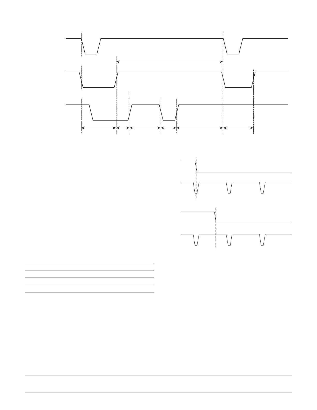
Figure 3 – Set of BLANK_ Terminal and Display/Nondisplay
HSYNC_
Internal Blank
Blank_
Nondisplay Non-
display
Display Non-
Blank_ Pin
This is the input pin for the external blanking control signal (TTL level). The SPT2210 samples BLANK_ at the
rising edge of CLK. When BLANK_ is high, the output
proceeds with normal operation and when it is low the
output signal gets blanked (i.e., no display). The specification of the blank state can be performed on a pixel-bypixel basis.
The chip has an internal blanking function that operates
independent of the external blanking signal. Figure 3
shows operation of the internal blanking in conjunction
with external blanking. Table III delineates the internal
blanking that is generated regardless of the level of the
blank pin, upon detection of HSYNC_.
Table III – Internal Blanking Periods for NTSC and
PAL
NTSC PAL
Lines 1 to 20 1 to 23
Lines 263 to 283 310 to 335
Line(s) 525 623 to 625
V Pin
This input pin provides the timing to generate the vertical
signal out of the SPT2210. The mode of operation for this
pin is controlled by Command Register, CR5. The sampling of the sync signal occurs on the rising edge of clock.
When the Vsync input signal is asserted during an Hsync
signal the field is considered to be odd, else the field is
even. (Refer to figure 4.)
display
Display Nondisplay
Figure 4 – Sync Signal Input Timing
VSYNC_
HSYNC_
Odd Numbered Field
VSYNC_
HSYNC_
Even Numbered Field
H Pin
This input pin provides the timing to generate the horizontal signal out of the SPT2210. The mode of operation for
this pin is controlled by Command Register, CR5. The
sampling of the sync signal occurs on the rising edge of
clock. When the timing for Hsync/Hblank input is different
from the number of clock cycles shown in table IV, the
phase of the subcarrier will be put into free-run.
Since the horizontal blanking period in Figure 2 is determined internally, the width and the trailing edge of
HSYNC_ are not detected. The active pixels are output
after the completion of the back porch as shown in
figure 2.
When in the blank operational mode the field is determined by the field input signal.
SPT
SPT2210
5 8/22/00

Table IV – Expected Line Clock Count for Various
Modes
Video Mode Clocks
NTSC 4Fsc 910
NTSC Square Pixel 780
NTSC CCIR 601 858
PAL 4Fsc 1135
PAL Square Pixel (ƒs = 14.75 MHz) 944
PAL Square Pixel (ƒs = 12.1875 MHz) 780
PAL CCIR 601 864
FIELD
This is an input signal controlled by CR5. It is sampled on
the leading edge of the clock cycle. It indicates the field
odd or even and is required in the Blank mode. High level
indicates ODD and low level indicates EVEN field.
TEST
This is an input signal. During normal operation it is set to
a logic low. Test functions of the device are enabled by
taking this pin to a logic high.
SUSPEND
This input pin is set to a logic low for normal operation.
When set to a logic high, the SPT2210 suspends operation and no output is active. This includes taking in data
from either the MPU data ports or video data.
KEY Pin
This is the external key input pin (TTL level). Input from
this pin is enabled when the external key mode is activated by setting the command register CR1 bits to D1 = 1
and D0 = 1. (See the Command Register Descriptions
section.) When KEY is high, the colors of the contents of
color lookup table (CLUT) that is specified by means of
GD3...0 are displayed. When KEY is low, the data of
YD7...0 and CD7...0 are output. This mode is called the
external key mode.
GD3...0 Pins
These are the graphic data input pins (TTL level). This
4-bit input port specifies which one of the 16 color entries
in the CLUT is to be output for the current pixel. If GD3...0
is all low when the SPT2210 is in chroma mode, the
CLUT output is transparent and the data of the YD7...0
and CD7...0 ports are output. (This assumes that the
transparent color was not changed in Address 0H of the
CLUT.) Refer to the Color Lookup Table (CLUT) Description section.
VRTENB Pin
This is the vertical interpolation enable signal input pin
(TTL level). When VRTENB is high, vertical interpolation
is enabled and when it is low, vertical interpolation is disabled.
N/C Pins
These are no connect pins.
VIDEO OUTPUTS
Y Pin
This is the luminance or composite analog output signal
pin. The Y output pin is a current source capable of driving a 75 Ω load terminated to ground to 1 V
. The en-
P-P
coded analog luminance or composite signal is output on
this pin.
C Pin
This is the chroma analog output signal pin. The C output
pin is a current source capable of driving a 75 Ω load
terminated to ground to 1 V
. The chroma signal is out-
P-P
put on this pin.
V
Pin
REF
This is the reference voltage input pin for the internal D/A
converters. A 0.1 µF capacitor and voltage divider of
6.8 kΩ and 5.1 kΩ resistors should be connected to this
pin from +3.3 V.
VCS Pin
This is the control voltage for the output amplitude of the
internal D/A converters. The D/A output amplitude can be
adjusted from 1.0 to 1.4 V
using this pin.
P-P
MPU INTERFACE AND CLOCK
D7...0 Pins
These are the address and data input/output bus pins
(TTL level). This is a bidirectional 8-bit bus. D7 is the
MSB and D0 is the LSB. When the CS_ (chip select) pin
is high, the D7...0 bus is in a high impedance state.
The SPT2210 features the ability to run without an external MPU host. In this mode, D7...0 and RS (Register
Select) pins can be used as external mode setting pins.
The D7...0 pins and RS pin become external setting pins
when CS_, RD_ (Read Enable) and WR_ (Write Enable)
are low for three clock cycles or more. Refer to the External Setting Pin Descriptions section for more details.
CS_ Pin
This is the chip select input pin (TTL level). The SPT2210
is selected for read/write operation when this pin is low.
The CS_ pin is also used in enabling the external pin
mode. Refer to the External Setting Pin Descriptions
section for more details.
SPT
SPT2210
6 8/22/00

RS_ Pin
This is the register select input pin (TTL level). The D7...0
pins operate as either address or data registers (except
when operating as external setting pins). The RS_ pin
determines the mode in which D7...0 will operate. When
RS_ is low the D7...0 bus is switched to the address bus
mode, and when it is high the bus is switched to the data
bus mode. The RS_ pin is also used as an external pin in
the external pin mode. Refer to the External Setting Pin
Descriptions section for more details.
RD_ Pin
This is the read enable input pin (TTL level). The data on
D7...0 is read out of the SPT2210 on the leading edge of
a high-to-low transition of RD_. If RS_ is high, the data is
read from the internal register specified by the last address write. If RS_ is low, the current address value is
read from the address register. The RD_ pin is also used
in enabling the external pin mode. Refer to the External
Setting Pin Descriptions section for more details.
WR_ Pin
This is the write enable input pin (TTL level). The data on
D7...0 is written into the address or command register on
the leading edge of a high-to-low transition of RD_. If RS_
is high, the data is written into the internal command register specified by the last address write. If RS_ is low, the
data is written into the address register. The WR_ pin is
also used in enabling the external pin mode. Refer to the
External Setting Pin Descriptions section for more
details.
AVDD Pins
These are the +3.3 V power supply pins for the analog
circuitry. VDD and AVDD are completely independent
of each other. Be sure to keep the following operating
condition:
| VDD – AVDD | ≤ 0.5 V.
GND Pins
These are the ground pins for the digital circuitry.
AGND Pins
These are the ground pins for the analog circuitry. Since
GND and AGND are completely independent of each
other, it is necessary to keep them at the same electric
potential by externally tying them together through a
ferrite bead.
Internal Pullup and Pulldown Resistors
The following pins are either pulled up or down with an
internal resistor of approximately 100 kΩ:
Pins with internal pulldown: CD7...0, YD7...0, GD3...0,
KEY, VRTENB, TEST, SUSPEND.
Pins with internal pullup: RESET_, BLANK_, V, H, CS_,
RD_, WR_, D7...0, CBF, RS, CLK.
Reset Pin
This is the reset input pin (TTL level). The reset input is
sampled on the leading edge of the system clock (CLK).
The SPT2210 is initialized by holding the RESET_ pin
low for a minimum of five clock cycles. The SPT2210 will
come out of reset five clock cycles after the RESET_ pin
has been brought back high.
CLK Pin
This is the system clock input pin (TTL level). The
YD7...0, CD7...0, GD3...0, BLANK_, V, H, Field and KEY
pins are all sampled on the rising edge of the CLK signal.
Additionally, when an asynchronous access from the
MPU is processed, the access is synchronized with this
clock and then the processing is carried out.
When the clock is switched over to another operating
frequency (i.e., changing video modes), the SPT2210
should be reset once to ensure proper operation. In this
case, the command registers will need to be set again.
VDD Pins
These are the +3.3 V power supply pins for the digital
circuitry.
SPT
SPT2210
7 8/22/00
 Loading...