SPT SPT205AIH, SPT205AMH Datasheet

Features
■
-3dB bandwidth of 170MHz
■
0.1% settling in 22ns
■
Complete overdrive protection
■
Low power: 570mW (190mW at ±5V)
■
3MΩ input resistance
■
Output may be current limited
■
Direct replacement for CLC205
Applications
■
Fast, precision A/D conversion
■
Automatic test equipment
■
Input/output amplifiers
■
Photodiode, CCD preamps
■
IF processors
■
High-speed modems, radios
■
Line drivers
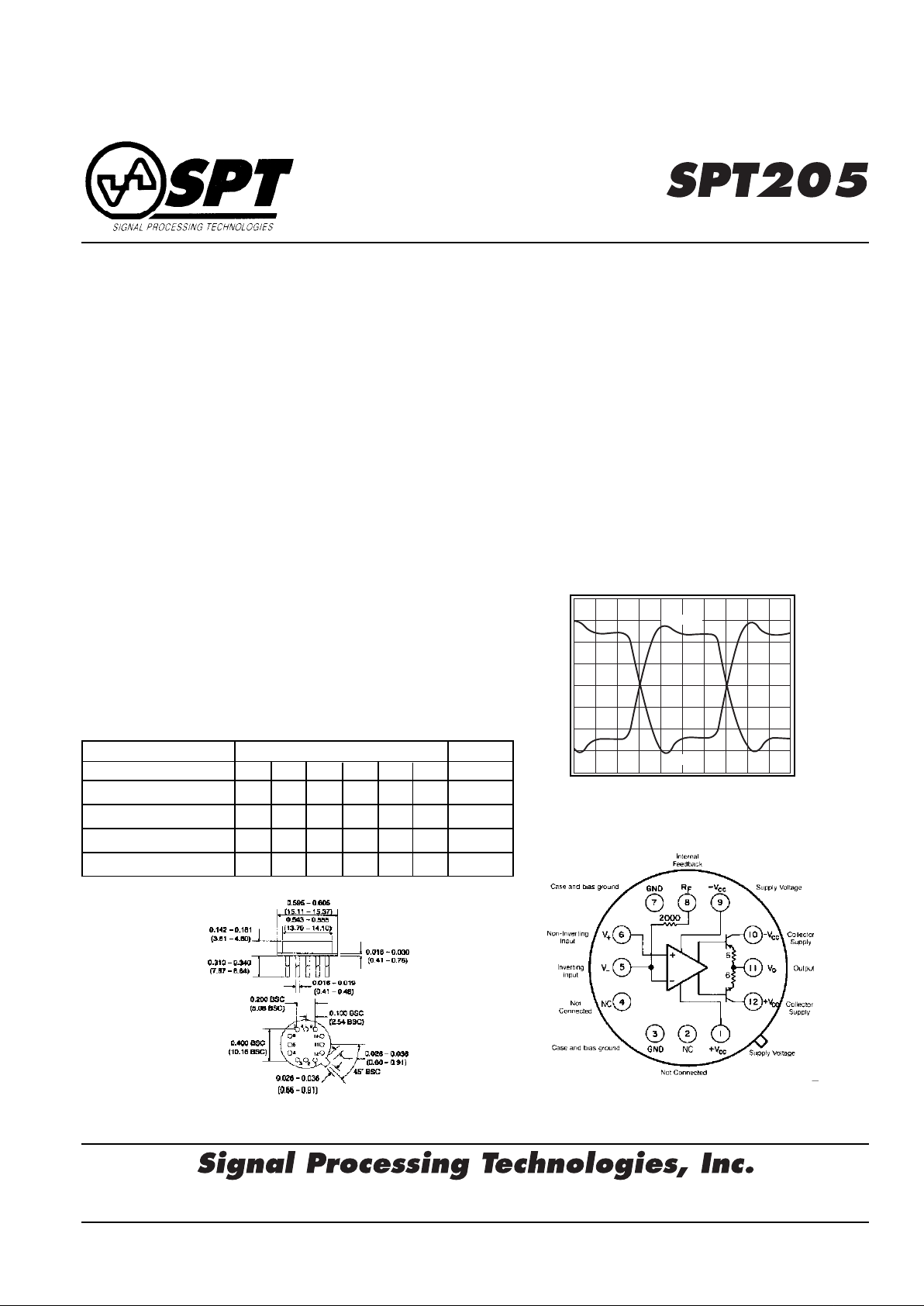
Bottom View
OVERDRIVE-PROTECTED WIDEBAND OP AMP
Package Dimensions
General Description
The SPT205 is a wideband overdrive-protected operational
amplifier designed for applications needing both speed and low
power operation. Utilizing a well-established current feedback
architecture, the SPT205 exhibits performance far beyond that
of conventional voltage feedback op amps. For example, the
SPT205 has a bandwidth of 170MHz at a gain of +20 and
settles to 0.1% in 22ns. Plus, the SPT205 has a combination of
important features not found in other high-speed op amps.
For example, the SPT205 has been designed to consume little
power – 570mW at ±15V supplies. The result is lower power
supply requirements and less system-level heat dissipation. In
addition, the device can be operated on supply voltages as low
as ±5V for even lower power dissipation.
Complete overdrive protection has been designed into the part.
This is critical for applications, such as ATE and instrumentation,
which require protection from signal levels high enough to cause
saturation of the amplifier. This feature allows the output of the
op amp to be protected against short circuits using techniques
developed for low-speed op amps. With this capability, even the
fastest signal sources can feature effective short circuit protection.
The SPT205 is constructed using thin film resistor/bipolar
transistor technology, and is available in the following versions:
SPT205AIH -25 to +85 °C 12-pin TO-8 can
SPT205AMH -55 to +125 °C 12-pin TO-8 can, features
burn-in and hermetic testing
4755 Forge Road, Colorado Springs, Colorado 80907, USA
Phone: (719) 528-2300 FAX: (719) 528-2370 Website: http://www.spt.com E-Mail: sales@spt.com
Typical Performance
Gain Setting
Parameter +7 +20 +50 -1 -20 -50 Units
Bandwidth (-3 dB) 220 170 80 220 130 80 MHz
Rise time 1.7 2.2 4.7 1.7 2.9 4.7 ns
Slew Rate 2.4 2.4 2.4 2.4 2.4 2.4 V/ns
Settling Time (to 0.1%) 22 22 20 21 20 19 ns
Large Signal Pulse Response
Output Voltage (2V/div)
Time (5ns/div)
205 Plot8
Av = +20
Av = -20

2 10/9/98
SPT205
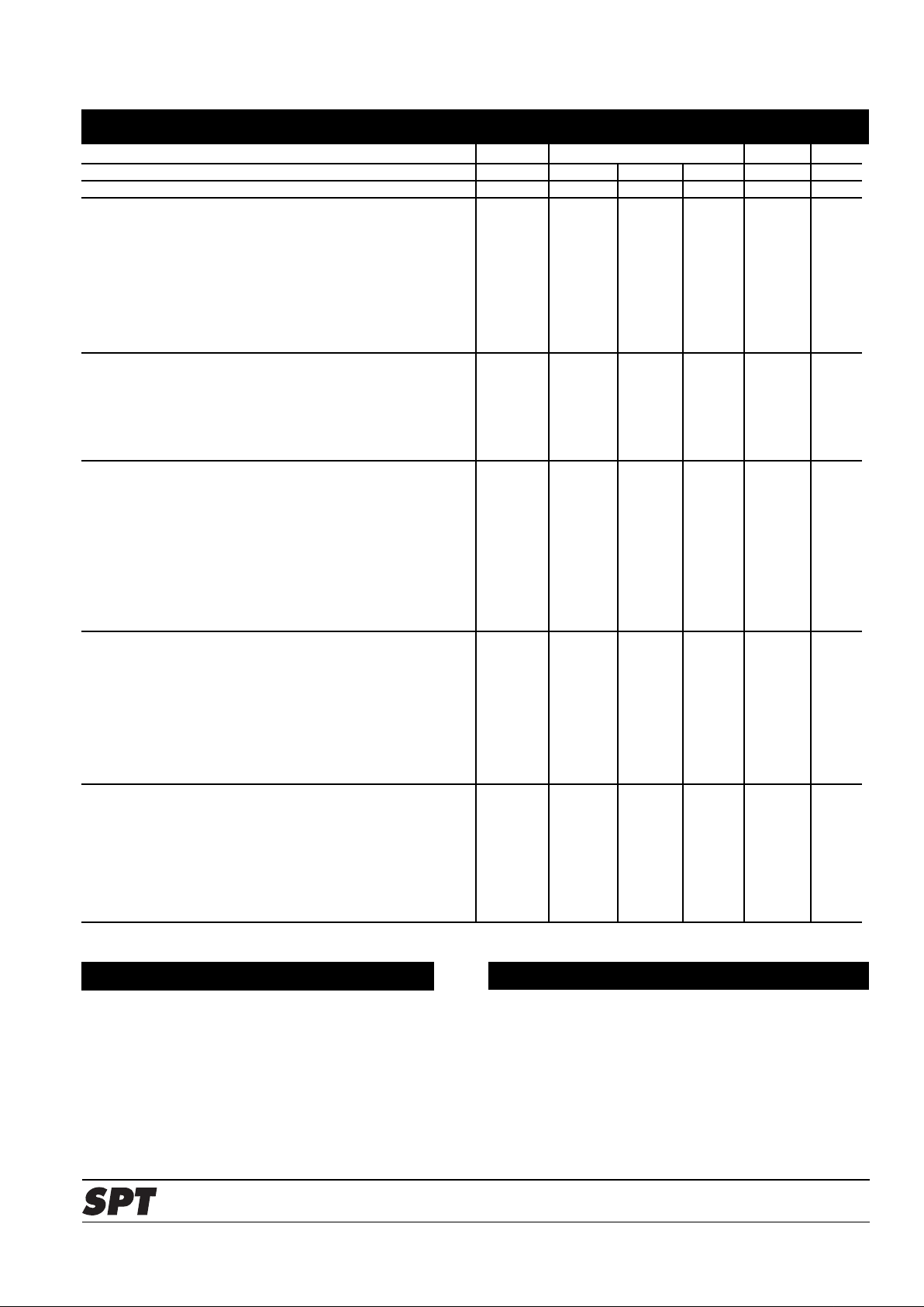
PARAMETERS CONDITIONS TYP MIN & MAX RATINGS UNITS SYM
Ambient Temperature SPT205AIH +25°C -25°C +25°C +85°C
Ambient Temperature SPT205AMH +25°C -25°C +25°C +85°C
FREQUENCY DOMAIN RESPONSE
✝ -3dB bandwidth V
o
= <2V
pp
170 >140 >140 >125 MHz SSBW
large-signal bandwidth V
o
= <10V
pp
100 >72 >80 >80 MHz FPBW
gain flatness V
o
= <2V
pp
✝ peaking 0.1 to 35MHz 0 <0.3 <0.3 <0.5 dB GFPL
✝ peaking >35MHz 0 <0.5 <0.5 <0.8 dB GFPH
✝ rolloff at 70MHz – <0.8 <0.8 <0.8 dB GFR
group delay to 70MHz 3.0 ± .2 – – – ns GD
linear phase deviation to 70MHz 0.8 <3.0 <2.0 <3.0 ° LPD
TIME DOMAIN RESPONSE
rise and fall time 2V step 2.2 <2.6 <2.6 <3.0 ns TRS
10V step 4.8 <5.5 <5.5 <5.5 ns TRL
settling time to 0.1% 10V step, note 2 22 <27 <27 <27 ns TS
to 0.05% 10V step, note 2 24 <30 <30 <30 ns TSP
overshoot 5V step 7 <14 <14 <14 % OS
slew rate 20Vpp at 50MHz 2.4 >1.8 >2.0 >2.0 V/ns SR
NOISE AND DISTORTION RESPONSE
✝ 2nd harmonic distortion 2V
pp
, 20MHz -57 <-50 <-50 <-50 dBc HD2
✝ 3rd harmonic distortion 2V
pp
, 20MHz -68 <-55 <-55 <-55 dBc HD3
equivalent input noise
voltage >100kHz 2.1 <3.0 <3.0 <3.5 nV/√Hz VN
inverting current >100kHz 22 <30 <30 <35 pA/√Hz ICN
non-inverting current >100kHz 4.8 <6.5 <6.5 <7.5 pA/√Hz NCN
noise floor >100kHz -157 <-154 <-154 <-153 dBm(1Hz) SNF
integrated noise 1kHz to 150MHz 39 <55 <55 <61 µV INV
noise floor >5MHz -157 <-154 <-154 <-153 dBm(1Hz) SNF
integrated noise 5MHz to 150MHz 39 <55 <55 <61 µV INV
STATIC, DC PERFORMANCE
* input offset voltage 3.5 <8.0 <8.0 <11.0 mV VIO
average temperature coefficient 11 <25 <25 <25 µV/°C DVIO
* input bias current non-inverting 3.0 <25 <15 <15 µΑ IBN
average temperature coefficient 15 <100 <100 <100 nA/°C DIBN
* input bias current inverting 2.0 <22 <10 <25 µA IBI
average temperature coefficient 20 <150 <150 <150 nA/°C DIBI
* power supply rejection ratio 69 >55 >55 >55 dB PSRR
common mode rejection ratio 60 >50 >50 >50 dB CMRR
* supply current no load 19 <20 <20 <22 mA ICC
MISCELLANEOUS PERFORMANCE
non-inverting input resistance DC 3.0 >1.0 >1.0 >1.0 MΩ RIN
non-inverting input capacitance 70MHz 5.0 <7.0 <7.0 <7.0 pF CIN
output impedance DC – <0.1 <0.1 <0.1 Ω RO
output voltage range no load ±12 >±11 >±11 >±11 V VO
internal feedback resistor
absolute tolerance – – <0.2 – % RFA
temperature coefficient – – -100 ±40 – ppm/°C RFTC
inverting input current self limit 2.2 <3.0 <3.0 <3.2 mA ICL
Min/max ratings are based on product characterization and simulation. Individual parameters are tested as noted. Outgoing quality levels are
determined from tested parameters.
Absolute Maximum Ratings Recommended Operating Conditions
V
CC
±20V V
CC
±5V to ±15V
I
o
±75mA I
o
±50mA
common mode input voltage ±(|V
CC
| -1)V common mode input voltage ±(|VCC| -5)V
differential input voltage ±3V gain range +7 to +50, -1 to -50
thermal resistance (see thermal model)
operating temperature AI: -25°C to +85°C note 1: * AI, AM 100% tested at +25°C
AM: -55°C to +125°C ✝ AM 100% tested at +25°C and sample tested
storage temperature -65°C to +150°C at -55°C and +125°C
lead temperature (soldering 10s) +300°C ✝ AI sample tested at +25°C
note 2: Settling time specifications require the use of an
external feedback resistor (2Ω)
SPT205 Electrical Characteristics
(Av = +20V, VCC = ±15V, RL = 200Ω, Rf = 2kΩ; unless specified)
 Loading...