

SPT SPT104 Datasheet
SPT104
DC TO 1.1GHz LINEAR AMPLIFIER
FEATURES
• –3dB bandwidth of 1.1 GHz
• 325psec rise and fall times
• 14dB gain, 50Ω input and output
• Low distortion, linear phase
• 1.4:1 VSWR (output, DC-1.1 GHz)
• Direct replacement for CLC104
GENERAL DESCRIPTION
The SPT104 linear amplifier represents a significant advance in linear amplifiers. Proprietary design techniques
have yielded an amplifier with 14dB of gain and a –3dB
bandwidth of DC to 1100MHz. Gain flatness to 750MHz of
±0.4dB coupled with excellent VSWR and phase linearity
gives outstanding pulse fidelity and low signal distortion.
Designed for 50Ω systems, the SPT104 is very easy to use,
requiring only properly bypassed power supplies for operation. This translates to time and cost savings in all stages of
design and production.
Fast rise time, low overshoot and linear phase make the
SPT104 ideal for high-speed pulse amplification. These
properties plus low distortion combine to produce an amplifier well suited to many communications applications. With a
1.1GHz bandwidth, the SPT104 can handle the fastest digital traffic, even when the demodulation scheme or the digital
APPLICATIONS
• Digital and wideband analog communications
• Radar, IF and RF processors
• Fiber optic drivers and receivers
• Photomultiplier preamplifiers
coding format requires that DC be maintained. It is also ideal
for traditional video amplifier applications such as radar or
wideband analog communications systems.
These same characteristics make the SPT104 an excellent
choice for use in fiber optics systems, on either the transmitting or receiving end of the fiber. The low group delay distortion insures that pulse integrity will be maintained. As a photomultiplier tube pre-amp, its fast response and quick
overload recovery provide for superior system performance.
The SPT104 is constructed using thin film resistor/bipolar
transistor technology, and is available in the following versions:
SPT104AI –25 °C to +85 °C 14-pin double-wide DIP
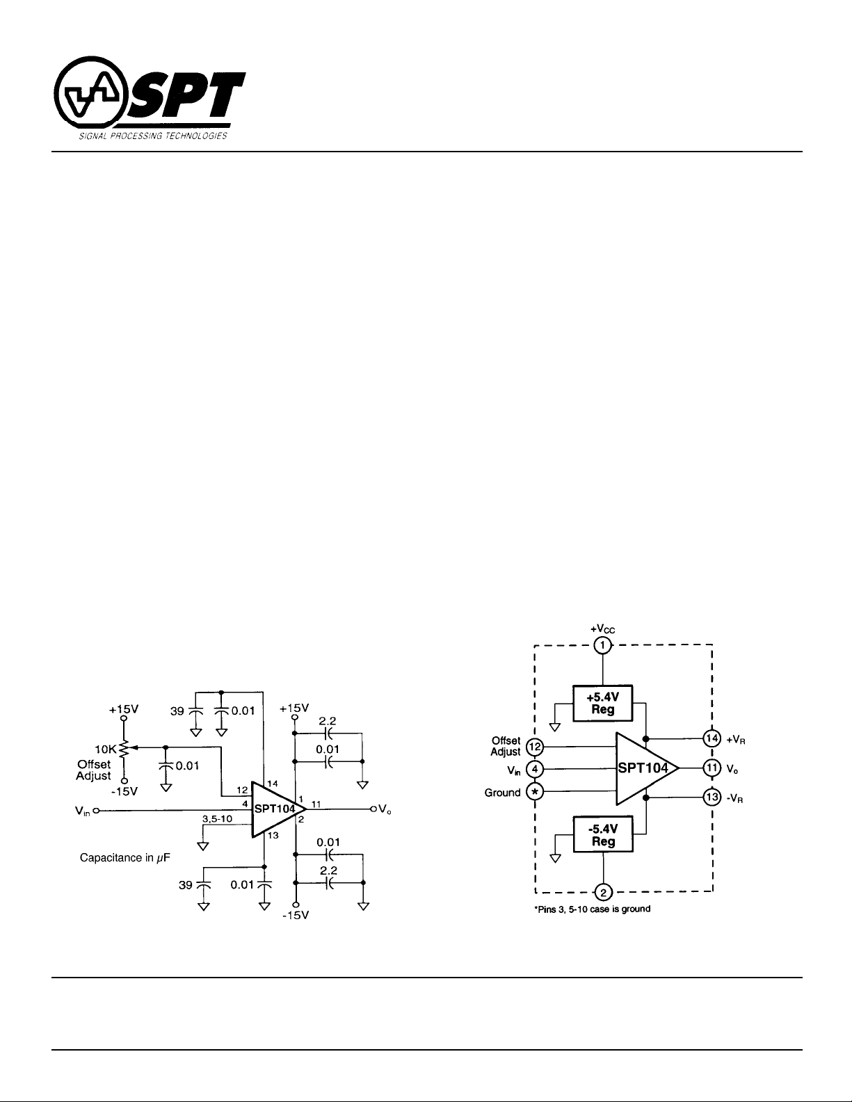
Basic Circuit Diagram
Equivalent Circuit Diagram
Signal Processing Technologies, Inc.
4755 Forge Road, Colorado Springs, Colorado 80907, USA
Phone: (719) 528-2300 FAX: (719) 528-2370 Website: http://www.spt.com E-Mail: sales@spt.com

SPT104 ELECTRICAL CHARACTERISTICS (T
PARAMETERS CONDITIONS TYP MIN & MAX RATINGS UNITS SYM
Ambient Temperature +25°C Min Max
FREQUENCY DOMAIN RESPONSE
† -3dB bandwidth 0dBm out 1100 1000 MHz SSBW
10dBm out 1050 MHz SSBW
† non-inverting gain (note 1) @ 100MHz 14.2 13.8 14.9 dB
† gain flatness DC - 750MHz ±0.4 -0.6 +0.6 dB
linear phase deviation DC - 600MHz 1.5 3 ° LPD
group delay 600 ps GD
reverse isolation
DC - 750MHz 40 dB RINI
750MHz - 1100MHz 35 dB RIIN
input return loss DC - 750MHz 18 dB
750MHz - 1100MHz 11 dB
output return loss DC - 750MHz 17 dB
750MHz - 1100MHz 10 dB
TIME DOMAIN RESPONSE
rise and fall time 1V step 325 375 ps TRS
(10% to 90%) 2V step 375 450 ps TRL
settling time to 0.8% 1V step 1.2 ns TS
overshoot 1V step 3 % OS
overload recovery V
NOISE AND DISTORTION RESPONSE
† 2nd harmonic distortion 0dBm, 100MHz 47 -dBc HD2
† 3rd harmonic distortion 0dBm, 100MHz 53 -dBc HD3
† 2nd harmonic distortion 10dBm, 100MHz 40 30 -dBc HD2
† 3rd harmonic distortion 10dBm, 100MHz 43 35 -dBc HD3
3rd order intermodulation intercept 100MHz 26 +dBm
2-tone, 1MHz separation 500MHz 17
equivalent input noise voltage 10Hz to 1200MHz 55 dB
noise figure 11 dB
usable dynamic range 100MHz 71 dB
= ±0.5V 1.2 1.6 ns OR
inpeak
500MHz 65 dB
= +25 °C, VCC = ±15V, RL = 50Ω, RS = 50Ω; unless specified)
A
STATIC, DC PERFORMANCE
input bias current note 2 80 280 µA IBN
input bias current (drift) note 2 0.6 2.0 µA/°C IBN
output offset voltage note 3 50 250 mV
output offset voltage (drift) note 3 375 625 µV/°C
* supply current no load 54 60 mA ICC
supply rejection ratio 1KHz 55 dB PSRR
Min/max ratings are based on product characterization and simulation. Individual parameters are tested as noted. Outgoing quality levels are
determined from tested parameters.
Absolute Maximum Ratings
V
CC
I
O
input voltage ±0.5V
junction temperature +175°C
operating temperature AI: -25°C to +85°C
storage temperature -65°C to +150°C
±9V to ±16V
±40mA
1. Nominal gain only - gain variation over temperature is ±0.1dB.
2. Input offset voltage = (input bias current) x (R
3. Output offset can be adjusted to zero with an external potentiometer – see “Reducing DC Offset”.
4. * AI 100% tested at 25°C.
† AI Sample tested at 25°C.
Notes
|| 50Ω).
S
SPT104
SPT
2 9/30/99
 Loading...