SPT HCMP9650SID, HCMP9650SCU Datasheet

FEATURES
• Propagation Delay of 2.4 ns (typ)
• Propagation Delay Skew <300 ps
• Low Offset ±3 mV
• Latch Control
GENERAL DESCRIPTION
The HCMP96850 is a single, very high speed monolithic
comparator. It is pin-compatible with and has improved
performance over the AD9685 and the AM6685. The
HCMP96850 is designed for use in Automatic Test Equipment (ATE), high speed instrumentation, and other high
speed comparator applications.
APPLICATIONS
• High Speed Instrumentation, ATE
• High Speed Timing
• Window Comparators
• Line Receivers
• A/D Conversion
• Threshold Detection
HCMP96850
SINGLE UL TRAFAST VOL T AGE COMPARA TOR
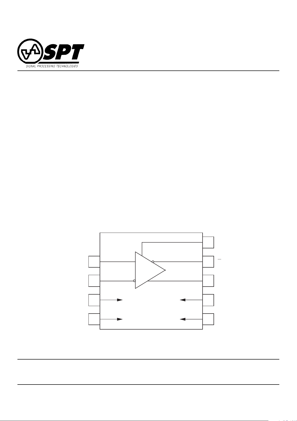
BLOCK DIAGRAM
-
+
NONINVERTING
INPUT
INVERTING
INPUT
GND
1
V
EE
GND
2
V
CC
LATCH ENABLE
Q OUTPUT
Q OUTPUT
Improvements over other sources include reduced power
consumption, reduced propagation delays, and higher input
impedance.
The HCMP96850 is available in a 16-lead ceramic DIP
package over the industrial temperature range. It is also
available in die form.
Signal Processing Technologies, Inc.
4755 Forge Road, Colorado Springs, Colorado 80907, USA
Phone: (719) 528-2300 FAX: (719) 528-2370 Website: http://www.spt.com E-Mail: sales@spt.com

SPT
2 3/18/97
HCMP96850
ELECTRICAL SPECIFICATIONS
T A = +25 °C, VCC = +5.0 V, VEE = -5.2 V, RL = 50 Ohms, unless otherwise specified.
TEST TEST
PARAMETERS CONDITIONS LEVEL MIN TYP MAX UNITS
DC ELECTRICAL CHARACTERISTICS
Input Offset Voltage RS = 0 Ohms
1
IV -3 +3 mV
Input Offset Voltage (Vos)R
S
= 0 Ohms,
1
T
MIN
<TA<T
MAX
IV -3.5 +3.5 mV
(Vos) Tempco V 4 µV/°C
Input Bias Current I 4 ±20 µA
Input Bias Current T
MIN
<TA<T
MAX
IV 7 µA
Input Offset Current I -1.0 +1.0 µA
Input Offset Current T
MIN
<TA<T
MAX
IV -1.5 +1.5 µA
Positive Supply Current I 3.3 5 mA
Negative Supply Current I 13.5 18 mA
Positive Supply Voltage, V
CC
IV +4.75 +5.0 +5.25 V
Negative Supply Voltage, V
EE
IV -4.95 -5.2 -5.45 V
Input Common Mode Range I -2.5 +2.5 V
Latch Enable
Common Mode Range IV -2 0 V
Open Loop Gain V 4000 V/V
Input Resistance V 60 kΩ
Input Capacitance V 3 pF
Input Capacitance (LCC Package) V 1 pF
Power Supply Sensitivity VCC and V
EE
V70dB
Common Mode Rejection Ratio V 80 dB
Power Dissipation I
OUTPUT
= 0 mA IV 90 120 mW
ABSOLUTE MAXIMUM RATINGS (Beyond which damage may occur)1 25 °C
Supply Voltages
Positive Supply Voltage (VCC to GND) .... -0.5 to +6.0 V
Negative Supply Voltage (VEE to GND) ... -6.0 to +0.5 V
Ground Voltage Differential ...................... -0.5 to +0.5 V
Input Voltages
Input Voltage ............................................ -4.0 to +4.0 V
Differential Input Voltage .......................... -5.0 to +5.0 V
Input Voltage, Latch Controls ..................... VEE to 0.5 V
Output
Output Current......................................................30 mA
Temperature
Operating Temperature, ambient .............-25 to +85 °C
junction ...................... +150 °C
Lead Temperature, (soldering 60 seconds) ...... +300 °C
Storage Temperature ..............................-65 to +150 °C
Note: 1. Operation at any Absolute Maximum Rating is not implied. See Electrical Specifications for proper nominal
applied conditions in typical applications.

SPT
3 3/18/97
HCMP96850
ELECTRICAL SPECIFICATIONS
T A = +25 °C, VCC = +5.0 V, VEE = -5.2 V, RL = 50 Ohms, unless otherwise specified.
TEST TEST
PARAMETERS CONDITIONS LEVEL MIN TYP MAX UNITS
OUTPUT LOGIC LEVELS (ECL 10 KH Compatible)
Output High 50 Ohms to -2 V I -.98 -.81 V
Output Low 50 Ohms to -2 V I -1.95 -1.63 V
AC ELECTRICAL CHARACTERISTICS
2
Propagation Delay 10 mV O.D. III 2.4 3.0 ns
Latch Set-up Time IV 0.6 1 ns
Latch to Output Delay 50 mV O.D. IV 3 ns
Latch Pulse Width V 2 ns
Latch Hold Time IV 0.5 ns
Rise Time 20% to 80% V 1.76 ns
Fall Time 20% to 80% V 1.76 ns
1
RS = source impedance.
2
100 mV input step.
TEST LEVEL CODES
All electrical characteristics are subject to the
following conditions:
All parameters having min/max specifications
are guaranteed. The Test Level column indicates the specific device testing actually performed during production and Quality Assurance inspection. Any blank section in the data
column indicates that the specification is not
tested at the specified condition.
TEST PROCEDURE
100% production tested at the specified temperature.
100% production tested at TA=25 °C, and sample
tested at the specified temperatures.
QA sample tested only at the specified temperatures.
Parameter is guaranteed (but not tested) by design
and characterization data.
Parameter is a typical value for information purposes
only.
100% production tested at TA = 25 °C. Parameter is
guaranteed over specified temperature range.
TEST LEVEL
I
II
III
IV
V
VI
 Loading...