

Page 1
APPROVAL SHEET
Power supply
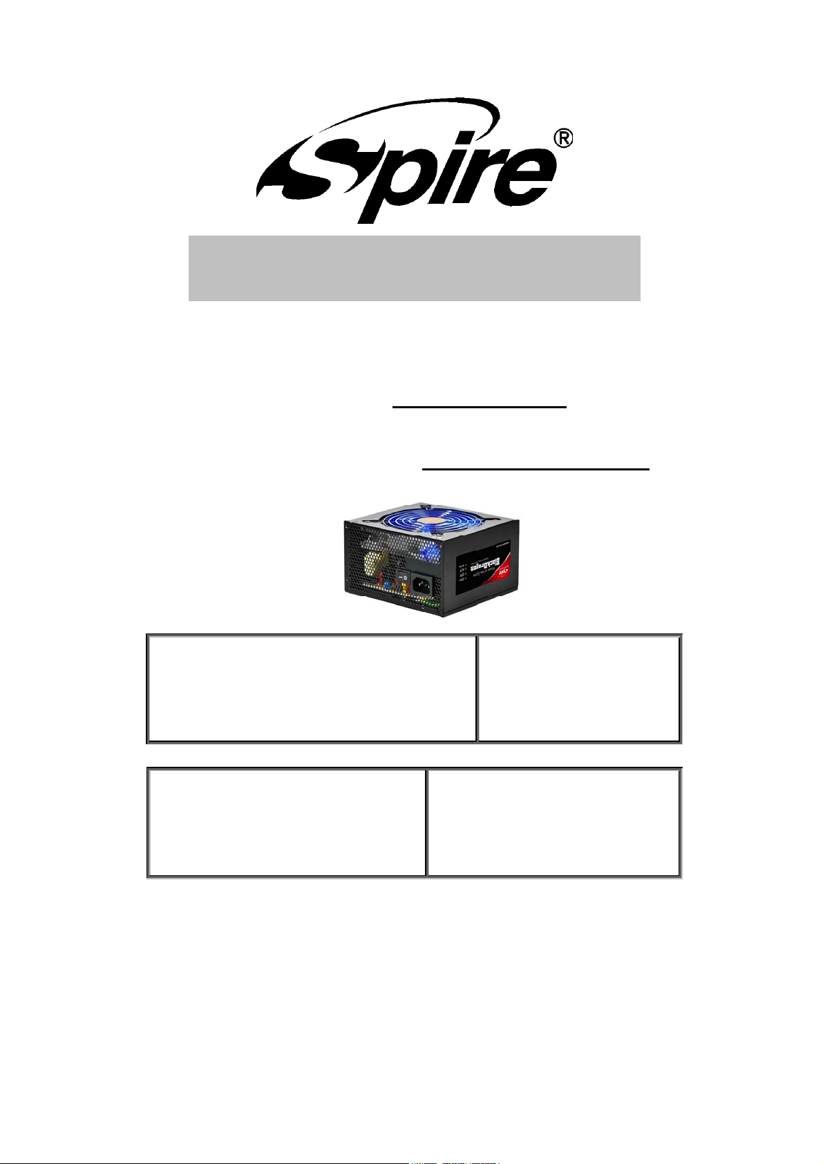
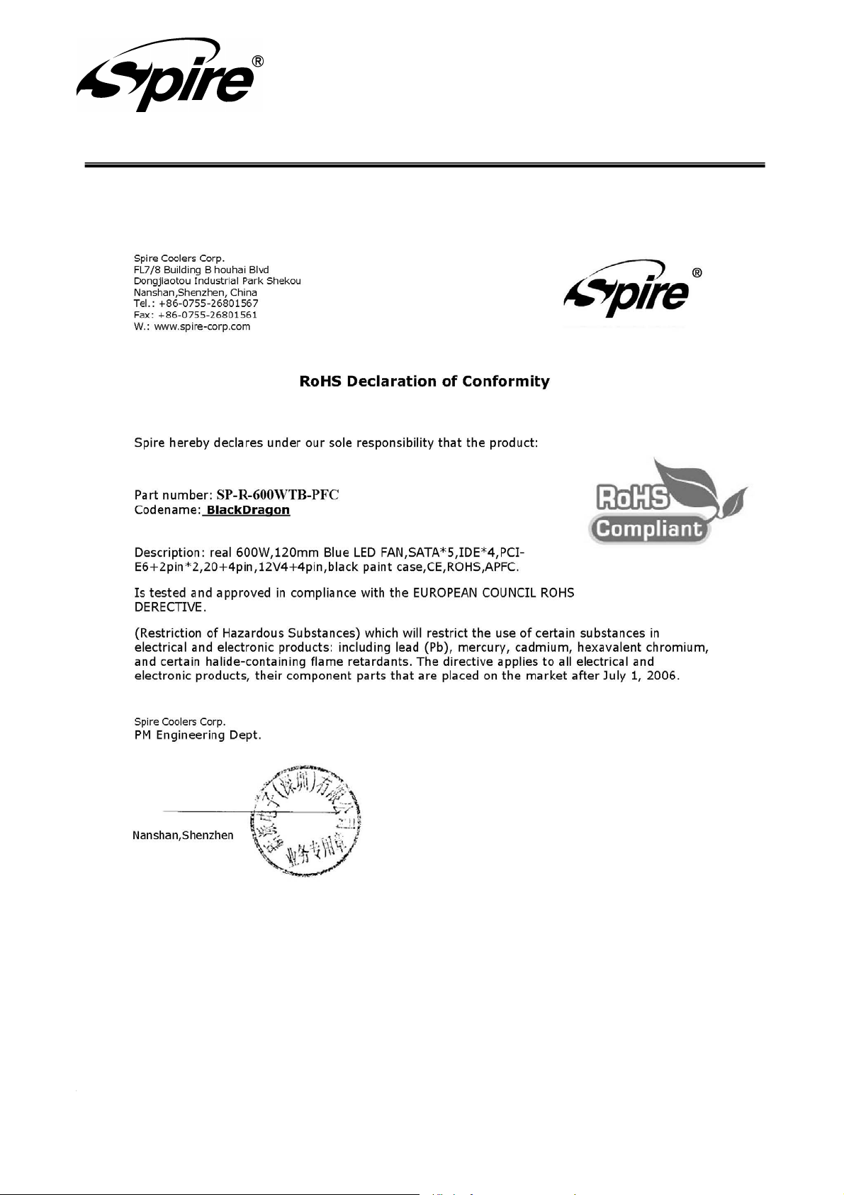
MODEL NO: SP-R-600WTB-PFC
ENGINEER NO: SUATX0600Z1ECAEU111
Article No. : SP-AP-SU-A128
Issue Date :2010-10-24
Version : A/0
Audited by
Checked by
Drafted by
Spire Corp.
Tel.: +86-755-26801567 Fax: +86-755-26801561
Version:A/0
Http://www.spire-corp.com
Http://www.spirepower.com
Http://www.spirecoolers.com
Page 2
Spire Corp.
Approval Sheet Revisement Record
Article No: SP-AP-SU-A128
Version
Description
Chapter
A/0 N/A First Version N/A
Revised
Revised
Date
Drafted
by
Audited
by
ECN
No.
Version:A/0 Page 2 of 18
Http://www.spirepower.com & Http://www.spirecoolers.com
Http://www.spire-corp.com
Page 3

Spire Corp.
Contents
1 Introduction………………………………………………………………5
1.1 Scope………………………………………………………………………5
1.2 General Description………………………………………………….……5
2 Electrical………………………………………………………………………5
2.1 AC Input…………………………………………………..………………5
2.1.1 Input Over current Protection……………………………………5
2.1.2 Inrush Current Limiting…………………………….………………6
2.1.3 Withstand Voltage……………………………......……………...6
2.1.4 Catastrophic Failure Protection……………………….…………..6
2.2 DC Output……………………………………………………….…………6
2.2.1 DC Voltage Regulation……………….……………………………6
2.2.2 Output DC Current Ranges……….………………………………7
2.2.3 Output Voltage Line Regulation. ………………..………….….…7
2.2.4 Cross Regulation…………………………………..……………….7
2.2.5 Efficiency ………………………………………………..................8
2.2.6 Output Ripple/Noise………………………………………………..8
2.2.7 Output Transient Response…………...…………………………..9
2.2.8 Capacitive Load …………………………………………………….9
2.2.9 Closed-loop Stability ……………………………………………….9
2.2.10 Power Sequencing………………………………………………...9
2.2.11 Voltage Hold-up Time…………………………………..………10
2.3 Timing / Housekeeping / Control…………………….…………………..10
2.3.1 PWR_OK……………………………………….…………………10
2.3.2 PS_ON#…………………………………………………..………11
2.3.3 +5VSB……………………..……………….……………….……11
2.3.4 Power-on Time…………………………………...………………11
2.3.5 Rise time………………………………………………………..…11
2.3.6 Overshoot at Turn-on /Turn-off…………………………..………11
2.3.7 Reset after Shutdown…………………………………………… …11
Version:A/0 Page 3 of 18
Http://www.spirepower.com & Http://www.spirecoolers.com
Http://www.spire-corp.com
Page 4

Spire Corp.
2.4 Output Protection…………………………………………………………12
2.4.1 Over voltage Protection…………………………………………12
2.4.2 Over Current Protection…………………………………………12
2.4.3 Short-circuit Protection……………………………………………12
3 Mechanical……………………………………………………..……………12
3.1 AC Connector. ………………………………..…………………………12
3.2 DC Connector Pin Description…………………….……..……………13
4 Environmental…………………………..……………………………………14
4.1 Environmental (Operating)…………………..…………………………14
4.2 Environmental (Non-Operating)…………..……………………………14
5 Electromagnetic Compatibility…………………………..…………………14
5.1 EMI…………………………………………………..……………………14
6 Reliability……………………………………………………………………15
6.1 Component Derating………………………………………..……………..15
6.2 Mean Time Between Failures(MTBF)…………………..……………15
7 Connectors& cables diagram ……………………………………………16
8 Photograph …………………………………………………..…………………17
Version:A/0 Page 4 of 18
Http://www.spirepower.com & Http://www.spirecoolers.com
Http://www.spire-corp.com
Page 5
1 Introduction
1.1 Scope
This specification defines the performance and characteristic for the model of
SP-R-600WTB-PFC power supply.
1.2 General Description
SP-R-600WTB-PFC is a switching power supply, 600W self-contained, AC to DC
power source supply suitable for mounting in PC.
1) SPCC 0.8MM ENCLOSURE
2) one 120mm transparency with blue LED fan
3) Black Paint Case
4) Dimensions:140mm(L)X150mm(W)X85mm(H)
2 Electrical
2.1 AC Input
Spire Corp.
Table 1 list AC input voltage and frequency requirements for continuous operation.
Parameter Min. Nom.
Vin Voltage 90 110--230 253
Vin Frequency 50 --- 60 Hzrms
(1)
Nominal voltages for test purposes are considered to be within ±1.0 V of nominal.
Table 1. AC Input Line Requirements
(1)
Max. Unit
VACrm s
Power Factor Correction (PFC)
SP-R-600WTB-PFC (w/ Active PFC) is facilitated with the universal input
110~240VAC Active PFC with the PF value ≧ 0.9
2.1.1 Input Over Current Protection
The power supply is equipped with a non-reset-able fuse on the AC
input to limit power consumption on a failure within the power supply
module.
Input Fuse Rating:
Voltage 250 V
Current 10A
De-activation time 200 ms
Version:A/0 Page 5 of 18
Http://www.spirepower.com & Http://www.spirecoolers.com
Http://www.spire-corp.com
Page 6
Spire Corp.
2.1.2 Inrush Current Limiting
Maximum inrush current from power-on (with power on at any point on the AC
sine) and including, but not limited to, three line cycles, shall be limited to a
level below the surge rating of the input line cord, AC switch if present, bridge
rectifier, fuse, and EMI filter components. Repetitive ON/OFF cycling of the AC
input voltage should not damage the power supply or cause the input fuse to
blow.
2.1.3 Withstand Voltage
The power supply is capable of withstanding a maximum 1500 VDC
potential between the input and ground for a period of 1 second.
2.1.4 Catastrophic Failure Protection
If a component failure occurs, the power supply will not exhibit any of
the following:
1) Flame
2) Excessive smoke
3) Charred PCB
4) Fused PCB conductor
5) Startling noise
6) Emission of molten material
2.2 DC Output
2.2.1 DC Voltage Regulation
The DC output voltages are remain within the regulation ranges shown in Table
2 when measured at the load end of the output connectors under all line, Load,
and environmental conditions.
Table 2. DC Input Line Requirements
Output Range Min. Nom.(1) Max. Unit
+12V1DC ± 5% +11.40 +12.00 +12.60
+12V2DC ± 5% +11.40 +12.00 +12.60
+12V3DC ± 5% +11.40 +12.00 +12.60
+5VDC ± 5% +4.75 +5.00 +5.25
Volts
Volts
Volts
Volts
+3.3VDC ± 5% +3.14 +3.30 +3.47 Volts
-12VDC ± 10% -10.80 -12.00 -13.20
+5VSB ± 5% +4.75 +5.00 +5.25
1) ATX +12VDC peak loading, regulation at the + 12Vdc output can go to±10%.
Version:A/0 Page 6 of 18
Http://www.spirepower.com & Http://www.spirecoolers.com
Http://www.spire-corp.com
Volts
Volts
Page 7
Spire Corp.
2.2.2 Output DC Current Ranges
All outputs are within the specified limits of regulation when each output is
subjected to the conditions listed below.
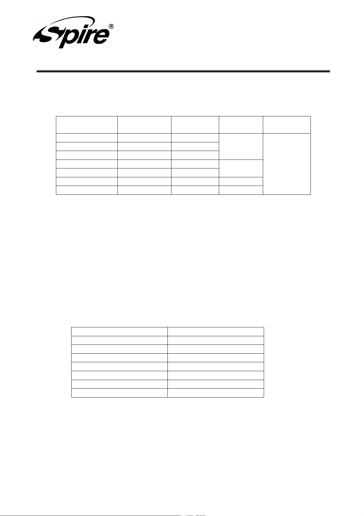
Table 3. DC Input Line Requirements
DC Nominal
Voltage
Minimum
Current
+12 V1 DC 1.0 A 20A
+12 V2 DC 1.0 A 20A
+12 V3 DC 1.0 A 20A
+5 V DC 0.2 A 20A
Maximum
Current
Combined Output
574W
160W
600W
+3.3 V DC 0.1 A 20A
- 12 V DC 0.0 A 0.3A 3.6W
+5 V SB 0.05A 2.5A 12.5W
NOTE:
1)The combined power output of +5V and +3.3V shall not exceed 160W.
The combined power output of +5V,+3.3V and +12V shall not exceed 574W
3)Input voltage is 110-240Vac ,When peak load.
2.2.3 Output Voltage Line Regulation
The following table specifies line regulation as measured from
minimum to maximum load including the transient response
requirements as detailed in this document.
Table 4. DC Output Tolerance Specifications
DC Nominal Output Output Voltage Tolerance
+12V1 DC ±1%
+12V 2DC ±1%
+12V 3DC ±1%
+5V DC ±1%
+3.3V DC ±1%
-12V DC ±2%
+5V SB ±1%
2.2.4 Cross Regulation
The power supply DC outputs perform within all line and load specifications
Regardless of the static or transient loads on any of the outputs.
Version:A/0 Page 7 of 18
Http://www.spirepower.com & Http://www.spirecoolers.com
Http://www.spire-corp.com
Page 8
Spire Corp.
2.2.5 Efficiency
The minimum efficiency of power supply should be over than 82% under the
maximum and 20% load. And should be over 85% under the 50% load. Load
measurements are performed at 115VAC/230Vac input.
2.2.6 Output Ripple/Noise
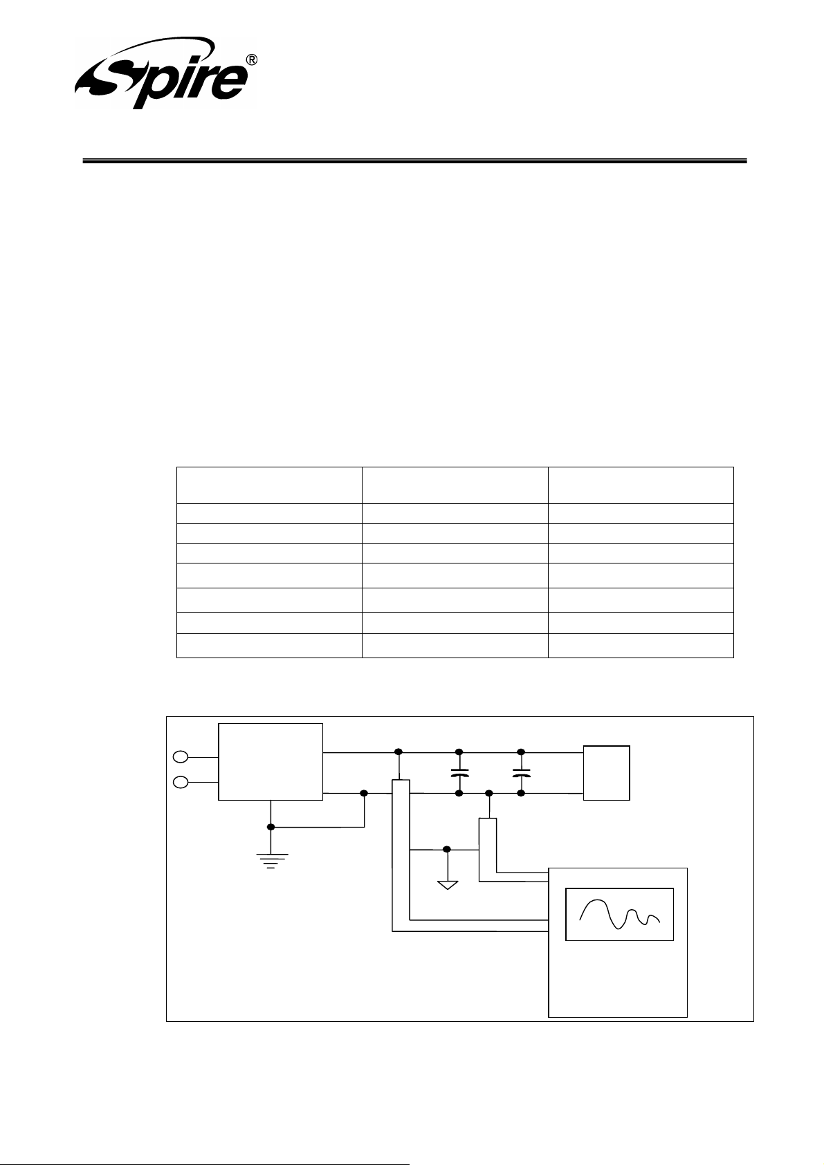
The output ripple/noise requirements listed in Table 5 should be met
throughout the load ranges specified and under all input voltage conditions as
specified. Ripple and noise are defined as periodic or random signals over a
frequency band of 10 Hz to 20MHz. Measurements shall be made with an
oscilloscope with 20 MHZ bandwidth. Outputs should be bypassed at the
connector with a 0.1μF ceramic disk capacitor and a 10μF electrolytic capacitor
to simulate system loading. See Figure1.
Output Max.Ripple& Noise Units
+12 V1DC 120 mV
+12 V2DC 120 mV
+12 V3DC 120 mV
+5 VDC 50 mV
+3.3 VDC 50 mV
-12 VDC 120 mV
+5 VSB 50 mV
Table 5. DC Output Ripple/Noise
Figure1. Differential Noise Test Setup
1.Load the output with its minimum load current.
2.Connect the probes as shown.
3.Repeat the measurement with maximum load on the output.
Version:A/0 Page 8 of 18
Power Supply
AC Hot
AC Neutral
Gene ral Notes:
AC Ground
V out
10
μ F
V return
Http://www.spirepower.com & Http://www.spirecoolers.com
Http://www.spire-corp.com
0.1
Loa d must be
ed from the
isolat
ground of the
power supply
Load
F
μ
Scope
Page 9
Spire Corp.
2.2.7 Output Transient Response
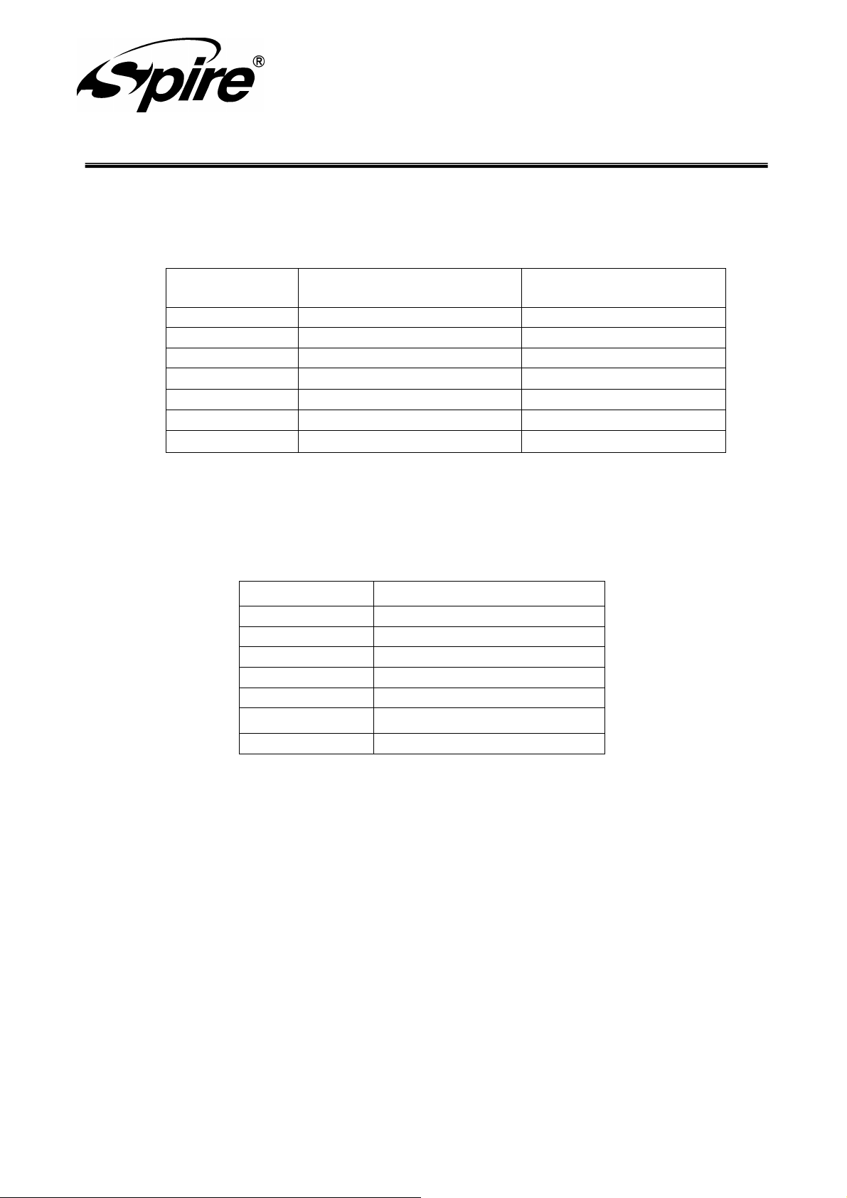
The table below summarizes the output transient steps for each output. The
Transient slew rate is =0.5A/μs.
Table 6. DC Output Transient Response Specifications
DC Output Maximum Step Size Output Voltage Tolerance
+12V1DC 40% of rated output ±5%
+12V2DC 60% of rated output ±5%
+12V3DC 60% of rated output ±5%
+5VDC 30% of rated output ±5%
+3.3VDC 30% of rated output ±5%
-12VDC 0.1A ±10%
+5VSB 0.5A ±5%
2.2.8 Capacitive Load
The power supply is able to power up and operate normally with the following
capacitances simultaneously present on the DC outputs.
Table 7. Output Capacitive Loads
DC Output ATX12V Capacitive Load (μF)
+12 V1DC 10,000
+12 V2DC 10,000
+12 V3DC 10,000
+5 VDC 10,000
+3.3 VDC 10,000
-12 VDC 350
+5 VSB 2000
2.2.9 Closed-loop Stability
The power supply is unconditionally stable under all line/load/transient loads
Conditions including capacitive loads specified in Table 7. A minimum of 45
degrees phase margin and 10 dB gain margin is recommended at both the
maximum and minimum loads.
2.2.10 Power Sequencing
All outputs, regardless of loading, turn on within 50ms of each other. The 5VSB
output is in regulation for a minimum of 10ms prior to the other output rails
reaching regulation.
Version:A/0 Page 9 of 18
Http://www.spirepower.com & Http://www.spirecoolers.com
Http://www.spire-corp.com
Page 10
2.2.11 Voltage Hold-up Time
All output will stay within regulation for at least 16ms after an AC line voltage
failure is detected at nominal line (230VAC) under full load condition.
2.3 Timing / Housekeeping / Control
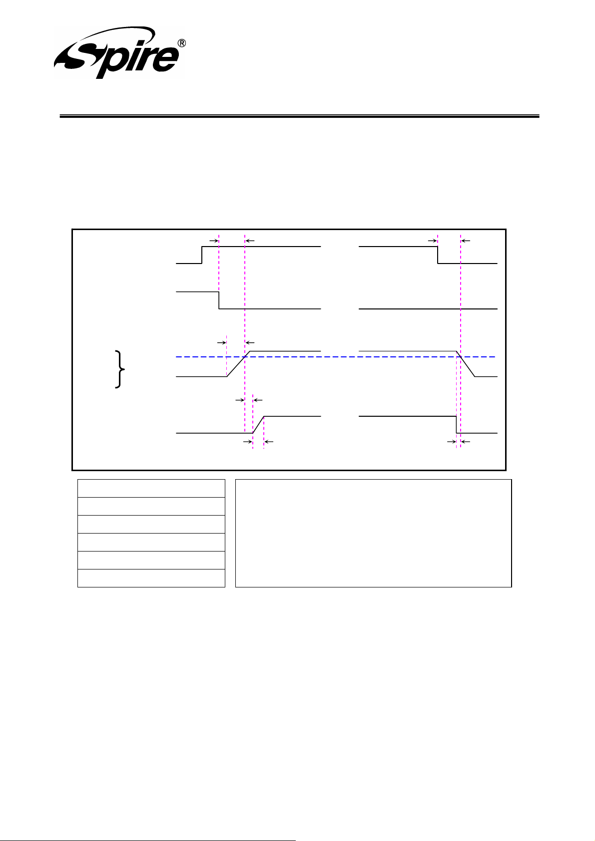
Figure 2. Power Supply Timing
VAC_ON
VAC_OFF
PS_OFF#
PS_ON#
T1
+12VDC
+5VDC O/P’s
+3.3VDC
95%
10%
T2
T3
PWR_OK Sense Level=95% of nominal
PWR_OK
T4
~
~
~
~
Spire Corp.
T5
T6
T1 < 100ms
0.2ms ≦ T2 ≦ 20ms
100ms < T3 < 500ms
T4 ≦ 10ms
T5 ≧ 16ms
T6 ≧ 1ms
T1:Power-on Time
T2:Rise Time
T3:PWR_OK Delay
T4:PWR_OK Risetime
T5:AC Loss to PWR_OK Hold-up Time
T6:Power-down Warning
2.3.1 PWR_OK
The power supply accepts a logic collector level which will disable/enable
all the output voltages. As the logic level is low, output voltages are enable;
As the logic level is high, output voltages are disable. The definition of
logic low/high level is as:
High Level: 2.50V ~ 5.25V while sourcing 0.4mA maximum
Low Level: 0.0V ~ 0.50V while sinking 5.0mA maximum
Rise Time: 3.0ms maximum (10.0% ~ 90.0%)
Version:A/0 Page 10 of 18
Http://www.spirepower.com & Http://www.spirecoolers.com
Http://www.spire-corp.com
Page 11
Spire Corp.
2.3.2 PS_ON#
The power supply provides an internal pull-up to TTL high. The power supply
also provides denounce circuitry on PS_ON# to prevent it from oscillating
on/off at startup when activated by a mechanical switch. The DC output enable
circuitry is SELV-complaint.
VIL, Input Low Voltage 0.0V 0.8V
VIL, Input Low Current (Vin = 0.4 V) -1.6mA
VIH, Input High Voltage (lin = -200 μA) 2.0V
VIH, open circuit, lin = 0 5.25V
Table 8. PS_ON# Signal Characteristics
Min. Max.
2.3.3 +5VSB
The +5VSB is capable of delivering a maximum of 2.5A at +5V ±5% to external
circuit. The power supply +5VSB is with overcurrent protection.
2.3.4 Power-on Time
The power-on time is less than 100ms (T1 < 100ms). The +5VSB has a
power-on time of two seconds maximum after application of valid AC
voltages. (Figure 1)
2.3.5 Rise time
The output voltages rise from ≤ 10% of nominal to within the regulation ranges
within 0.2ms to 25ms ( 0.2ms ≤ T2 ≤ 25ms). (Figure 2)
2.3.6 Overshoot at Turn-on / Turn-off
Any overshoot at turn on or turn off is under 10% of the nominal DC
output voltage with further stipulation that all DC outputs are within their
specified DC voltage ranges before the generation of the power good
signal. Additionally, no voltage may undershoot or overshoot once the
power good signal has been asserted.
2.3.7 Reset after Shutdown
The power supply latches into a shutdown state because of a fault condition
on its outputs, the power supply returns to normal operating after the fault
has been removed and the PS_ON# (or AC input) has been cycled OFF/ON
with a minimum OFF time of 1 second.
Version:A/0 Page 11 of 18
Http://www.spirepower.com & Http://www.spirecoolers.com
Http://www.spire-corp.com
Page 12

2.4 Output Protection
Each DC output is protected from over voltage, over current and short circuit. The
following sections include the details for these protection mechanisms.
2.4.1 Over voltage Protection
The overvoltage sense circuitry and reference reside in packages that are
separate and distinct from the regulator control circuitry and reference. No
single point fault is able to cause a sustained overvoltage condition on any
or all outputs. The power supply provides latch-mode overvoltage
protection defined as:
+5V output is between 5.74V to 7V
+12V output is between 13.4V to 15.6V
+3.3V output is between 3.76V to 4.8V
2.4.2 Over Current Protection
Spire Corp.
The power supply should provide +5V, +3.3Vand +12V OCP and should
shutdown of each output power. For testing purposes, the overload currents of
each tested output rail should be ramped at a minimum rate of 10A/sec.
2.4.3 Short-circuit Protection
The short circuit placed on +3.3V, +5V, + 12V, –12V and 5Vs output shall
cause no damage and the power supply shall shut down or latch.
3 Mechanical
3.1 AC Connector
The AC input receptacle is an IEC 320 type or equivalent. In lieu of a dedicated
switch, the IEC 320 receptacle may be considered the mains disconnect.
Version:A/0 Page 12 of 18
Http://www.spirepower.com & Http://www.spirecoolers.com
Http://www.spire-corp.com
Page 13
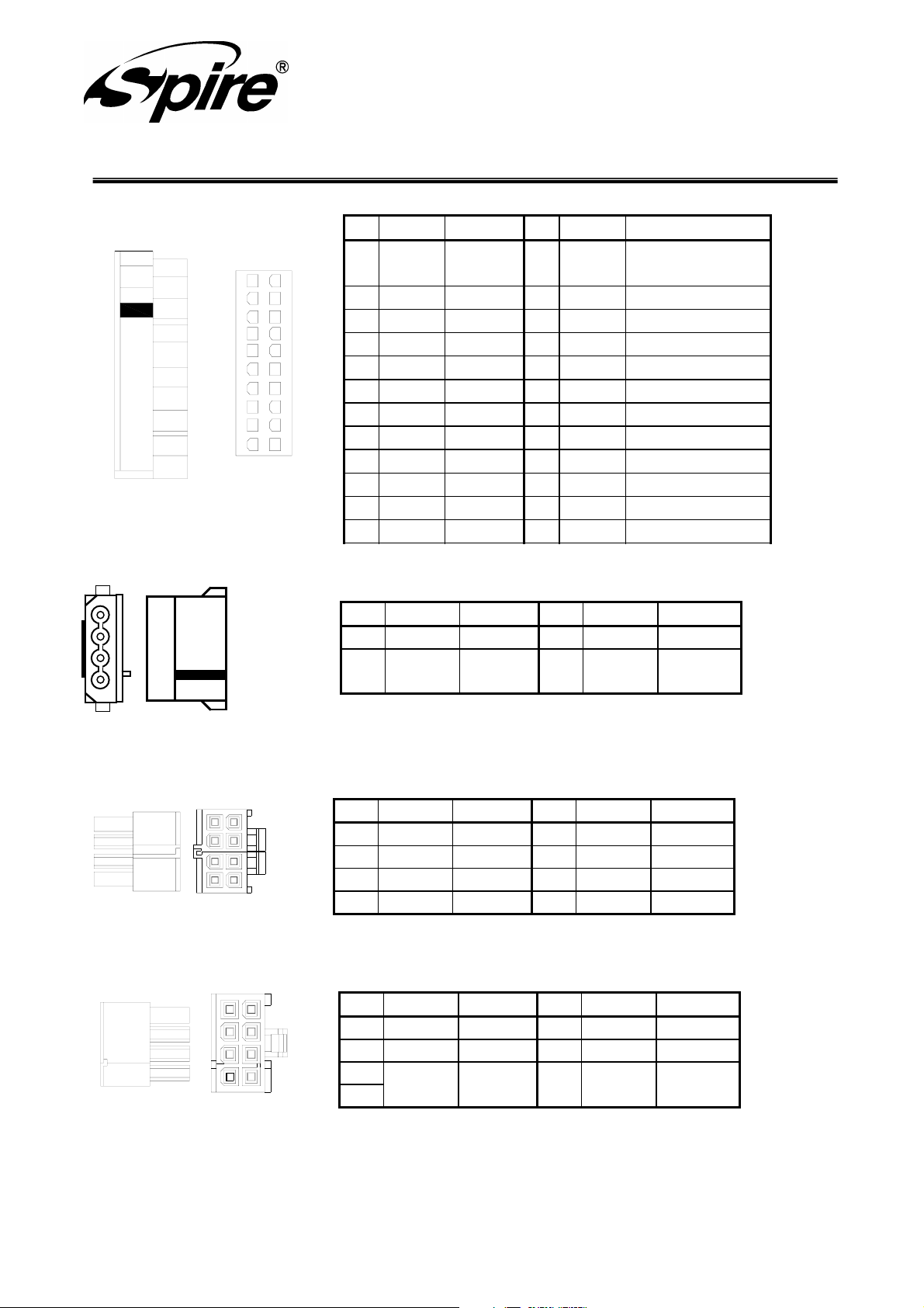
3.2 DC Connector Pin Description
IN1 PIN13
Spire Corp.
Pin Color Signal Pin Color Signal
1 Orange +3.3VDC 13
2 Orange +3.3VDC 14 Blue -12VDC
3 Black COM 15 Black COM
4 Red +5VDC 16 Green PS_ON/OFF
5 Black COM 17 Black COM
6 Red +5VDC 18 Black COM
7 Black COM 19 Black COM
8 Gray PWR_OK 20
9 Purple +5VSB 21 Red +5VDC
10 Yellow +12VDC 22 Red +5VDC
11 Yellow +12VDC 23 Red +5VDC
12 Orange +3.3VDC 24 Black COM
Orange
Brown
+3.3VDC
+3.3V default sense
1
2
3
4
Pin Color Signal Pin Color Signal
1
1 Red +5VDC 3 Black COM
2
3
2 Black COM 4 Yellow
4
5
6
7
8
Pin Color Signal Pin Color Signal
1 Black COM 5 Yellow +12VDC
2 Black COM 6 Yellow +12VDC
3 Black COM 7 Yellow +12VDC
4 Black COM 8 Yellow +12VDC
Pin Color Signal Pin Color Signal
1 Yellow +12VDC 5 Black COM
2 Yellow +12VDC 6 Black COM
3 Yellow +12VDC 7 Black COM
4 Black COM 8 Black COM
+12VDC
Version:A/0 Page 13 of 18
Http://www.spirepower.com & Http://www.spirecoolers.com
Http://www.spire-corp.com
Page 14

Spire Corp.
4 Environmental
4.1 Environmental (Operating)
Temperature: 0℃ to 50℃
Humidity: 5% to 90% Relative Humidity (non condensing)
Altitude: 0 meters to +3,048 meters
Shock: T.B.S.
Vibration: T.B.S.
4.2 Environmental (Non-Operating)
Temperature: -40 to ℃ 70℃
Humidity: 5% to 85% Relative Humidity (non condensing)
Altitude: 0 meters to +15,244 meters
Shock: T.B.S.
Vibration: T.B.S.
5 Electromagnetic Compatibility
The following subsections outline sample product regulations requirements for a typical
Power supply. Actual requirements will depend on the design, product end use, target
Geography, and other variables. Consult your company’s Product Safety and Regulations
Department for more details
5.1 EMI
The power supply shall comply with CISPR 22, Class B. Tests shall be conducted using a
shielded DC output cable to a shielded load. The load shall be adjusted as follows
condition: Test with system; Tests will be performed at 115VAC/60Hz, and 220VAC/50Hz.
Version:A/0 Page 14 of 18
Http://www.spirepower.com & Http://www.spirecoolers.com
Http://www.spire-corp.com
Page 15

6 Reliability
6.1 Component Derating
The following component derating guedelines are recommended:
‧Semiconductor junction temperatrues shall not exceed 110℃ with an ambient
of 50℃.
‧Inductor case temperature shall not exceed safety agency requirements.
‧Capacitor case temperature shall not exceed 95% of rated temperature.
‧Component voltage and current derating shall be >10% at 50℃.
‧Magnetic saturation of any transformer will not be allowed under any line, load,
startup or transient condition including 100% transients on the five main outputs or
+5VSB.
6.2 Mean Time Between Failures(MTBF)
The power supply reliability is based on the calculation with the Part-Stress Analysis
method of MIL-HDBK-217F using the quality factors listed in
MIL-HDBK-217F. The power supply MTBF is 100,000 hours under the
following conditions:
Spire Corp.
- Full-rated load
- 230VAC input
- Ground begin
- 25℃ ambient
Version:A/0 Page 15 of 18
Http://www.spirepower.com & Http://www.spirecoolers.com
Http://www.spire-corp.com
Page 16
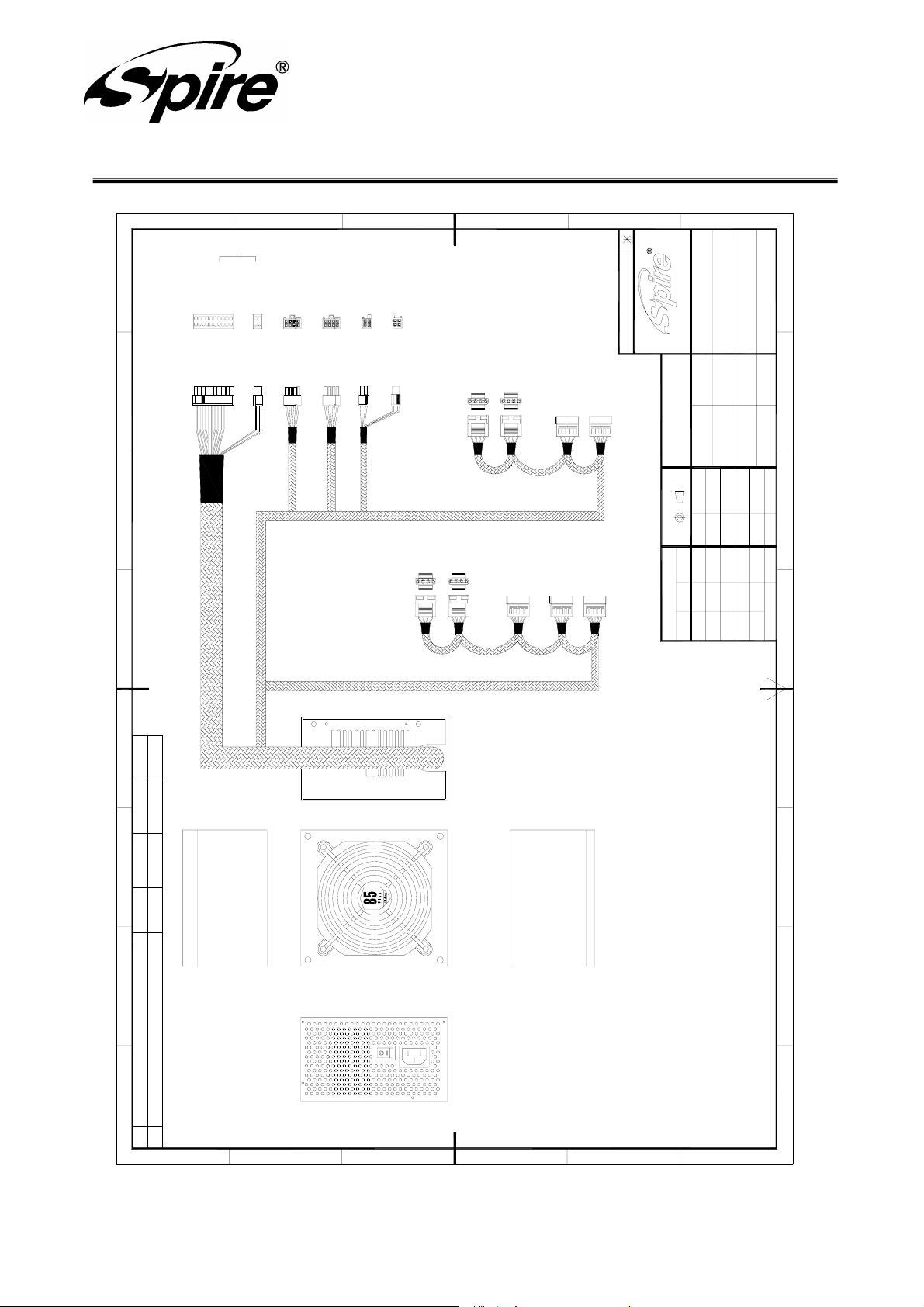
7 Connectors and cables diagram :
A
20+4
B
C
(GND)BLACK
(GND)BLACK
(GND)BLACK
(GND)BLACK
(GND)BLACK
(11)3.3V ORANGE/BROWN
(12)-12V BLUE
(13)COM BLACK
(14)PS-ON/OFF GREEN
(15)COM BLACK
(16)COM BLACK
(17)COM BLACK
(18)-5V WHITE
(19)5V R ED
PIN1 PIN13
(20)5V R ED
PIN1 PIN3
(03)5V RED
(04)COM BLACK
(GND)BLACK
PIN1 PIN4
(GND)BLACK
(GND)BLACK
PIN1 PIN4
(12V2DC) YELLOW
(12V2DC) YELLOW
PIN1 PIN3
(12V2DC) YELLOW
(12V2DC) YELLOW
PIN1 PIN3
(01)3.3V ORANGE
(02)3.3V ORANGE
(03)COM BLACK
(04)5V RE D
(05)COM BLACK
(06)5V RE D
(07)COM BLACK
(08)PWR-OK GRAY
(09)5VSB PURPLE
(10)12V YELLOW
(01)12V YELLOW
(02)3.3V ORANGE
(12VDC)YELLOW
(12VDC)YELLOW
(12VDC)YELLOW
(12VDC)YELLOW
(12VDC)YELLOW
(12VDC)YELLOW
(GND)BLACK
(GND)BLACK
(GND)BLACK
(GND)BLACK
(GND)BLACK
(GND)BLACK
(+5V)RED
(+5V)RED
(GND)BLACK
(GND)BLACK
(+12V)YELL OW
(+5V)RED
(GND)BLACK
DATE
Approved
Checked
Drawn
2
DESCRIPTION
1345678
REV
A
B
C
Spire Corp.
D
(GND)BLACK
(GND)BLACK
(+12V)YELLOW
(+5V)RED
(GND)BLACK
(GND)BLACK
(+12V)YELLOW
(+3.3V)ORANGE
(GND)BLACK
(+5V)RED
(GND)BLACK
(+12V)YELLOW
SATA SATA
(GND)BLACK
(+12V)YELL OW
(+3.3V)ORANGE
(GND)BLACK
(+5V)RED
(GND)BLACK
(+12V)YELL OW
(+12V)YELL OW
SATA SATA
(+3.3V)ORANGE
(GND)BLACK
(+5V)RED
SATA
(GND)BLACK
D
(+3.3V)ORANGE
(GND)BLACK
(+3.3V)ORANGE
(GND)BLACK
(+5V)RED
(GND)BLACK
(+5V)RED
(GND)BLACK
(+12V)YELL OW
E
Inspection Items
(+12V)YELLOW
Spire Corp.
SP-R-600WTB-PFC
File Name
THIRD ANGLE PROJECTION
TOLERANCE
TO
UNSPECIFIED TOLLERENCE
OVER
E
Part No.
Date
APVD
±0.10
10
0
mm
Unit
F
SP-BOM-SU-A137
SP-AP-SU-A128
SP-DR-SU-A136
SP-R-600WTB-PFC
Article No.
BOM No.
Spec No.
Date
Date
CHK. BY
DSN. BY Date
DRN. BY
A/0
1/1
N/A
N/A
- -
Version
Material
±0.30
100
30
Finish
±0.40
250
100
±0.50
over
250
Page
±0.5 °
Angles
Scale
±0.20
30
10
21345678
F
Version:A/0 Page 16 of 18
Http://www.spirepower.com & Http://www.spirecoolers.com
Http://www.spire-corp.com
Page 17
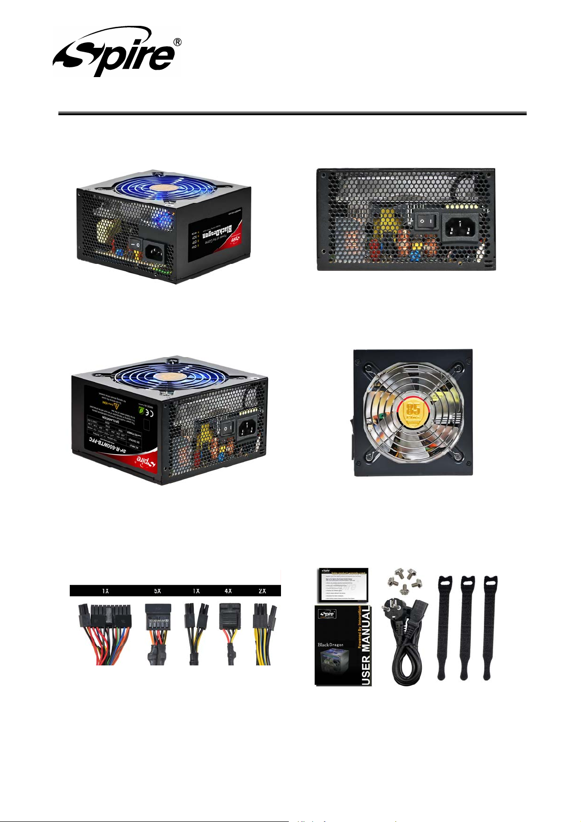
8 Photograph:
Spire Corp.
Version:A/0 Page 17 of 18
Http://www.spirepower.com & Http://www.spirecoolers.com
Http://www.spire-corp.com
Page 18
Spire Corp.
Version:A/0 Page 18 of 18
Http://www.spirepower.com & Http://www.spirecoolers.com
Http://www.spire-corp.com
 Loading...