

Page 1
PulseBlasterDDS™
Model DDS-III
(PCI Board SP3)
Owner’s Manual
SpinCore Technologies, Inc.
http://www.spincore.com
Page 2

PulseBlasterDDS
Congratulations and thank you for choosing a design from
SpinCore Technologies, Inc.
We appreciate your business!
At SpinCore we try to fully support the needs of our customers. If you
are in need of assistance, please contact us and we will strive to
provide the necessary support.
© 2000-2004 SpinCore Technologies, Inc. All rights reserved.
SpinCore Technologies, Inc. reserves the right to make changes to the product(s) or information herein without notice.
PulseBlasterDDS™, PulseBlaster™, SpinCore, and the SpinCore Technologies, Inc. logos are trademarks of SpinCore
Technologies, Inc. All other trademarks are the property of their respective owners.
SpinCore Technologies, Inc. makes every effort to verify the correct operation of the equipment. This equipment version is not
intended for use in a system in which the failure of a SpinCore device will threaten the safety of equipment or person(s).
www.spincore.com
9/20/20052
Page 3

PulseBlasterDDS
Table of Contents
I. Introduction
...................................................................................................................... 5
Product Overview ................................................................................................... 5
Board Architecture ................................................................................................. 6
Block Diagram .................................................................................................... 6
Output signals..................................................................................................... 6
Timing characteristics......................................................................................... 7
Phase Coherent Switching.................................................................................. 7
Instruction set...................................................................................................... 7
External triggering .............................................................................................. 7
Status Readback................................................................................................. 7
Summary............................................................................................................. 7
Specifications.......................................................................................................... 8
DDS Specifications ............................................................................................ 8
TTL Specifications.............................................................................................. 8
Common Parameters (DDS and TTL Specifications)......................................... 8
Pulse Program Control Flow (Common)............................................................. 8
II. Installation
...................................................................................................................... 9
Installing the PulseBlasterDDS Driver................................................................... 9
For Windows XP...................................................................................................... 9
Initializing Control of the PulseBlasterDDS........................................................ 10
III. Programming the PulseBlasterDDS
.................................................................................................................... 11
Instruction Set Architecture.................................................................................. 11
Machine-Word Definition................................................................................... 11
Breakdown of 80-bit Instruction Word............................................................... 11
Using C Functions to Program the PulseBlasterDDS........................................ 13
Example Use of C Functions............................................................................ 15
IV. Connecting to the PulseBlasterDDS Board
.................................................................................................................... 17
Connector Information.......................................................................................... 17
SMA Connectors labeled DAC_OUT_0, DAC_OUT_1, and DAC_OUT_2....... 17
www.spincore.com
9/20/20053
Page 4

PulseBlasterDDS
DB-25 - TTL Output Signal Bits........................................................................ 17
IDC Connector Status - Pin Assignments......................................................... 18
Header JP100................................................................................................... 18
SMA Connector labeled “SMA0”....................................................................... 18
SMA Connector labeled “SMA400”................................................................... 18
Appendix I: Sample C program
.................................................................................................................... 19
Example Program.................................................................................................. 19
Appendix II: Programming the PulseBlasterDDS Using Direct Outputs.
22
Using DLL Functions to Send Instructions......................................................... 22
Building Instructions Using the DLL Functions................................................. 22
Programming Information..................................................................................... 22
Example Program.................................................................................................. 24
Contact Information
.................................................................................................................... 27
www.spincore.com
9/20/20054
Page 5
PulseBlasterDDS
I. Introduction
Product Overview
The PulseBlasterDDS series of Intelligent Pattern and Waveform Generation boards from SpinCore
Technologies, Inc., couples SpinCore’s unique Intelligent Pattern Generation processor core, dubbed
PulseBlaster, with Direct Digital Synthesis (DDS) for use in system control and pulse generation.
The PulseBlaster’s state-of-the-art timing processor core provides all the necessary timing control
signals required for overall system control and pulse synchronization. By adding DDS features,
PulseBlasterDDS can now provide not only digital (TTL) but also analog output signals, meeting highperformance and high-precision complex excitation/stimuli needs of demanding users.
PulseBlasterDDS provides users the ability to control their systems through the generation of fully
synchronized (digital and analog) excitation pulses from a small form factor PC board, providing users a
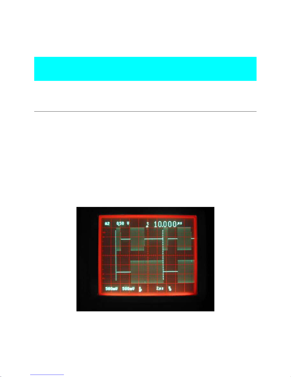
compelling price/performance proposition unmatched by any other device on the market today. Figure 1
presents sample capabilities of the board.
Figure 1: Sample PulseBlasterDDS output capabilities
www.spincore.com
9/20/20055
Page 6
PulseBlasterDDS
DAC
RF
Outputs
(SMA)
Phase0-15
Gate
Numerically
Conrolled
Oscillator
DAC
Gate
Phase0-15
Freq0-15
Reference Clock
Oscillator
Precision Timing Processor Output and Control Register
TTL
Outputs
(DB-25)
SRAM
Host Programming Interface
User Control
PulseBlasterDDS-III
© 2004 SpinCore Technologies, Inc.
http://www.spincore.com
Gate
DAC
DDS Core
Pulse Timing
Core
Tx
Rx
Board Architecture
Block Diagram
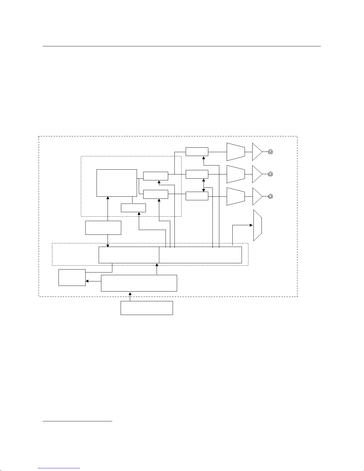
Figure 2 presents the general architecture of the PulseBlasterDDS system. The two major building
blocks are the DDS Core and the Pulse Programming and Timing Processor Core (PP Core). The
DDS Core contains a numerically controlled oscillator and has 16 programmable frequency registers
that are under the pulse program control. Prior to gating, the DDS signal can be phase offset by one of
two sets of 16 programmable phase registers. The PP Core controls the timing of the gating pulses
and provides the necessary control signals for frequency and phase registers. The DDS and PP cores
have been integrated onto a single silicon chip. High performance DAC chips and high current output
amplifiers complement the design. User control to the system is provided through the hostprogramming interface over the PCI bus.
Output signals
The PulseBlasterDDS comes with three analog output channels configured to output radio-frequency
(RF/IF) pulses, and 10 digital output signal lines (one of the output lines has a dual use and
functions as a phase reset for the DDS generator). The frequency and phase of the RF pulses generated
by the DDS are under the control of the user and are specified through software programming. The phase
of the numerically controlled oscillator can be reset on demand within the pulse program.
PulseBlasterDDS provides the ability to gate the output of the DDS channels allowing for independent
pulsed RF operation. With digital sampling rate of 100 MHz (max. reference clock frequency), the
maximum theoretical output frequency is 50 MHz (the Nyquist Theorem). 1 The analog output signal is
available on an on-board SMA connector. The output impedance of the analog signal is 50-ohms. There
are no interpolating filters on board.
1
Note that the usefulness of a waveform with two samples per period is limited, and, depending on applications,
practical considerations would often call for more than two samples per period.
www.spincore.com
Figure 2: PulseBlasterDDS board architecture
9/20/20056
Page 7

PulseBlasterDDS
The 10 individually controlled digital (TTL/CMOS) output bits are capable of delivering ±25 mA per
bit and have an output voltage of 3.3V. These signals are available on the PC bracket-mounted DB-25
connector. Setting output bit 10 high via the output control word also resets the phase of the RF
waveforms for phase coherent switching, and can be used to generate a constant voltage on the
DACs.
Timing characteristics
PulseBlasterDDS’s timing controller can accept either an internal (on-board) crystal oscillator or
an external frequency source of up to 100 MHz. The innovative architecture of the timing controller
allows the processing of either simple timing instructions (delays of up to 232 = 4,294,967,296 clock
cycles), or double-length timing instructions (up to 252 clock cycles long – nearly 2 years with a 100
MHz clock!). Regardless of the type of timing instruction, the timing resolution remains constant for
any delay – just one clock period (e.g., 10 ns for a 100 MHz clock).
The timing controller has a very short minimum delay cycle – only nine clock periods. This
translates to a 90 ns minimum pulse/delay/update with a 100 MHz clock.
Phase Coherent Switching
The board allows for phase continuous and/or phase coherent switching. In addition, the DDS
can be reset to zero whenever a new RF pulse is started. Consult the explanation of the flags
parameter to the pb_inst instruction on page 12 for implementing the phase reset.
Instruction set
PulseBlasterDDS’ design features a set of commands for highly flexible program flow control. The
micro-programmed controller allows for programs to include branches, subroutines, and loops at up to
8 nested levels – all this to assist the user in creating dense pulse programs that cycle through
repetitious events, especially useful in numerous multidimensional spectroscopy and imaging
applications.
External triggering
PulseBlasterDDS can be triggered and/or reset externally via dedicated hardware lines. The two
separate lines combine the convenience of triggering (e.g., in cardiac gating) with the safety of the
"stop/reset" line. The required control signals are “active low” (or short to ground).
Status Readback
The status of the program can be read in hardware or software. The hardware status output
signals consist of five IDC connector pins labeled “Status”. The same output can be read through
software using C. See section IV (Connecting to the PulseBlaster Board, page 16) for more detail
about the hardware lines and section III (Programming the PulseBlaster, page 11) for more detail
about the C function status_readback().
Summary
PulseBlasterDDS is a versatile, high-performance pulse/pattern TTL and RF/IF generator
operating at speeds of up to 100 MHz and capable of generating pulses/delays/intervals ranging from
90 ns to over 2 years per instruction. It can accommodate pulse programs with highly flexible control
commands of up to 32k program words. Its high-current output logic bits are independently controlled
with a voltage of 3.3 V. The output impedance of the analog channel is 50-ohms.
www.spincore.com
9/20/20057
Page 8

Specifications
DDS Specifications
• 100 MHz reference clock oscillator (other frequencies available upon request)
• 0.047 Hz frequency resolution (32 bits)
• 16 loadable frequency registers for agile frequency modulation/switching/selection (32 bits
each)
• Two sets of 16 loadable phase-offset registers for agile phase modulation/switching/selection
(12 bits each)
• 0.09° phase resolution (12 bits)
• 40 ns phase switching latency
• 40 ns frequency switching latency (phase continuous)
• phase coherent switching
• 10 dBm RF output power
• 50 ohm output impedance
• SMA connectors
• 30 MHz 3dB bandwidth
• RF Output capable of outputting DC at programmed output level (using phase offset)
TTL Specifications
• 10 individually controlled digital output lines (TTL levels; one of the output lines has a dual use
and functions as a phase reset for the DDS generator)
• variable pulses/delays for every TTL line
• 25 mA output current per TTL line
• output lines can be combined to increase the max. output current
Common Parameters (DDS and TTL Specifications)
PulseBlasterDDS
• 90 ns shortest pulse/interval per instruction
• 2 years longest pulse/interval per instruction
• 10 ns pulse/interval resolution
• RF and TTL pulses are synchronized
• 32k max. memory space
• external triggering and reset – TTL levels
Pulse Program Control Flow (Common)
• loops, nested 8 levels deep
• 20 bit loop counters (max. 1,048,576 repetitions)
• subroutines, nested 8 levels deep
• wait for trigger - 80 ns latency, adjustable to 2 years in duration
• Approximately 2 MHz max. re-triggering frequency (based on the latency of the WAIT opcode)
www.spincore.com
9/20/20058
Page 9
PulseBlasterDDS
II. Installation
Installing the PulseBlasterDDS Driver
1. Go to http://www.pulseblaster.com/CD/PulseBlasterDDS/PCI/SP3 and download sp3.zip.
2. Unzip the files to their own directory.
3. Turn off your computer.
4. Insert the PulseBlasterDDS board into an empty PCI slot. Secure the bracket firmly with a screw.
5. Turn on your computer.
For Windows XP
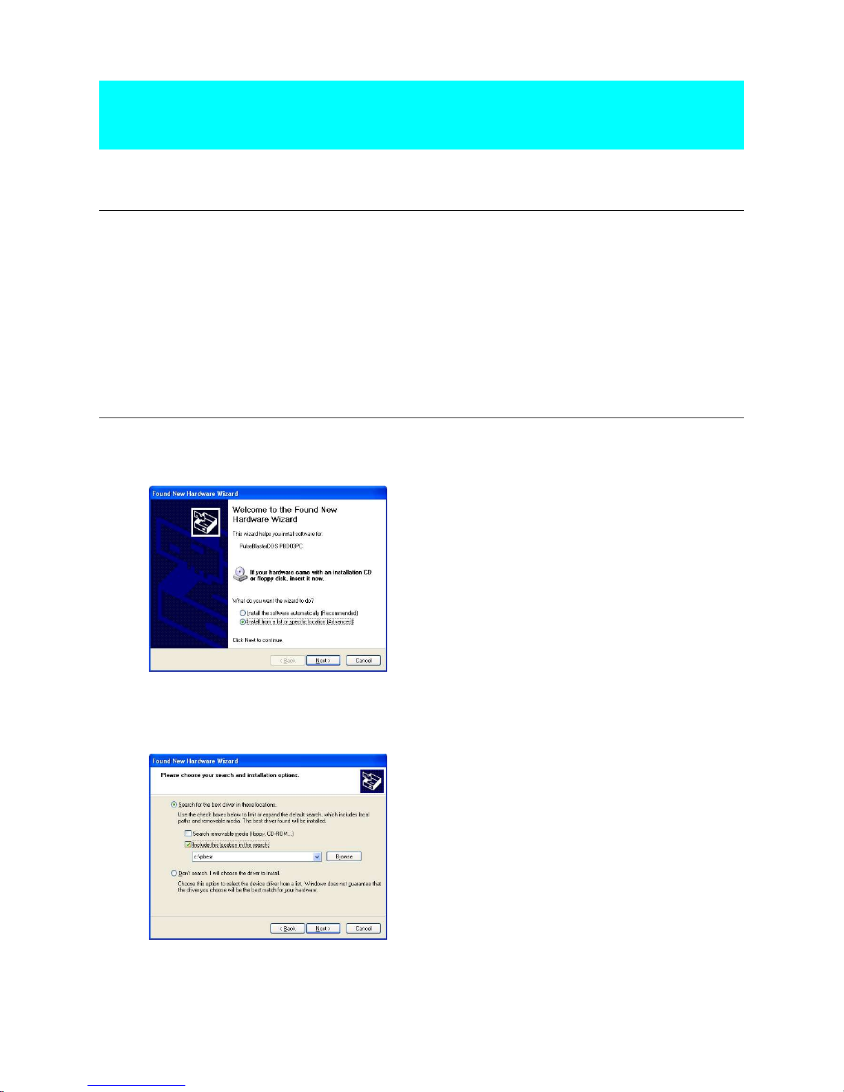
6. After booting, the “Found New Hardware Wizard” should appear. Choose “Install from a list or specific
location” and click Next
7. Choose “Include this location in the search” and browse to the directory you unzipped the drivers to.
Click next.
www.spincore.com
9/20/20059
Page 10
PulseBlasterDDS
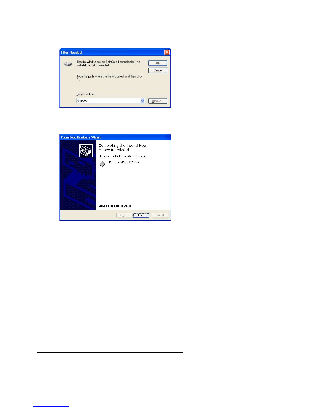
8. While windows installs the driver, a “Files Needed” dialog may pop up. Choose the directory you
unzipped the drivers to, and click ok.
9. When finished, you should see this window.
NOTE: On some systems after you install your PulseBlasterDDS board you may need to run “Install.bat”
located in the “post_installation_files.zip” file located at
http://www.pulseblaster.com/CD/PulseBlasterDDS/PCI/SP3/old_version/post_installation_files.zip
in order for your board to work.
You are now ready to control the PulseBlasterDDS board
Initializing Control of the PulseBlasterDDS
3. Run the included “SP3_Test.exe”.
If equipped with a 100 MHz reference clock oscillator, the board should now output a 6.250MHz sine
wave on the SMA connectors labeled “DAC_OUT_0”, “DAC_OUT_1”, and “DAC_OUT_2”. The 10
TTL output lines should toggle every second.
The PulseBlasterDDS board is now ready for use!
www.spincore.com
9/20/200510
Page 11

PulseBlasterDDS
III. Programming the PulseBlasterDDS
Instruction Set Architecture
Machine-Word Definition
The PulseBlaster pulse timing and control processor implements an 80-bit wide Very Long
Instruction Word (VLIW) architecture. The VLIW memory words have specific bits/fields dedicated to
specific purposes, and every word should be viewed as a single instruction of the micro-controller.
The maximum number of instructions that can be loaded to on-board memory is 32k. The execution
time of instructions can be varied and is under (self) control by one of the fields of the instruction word
– the shortest being five clock cycles (for 512 memory-word models) and the longest being 2^52 clock
cycles. All instructions have the same format and bit length, and all bit fields have to be filled. Figure
3 shows the fields and bit definitions of the 80-bit instruction word.
Bit Definitions for the 80-bit Instruction Word (VLIW)
Output/Control Word | Data Field | OP Code | Delay Count
(24 bits) (20 bits) (4 bits) (32 bits)
Figure 3: Bit definitions of the 80-bit instruction/memory word
Breakdown of 80-bit Instruction Word
The 80-bit VLIW is broken up into 4 sections
1. Output Pattern and Control Word - 24 bits
2. Data Field - 20 bits
3. OP Code - 4 bits
4. Delay Count - 32 bits
Output Pattern and Control Word
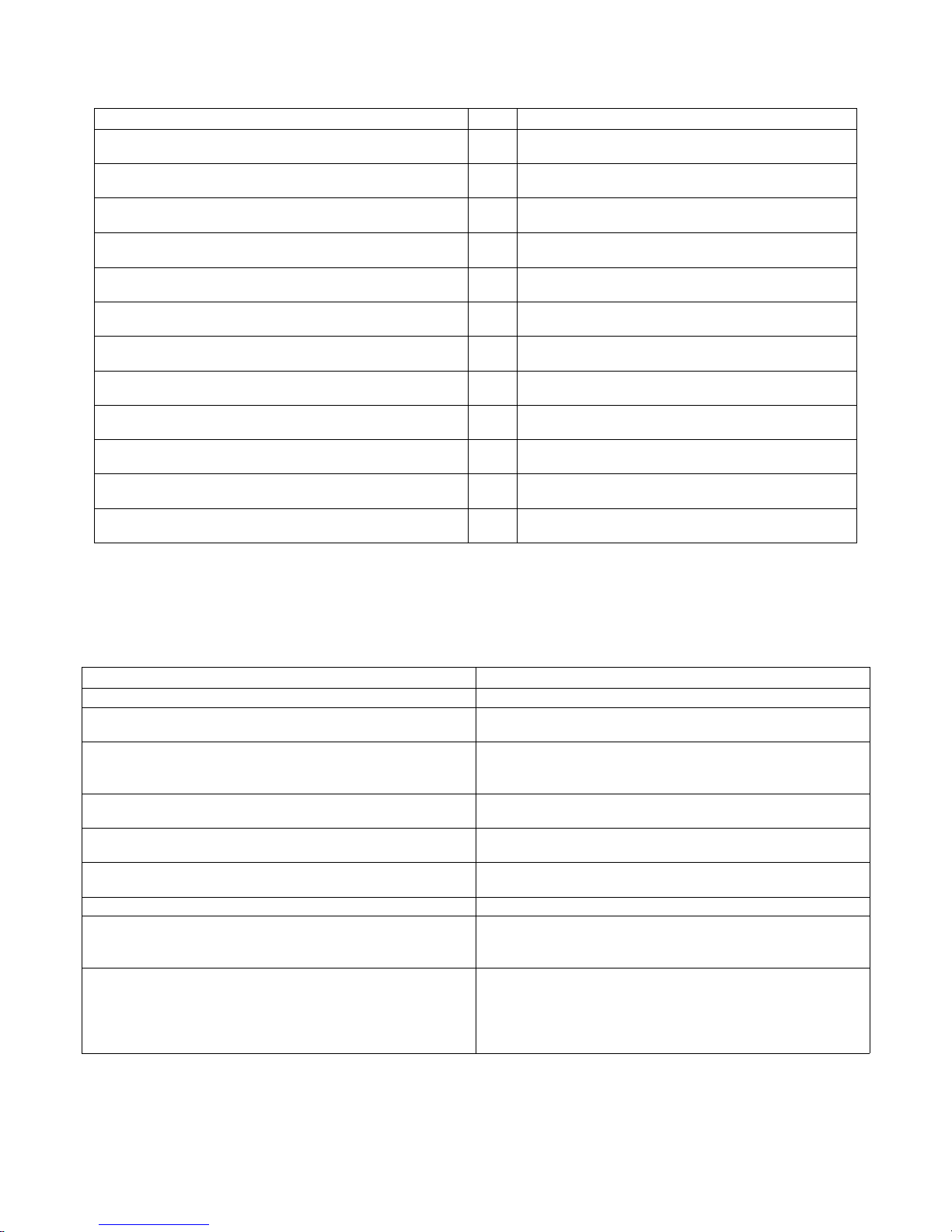
Please refer to Table 1, next page, for output pattern and control bit assignments of the 24-bit
output/control word.
www.spincore.com
9/20/200511
Page 12
PulseBlasterDDS
Bit # Function Bit # Function
23 Selects Frequency Register (bit 3) 11
22 Selects Frequency Register (bit 2) 10
21 Selects Frequency Register (bit 1) 9
20 Selects Frequency Register (bit 0) 8 Output Connector DB25 pin 7
19
18
17
16
15
14
13
12
Selects Phase Register for SMA connector
labeled DAC_OUT_1 (bit 3)
Selects Phase Register for SMA connector
labeled DAC_OUT_1 (bit 2)
Selects Phase Register for SMA connector
labeled DAC_OUT_1 (bit 1)
Selects Phase Register for SMA connector
labeled DAC_OUT_1 (bit 0)
Output Enable for SMA connector labeled
DAC_OUT_2 (0 = on, 1 = off)
Selects Phase Register for SMA connectors
labeled DAC_OUT_2 and DAC_OUT_0 (bit 3)
Selects Phase Register for SMA connectors
labeled DAC_OUT_2 and DAC_OUT_0 (bit 2)
Selects Phase Register for SMA connectors
labeled DAC_OUT_2 and DAC_OUT_0 (bit 1)
Table 1: Output Pattern and Control Word Bits
7 Output Connector DB25 pin 8
6 Output Connector DB25 pin 21
5 Output Connector DB25 pin 22
4 Output Connector DB25 pin 10
3 Output Connector DB25 pin 11
2 Output Connector DB25 pin 24
1 Output Connector DB25 pin 25
0 Output Connector DB25 pin 13
Selects Phase Register for SMA connectors
labeled DAC_OUT_2 and DAC_OUT_0 (bit 0)
Output Enable for SMA connectors labeled
DAC_OUT_1 and DAC_OUT_0 (0 = on, 1 = off)
RF phase reset for phase coherent switching,
also routed to Output Connector DB25 pin 19
Data Field and Op Code
Please refer to Table 2 for information on the available operational codes (OpCode) and the
associated data field functions (the data field's function is dependent on the Op Code)
Op Code Instruction Data Field Function
0 CONTINUE Ignored Program execution continues to next instruction
1 STOP Ignored
Number of desired loops.
2 LOOP
3 END_LOOP
4 JSR
5 RTS Ignored
6 BRANCH Address of next instruction Program execution continues at specified instruction
7 LONG_DELAY
8 WAIT Ignored
This value must be greater
than or equal to 1.
Address of beginning of
loop
Address of first subroutine
instruction
Number of desired loops.
This value must be greater
than or equal to 2.
Table 2: Op Code and Data Field Description
Stop execution of program (*Note all TTL values remain
from previous instruction, and analog outputs turn off)
Specify beginning of a loop. Execution continues to next
instruction. Data used to specify number of loops
Specify end of a loop. Execution returns to begging of
loop and decrements loop counter.
Program execution jumps to beginning of a subroutine
Program execution returns to instruction after JSR was
called
For long interval instructions. Data field specifies a
multiplier of the delay field. Execution continues to next
instruction
Program execution stops and waits for software or
hardware trigger. Execution continues to next instruction
after receipt of trigger. The latency is equal to the delay
value entered in the WAIT instruction line plus a fixed
delay of 6 clock cycles.
Delay Count
www.spincore.com
9/20/200512
Page 13

PulseBlasterDDS
The value of the Delay Count field (a 32-bit value) determines how long the current instruction should
be executed. The allowed minimum value of this field is 0x6 for the 32k memory models. The timing
controller has a fixed delay of three clock cycles and the value that one enters into the Delay Count field
should account for this inherent delay.
Using C Functions to Program the PulseBlasterDDS
A series of functions have been written to control the board and facilitate the construction of pulse
program instructions. The functions also allow the programmer to set the DDS frequency and phase
registers.
In order to use these functions, the DLL (pbd03pc.dll), the library file (pbd03pc.lib), the header files
(pbd03pc.h and pbdfuncs.h), and source file (pbdfuncs.cpp) must be in the working directory of your C
compiler2.
int pb_init();
Initializes PulseBlasterDDS board. Needs to be called before calling any functions using the
PulseBlasterDDS. Returns a negative number on an error or 0 on success.
int pb_close();
Releases PulseBlasterDDS board. Needs to be called as last command in pulse program.
Returns a negative number on an error or 0 on success.
void set_clock(double clock_freq);
Used to set the clock frequency of the board. The variable clock_frequency is specified in MHz
when no units are entered. Valid units are MHz, kHz, and Hz. The default clock value is 50MHz.
You only need to call this function if you are not using a 50MHz board.
int start_programming(int device);
Used to initialize the system to receive programming information. It accepts a parameter
referencing the target for the instructions. Valid values for device are PULSE_PROGRAM,
FREQ_REGS, PHASE_REGS_0, and PHASE_REGS_1. PHASE_REGS_0 programs the phase
registers for the DDS output on SMA connectors labeled DAC_OUT_0 and DAC_OUT_2.
PHASE_REGS_1 programs the phase registers for the DDS output on SMA connector labeled
DAC_OUT_1. The function returns a 0 on success or a negative number on an error.
int set_freq(double freq);
Used to set the values in the frequency registers. Should only be called after start_programming
(FREQ_REGS) has been called. Registers are programmed one at a time, starting at 0 and
incrementing each time this function is called. It accepts the value for the frequency register with
a default unit of MHz. Valid units are MHz, kHz, Hz. It returns a 0 on success or a negative
number on an error.
int set_phase(double phase);
Used to set the values in the phase registers. Should only be called after start_programming
(PHASE_REGS_0) or start_programming(PHASE_REGS_1) has been called. Registers are
programmed one at a time, starting at 0 and incrementing each time this function is called. It
accepts the value for the phase register in degrees. It returns a 0 on success or a negative
number on an error.
int pb_inst(int freq, int phase_SMA_1, int tx_output_enable,
int phase_SMA_0, int rx_output_enable, int flags, int inst,
2
These functions and library files have been generated and tested with the MS Visual Studio 6 environment. Support and updated
functions/DLLs for other environments may be provided upon request if available.
www.spincore.com
9/20/200513
Page 14

PulseBlasterDDS
int inst_data, double length);
Used to send one instruction of the pulse program. Should only be called after
start_programming(PULSE_PROGRAM) has been called. It returns a negative number on an
error, or the instruction number upon success. If the function returns –99, an invalid parameter
was passed to the function. Instructions are numbered starting at 0.
int freq – Selects the frequency register to be used. Valid range is from 0 to 16
int phase_SMA_1 – Selects the phase register to be used from the phase registers programmed
using start_programming(PHASE_REG_1). This is the DDS output on SMA connector labeled
DAC_OUT_1. Valid range is from 0 to 16
int tx_output_enable – Determines whether analog output is generating a sinusoid or is at
ground for TX output on SMA connector labeled DAC_OUT_2. Valid values are
TX_ANALOG_ON and TX_ANALOG_OFF
int phase_SMA_0 – Selects the phase register to be used from the phase registers programmed
using start_programming(PHASE_REG_0). This is the DDS output on SMA connectors labeled
DAC_OUT_0 and DAC_OUT_2. Valid range is from 0 to 16
int rx_output_enable – Determines whether analog output is generating a sinusoid or is at
ground for RX output on SMA connectors labeled DAC_OUT_0 and DAC_OUT_1. Valid values
are RX_ANALOG_ON and RX_ANALOG_OFF
int flags – determines state of each TTL output bit. Valid values are 0x0 to 0x3FF. For example,
0x010 would correspond to bit 5 being on and all other bits being off. Bit 10, corresponding to
hexadecimal value 0x200, is used to reset the phase of the numerically controlled oscillator. This
results in phase coherent switching. The numerical oscillator will pause for the length of the
instruction, resulting in a constant voltage at the DAC. The voltage level depends on the value of
the phase register in use.
int inst – determines which type of instruction is to be executed. Please see Table 2 for details.
int inst_data – data to be used with the previous inst field. Please see Table 2 for details.
double length – duration of this pulse program instruction, specified in ns.
This function has been overloaded to accommodate TTL-only programs. When using the shorter
version of the function, the RF channel has its output set to ground. The overloaded form follow:
TTL Only:
int pb_inst(int flags, int inst, int inst_data, double length);
int stop_programming();
Used to tell that programming the board is complete. Board execution cannot start until this
command is received. It returns a 0 on success or a negative number on an error.
int start_pb();
Once board has been programmed, this instruction will start execution of pulse program. It
returns a 0 on success or a negative number on an error.
int stop_pb();
Stops output of board. Analog output will return to ground, and TTL outputs will remain in the
state they were in when stop command was received. It returns a 0 on success or a negative
number on an error.
www.spincore.com
9/20/200514
Page 15

PulseBlasterDDS
int status_readback();
Reads the status of the board and returns an integer whose bit representation corresponds to the
status signals described in section IV. Bit zero is stopped; bit one is reset; bit two is running; bit
three is waiting.
Example Use of C Functions
// Example1.cpp
//
// SpinCore Technologies, Inc.
// May 2004
// http://www.spincore.com
//
// The following program code uses C Functions from 'pbdfuncs' to
// generate and execute a pulse sequence on the PulseBlasterDDS board.
// Be sure to include the DLL (pbd03pc.dll), the library file
// (pbd03pc.lib), the header files (pbd03pc.h and pbdfuncs.h), and source
// file (pbdfuncs.cpp) in the working directory of your C compiler .
#include "pbdfuncs.h"
#include "pbdfuncs.cpp"
#include "PBD03PC.h"
#include <stdio.h>
void main(void)
{
int start;
// Locates & Initializes the PulseBlasterDDS Board
pb_init();
// Set Because the Board Operates at 100MHz
set_clock(100);
// Prepare the Board to Receive Freqeuncy Values
start_programming(FREQ_REGS);
// Load Frequency Register 0
set_freq(1.054);
// Load Frequency Register 1
set_freq(2);
// Prepare the Board to Receive TX Phase Values
start_programming(PHASE_REGS_1);
// Load Phase Register 0
set_phase(0);
// Load Phase Register 1
set_phase(90);
// Prepare the Board to Receive RX Phase Values
start_programming(PHASE_REGS_0);
// Load Phase Register 0
set_phase(0);
// Load Phase Register 1
set_phase(180);
// Prepare the Board to Receive pulse program instructions
start_programming(PULSE_PROGRAM);
//Instruction 0 - Continue to instruction 1 in 2us
//Freq Reg 0, Phase Reg 1 for DAC_OUT_1, DDS TX Output ON, Phase Reg 0 for
//DAC_OUT_0 and DAC_OUT_2, DDS RX Output ON, Flags = 0x3FF, OPCODE = CONTINUE
start = pb_inst(0, 1, TX_ANALOG_ON, 0, RX_ANALOG_ON, 0x3FF, CONTINUE, 0, 2*us);
// Instruction 1 - Continue to instruction 2 in 4us
//Freq Reg 0, Phase Reg 1 for DAC_OUT_1, DDS TX Output OFF, Phase Reg 0 for
//DAC_OUT_0 and DAC_OUT_2, DDS RX Output ON, Flags = 0x000, OPCODE = CONTINUE
www.spincore.com
9/20/200515
Page 16

PulseBlasterDDS
pb_inst(0, 1, TX_ANALOG_OFF, 0, RX_ANALOG_ON, 0x000, CONTINUE, 0, 4*us);
// Instruction 2 - Branch to "start" (Instruction 0) in 2us
//Freq Reg 0, Phase Reg 1 for DAC_OUT_1, DDS TX Output ON, Phase Reg 0 for
//DAC_OUT_0 and DAC_OUT_2, DDS RX Output ON, Flags = 0x000, OPCODE = BRANCH
pb_inst(0, 1, TX_ANALOG_ON, 0, RX_ANALOG_ON, 0x000, BRANCH, start, 2*us);
// Finished Sending Instructions
stop_programming();
// Run the Program
start_pb();
// Release Control of the PulseBlasterDDS Board
pb_close();
}
A more complex program using C Functions is provided in Appendix I.
www.spincore.com
9/20/200516
Page 17
PulseBlasterDDS
IV. Connecting to the PulseBlasterDDS Board
Connector Information
SMA Connectors labeled DAC_OUT_0, DAC_OUT_1, and DAC_OUT_2
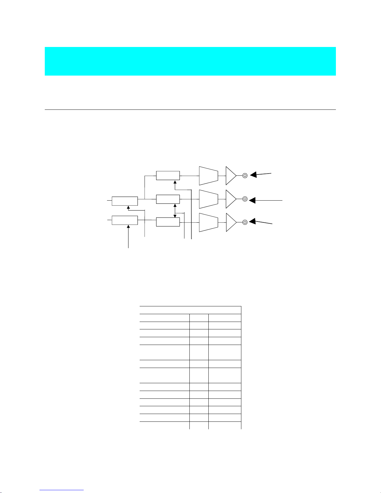
Outputs DDS signals generated by the user’s Program. The output impedance is 50 ohms.
Output power is approximately 10 dBm. Figure 4 is a portion of figure 2 that illustrates which RF output
corresponds to which SMA connector.
Phase0-15
Gate
Gate
Tx
DAC
RF
Outputs
DAC
DAC_OUT_2
(SMA)
DAC_OUT_0
Rx
Phase0-15
Gate
DAC
Figure 4: SMA Connectors
DAC_OUT_1
DB-25 - TTL Output Signal Bits
Outputs TTL signals generated by the user’s Program. Please consult the table below for bit
assignments.
Pin Assignments
Pin# Bit# Pin# Bit#
1 GND 14 GND
2 Reserved 15 Reserved
3 GND 16 Reserved
4 Reserved 17 GND
5 Reserved 18 Reserved
6 GND 19 9
7 8 20 GND
8 7 21 6
9 GND 22 5
10 4 23 GND
11 3 24 2
12 GND 25 1
13 0
Table 3: Output bits and signals of the PulseBlasterDDS board
www.spincore.com
9/20/200517
Page 18
PulseBlasterDDS
IDC Connector Status - Pin Assignments
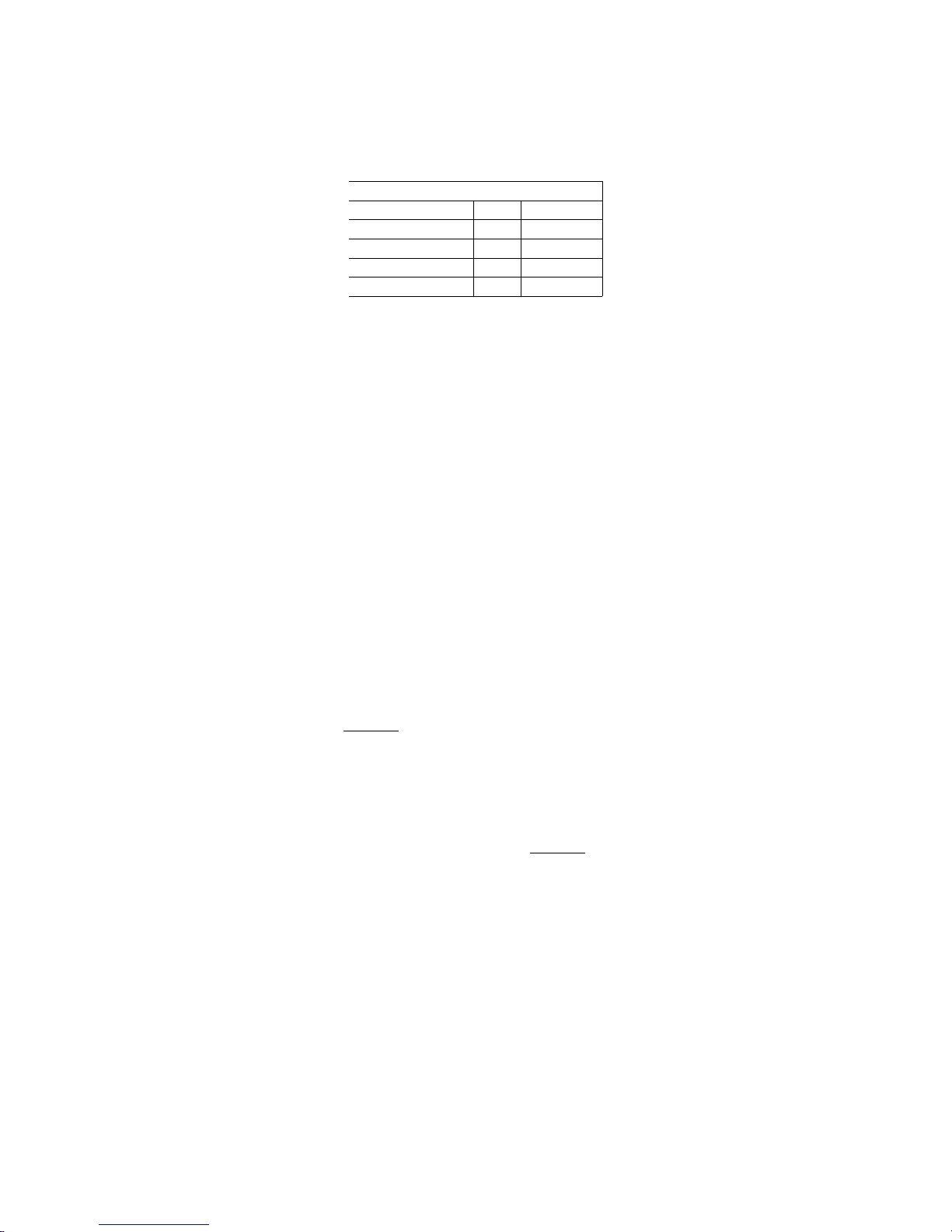
The IDC connector labeled Status outputs TTL signals based on status of the user’s program.
Please consult the table below for pin assignments.
Pin Assignments
Pin# Pin#
1 Stopped 5 Running
2 GND 6 GND
3 Reset 7 Waiting
4 GND 8 GND
Table 4: Status signals of the PBDDS-III
The status pins correspond to the current state of the pulse program and are defined as follows:
Stopped – Driven high when the PulseBlaster device has encountered a STOP Op Code during program
execution and has entered a stopped state.
Reset – Driven high when the PulseBlaster device is in a RESET state and must be reprogrammed before
code execution can begin again.
Running – Driven high when the PulseBlaster device is executing a program. It is low when the
PulseBlaster enters either a reset or idle state.
Waiting – the PulseBlaster device has encountered a WAIT Op Code and is waiting for the next trigger
(either hardware or software) to resume operation.
Header JP100
This is an input connector, for hardware triggering (HW_Trigger) and resetting (HW_Reset).
HW_Trigger is pulled high by default, and pin 1 is active (pin 2 = GND). When a low state is
detected (e.g., when shorting pins 1-2), it initiates code execution. This trigger will also restart
execution of a program from the beginning of the code if it is detected after the design has reached an
idle state. The idle state could have been created either by reaching the STOP Op Code of a
program, or by the detection of the HW_Reset signal. When the WAIT Op Code is used in the pulse
program, the HW_Trigger will cause the program to continue to the next instruction.
HW_Reset is pulled high by default, and pin 3 is active (pin 4 = GND). It can be used to halt the
execution of a program by pulling it low (e.g., by shorting pins 3-4). When the signal is pulled low
during the execution of a program, the controller resets itself back to the beginning of the program.
Program execution can be resumed by either a software start command or by a hardware trigger.
SMA Connector labeled “SMA0”
This SMA connector outputs the reference clock as a 3.3 V TTL signal, i.e., it generates positive-
only voltage. The output resembles a square wave if properly terminated. This signal can be
measured with an oscilloscope using either a high impedance probe at the SMA connector or a 50
ohm coaxial line that is terminated.
SMA Connector labeled “SMA400”
www.spincore.com
9/20/200518
Page 19

PulseBlasterDDS
This SMA connector is used as an external clock input. Before attaching the external clock,
the internal clock must be removed from its socket. The internal clock’s orientation should be noted (if
the internal clock is reconnected, it must be inserted in the same orientation or board damage may
occur). Also, the external clock must be a 3.3 V TTL signal. Another requirement is that a 50 ohm
resistor be soldered directly on the board on R401 pads or use a T connector with a 50 ohm terminator
connected directly to SMA400. Failure to follow the above requirements could result in damaging the
board.
Appendix I: Sample C program
Example Program
// Example2.cpp
//
// SpinCore Technologies, Inc.
// May 2004
// http://www.spincore.com
//
// The following program code uses C Functions from 'pbdfuncts' to
// generate and execute a pulse sequence on the PulseBlasterDDS board.
// Be sure to include the DLL (pbd03pc.dll), the library file
// (pbd03pc.lib), the header files (pbd03pc.h and pbdfuncs.h), and source
// file (pbdfuncs.cpp) in the working directory of your C compiler .
#include "pbdfuncs.h"
#include "pbdfuncs.cpp"
#include "PBD03PC.h"
#include <stdio.h>
void main(void)
{
if (pb_init() != 0)
printf("--- Error Initializing PulseBlasterDDS ---\n");
// Check for proper initialization of PulseBlasterDDS
// Set clock frequency
set_clock(100);
// Start programming the frequency registers
start_programming(FREQ_REGS);
// Program the registers in order from 0 to 15
// Valid units are MHz, kHz, and Hz - default is MHz
www.spincore.com
9/20/200519
Page 20

set_freq(1*MHz); // Set register 0
set_freq(2*MHz); // Set register 1
set_freq(3*MHz); // Set register 2
set_freq(4*MHz); // Set register 3
set_freq(5*MHz); // Set register 4
set_freq(6*MHz); // Set register 5
set_freq(7*MHz); // Set register 6
set_freq(8*MHz); // Set register 7
set_freq(9*MHz); // Set register 8
set_freq(10*MHz); // Set register 9
set_freq(11*MHz); // Set register 10
set_freq(12*MHz); // Set register 11
set_freq(13*MHz); // Set register 12
set_freq(14*MHz); // Set register 13
set_freq(15*MHz); // Set register 14
set_freq(16*MHz); // Set register 15
// Start programming the phase registers for DAC_OUT_1
start_programming(PHASE_REGS_0);
// Program the registers in order from 0 to 15
// Units are in degrees
set_phase(0); // Set register 0
set_phase(22.5); // Set register 1
set_phase(45); // Set register 2
set_phase(67.5); // Set register 3
set_phase(90); // Set register 4
set_phase(112.5); // Set register 5
set_phase(135); // Set register 6
set_phase(157.5); // Set register 7
set_phase(180); // Set register 8
set_phase(202.5); // Set register 9
set_phase(225); // Set register 10
set_phase(247.5); // Set register 11
set_phase(270); // Set register 12
set_phase(292.5); // Set register 13
set_phase(315); // Set register 14
set_phase(337.5); // Set register 15
PulseBlasterDDS
// Start programming the phase registers for DAC_OUT_0 and DAC_OUT_2
start_programming(PHASE_REGS_1);
// Program the registers in order from 0 to 15
// Units are in degrees
set_phase(0); // Set register 0
set_phase(22.5); // Set register 1
set_phase(45); // Set register 2
set_phase(67.5); // Set register 3
set_phase(90); // Set register 4
set_phase(112.5); // Set register 5
set_phase(135); // Set register 6
set_phase(157.5); // Set register 7
set_phase(180); // Set register 8
set_phase(202.5); // Set register 9
set_phase(225); // Set register 10
set_phase(247.5); // Set register 11
set_phase(270); // Set register 12
set_phase(292.5); // Set register 13
set_phase(315); // Set register 14
set_phase(337.5); // Set register 15
//Begin pulse program
start_programming(PULSE_PROGRAM);
www.spincore.com
9/20/200520
Page 21

PulseBlasterDDS
int start, loop, sub; // define instruction labels
sub = 5; // Since we are going to jump forward in our program, we need to
// define this variable by hand. Instructions start at 0 and count up
// Instruction 0 - Jump to Subroutine at Instruction 5 in 1us
start = pb_inst(0,0,TX_ANALOG_ON,0,RX_ANALOG_ON,0x3FF,JSR,sub,1*us);
// Instruction 1 - Beginning of Loop (Loop 3 times). Continue to next
instruction in 1us
loop = pb_inst(0,0,TX_ANALOG_OFF,0,RX_ANALOG_OFF,0x0,LOOP,3,1*us);
// Instruction 2 - End of Loop. Return to beginning of loop or continue to
next instruction in 1us
pb_inst(0,0,TX_ANALOG_ON,0,RX_ANALOG_OFF,0x0,END_LOOP,loop,1*us);
// Instruction 3 - Stay here for (5*1us) then continue to Instruction 4
pb_inst(0,0,TX_ANALOG_OFF,0,RX_ANALOG_ON,0x0,LONG_DELAY,5,1*us);
// Instruction 4 - Branch to "start" (Instruction 0) in 1us
pb_inst(0,0,TX_ANALOG_OFF,0,RX_ANALOG_ON,0x0,BRANCH,start,1*us);
// Instruction 5 - Continue to next instruction in 2us
pb_inst(0,4,TX_ANALOG_OFF,8,RX_ANALOG_ON,0x0,CONTINUE,0,2*us);
// Instruction 6 - Return from Subroutine to Instruction 1 in 2us
pb_inst(0,8,TX_ANALOG_OFF,8,RX_ANALOG_ON,0x0,RTS,0,2*us);
// End of programming registers and pulse program
stop_programming();
// Start execution of the pulse program
start_pb();
// Release control of the PB board
pb_close();
}
www.spincore.com
9/20/200521
Page 22

PulseBlasterDDS
Appendix II: Programming the
PulseBlasterDDS Using Direct Outputs
If you do not wish to use the provided C functions, you can take advantage of the PBD03PC_outp()
function in your own applications. An explanation of using this function to program the board is included
below.
Using DLL Functions to Send Instructions
The provided driver DLL, pbd03pc.dll, provides three functions necessary for programming the
PulseBlasterDDS:
int PBD03PC_Init();
This function locates and initializes the PulseBlasterDDS PCI board. It returns a 0 upon
successful completion, or a negative number for an error.
int PBD03PC_outp(unsigned short address, int data);
This function sends 8 bits of data to the PCI board, at a specified address offset. (Only the lowest
8 bits of the integer value are sent)
int PBD03PC_Close();
This function releases control of the PulseBlasterDDS PCI board. It returns a 0 upon successful
completion, or a negative number for an error.
Building Instructions Using the DLL Functions
• To send instructions to the PulseBlasterDDS, the programmer must first call the
PBD03PC_Init() function to locate and initialize the PulseBlasterDDS for sending
instructions
• Instructions are then build using the PBD03PC_outp(unsigned short address, int
data) function, 8 bits at a time. For example, 10 PBD03PC_outp function calls are made to
construct one 80-bit instruction in accordance with the Instruction Set Architecture
• Finally, the PBD03PC_Close() instruction is called to signal an end to programming, and to
release control of the PulseBlasterDDS
Programming Information
Initialization of the PulseBlasterDDS for operation involves a minimum of four steps. The steps are as
follows:
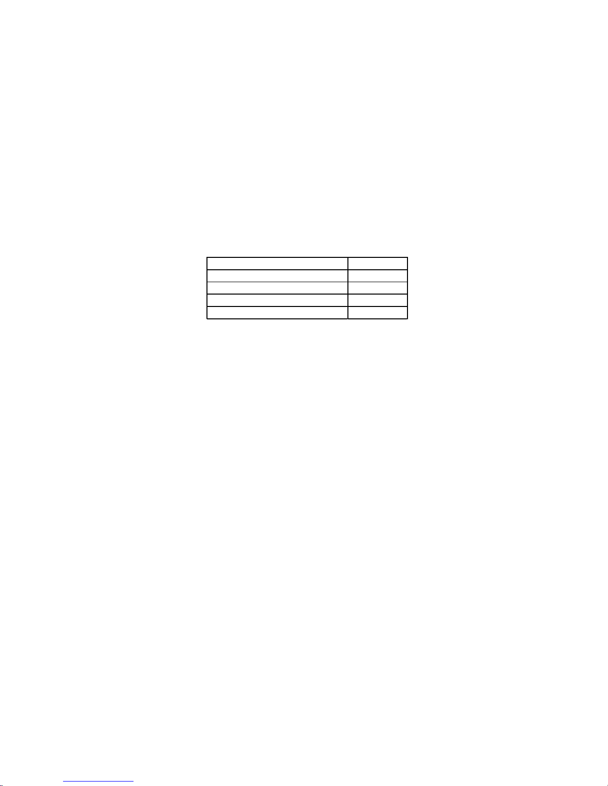
1) Send LOAD NUMBER OF BYTES PER WORD instruction.
2) Send SELECT PERIPHERAL DEVICE instruction.
3) Send CLEAR ADDRESS COUNTER instruction.
4) Loading data to memory.*
5) Send PROGRAMMING FINISHED instruction.
www.spincore.com
9/20/200522
Page 23
PulseBlasterDDS
WE Register Value (hex)
Program Memory 0
Program Frequency Registers 1
Program Phase Registers 2
Change Flags Only FF
* Once the board has been programmed, this step is optional. If you are just restarting the pulse program
after a STOP command or an HARDWARE_RESET has stopped the program, you can skip this step
during re-initialization.
If these five commands are not sent from a PC, the PulseBlasterDDS will not run as desired. All five
instructions are required as an attempt to ensure that the device has been programmed before it can be
armed. The first time the system is used, the loading of the memory with data has to be performed. Upon
reset, four instructions must be executed to restart the device again.
WE for Peripherals: This register is used to select the peripheral that is to be programmed. The
value of this register that is used to select program memory is always zero and this is the default value for
the register. A complete listing of the values and the associated hardware that can be programmed when
appropriately set is listed below in Table A1.1. By selecting 0xFF for this value, no device is selected and
the initial value of the output flags may be set. (*Note that the clock signal to the FF must still be
transitioned, which may be accomplished by writing to the base output port + 5 twice in succession.)
Table A1.1: Peripheral List
CLEAR ADDRESS COUNTER: The Address Counter is used to manufacture the memory address.
The Address Counter is not loadable; it can only be cleared and started at zero. It is not possible to load a
particular section of memory. All loads must start from either the beginning of memory, or wherever the
Address Counter left off.
Flag Initialization Strobe: The output flags of the PulseBlasterDDS can be programmed while the
device is in a reset state. This is useful to initialize flags after powering-up and to reset flags to a known
state if a program must be aborted. Writing to the Flag Initialization Strobe register will toggle the line
used to clock data into the output latches.
LOAD_MEMORY: This instruction is used to specify data that should be used to program the memory
used by the device. Since the incoming data is taken only one byte at a time, the IBC must reconstruct
the data word to be programmed. The data word is reconstructed in the IBC most significant byte first.
PROGRAMMING FINISHED: This instruction enables the pattern generator of the PulseBlasterDDS.
This instruction prevents the pattern generator from accepting a hardware trigger or software start
command before the device has been programmed. Once the design has been programmed, the
PROGRAMMING FINISIHED command must be sent to arm the device for operation. After the pattern
generator has been armed, any hardware trigger or software start command will cause the system to start
operation. The PulseBlasterDDS can be reset by issuing the DEVICE_RESET command. This will
internally clear the PROGRAMMING FINISHED instruction and prevent the pattern generator from
operating again until the IBC has been re-initialized.
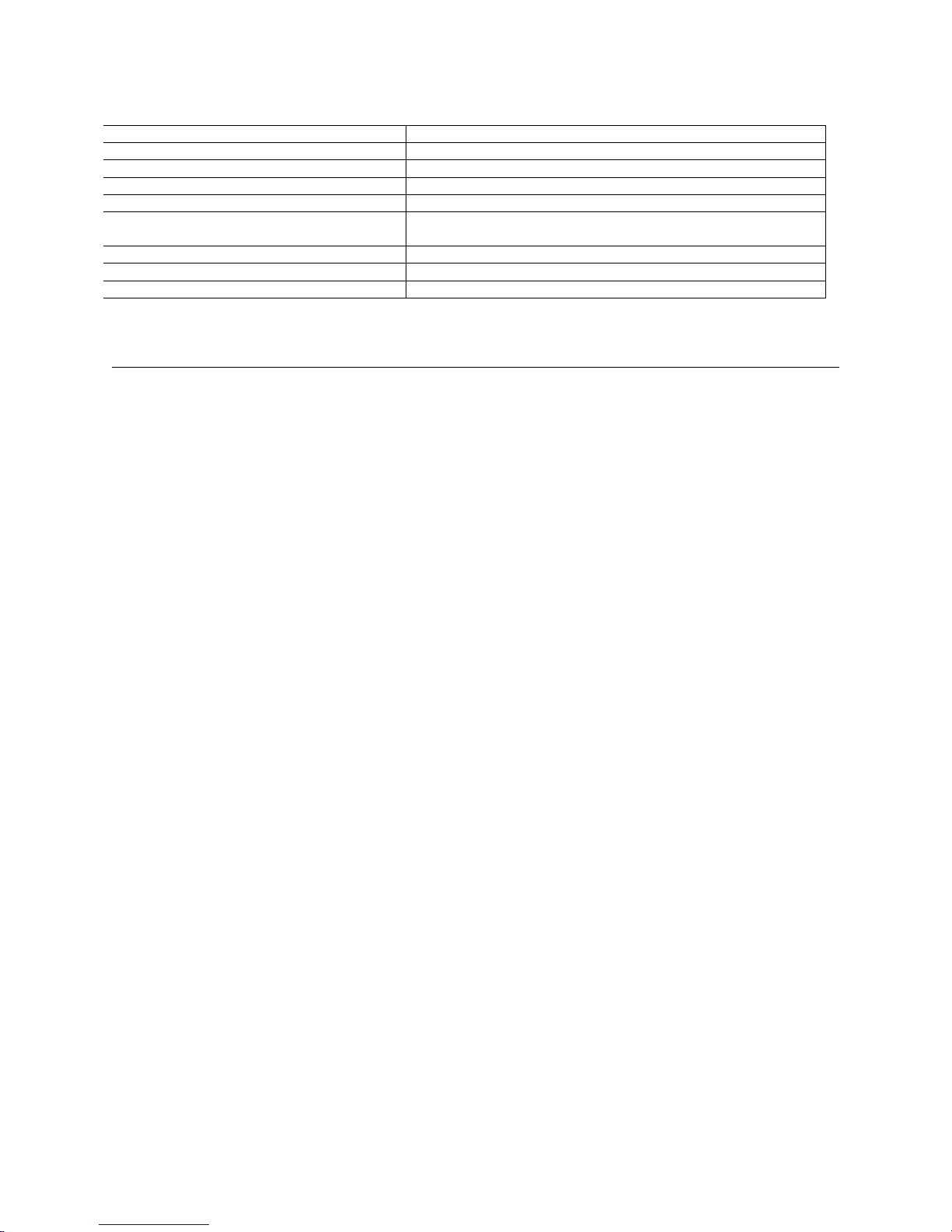
In order to select each of the commands mentioned about, you write to the port base + offset. A table of
each offset’s meaning is included below, see next page.
www.spincore.com
9/20/200523
Page 24
PulseBlasterDDS
Offset Command Function
0 DEVICE_RESET Stops Pulse Program
1 DEVICE_START Starts Pulse Program (only when in initialized state)
2 SELECT_BPW Selects number of BPW (10 for instructions)
3 SELECT_DEVICE Using Table 2, selects internal device to be programmed
4 CLEAR_ADDRESS_COUNTERResets internal memory address counter
5 FLAG_STROBE Strobes output clock signal to preset digital outputs
6 DATA_TRANSFER Data to be written to internal device
7 PROGRAMMING_FINISHED Sets device in initialized state
Table A1.2: Port Offset Command Functions
Example Program
The following is an example of the output sequence to program the PulseBlasterDDS. You must use the
PBD03PC_outp(addr, data) function from the provided DLL in order to use this method.
// Initialization:
PBD03PC_outp(0,0); //(Issue device reset)
PBD03PC_outp(2,4); //(Select number of bytes per word)
PBD03PC_outp(3,0xFF); //(Select device to program (Flag initial values))
PBD03PC_outp(4,0); //(Reset address counter)
// Set initial flag values
// Values for this example are "0x000000f0"
PBD03PC_outp(6,0); //(Data transfer)
PBD03PC_outp(6,0); //(Data transfer)
PBD03PC_outp(6,0); //(Data transfer)
PBD03PC_outp(6,0xF0); //(Data transfer)
PBD03PC_outp(5,0); //(Clock data into external buffer)
PBD03PC_outp(5,0); //(Return clock signal to low)
// Set up DDS frequency registers
PBD03PC_outp(0,0); //(Issue device reset)
PBD03PC_outp(2,4); //(Select number of bytes per word)
PBD03PC_outp(3,1); //(Select device to program (DDS Frequency Registers))
PBD03PC_outp(4,0); //(Reset address counter)
/*
*/
PBD03PC_outp(6,0x05); //(Data Transfer - Byte 3 of Reg0)
PBD03PC_outp(6,0x1E); //(Data Transfer - Byte 2 of Reg0)
PBD03PC_outp(6,0xB8); //(Data Transfer - Byte 1 of Reg0)
PBD03PC_outp(6,0x52); //(Data Transfer - Byte 0 of Reg0)
PBD03PC_outp(6,0x05); //(Data Transfer - Byte 3 of Reg1)
PBD03PC_outp(6,0x3D); //(Data Transfer – Byte 2 of Reg1)
PBD03PC_outp(6,0x70); //(Data Transfer - Byte 1 of Reg1)
PBD03PC_outp(6,0xA4); //(Data Transfer - Byte 0 of Reg1)
.
.
DDS Register Values
Reg0 = 051EB852 (1 MHz)
Reg1 = 0A3D70A4 (2 MHz)
.
.
Reg15 = 147AE148 (4 MHz)
Formula for finding these values:
REG0 = DESIRED_FREQUENCY * 232 / PBDDS_CLOCK
= 1 MHz * 232 / 50 MHz = 858993459.2 = 0x051EB852
www.spincore.com
9/20/200524
Page 25

PulseBlasterDDS
PBD03PC_outp(6,0x14); //(Data Transfer - Byte 3 of Reg15)
PBD03PC_outp(6,0x7A); //(Data Transfer - Byte 2 of Reg15)
PBD03PC_outp(6,0xE1); //(Data Transfer - Byte 1 of Reg15)
PBD03PC_outp(6,0x48); //(Data Transfer - Byte 0 of Reg15)
// Set up phase registers
PBD03PC_outp(0x0); //(Issue device reset)
PBD03PC_outp(2,4); //(Select number of bytes per word)
PBD03PC_outp(3,2); //(Select device to program (TX Phase Registers))
PBD03PC_outp(4,0); //(Reset address counter)
/*
register. The other digits must still be sent so that the DDS word remains 32 bits long.
*/
PBD03PC_outp(6,0x09); //(Data Transfer - Byte 3 of Reg0)
PBD03PC_outp(6,0x3E); //(Data Transfer - Byte 2 of Reg0)
PBD03PC_outp(6,0x93); //(Data Transfer - Byte 1 of Reg0)
PBD03PC_outp(6,0xE9); //(Data Transfer - Byte 0 of Reg0)
PBD03PC_outp(6,0x40); //(Data Transfer - Byte 3 of Reg1)
PBD03PC_outp(6,0x00); //(Data Transfer - Byte 2 of Reg1)
PBD03PC_outp(6,0x00); //(Data Transfer - Byte 1 of Reg1)
PBD03PC_outp(6,0x00); //(Data Transfer - Byte 0 of Reg1)
.
.
PBD03PC_outp(6,0xE0); //(Data Transfer - Byte 3 of Reg15)
PBD03PC_outp(6,0x00); //(Data Transfer - Byte 2 of Reg15)
PBD03PC_outp(6,0x00); //(Data Transfer - Byte 1 of Reg15)
PBD03PC_outp(6,0x00); //(Data Transfer - Byte 0 of Reg15)
// Pulse Program Setup
PBD03PC_outp(0,0); //(Issue Device Reset)
PBD03PC_outp(2,10); //(Select number of bytes per word)
PBD03PC_outp(3,0); //(Select device to program (RAM))
PBD03PC_outp(4,0); //(Reset address counter)
Phase Register Values
Reg0 = 093E93E9 (13 degrees)
Reg1 = 40000000 (90 degrees)
.
.
Reg15 = E0000000(315 degrees)
Formula for finding these values:
REG0 = DESIRED_PHASE * 232 / 360
= 13 * 2
* Note that only the top 3 hex digits (0x093) are actually used in programming the phase
32
/ 360 = 155096041.24 ≈ 0x093E93E9
//Send pulse program
PBD03PC_outp(6,0x18); //(Byte 9 of first instruction)
PBD03PC_outp(6,0xFF); //(Byte 8 of first instruction)
PBD03PC_outp(6,0xFF); //(Byte 7 of first instruction)
PBD03PC_outp(6,0x00); //(Byte 6 of first instruction)
PBD03PC_outp(6,0x00); //(Byte 5 of first instruction)
PBD03PC_outp(6,0x00); //(Byte 4 of first instruction)
PBD03PC_outp(6,0x00); //(Byte 3 of first instruction)
PBD03PC_outp(6,0x00); //(Byte 2 of first instruction)
PBD03PC_outp(6,0x00); //(Byte 1 of first instruction)
PBD03PC_outp(6,0x07); //(Byte 0 of first instruction)
PBD03PC_outp(6,0xXX); //(Byte 9 of second instruction)
/*
Continue this process for all instructions. The
explanation of how to create the 80 bit instruction
words is included above. When finished with all
instructions, continue with the sequence below.
*/
PBD03PC_outp(7,0); //(Programming Finished)
www.spincore.com
9/20/200525
Page 26

/*
Only execute the following command when you are ready
for the program to start running.
*/
PBD03PC_outp(1,0); //(Start pulse program)
PulseBlasterDDS
www.spincore.com
9/20/200526
Page 27

Contact Information
Phone (352) 271-7383
FAX (352) 371-8679
Email [email protected]
Web http://www.spincore.com/
Product URL:
http://www.pulseblaster.com/CD/PulseBlasterDDS/PCI/SP3
PulseBlasterDDS
www.spincore.com
9/20/200527
 Loading...