

Page 1
PulseBlasterDDS™
Model DDS-I-300
(USB Board Version SP7)
Owner’s Manual
SpinCore Technologies, Inc.
http://www.spincore.com
Page 2

PulseBlasterDDS-I-300
Congratulations and thank you for choosing a design from SpinCore
Technologies, Inc.
We appreciate your business!
At SpinCore we try to fully support the needs of our customers. If you are in
need of assistance, please contact us and we will strive to provide the
necessary support.
© 2007 - 2017 SpinCore Technologies, Inc. All rights reserved.
SpinCore Technologies, Inc. reserves the right to make changes to the product(s) or information herein without notice.
PulseBlasterDDS™, PulseBlaster™, SpinCore, and the SpinCore Technologies, Inc. logos are trademarks of SpinCore Technologies, Inc. All other
trademarks are the property of their respective owners.
SpinCore Technologies, Inc. makes every effort to verify the correct operation of the equipment. This equipment version is not intended for use in a
system in which the failure of a SpinCore device will threaten the safety of equipment or person(s).
http://www.spincore.com 2 2017-11-14
Page 3

PulseBlasterDDS-I-300
Table of Contents
Table of Contents ................................................................................................................................... 3
I. Introduction ......................................................................................................................................... 4
Product Overview ....................................................................................................................................................... 4
Board Architecture ...................................................................................................................................................... 4
Block Diagram ....................................................................................................................................................... 4
Product Specifications ................................................................................................................................................ 6
RF Output Level ........................................................................................................................................................... 7
II. Installation .......................................................................................................................................... 8
Installing the PulseBlasterDDS-I-300 ......................................................................................................................... 8
Testing the PulseBlasterDDS-I-300 ............................................................................................................................. 9
III. Using the PulseBlasterDDS-I-300 ................................................................................................. 11
Controlling the PulseBlasterDDS-I-300 with SpinAPI .............................................................................................. 11
Frequency and Phase Registers ............................................................................................................................... 11
Sample Output ..................................................................................................................................................... 12
Shape and Amplitude Registers (AWG) ................................................................................................................... 14
Sample Output ..................................................................................................................................................... 14
Pulse Programs .......................................................................................................................................................... 16
Control lines ......................................................................................................................................................... 17
Triggering ................................................................................................................................................................... 18
Clock output on BNC0 ............................................................................................................................................... 18
Clock Input Signal Standard ..................................................................................................................................... 19
IV. PCI Connection - Connecting to the PulseBlasterDDS-I-300-PCI boards ................................ 20
Connector Information .............................................................................................................................................. 20
BNC Connectors .................................................................................................................................................. 20
Long IDC Headers ............................................................................................................................................... 20
HWTrig/Reset Header .......................................................................................................................................... 21
V. USB Connection - Connecting to the PulseBlasterDDS-I-300-USB boards .............................. 22
Power Requirements ................................................................................................................................................. 22
Power Connectors .................................................................................................................................................... 22
Digital Output Connectors ....................................................................................................................................... 23
Header JP302 ............................................................................................................................................................ 25
Connector Locations ................................................................................................................................................. 25
VI. External Frequency Modulation .................................................................................................. 26
Header JP302 (Frequency Select and HW Trigger/Reset) ................................................................................... 26
Important Notes: .................................................................................................................................................. 27
VII. PulseBlasterDDS-I-300 Interface for LabVIEW .......................................................................... 27
Overview of SpinCore LabVIEW GUI Interface ........................................................................................................ 27
Related Products and Accessories ................................................................................................... 28
Contact Information ............................................................................................................................. 29
Document Information ........................................................................................................................ 29
http://www.spincore.com 3 2017-11-14
Page 4

PulseBlasterDDS-I-300
I. Introduction
Product Overview
PulseBlasterDDS is a high-performance signal generator that combines two units – the digital waveform synthesis unit
(DDS, Direct Digital Synthesis), and the PulseBlaster Timing Processor.
The PulseBlaster Timing Processor provides all the necessary timing control signals required for overall system control
and pulse synchronization. This part of the PulseBlasterDDS design also generates the programmable-length digital (TTL
logic) pulses. By adding DDS features, PulseBlasterDDS can now provide not only programmable TTL pulses but also
RF (Radio Frequency) output signals. By utilizing the PulseBlaster Timing Processor core, the combined system can
generate sophisticated pulse sequences with single-clock accuracy, meeting high-performance demands of advanced
users.
The PulseBlasterDDS-I-300 is equipped with one 300 MHz DAC (Digital-to-Analog Converter), and it can produce
useful output signal frequencies from DC (Direct Current) (0 Hz) to 100 MHz. Arbitrary Waveform Generation (AWG),
output gating and attenuation, and user-programmable amplitude, frequency, and phase modulation are standard. In
addition to the ability to modulate the envelope of the generated signal, the shape of the carrier signal can be custom-
defined as well, giving the user the opportunity to explore novel excitation modes. Select designs allow for external
frequency modulation using dedicated hardware input lines.
Packaged in a small USB form factor, the PulseBlasterDDS-I-300 series of boards provide users the ability to control
their systems through the generation of fully synchronized digital and analog excitation pulses, ranging from simple RF and
TTL pulses to sophisticated excitation schemes with nested loops, subroutines, etc., providing users with a compelling
price/performance proposition unmatched by any other device on the market today.
Please note that currently, the PCI board version SP6 is only available for special orders.
Board Architecture
Block Diagram
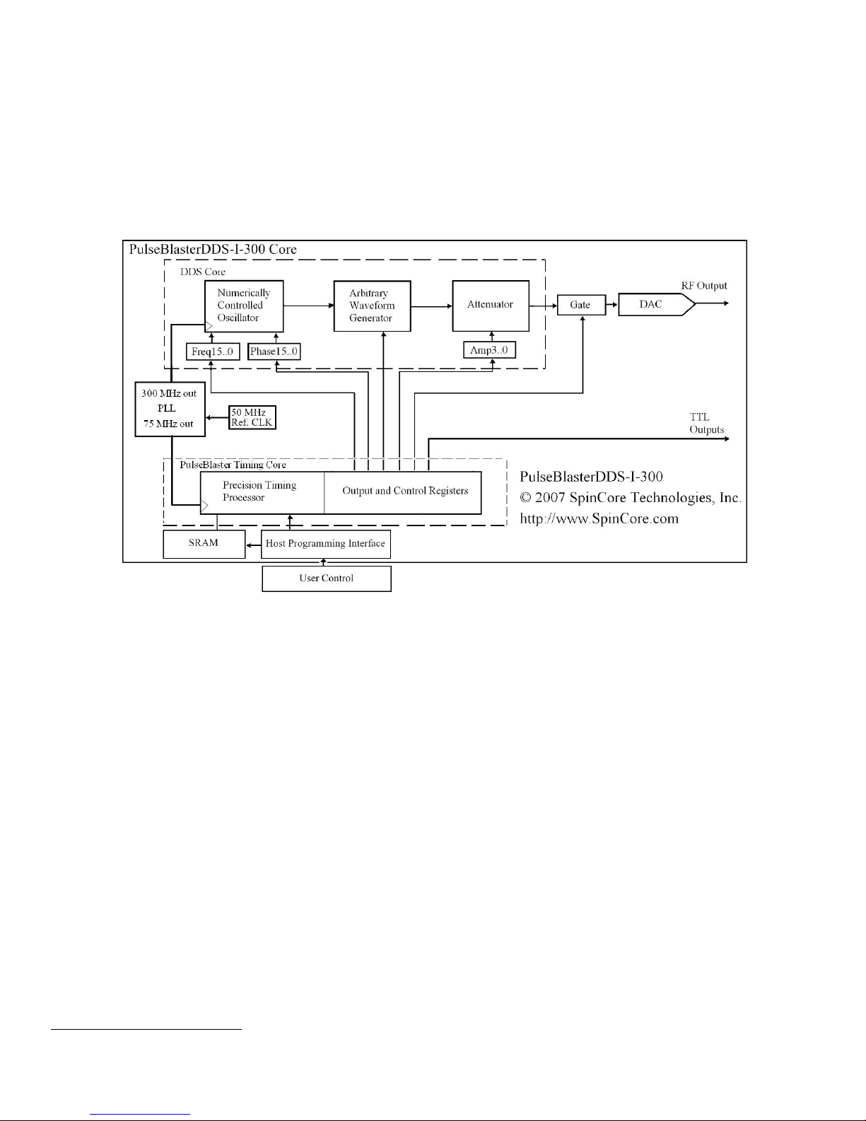
Figure 1, on the next page, presents the general architecture of the PulseBlasterDDS-I-300 board. The two major
building blocks are the DDS Core (top level blocks in Figure 1), and the PulseBlaster Timing Core (PB Core, bottom level
of blocks in Figure 1).
The DDS Core contains a Numerically Controlled Oscillator (NCO) that is equipped with programmable frequency and
phase registers that are under the pulse program control through the PulseBlaster Timing Core. Following the NCO, the
Arbitrary Waveform Generator (AWG) unit can modulate the signal envelope to a user programmable shape, e.g., a sinc
shape. Scaling, or attenuation of the signal amplitude, is also under program control, as well as the additional gating
(blanking) in the digital domain.
http://www.spincore.com 4 2017-11-14
Page 5
PulseBlasterDDS-I-300
The PB Core controls the timing of the gating pulses and provides the necessary control signals for frequency, phase,
shape and amplitude registers. The PB Core also outputs TTL signals to the outside world, as programmed by the user.
The PB processor core executes instructions as written by the user and stored in the on-chip SRAM module, and, once
programmed, the processor operates autonomously.
Figure 1: PulseBlasterDDS-I-300 Board Architecture.
The DDS and PB cores are driven from a common clock source (the 50 MHz1 Reference Clock in Figure 1). The on-
board clock source is removable and, in lieu of the on-board clock, any 3.3 V TTL compatible clock source of arbitrary
stability can be used.
The DDS and PB cores have been integrated onto a single silicon chip. High performance DAC chip and high-current
output amplifier complement the design. User control of the system is provided through the host-programming interface
over the PCI bus or USB controller.
1
A 75 MHz clock may be used with the PulseBlasterDDS-I-300.
http://www.spincore.com 5 2017-11-14
Page 6

PulseBlasterDDS-I-300
Product Specifications
Parameter Min Typ Max Units
Analog Output D/A sampling rate 300 MHz
D/A sampling precision 14 bits
Output voltage range (peak-peak) 1 - 4
(1)
-
V
Phase resolution
Frequency resolution
RF Output
(8)
DC (0 Hz) 100
0.09
1.11
Digital Output Number of digital outputs 4
Logical 1 output voltage 3.3
Logical 0 output voltage
Output drive current 25 mA
Rise/Fall time 1
Digital Input
(HW_Trig,HW_Reset)
Logical 1 input voltage 1.7 4.1 V
Logical 0 input voltage -0.5 0.7 V
Pulse Program # of instruction words 1024 to 4096
Pulse resolution 13.3
Instruction length 66.6 ns 693 days
Table 1: PulseBlasterDDS-I-300 Product Specifications.
(2)
(3)
-
-
deg.
Hz
MHz
(4)
(5)
0
(6)
(7)
9
-
-
-
-
-
V
V
ns
words
ns
Notes
1) Analog output voltage is factor adjustable up to 4 V
for more information.
2) Phase-offset control word is 12-bit wide.
3) Assuming a 50 MHz reference clock and a 300 MHz NCO frequency. Frequency control word is 28-bit wide.
4) On PCI boards, all 24 control bits are routed to on-board IDC header, and signals that are not used internally can
be utilized to control outside devices. Please contact SpinCore if you require more digital outputs; custom
designs with more output bits may be available.
5) This is the value seen without using termination. When the line is terminated with 50 Ω, the output voltage will be
lower.
6) This number can be larger on USB boards. Please contact SpinCore for custom design featuring a larger number
of instruction words.
7) Assuming a 50 MHz reference clock and a 75 MHz PulseBlaster timing core frequency.
8) The RF output can operate from direct current - DC (0 Hz) to 100 MHz. The analog output is DC coupled.
at 10 MHz. See RF Output Level section on the next page
pp
http://www.spincore.com 6 2017-11-14
Page 7
PulseBlasterDDS-I-300
0 20 40 60 80 100 120
0
0.5
1
1.5
2
2.5
3
3.5
4
High Gain
Standard Gain
Frequency (MHz)
Voltage (volts pk-pk on 50 Ohms)
RF Output Level
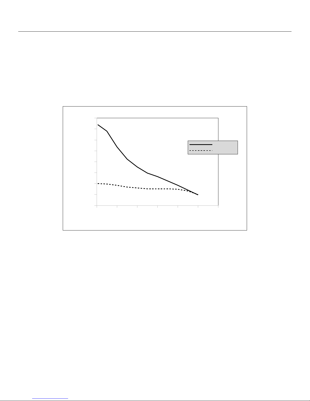
There are currently two different options for PulseBlasterDDS-I-300 RF analog output amplifier – the standard gain and
the high gain. Figure 2, below shows the typical frequency characteristics of the analog output signals for the two output
options. The standard-gain PulseBlasterDDS-I-300 for a 50 Ω load has an output voltage of 1 Volt peak-to-peak at 10
MHz, with a 3 dB bandwidth of about 85 MHz. The high-gain amplifier with a 50 Ω load has a maximum output voltage of
about 3.75 Volts peak-to-peak, with a 3 dB bandwidth of about 21 MHz, while covering the same frequency range as the
standard-gain board.
Figure 2: PulseBlasterDDS-I-300 analog output voltage vs. output frequency. The
dotted line represents the standard-gain output amplifier, and the solid line
represents the high-gain output amplifier. The voltage values are for a 50 Ohm
load impedance. The zero dBm output value for both amplifiers occurs at
approximately 90 MHz.
Please note, the sustained analog output voltage feature is only available on PCI boards. To obtain a sustained
analog output voltage, set the frequency register to 0.0 Hz, and use the content of the phase registers to control the actual
output voltage level.
http://www.spincore.com 7 2017-11-14
Page 8

PulseBlasterDDS-I-300
II. Installation
Installing the PulseBlasterDDS-I-300
To install the board you must complete the following three steps:
1. Download and install the latest SpinAPI software package and example programs on your computer. These are
available at: http://www.spincore.com/support/spinapi/
• SpinAPI is a custom Application Programming Interface (API) package developed by SpinCore Technologies,
Inc. SpinAPI is designed to be used only with SpinCore Technologies, Inc. products. SpinAPI can be utilized
using C/C++, or LabVIEW (described in Section VII).
• SpinAPI contains device drivers and example programs. A shortcut to the location of these files is created
automatically in the Windows Start Menu at “Start>Programs>SpinCore”. See the “readme.txt” file in this
location for more information.
2. Shut down the computer
• For the PCI board: Insert the PulseBlasterDDS-I-300 card into an available PCI slot and fasten the PC
bracket securely with a screw.
• For the USB board: Plug one end of the USB cable into the PulseBlasterDDS-I-300 board and the other
end into the host computer. Next, power the board through the 5-pin DIN-type connector or 6-position
Molex-style connector. We recommend purchasing the RadioProcessorUSB Power Supply, which has the
6-pin output connector and is pin-compatible with the power connector of the PBDDS-I-300-USB board.
For more information on powering the PulseBlasterDDS-I-300 USB board please read Power Connectors
in Section V. USB Connection - Connecting to the PulseBlasterDDS-I-300-USB boards.
• Warning: Do not connect PEG (PCI Express Graphics) power connectors available in some computers
directly to the 6-position Molex-style power connector. Doing so will cause irreparable damage to the
board. SpinCore Technologies is not liable for any damage caused by this.
3. Turn on the computer and follow the installation prompts. Windows may recognize your board as a
RadioProcessor board but the board will still function as it should, as the functionality of the PBDDS-I-300 is a sub-
set of the functionality of the RadioProcessor.
http://www.spincore.com 8 2017-11-14
Page 9
PulseBlasterDDS-I-300
Testing the PulseBlasterDDS-I-300
Once your board is installed properly, the functionality of the device can be tested using three example programs
available from the SpinCore website. All output sequences generated by test programs can be verified using an
oscilloscope.
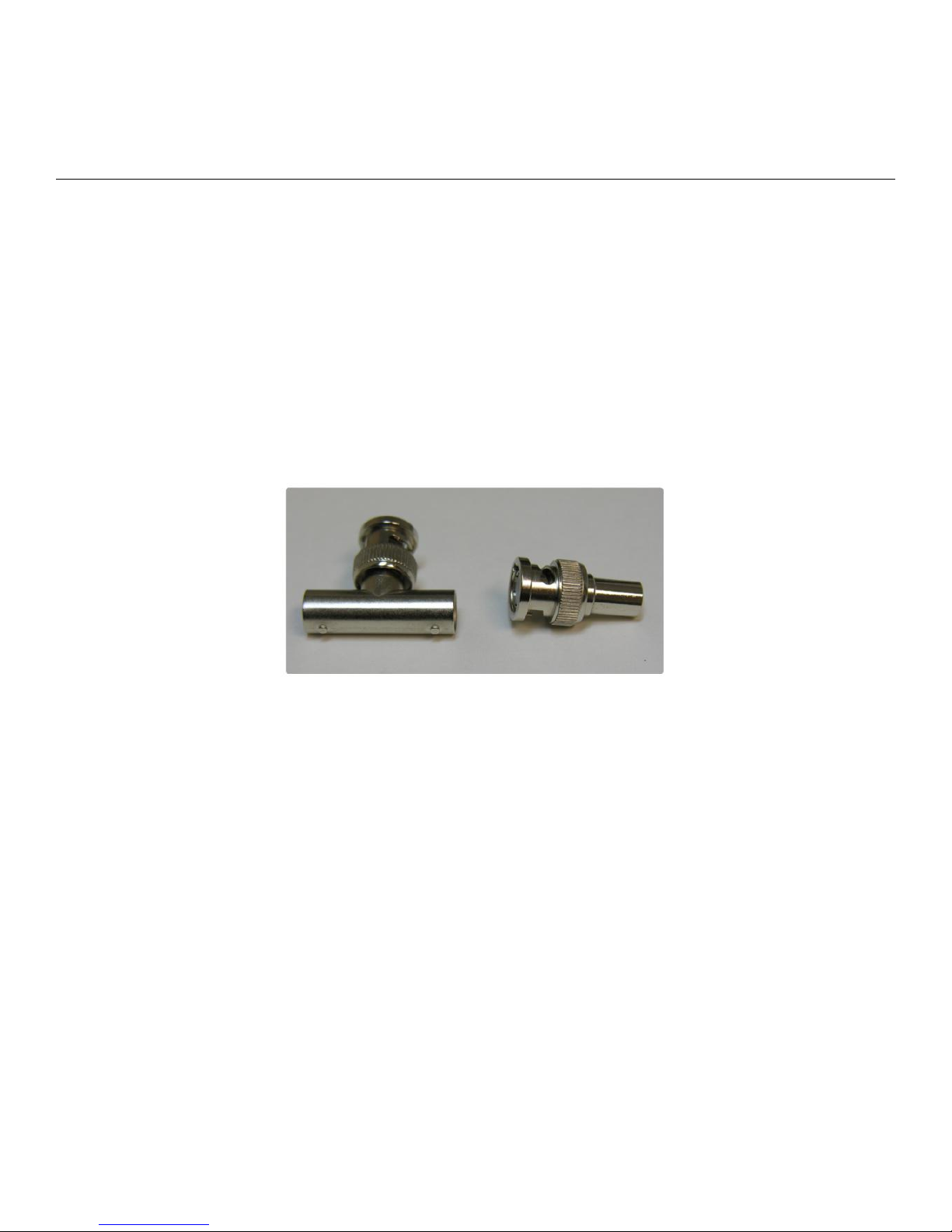
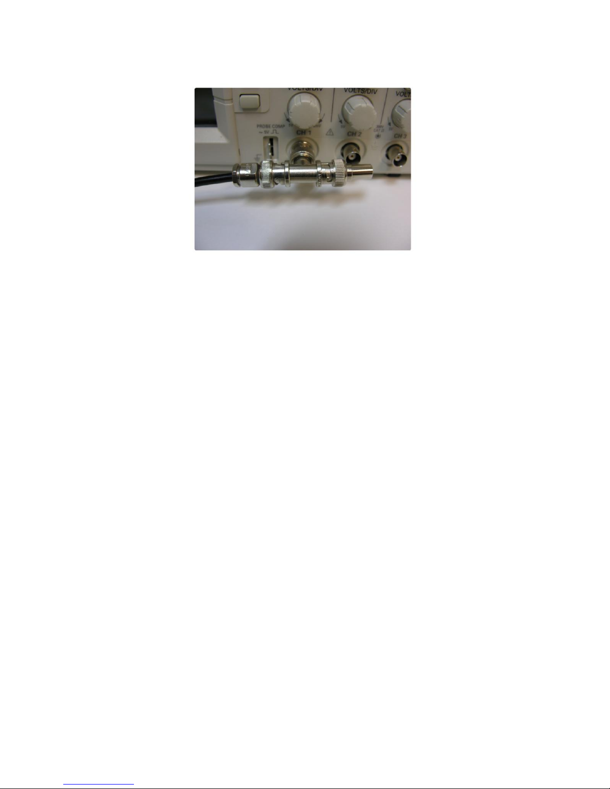
If you are using a high input impedance oscilloscope to monitor the PulseBlasterDDS-I-300's output, place a resistor
that matches the characteristic impedance of the transmission line in parallel with the coaxial transmission line at the
oscilloscope input by attaching it to the line through a T-Adapter(e.g., a 50 Ω resistor with a 50 Ω transmission line, see
Figures 3 and 4 below). For ease of observing the pulsed RF signals, the oscilloscope should be triggered by any of the
TTL outputs. When using an oscilloscope with an adjustable bandwidth, set the bandwidth to as large as possible. Failure
to do so may yield inaccurate readouts on the oscilloscope.
Figure 3: Left: BNC T-Adapter and Right: BNC 50 Ohm
resistor.
http://www.spincore.com 9 2017-11-14
Page 10
PulseBlasterDDS-I-300
Figure 4: BNC T-Adapter on oscilloscope with coaxial
transmission line connected on the left and BNC 50 Ohm
resistor connected on the right, to terminate the line.
The first program is pbdds_i_300_excite_test. This will produce a 1.0 MHz sine wave on the Analog Out connection and
a logical high signal on the Digital Out connection - these signals will turn on for 10 μs and off for 1 ms and will be repeated
indefinitely. The Digital Out on the oscilloscope can be used to trigger the capture of the analog signal.
The signal output can be stopped by using the pb_stop.exe program. The corresponding pb_start.exe will restart the
PBDDS board. Reloading the board with a new program will also stop the execution of any running program.
Next, pbdds_i_300_phase_test will produce a 1.0 MHz output on the Analog Out connection which will turn on for 8 μs
and off for 1 ms. The sin wave will cycle through 4 phase offset registers(one every 2 μs, 90 degrees apart) and will
repeat indefinitely.
To test the AWG feature of the board, use pbdds_i_300_awg. This program will ask for two amplitude values and one
frequency value, and then it will load the board to output two sinc-shaped pulses, one with each amplitude value. This will
repeat every 1 ms.
Along with the executable programs, the folder also contains the C source code of all test programs. Any source code
can be modified, thus allowing the user to start making customized programs as necessary. When SpinAPI tools are
installed on the computer, double-clicking any C source code will launch a graphical integrated environment for easy
editing and rebuilding of new executables via the “Rebuild All” menu functionality.
http://www.spincore.com 10 2017-11-14
Page 11

PulseBlasterDDS-I-300
III. Using the PulseBlasterDDS-I-300
Controlling the PulseBlasterDDS-I-300 with SpinAPI
This section describes the function and use of each feature of the PulseBlasterDDS-I-300.
The PulseBlasterDDS-I-300 is a highly versatile excitation board, and as a result there are many possible approaches
to program the board. However, most applications can be programmed following these basic steps:
1. Load frequency and phase registers with desired values.
2. Load shape and DDS data and amplitude registers (if applicable).
3. Specify a pulse program which will control the timing of the experiment.
4. Trigger the pulse program. The experiment will then proceed autonomously.
These steps are described below. For each of the steps, the relevant SpinAPI functions are listed which control the
actions needed to perform that particular step.
SpinAPI is a control library which allows programs to be written to communicate with your SpinCore board. The most
straightforward way to interface with this library is with a C/C++ program, and the API definitions are described in this
context. However, virtually all programming languages and software environments (including software such as LabView
and Matlab) provide mechanisms for accessing the functionality of standard libraries such as SpinAPI.
Please see the example programs described in the preceding section, “Testing the PulseBlasterDDS-I-300,” for an an
explanation of how to use SpinAPI. A reference document for the API is available online at:
http://spincore.com/support/spinapi/. Under the “Download” bullet there is a link called “API Reference”. An API reference
is also provided in the folder C:\SpinCore\SpinAPI when SpinAPI has been downloaded and installed in the default
location.
Frequency and Phase Registers
The PulseBlasterDDS-I-300 contains one Numerically Controlled Oscillator and associated digital circuitry that drives
the on-board digital-to-analog (DAC) converter, thus forming the Analog Output channel. The frequency and phase of the
output signal are controlled by selecting values from a bank of on-board registers. These registers should be programmed
with appropriate values after board initialization, but before triggering the board. Each pulse instruction selects which
register is used at any given time during an experiment. The number of available registers for each channel is given in the
table below. Certain designs allow the user to select frequency registers using dedicated hardware control lines. See
section VI. External Frequency Modulation for more information.
http://www.spincore.com 11 2017-11-14
Page 12
Relevant SpinAPI functions:
pb_start_programming()
pb_set_phase()
pb_set_freq()
pb_stop_programming()
PulseBlasterDDS-I-300
Register Bank Number of registers
Frequency 16
Phase 16
Table 2: Frequency Register information.
2
3
Sample Output
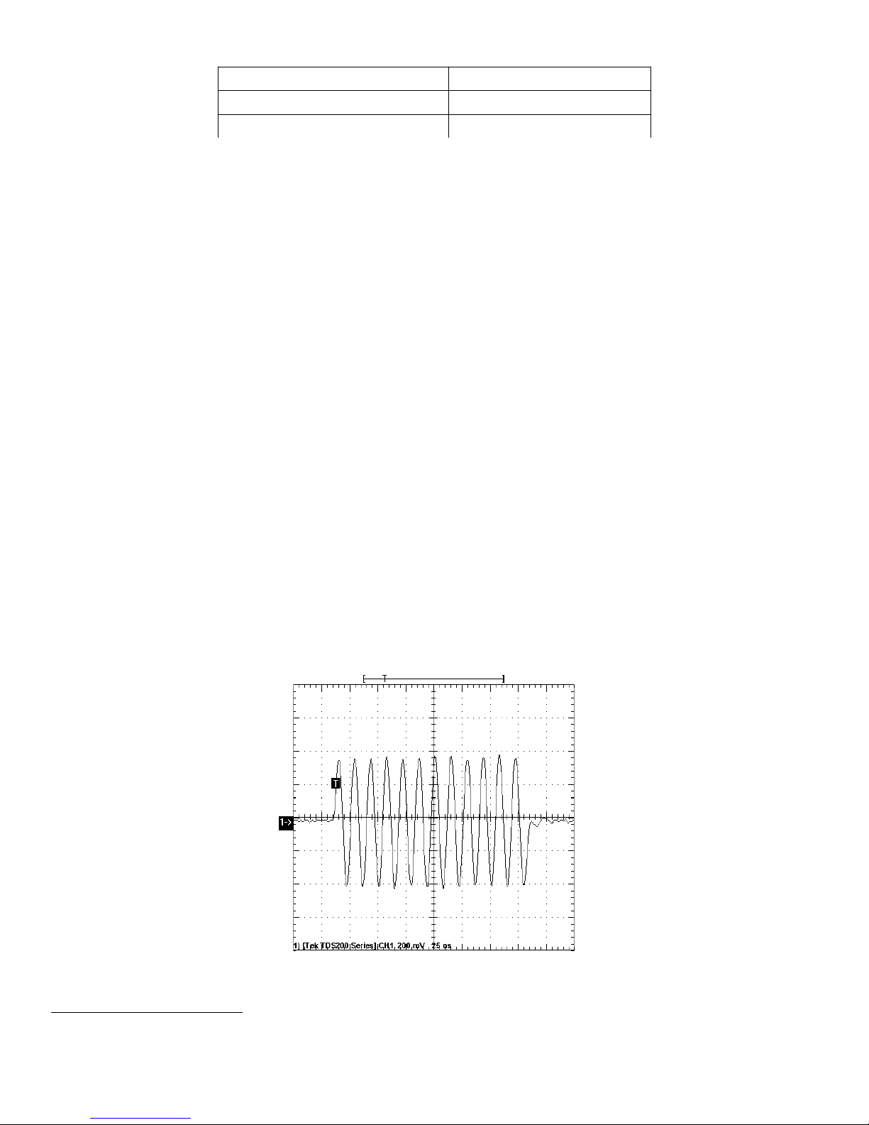
Figure 5, below, shows an example RF 70 MHz output pulse that was generated by the board. The data was captured
using a Tektronix TDS224 oscilloscope. Notice the time base of 25 ns/division.
2
Firmware design 10-16 has been modified to have 1024 frequency registers.
3
Firmware design 10-16 has been modified to have 4 available TX phase registers.
http://www.spincore.com 12 2017-11-14
Figure 5: 185 ns 70 MHz RF/IF output pulse.
Page 13
PulseBlasterDDS-I-300
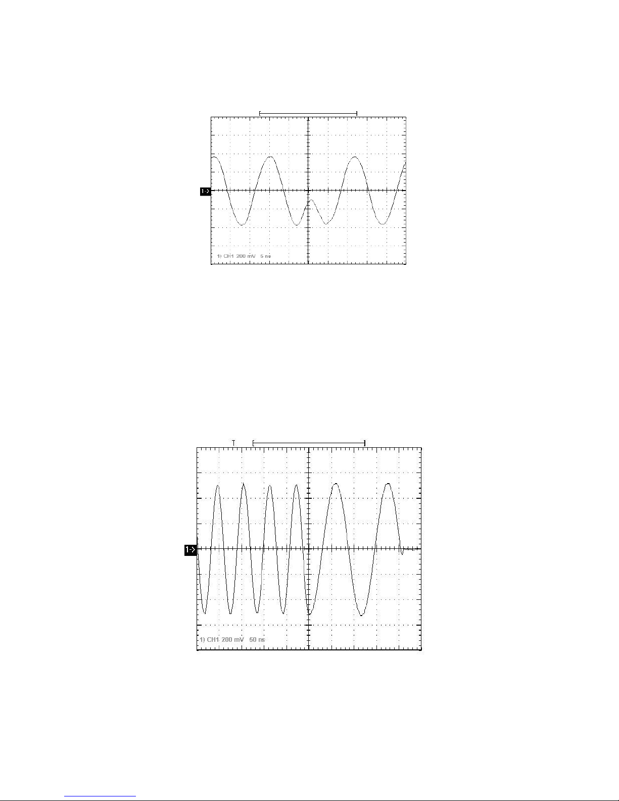
Figure 6, below, demonstrates the zero-latency phase-switching agility. In this figure, two short back-to-back pulses
were recorded with a 180-degree phase offset and a 70 MHz carrier frequency (expanded view).
Figure 6: Two RF output pulses, back to back, with a
180 degree phase switch and 70 MHz RF frequency.
Figure 7, below, demonstrates the frequency-shift agility. In this figure, the frequency jumps from 20 MHz to 10 MHz
with no latency.
Figure 7: Frequency shift from 20 MHz to 10 MHz.
http://www.spincore.com 13 2017-11-14
Page 14

PulseBlasterDDS-I-300
Shape and Amplitude Registers (AWG)
The AWG (Arbitrary Waveform Generator) system can be programmed with a wide variety of parameters. The main
features of this system are:
• RF outputs can be shaped by an arbitrary waveform. (for example, a sinc waveform).
• RF outputs can be scaled by a constant value.
• The RF carrier signal itself can be set to waveforms other than a sinewave (e.g., triangle wave, square wave, etc.).
• The shortest possible pulse is 66.6 ns, the longest is 693 days.
To make use of the AWG feature, use the pb_inst_dds_shape() function to generate the instructions of your pulse
program. This function has two additional parameters over the standard pb_inst_dds() function. They are:
use_shape: if this is 0, no shape will be applied to the pulse. If it is nonzero, whatever waveform is
loaded as the shape will be used to shape the RF pulse. The shape waveform can be loaded by the user
with the pb_dds_load() function
amp: This selects which amplitude register to use. The values stored in the amplitude register can be set with the
pb_set_amp() function.
Relevant SpinAPI functions:
pb_start_programming()
pb_inst_dds()
pb_inst_dds_shape()
pb_stop_programming()
pb_set_amp()
pb_dds_load()
Example program that are included with SpinAPI in the PBDDS-I-300 directory demonstrate how the AWG capabilities
are used. The source code for those programs is well documented, aiding in gaining a better understanding on how the
AWG features of the board are controlled.
Sample Output
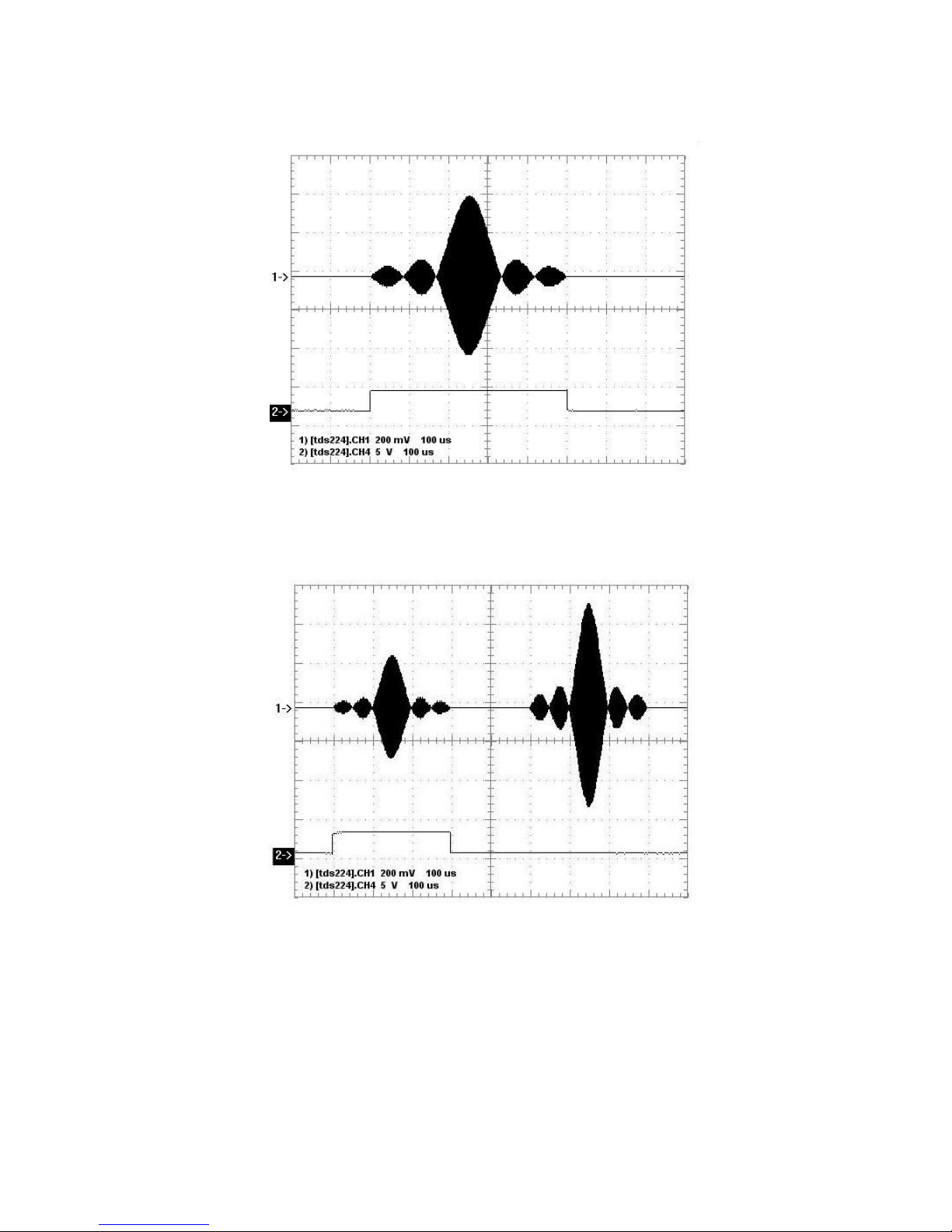
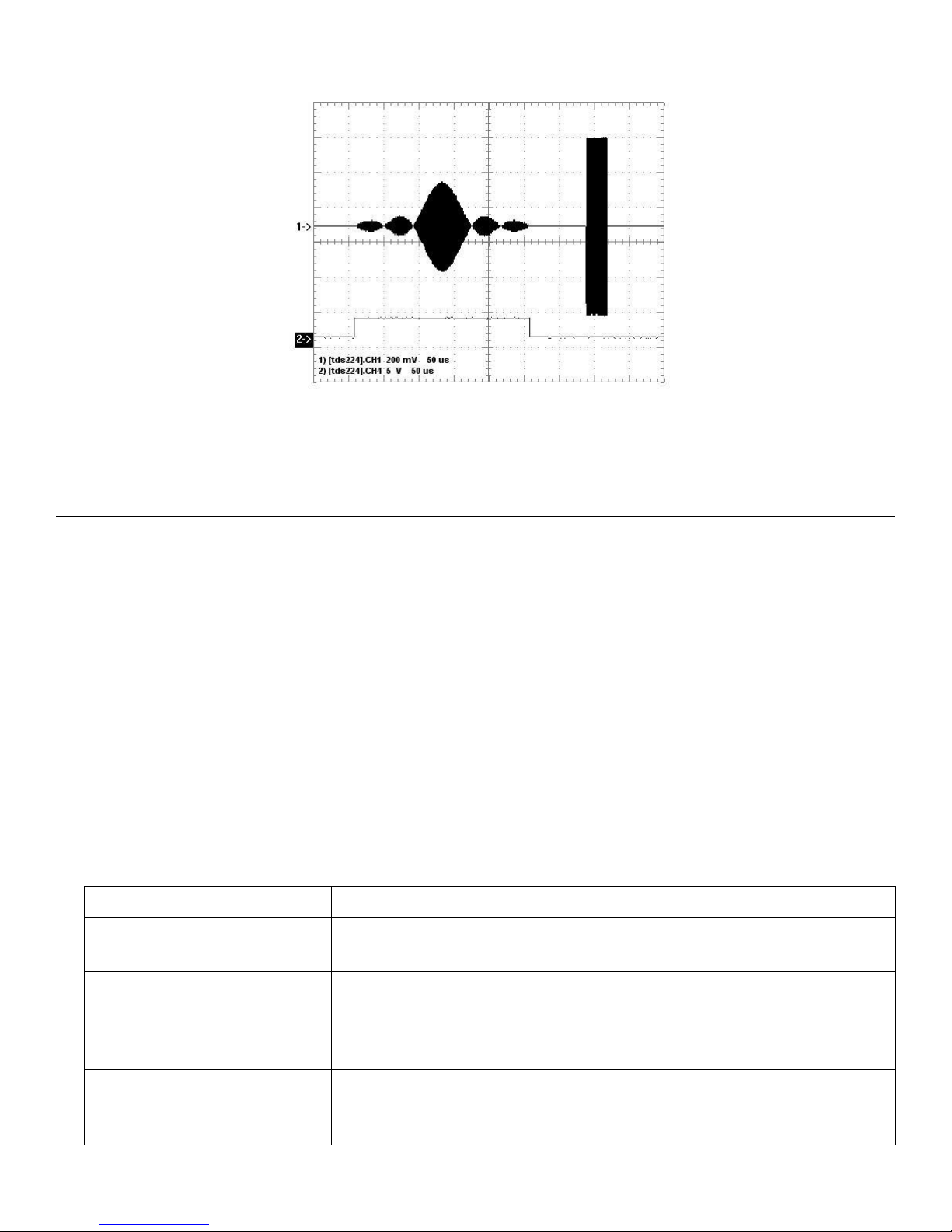
Figures 8-10 illustrate sample capabilities of the AWG features of the PBDDS-I-300 board. Figure 8 demonstrates a
simple sinc-shaped soft pulse of 0.5 ms in duration. The shape of the pulse is not limited to a sinc-shape - it is user-
loadable with any arbitrary waveform. Figure 9 illustrates that multiple soft pulses can be generated in a pulse sequence,
and multiple amplitudes can be assigned to individual pulses. Figure 10 shows that it is also possible to combine soft and
hard RF pulses in a sequence.
http://www.spincore.com 14 2017-11-14
Page 15
PulseBlasterDDS-I-300
Figure 8: Sinc-shaped soft pulse. Pulse duration of 0.5 ms.
Figure 9: Combination of soft RF pulses with variable
http://www.spincore.com 15 2017-11-14
amplitudes.
Page 16
PulseBlasterDDS-I-300
Figure 10: Combination of soft and hard RF pulses in
sequence.
Pulse Programs
The PulseBlasterDDS-I-300 contains an integrated PulseBlaster pulse generation timing core. This timing core
controls all aspects of the systems functionality by setting internal control lines at user specified times. Nine user
programmable digital outputs are also available for control of external hardware. The internal control lines and user
programmable outputs are collectively referred to as flags. The pulse program modifies these flags in a user-defined way
to control all aspects of an experiment.
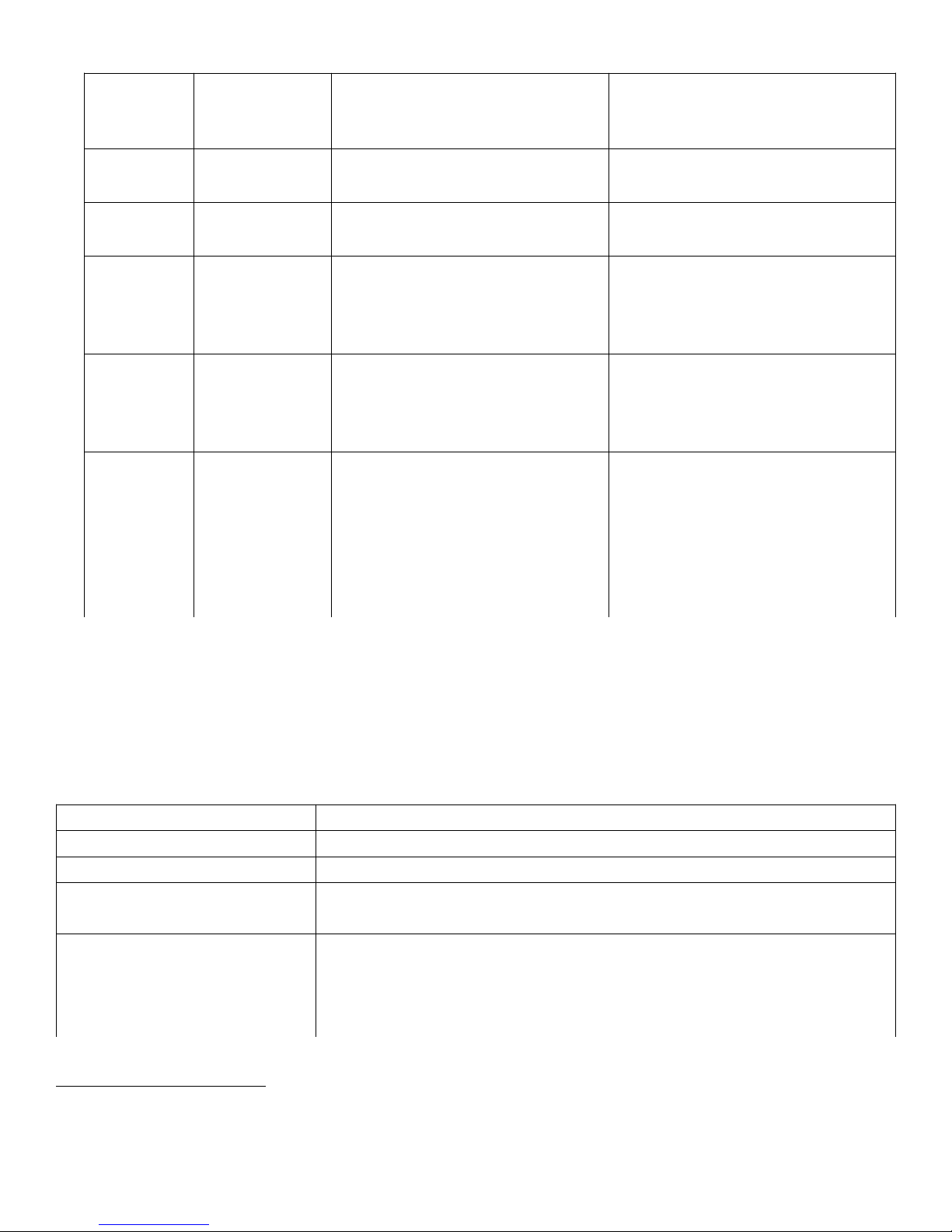
The PulseBlaster uses a robust instruction set to enable the creation of complex pulse programs with ease. Each
instruction is defined by an Operational Code (OpCode) which specifies the action of that instruction and an optional
Instruction data (inst_data) field which elaborates on that action. In addition, each instruction specifies the desired value
for the flags, as well as the execution time of the given instruction, i.e., the delay until the next instruction starts executing.
The “next” instruction is not necessarily the next sequential instruction, as the instruction set contains branching and
looping instructions which can cause the program to be executed out of sequential order. A list of the available instructions
is given in the following table (Table 3).
OpCode # Instruction Inst_data field Function
0 CONTINUE Unused
Program execution continues to next
instruction.
1 STOP Unused
2 LOOP
http://www.spincore.com 16 2017-11-14
Number of desired loops. This
value must be greater than or equal to
1.
Stop execution of program. Analog
outputs turn off. Digital outputs may be
turned off or remain from their previous
state depending on the firmware.
Specify beginning of a loop.
Execution continues to next instruction.
Data used to specify number of loops
Page 17
3 END_LOOP Address of beginning of loop
PulseBlasterDDS-I-300
Specify end of a loop. Execution
returns to begging of loop and
decrements loop counter.
4 JSR
Address of first subroutine
instruction
5 RTS Unused
6 BRANCH Address of instruction to skip to
Number of desired loops. This
7 LONG_DELAY
value must be greater than or equal to
2.
8 WAIT Unused
Program execution jumps to
beginning of a subroutine
Program execution returns to
instruction after JSR was called
Program execution continues at
specified instruction. This behaves like
the goto statement found in many
programming languages
For long interval instructions.
Executes length of pulse given in the
time field multiplied by the value in the
data field.
Program execution pauses and waits
for a software or hardware trigger to
resume it. The latency between a trigger
occurring and the program resuming is
the time used as the delay for the wait
instruction plus a fixed time of 6 clock
cycles.
Table 3: PulseBlaster Instructions.
Control lines
To control the operation of the PulseBlasterDDS-I-300, each instruction in the pulse program specifies a flag word
which sets both the internal control lines and user programmable digital outputs. The control lines stay in the given state
for the duration of the instruction. The internal control lines are described below in Table 4.
Control Line Function
frequency select Selects between the 16 available frequency registers
TX5 channel phase select Selects between the 16 available phase registers
tx_enable Enables TX output on the Analog Out connector. If this control line is disabled,
the Analog Out channel is turned off (zero output voltage).
phase_reset When this control line is enabled, all DDS channels will be reset to their time=0
phase. For example, if a channel is set to use a phase register with 90deg, it will be
reset to the midpoint output level and stay that way until the phase reset control line
is disabled. This allows the the phase of pulses to be synchronized between scans.
Table 4: Internal control lines.
4
6
4
Firmware design 10-16 has been modified to have 1024 available frequency registers.
5
TX refers to RF output.
6
Firmware design 10-16 has been modified to have 4 available phase registers.
http://www.spincore.com 17 2017-11-14
Page 18

PulseBlasterDDS-I-300
Triggering
The PulseBlasterDDS-I-300 can be triggered in two ways, either by software trigger or hardware trigger. The software
trigger is initiated by sending a command from the host PC. Because these boards are typically used with non real-time
operating systems, the exact time between issuing a software trigger and the board acting on that trigger cannot be
precisely specified. For precision control, the pulse program can also be triggered by setting the HW_Trigger pin to a
logical 0. This will cause the pulse program to be triggered within two clock cycles (starting a program), or a minimum of 8
clock cycles (resuming from WAIT instruction).
Triggering the pulse program has one of the following three effects:
1. Begin execution of a pulse program.
2. Restart execution of a pulse program after the board has been reset.
3. Resume execution of a pulse program which is currently paused by a WAIT instruction.
Relevant SpinAPI functions:
pb_start()
Clock output on BNC0
PulseBlasterDDS-I-300 boards have the capability of outputting a 10 MHz7 signal on the BNC0 connector (PCI boards),
or on one of the on-board IDC headers (USB boards). This signal is a 50% duty cycle square wave derived directly from
the on-board 50 MHz clock oscillator, and is intended for synchronization purposes.
To enable this output, call the following SpinAPI function:
pb_set_radio_control(BNC0_CLK);
To have BNC0 return to normal pulse program behavior, call:
pb_unset_radio_control(BNC0_CLK);
If this clock output is enabled, loading the board with another pulse program will not affect the output clock signal. The
10 MHz signal will continue to be present on the output connector until one of the following events occurs: (1) the computer
is turned off, (2) pb_unset_radio_control(BNC0_CLK) is called, or (3) pb_set_defaults() is called. Condition 3
may occur if you are using multiple programs to control your PulseBlasterDDS-I-300, and can be avoided by making sure
that only one of the programs calls pb_set_defaults() and that this program is not run after the one that calls
pb_set_radio_control(BNC0_CLK).
NOTE: When enabled, this option does not affect the functionality of the Digital Output 0 pin on the IDC connector. This
pin will still serve as a digital output under control of the pulse program.
7
Assuming a 50 MHz clock. A 75 MHz clock would give a 15 MHz reference signal.
http://www.spincore.com 18 2017-11-14
Page 19

PulseBlasterDDS-I-300
Clock Input Signal Standard
The PulseBlasterDDS-I-300 is a digital system built in CMOS technology and powered off a 3.3 V DC source. It will
accept external clock signals that conform to the low-voltage 3.3 V TTL standard only. Negative voltage below 0.2 Volts
would damage the processor chip, and thus any external sinusoidal signal would need to be converted to the positive-only
TTL signal prior to using with the PulseBlasterDDS-I-300.
http://www.spincore.com 19 2017-11-14
Page 20
PulseBlasterDDS-I-300
IV. PCI Connection - Connecting to the
PulseBlasterDDS-I-300-PCI boards
Connector Information
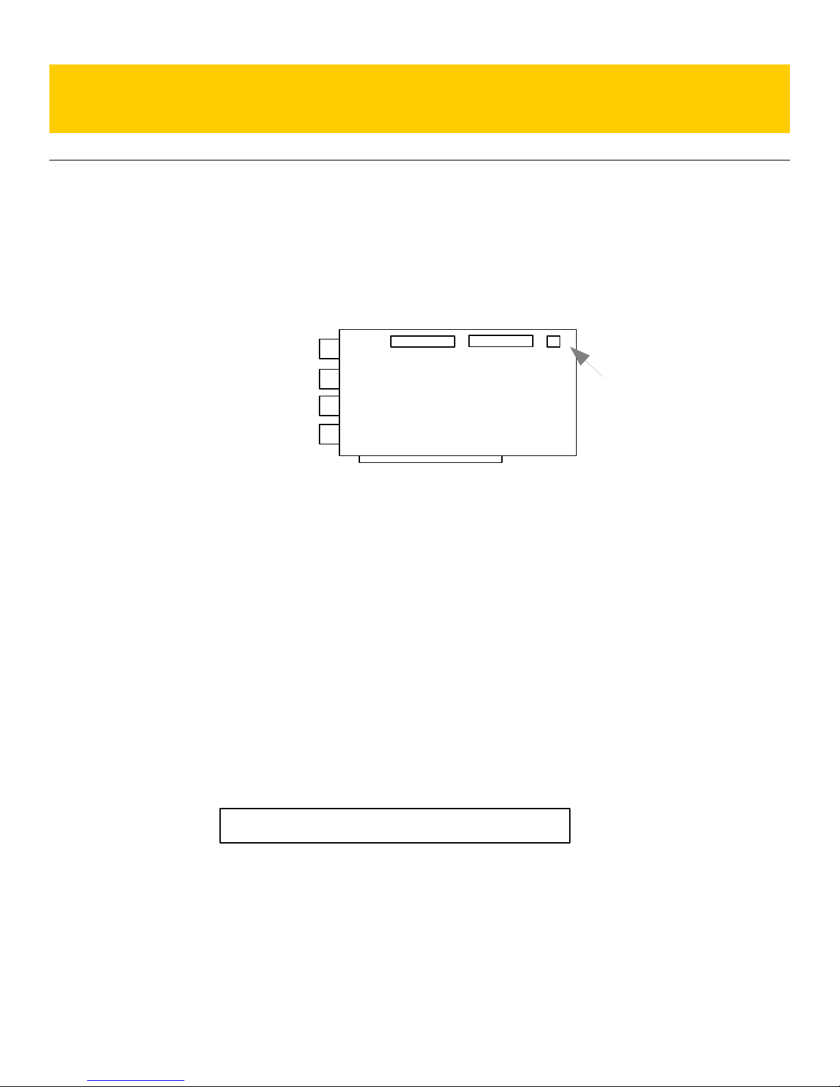
There are two main connector types on the PulseBlasterDDS-I-300 PCI board: the BNC connectors and the IDC
headers – see Figure 11 below. BNC connectors are mounted on the PCI bracket and are available outside of the
computer. The IDC connectors are mounted on-board and are available inside the computer only. There are two long IDC
headers and one short IDC header.
Flag0..11_Out Flag12..23_Out
BNC3 (Not Used)
IDC Headers
BNC2 (Analog Out)
BNC1 (Digital Out)
BNC0 (Digital Out)
IDC Headers
(Digital Out)
Hardware Trigger/Reset
Figure 11: PCI Board Connector Locations.
BNC Connectors
The four BNC connectors provide the primary output interface of the PulseBlasterDDS-I-300 PCI board. All connectors
are impedance matched to 50 Ω. BNC2 is the Analog Output port. BNC1 and BNC0 are both general purpose digital
outputs which can be controlled through the pulse program. BNC3 is not used for the PulseBlasterDDS-I-300.
The analog output connector (BNC2), is not equipped with an interpolating filter. This allows for maximum flexibility in
output frequency, but it means that the output may appear quantized if no filter is used on the output. To eliminate this
behavior and obtain a smooth RF pulse, the user may filter the output with a bandpass or lowpass filter which will cut off
the undesired frequency components above the intended RF signal.
Long IDC Headers
14 15 16 17 18 19 20 21 22 23 24 25 26
1 2 3 4 5 6 7 8 9 10 11 12 13
Figure 12: IDC header pinout.
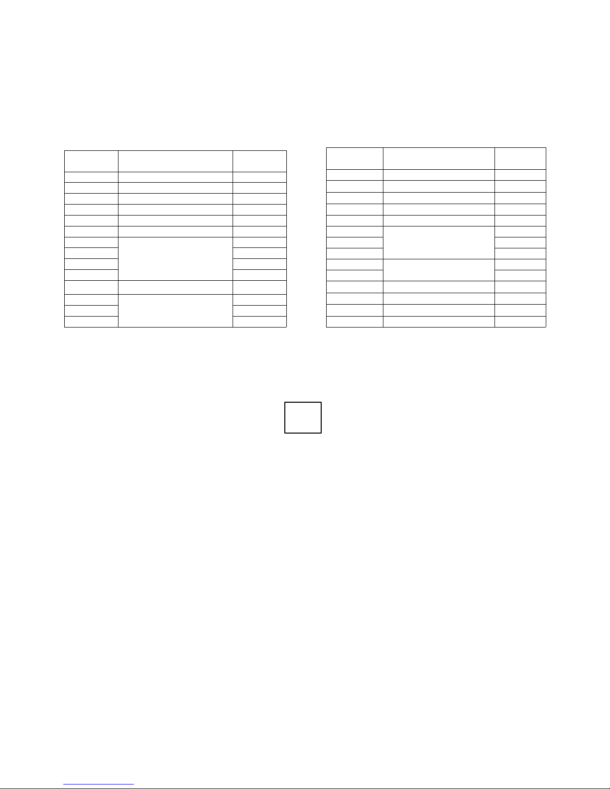
There are two long (2x13 pins) IDC headers on the PulseBlasterDDS-I-300 PCI board. The headers provide access to
all 24 bits of the flag word, nine of which are available to the user as general purpose digital outputs. These are labeled
Flag0..11_Out and Flag12..23_Out. On each IDC header the top row of pins (14-26) are grounds, and the signals are
carried on pins 1-13.
http://www.spincore.com 20 2017-11-14
Page 21
PulseBlasterDDS-I-300
Function
N/A Ground 14-26
N/A Unused 13
23 Digital output 8 12
22 Digital output 7 11
21 Digital output 6 10
20 Digital output 5 9
19
TX phase register select
8
18 7
17 6
16 5
15 tx_enable 4
14
Frequency register select
3
13 2
12 1
Bit in
flag word
Pin on
Flag12..23
Function
N/A Ground 14-26
N/A Unused 13
11 Frequency register select 12
10 Digital output 4 11
9 phase_reset 10
8
Shape period select
9
7 8
6 7
5
Amplitude select
6
4 5
3 Digital output 3 4
2 Digital output 2 3
1 Digital output 1 (BNC1) 2
0 Digital output 0 (BNC0) 1
Bit in flag
word
Pin on
Flag0..11
Each pin on an IDC header corresponds to a bit in the flag field of an instruction. The association between bits and
pins is shown in the table below (Table 5, next page). In the PBDDS-I-300 design, the flag bits that are used to select
frequency and phase registers are also routed to the IDC connectors so external hardware can be used to determine the
state of the program.
HWTrig/Reset Header
Figure 13 presents the layout of the short 2x2 IDC header that is the Hardware Trigger/Reset connector. This is an
input connector, for hardware triggering (HW_Trigger) and resetting (HW_Reset). Pins 3 and 4 are grounds, and pins 1
and 2 are the reset and trigger inputs, respectively. Both inputs are pulled high by an on board 10kΩ pull up resistor.
HW_Trigger (pin 2) When this input detects a falling edge (for example by shorting it with pin 4), a hardware trigger is
produced. This has the same effects as issuing a trigger through software, although the hardware trigger is more precise,
since there are no software latencies involved.
HW_Reset (pin 1) When this input detects a falling edge (for example by shorting it with pin 3), the pulse program is
reset.
http://www.spincore.com 21 2017-11-14
Table 5: IDC connector pin out.
423
Figure 13: HWTrig/Reset
Header pinout.
1
Page 22
PulseBlasterDDS-I-300
V. USB Connection - Connecting to the
PulseBlasterDDS-I-300-USB boards
Power Requirements
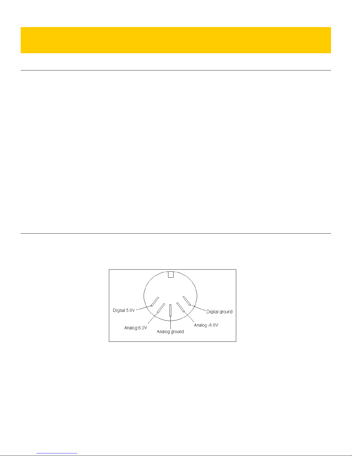
1. Recommended values and maximum currents:
• +5V, 2.0 A (Digital Section)
• +6 V, 1.0 A (Analog Section, Positive Voltage)
• -6 V, 0.2 A (Analog Section, Negative Voltage)
All three voltages need to be applied simultaneously or damage to the board will result.
2. Two independent grounds exist: Digital Ground and Analog Ground. Power sources should be connected as
follows:
• Digital Ground should be connected to the ground point of +5 V supply.
• Analog Ground should be connected to the center point (Ground Point) of the +6V and -6V
supplies.
3. The PulseBlasterDDS-I-300-USB requires USB 2.0 to operate.
Power Connectors
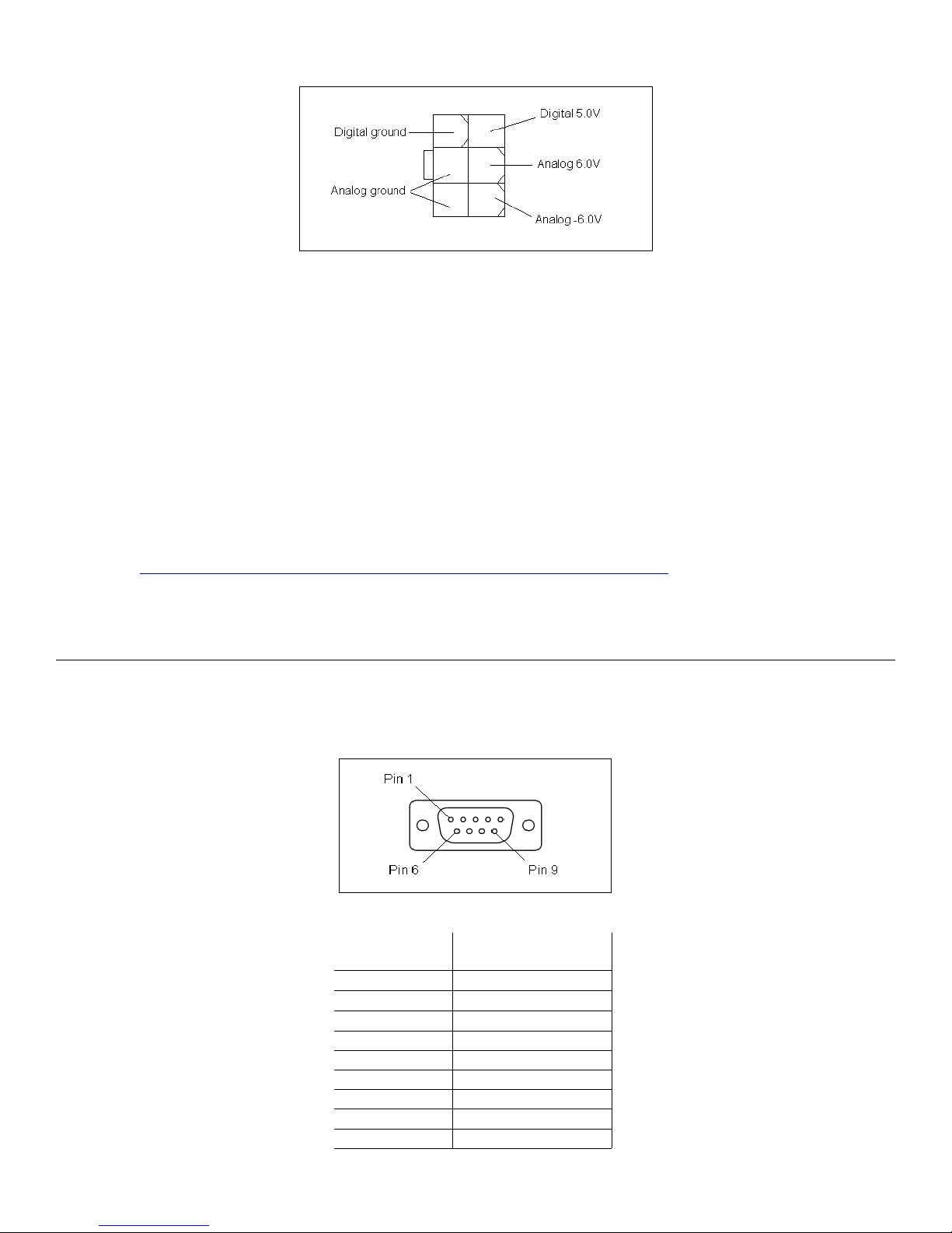
The PBDDS-USB has two power connectors wired in parallel: A 5-pin DIN-type connector and a 6-pin Molex-style
connector. The pin and signal arrangements for these two connection points are shown below in Figures 14 and 15,
respectively.
Figure 14: DIN-5 Power Connector (Power 2).
http://www.spincore.com 22 2017-11-14
Page 23
PulseBlasterDDS-I-300
Pin number Function
1 Flag bit 0
2
Flag bit 1
3 Flag bit 3
4 Flag bit 2
5 Reserved
6 Ground
7
Ground
8 Ground
9 Ground
Figure 15: Molex-style Power Connector (Power 1).
If you will be making your own power supply to connect to the Molex-style power connector, you will need the following
parts or their equivalents: One 6-pin female Mini-Fit Jr.™ connector (DigiKey part No. WM23702-ND) and six Mini-Fit Jr.™
crimp receptacles (DigiKey part No. WM2501-ND).
Warning: Do not connect PEG (PCI Express Graphics) power connectors available in some computers directly to the
6-position Molex-style power connector. Doing so will cause irreparable damage to the board. SpinCore Technologies is
not liable for any damage caused by this.
A dedicated DC/DC power supply is optionally available from SpinCore Technologies, Inc. For more information,
please see: http://spincore.com/products/SP11/RadioProcessor-USB-Power-Supply.shtml or the Related Products and
Accessories section below.
Digital Output Connectors
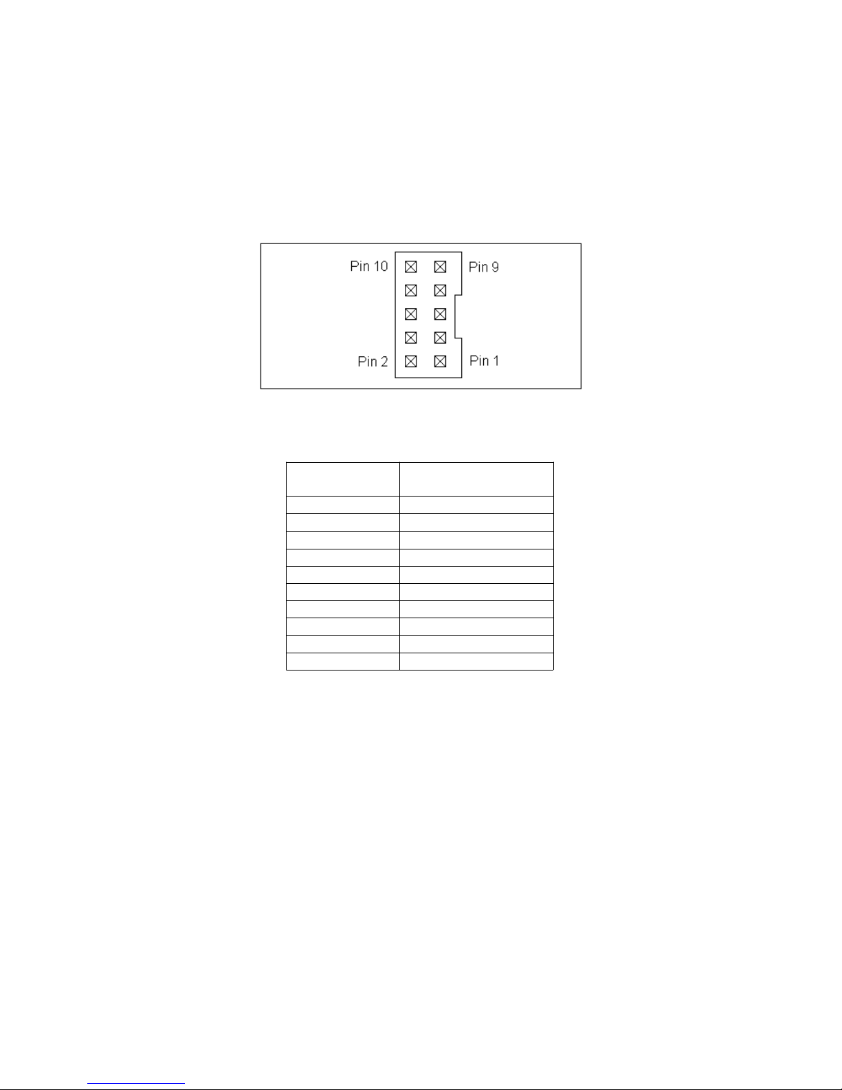
The digital outputs of the PBDDS-USB are present on both the J300 and J301 connectors. J300 is a standard DB-9
connector and J301 is a 5x2 shrouded IDC header. The pinouts of these connectors and the corresponding signal names
are shown on the next page in Figures 16 and 17 and Table 6 and Table 7 respectively.
Figure 16: DB-9 Output Connector J300.
http://www.spincore.com 23 2017-11-14
Page 24
PulseBlasterDDS-I-300
Pin number Function
1 Ground
2
Flag bit 0
3 Ground
4 Flag bit 1
5 Ground
6 Flag bit 3
7
Ground
8 Flag bit 2
9 Ground
10 Reserved
Table 6: DB-9 Output Connector J300 signal list.
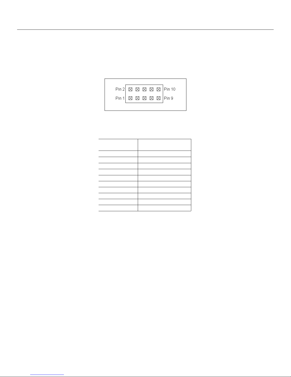
Figure 17: Shrouded IDC Output Header J301.
Table 7: Shrouded IDC Output Header J301 signal list.
http://www.spincore.com 24 2017-11-14
Page 25
PulseBlasterDDS-I-300
Pin number Function
1 Ground
2
10 MHz out or N/C
3 Ground
4 N/C
5 Ground
6 N/C
7
Ground
8 Hardware Trigger
9 Ground
10 Hardware Reset
Header JP302
The unshrouded male header labeled JP302 contains the Hardware Trigger and Hardware Reset lines. This header, see
Figure 18 and Table 8, on the next page, for the layout and pin assignments, also offers a 10 MHz output that is derived
from the master clock oscillator. This signal is ideal for synchronization purposes and is present on pin 2 of the header.
Figure 18: Output Header JP302.
Table 8: Output Header JP302 signal list.
HW_Trigger (pin 8) When this input detects a falling edge (for example by shorting it with pin 4), a hardware trigger is
produced. This has the same effects as issuing a trigger through software, although the hardware trigger is more precise,
since there are no software latencies involved.
HW_Reset (pin 10) When this input detects a falling edge (for example by shorting it with pin 3), the pulse program is
reset.
http://www.spincore.com 25 2017-11-14
Page 26
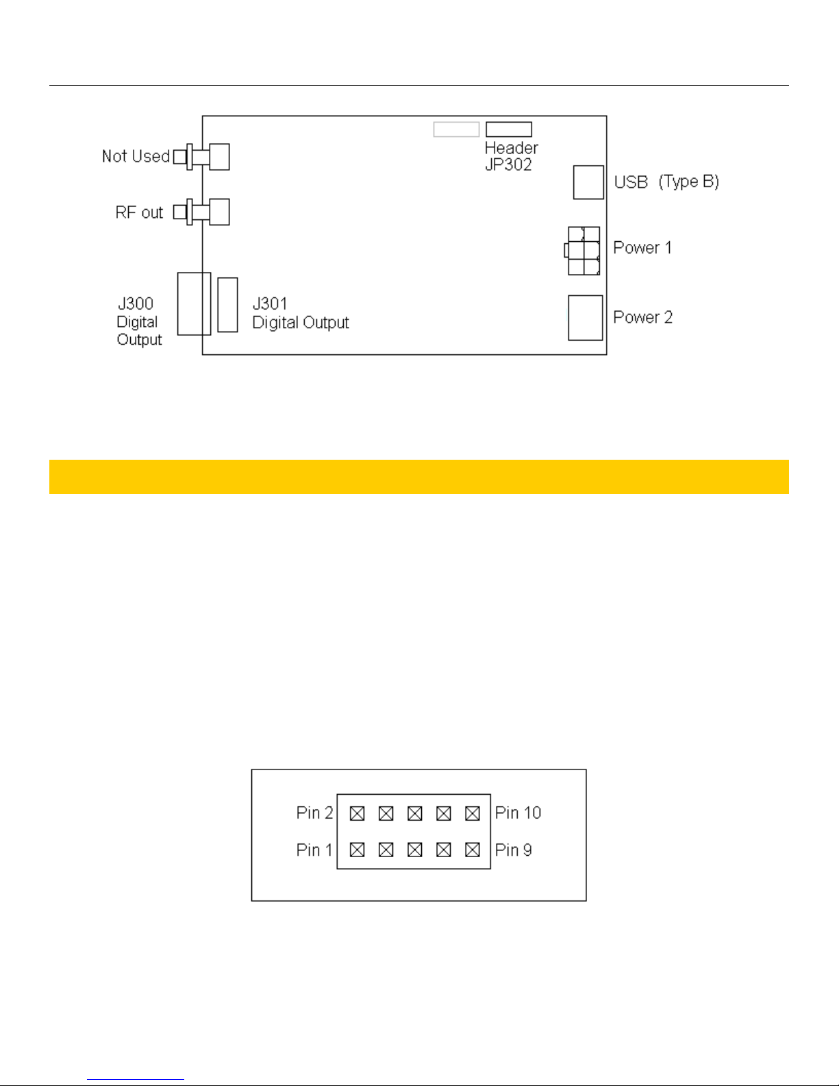
Connector Locations
PulseBlasterDDS-I-300
Figure 19: USB Board Connector Locations.
VI. External Frequency Modulation
There exists a custom firmware design(EEPROM Code 12-12) which allows the user to select between frequency
registers using dedicated hardware control lines to perform FSK modulation. The use of these frequency control lines to
select between frequency registers is described below.
Header JP302 (Frequency Select and HW Trigger/Reset)
The unshrouded male header labeled JP302 contains the three hardware Frequency Select pins in addition to the
Hardware Trigger and Hardware Reset pins.
http://www.spincore.com 26 2017-11-14
Figure 20: Output Header JP302.
Page 27
PulseBlasterDDS-I-300
Pin number Function
1 Ground
2
Frequency Select 0
3 Ground
4 Frequency Select 1
5 Ground
6 Frequency Select 2
7
Ground
8 Hardware Trigger
9 Ground
10 Hardware Reset
Table 9: Output Header JP302 signal list.
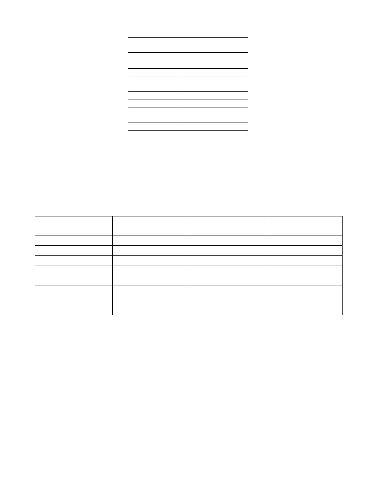
Designs with external frequency modulation control have three hardware frequency select input pins located as shown
in Table 9 above. These three pins can be used to select between eight different frequency registers. To use the hardware
frequency select lines set the software frequency register parameter to zero and drive the hardware frequency select lines
as necessary. Table 10 below shows appropriate values to select between the frequency registers where a '1' refers to a
3.3 V TTL high state and '0' refers to a TTL low state (ground).
HW Frequency Select2HW Frequency Select1HW Frequency Select0Frequency Register
0 0 0
0 0 1
0 1 0
0 1 1
1 0 0
1 0 1
1 1 0
1 1 1
Table 10: Frequency Register Selection list. In order to use the hardware frequency select lines
be sure to set the software frequency register select value to 0.
0
1
2
3
4
5
6
7
Important Notes:
• To select between frequency registers via software, all hardware frequency select lines must first be set to logical
0. Software frequency selection is performed by setting the frequency register select parameter (the first argument of
the pb_inst_radio(...) or pb_inst_radio_shape(...) functions) to the desired value.
• To select between frequency registers via hardware, the software frequency register select parameter must first be
set to 0.
• The hardware frequency select input lines are pulled low by on board five11Ω pull-down resistors. Therefore the
default state when nothing is connected is logical 0.
http://www.spincore.com 27 2017-11-14
Page 28
PulseBlasterDDS-I-300
VII. PulseBlasterDDS-I-300 Interface for LabVIEW
Overview of SpinCore LabVIEW GUI Interface
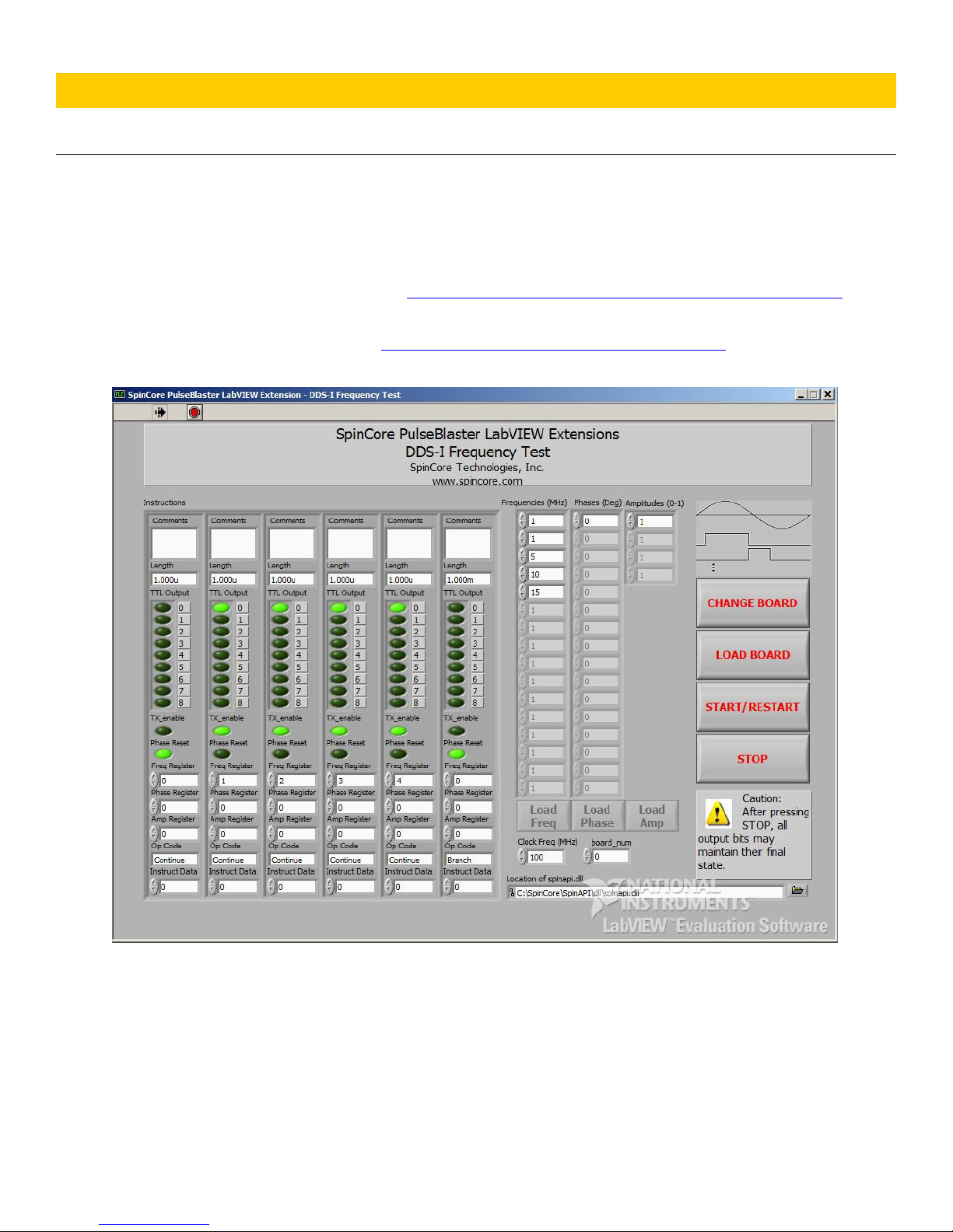
SpinCore has developed an easy-to-use LabVIEW Graphical User Interface (GUI) that allows the user to program
and control PulseBlasterDDS-I-300 boards. Simply set the parameters as described in this manual and run the program to
control the digital pulse and RF generation of the board. A sample screenshot is shown on the next page.
For more information see the LabVIEW manual at: http://www.spincore.com/support/PBLV/PBLV_DDS_Manual.pdf
The LabVIEW interface can be downloaded at: http://www.spincore.com/support/PBLV/DDS.shtml
Figure 21: Example of PulseBlasterDDS-I-300 LabVIEW Extensions User Interface.
http://www.spincore.com 28 2017-11-14
Page 29

PulseBlasterDDS-I-300
Related Products and Accessories
1. PulseBlasterDDS-II-300-AWG – A programmable TTL and Dual Channel Direct Digital Synthesis RF Pulse
Generator. For more information, please visit http://www.spincore.com/products/PulseBlasterDDS-II-300/
2. RadioProcessor - Complete single-card solution for RF pulse generation and acquisition. For more information,
please visit http://www.spincore.com/products/RadioProcessor/
3. If you require a specific number of amplitude registers, memory words, alternative clock frequencies, or an Oven
Controlled Crystal Oscillator (OCXO), please inquire with SpinCore Technologies through our contact form, which
is available at http://www.spincore.com/contact.shtml
4. Power Supply for PulseBlasterDDS-I-300-USB boards. For more information, please visit:
http://www.spincore.com/products/SP11/RadioProcessor-USB-Power-Supply.shtml
Contact Information
SpinCore Technologies, Inc.
4631 NW 53rd Avenue, SUITE 103
Gainesville, FL 32653
USA
Telephone (USA): 352-271-7383
Fax (USA): 352-371-8679
Website: http://www.spincore.com
Web Contact Form: http://spincore.com/contact.shtml
Document Information
For revision history, please contact SpinCore.
http://www.spincore.com 29 2017-11-14
 Loading...