

SpinCore Technologies DDS-I-300, PulseBlasterDDS Owner's Manual
PulseBlasterDDS™
Model DDS-I-300
(USB Board Version SP7)
Owner’s Manual
SpinCore Technologies, Inc.
http://www.spincore.com

PulseBlasterDDS-I-300
Congratulations and thank you for choosing a design from SpinCore
Technologies, Inc.
We appreciate your business!
At SpinCore we try to fully support the needs of our customers. If you are in
need of assistance, please contact us and we will strive to provide the
necessary support.
© 2007 - 2017 SpinCore Technologies, Inc. All rights reserved.
SpinCore Technologies, Inc. reserves the right to make changes to the product(s) or information herein without notice.
PulseBlasterDDS™, PulseBlaster™, SpinCore, and the SpinCore Technologies, Inc. logos are trademarks of SpinCore Technologies, Inc. All other
trademarks are the property of their respective owners.
SpinCore Technologies, Inc. makes every effort to verify the correct operation of the equipment. This equipment version is not intended for use in a
system in which the failure of a SpinCore device will threaten the safety of equipment or person(s).
http://www.spincore.com 2 2017-11-14

PulseBlasterDDS-I-300
Table of Contents
Table of Contents ................................................................................................................................... 3
I. Introduction ......................................................................................................................................... 4
Product Overview ....................................................................................................................................................... 4
Board Architecture ...................................................................................................................................................... 4
Block Diagram ....................................................................................................................................................... 4
Product Specifications ................................................................................................................................................ 6
RF Output Level ........................................................................................................................................................... 7
II. Installation .......................................................................................................................................... 8
Installing the PulseBlasterDDS-I-300 ......................................................................................................................... 8
Testing the PulseBlasterDDS-I-300 ............................................................................................................................. 9
III. Using the PulseBlasterDDS-I-300 ................................................................................................. 11
Controlling the PulseBlasterDDS-I-300 with SpinAPI .............................................................................................. 11
Frequency and Phase Registers ............................................................................................................................... 11
Sample Output ..................................................................................................................................................... 12
Shape and Amplitude Registers (AWG) ................................................................................................................... 14
Sample Output ..................................................................................................................................................... 14
Pulse Programs .......................................................................................................................................................... 16
Control lines ......................................................................................................................................................... 17
Triggering ................................................................................................................................................................... 18
Clock output on BNC0 ............................................................................................................................................... 18
Clock Input Signal Standard ..................................................................................................................................... 19
IV. PCI Connection - Connecting to the PulseBlasterDDS-I-300-PCI boards ................................ 20
Connector Information .............................................................................................................................................. 20
BNC Connectors .................................................................................................................................................. 20
Long IDC Headers ............................................................................................................................................... 20
HWTrig/Reset Header .......................................................................................................................................... 21
V. USB Connection - Connecting to the PulseBlasterDDS-I-300-USB boards .............................. 22
Power Requirements ................................................................................................................................................. 22
Power Connectors .................................................................................................................................................... 22
Digital Output Connectors ....................................................................................................................................... 23
Header JP302 ............................................................................................................................................................ 25
Connector Locations ................................................................................................................................................. 25
VI. External Frequency Modulation .................................................................................................. 26
Header JP302 (Frequency Select and HW Trigger/Reset) ................................................................................... 26
Important Notes: .................................................................................................................................................. 27
VII. PulseBlasterDDS-I-300 Interface for LabVIEW .......................................................................... 27
Overview of SpinCore LabVIEW GUI Interface ........................................................................................................ 27
Related Products and Accessories ................................................................................................... 28
Contact Information ............................................................................................................................. 29
Document Information ........................................................................................................................ 29
http://www.spincore.com 3 2017-11-14

PulseBlasterDDS-I-300
I. Introduction
Product Overview
PulseBlasterDDS is a high-performance signal generator that combines two units – the digital waveform synthesis unit
(DDS, Direct Digital Synthesis), and the PulseBlaster Timing Processor.
The PulseBlaster Timing Processor provides all the necessary timing control signals required for overall system control
and pulse synchronization. This part of the PulseBlasterDDS design also generates the programmable-length digital (TTL
logic) pulses. By adding DDS features, PulseBlasterDDS can now provide not only programmable TTL pulses but also
RF (Radio Frequency) output signals. By utilizing the PulseBlaster Timing Processor core, the combined system can
generate sophisticated pulse sequences with single-clock accuracy, meeting high-performance demands of advanced
users.
The PulseBlasterDDS-I-300 is equipped with one 300 MHz DAC (Digital-to-Analog Converter), and it can produce
useful output signal frequencies from DC (Direct Current) (0 Hz) to 100 MHz. Arbitrary Waveform Generation (AWG),
output gating and attenuation, and user-programmable amplitude, frequency, and phase modulation are standard. In
addition to the ability to modulate the envelope of the generated signal, the shape of the carrier signal can be custom-
defined as well, giving the user the opportunity to explore novel excitation modes. Select designs allow for external
frequency modulation using dedicated hardware input lines.
Packaged in a small USB form factor, the PulseBlasterDDS-I-300 series of boards provide users the ability to control
their systems through the generation of fully synchronized digital and analog excitation pulses, ranging from simple RF and
TTL pulses to sophisticated excitation schemes with nested loops, subroutines, etc., providing users with a compelling
price/performance proposition unmatched by any other device on the market today.
Please note that currently, the PCI board version SP6 is only available for special orders.
Board Architecture
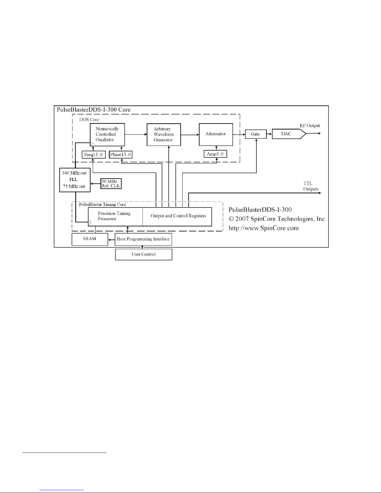
Block Diagram
Figure 1, on the next page, presents the general architecture of the PulseBlasterDDS-I-300 board. The two major
building blocks are the DDS Core (top level blocks in Figure 1), and the PulseBlaster Timing Core (PB Core, bottom level
of blocks in Figure 1).
The DDS Core contains a Numerically Controlled Oscillator (NCO) that is equipped with programmable frequency and
phase registers that are under the pulse program control through the PulseBlaster Timing Core. Following the NCO, the
Arbitrary Waveform Generator (AWG) unit can modulate the signal envelope to a user programmable shape, e.g., a sinc
shape. Scaling, or attenuation of the signal amplitude, is also under program control, as well as the additional gating
(blanking) in the digital domain.
http://www.spincore.com 4 2017-11-14
PulseBlasterDDS-I-300
The PB Core controls the timing of the gating pulses and provides the necessary control signals for frequency, phase,
shape and amplitude registers. The PB Core also outputs TTL signals to the outside world, as programmed by the user.
The PB processor core executes instructions as written by the user and stored in the on-chip SRAM module, and, once
programmed, the processor operates autonomously.
Figure 1: PulseBlasterDDS-I-300 Board Architecture.
The DDS and PB cores are driven from a common clock source (the 50 MHz1 Reference Clock in Figure 1). The on-
board clock source is removable and, in lieu of the on-board clock, any 3.3 V TTL compatible clock source of arbitrary
stability can be used.
The DDS and PB cores have been integrated onto a single silicon chip. High performance DAC chip and high-current
output amplifier complement the design. User control of the system is provided through the host-programming interface
over the PCI bus or USB controller.
1
A 75 MHz clock may be used with the PulseBlasterDDS-I-300.
http://www.spincore.com 5 2017-11-14

PulseBlasterDDS-I-300
Product Specifications
Parameter Min Typ Max Units
Analog Output D/A sampling rate 300 MHz
D/A sampling precision 14 bits
Output voltage range (peak-peak) 1 - 4
(1)
-
V
Phase resolution
Frequency resolution
RF Output
(8)
DC (0 Hz) 100
0.09
1.11
Digital Output Number of digital outputs 4
Logical 1 output voltage 3.3
Logical 0 output voltage
Output drive current 25 mA
Rise/Fall time 1
Digital Input
(HW_Trig,HW_Reset)
Logical 1 input voltage 1.7 4.1 V
Logical 0 input voltage -0.5 0.7 V
Pulse Program # of instruction words 1024 to 4096
Pulse resolution 13.3
Instruction length 66.6 ns 693 days
Table 1: PulseBlasterDDS-I-300 Product Specifications.
(2)
(3)
-
-
deg.
Hz
MHz
(4)
(5)
0
(6)
(7)
9
-
-
-
-
-
V
V
ns
words
ns
Notes
1) Analog output voltage is factor adjustable up to 4 V
for more information.
2) Phase-offset control word is 12-bit wide.
3) Assuming a 50 MHz reference clock and a 300 MHz NCO frequency. Frequency control word is 28-bit wide.
4) On PCI boards, all 24 control bits are routed to on-board IDC header, and signals that are not used internally can
be utilized to control outside devices. Please contact SpinCore if you require more digital outputs; custom
designs with more output bits may be available.
5) This is the value seen without using termination. When the line is terminated with 50 Ω, the output voltage will be
lower.
6) This number can be larger on USB boards. Please contact SpinCore for custom design featuring a larger number
of instruction words.
7) Assuming a 50 MHz reference clock and a 75 MHz PulseBlaster timing core frequency.
8) The RF output can operate from direct current - DC (0 Hz) to 100 MHz. The analog output is DC coupled.
at 10 MHz. See RF Output Level section on the next page
pp
http://www.spincore.com 6 2017-11-14
PulseBlasterDDS-I-300
0 20 40 60 80 100 120
0
0.5
1
1.5
2
2.5
3
3.5
4
High Gain
Standard Gain
Frequency (MHz)
Voltage (volts pk-pk on 50 Ohms)
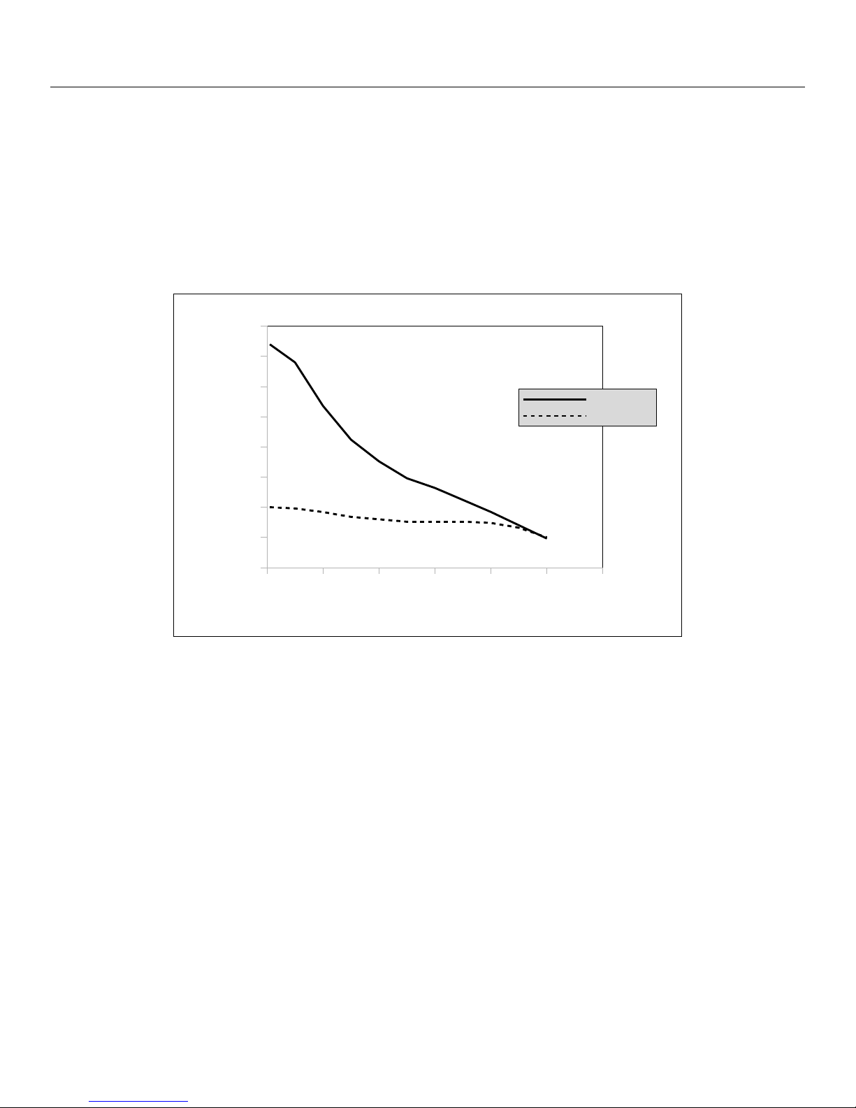
RF Output Level
There are currently two different options for PulseBlasterDDS-I-300 RF analog output amplifier – the standard gain and
the high gain. Figure 2, below shows the typical frequency characteristics of the analog output signals for the two output
options. The standard-gain PulseBlasterDDS-I-300 for a 50 Ω load has an output voltage of 1 Volt peak-to-peak at 10
MHz, with a 3 dB bandwidth of about 85 MHz. The high-gain amplifier with a 50 Ω load has a maximum output voltage of
about 3.75 Volts peak-to-peak, with a 3 dB bandwidth of about 21 MHz, while covering the same frequency range as the
standard-gain board.
Figure 2: PulseBlasterDDS-I-300 analog output voltage vs. output frequency. The
dotted line represents the standard-gain output amplifier, and the solid line
represents the high-gain output amplifier. The voltage values are for a 50 Ohm
load impedance. The zero dBm output value for both amplifiers occurs at
approximately 90 MHz.
Please note, the sustained analog output voltage feature is only available on PCI boards. To obtain a sustained
analog output voltage, set the frequency register to 0.0 Hz, and use the content of the phase registers to control the actual
output voltage level.
http://www.spincore.com 7 2017-11-14

PulseBlasterDDS-I-300
II. Installation
Installing the PulseBlasterDDS-I-300
To install the board you must complete the following three steps:
1. Download and install the latest SpinAPI software package and example programs on your computer. These are
available at: http://www.spincore.com/support/spinapi/
• SpinAPI is a custom Application Programming Interface (API) package developed by SpinCore Technologies,
Inc. SpinAPI is designed to be used only with SpinCore Technologies, Inc. products. SpinAPI can be utilized
using C/C++, or LabVIEW (described in Section VII).
• SpinAPI contains device drivers and example programs. A shortcut to the location of these files is created
automatically in the Windows Start Menu at “Start>Programs>SpinCore”. See the “readme.txt” file in this
location for more information.
2. Shut down the computer
• For the PCI board: Insert the PulseBlasterDDS-I-300 card into an available PCI slot and fasten the PC
bracket securely with a screw.
• For the USB board: Plug one end of the USB cable into the PulseBlasterDDS-I-300 board and the other
end into the host computer. Next, power the board through the 5-pin DIN-type connector or 6-position
Molex-style connector. We recommend purchasing the RadioProcessorUSB Power Supply, which has the
6-pin output connector and is pin-compatible with the power connector of the PBDDS-I-300-USB board.
For more information on powering the PulseBlasterDDS-I-300 USB board please read Power Connectors
in Section V. USB Connection - Connecting to the PulseBlasterDDS-I-300-USB boards.
• Warning: Do not connect PEG (PCI Express Graphics) power connectors available in some computers
directly to the 6-position Molex-style power connector. Doing so will cause irreparable damage to the
board. SpinCore Technologies is not liable for any damage caused by this.
3. Turn on the computer and follow the installation prompts. Windows may recognize your board as a
RadioProcessor board but the board will still function as it should, as the functionality of the PBDDS-I-300 is a sub-
set of the functionality of the RadioProcessor.
http://www.spincore.com 8 2017-11-14
PulseBlasterDDS-I-300
Testing the PulseBlasterDDS-I-300
Once your board is installed properly, the functionality of the device can be tested using three example programs
available from the SpinCore website. All output sequences generated by test programs can be verified using an
oscilloscope.
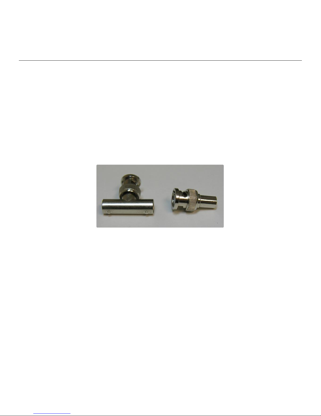
If you are using a high input impedance oscilloscope to monitor the PulseBlasterDDS-I-300's output, place a resistor
that matches the characteristic impedance of the transmission line in parallel with the coaxial transmission line at the
oscilloscope input by attaching it to the line through a T-Adapter(e.g., a 50 Ω resistor with a 50 Ω transmission line, see
Figures 3 and 4 below). For ease of observing the pulsed RF signals, the oscilloscope should be triggered by any of the
TTL outputs. When using an oscilloscope with an adjustable bandwidth, set the bandwidth to as large as possible. Failure
to do so may yield inaccurate readouts on the oscilloscope.
Figure 3: Left: BNC T-Adapter and Right: BNC 50 Ohm
resistor.
http://www.spincore.com 9 2017-11-14
 Loading...