

Page 1

TMS320F240
Evaluation Module
Technical
Reference
1998 DSP Development Systems
Page 2

TMS320F240
Evaluation Module
Technical Reference
503279-0001 Rev. C
June 1998
SPECTRUM DIGITAL, INC.
10853 Rockley Road Houston, TX. 77099
Tel: 281/561-6952 Fax: 281/561-6037
[email protected] www.spectrumdigital.com
Page 3

IMPORTANT NOTICE
Spectrum Digital, Inc. reserves the right to make changes to its products or to discontinue any
product or service without notice, and advises its customers to obtain the latest version of relevant
information to verify, before placing orders, that the information being relied on is current.
Spectrum Digital, Inc. warrants performance of its products and related software to current
specifications in accordance with Spectrum Digital’s standard w arranty. Testing and other quality
control techniques are utilized to the extent deemed necessary to support this warranty.
Please be aware that the products described herein are not intended for use in life-support
appliances, devices, or systems. Spectrum Digital does not warrant nor is liable for the product
described herein to be used in other than a development environment.
Spectrum Digital, Inc. assumes no liability for applications assistance, customer product design,
software performance, or infringement of patents or services described herein. Nor does Spectrum
Digital warrant or represent any license, either express or implied, is granted under any patent right,
copyright, or other intellectual property right of Spectrum Digital, Inc. covering or relating to any
combination, machine, or process in which such Digital Signal Processing development products or
services might be or are used.
WARNING
This equipment is intended for use in a laborato ry test environment only. It generates, uses, and can
radiate radio frequency energy and has not been tested for compliance with the limits of computing
devices pursuant to subpart J of part 15 of FCC rules, which are designed to provide reasonable
protection against radio frequency interference. Operation of this equipment in other environments
may cause interference with radio communications, in which case the user at his own expense will be
required to take whatever measures may be required to correct this interference.
TRADEMARKS
MS-DOS, MS-Windows, and Windows 95 are registered trademarks of Microsoft Corp
Copyright © 1997,1998 Spectrum Digital, Inc.
.
Page 4

Contents
1 Introduction to the TMS320F240 Ev aluation Module . . . . . . . . . . . . . . . . . . . . . . . . . . . . 1-1
Provides you with a description of the TMS320F240 Evaluation Module, key features, and
board outline.
1.0 Overview of the TMS320F240 EVM . . . . . . . . . . . . . . . . . . . . . . . . . . . . . . . . . . . . . . . . . 1-2
1.1 Key F eatures of the TMS320F240 EVM . . . . . . . . . . . . . . . . . . . . . . . . . . . . . . . . . . . . . 1-2
1.2 Functional Overview of the TMS320F240 EVM . . . . . . . . . . . . . . . . . . . . . . . . . . . . . . . . 1-3
2 TMS320F240 EVM Operation . . . . . . . . . . . . . . . . . . . . . . . . . . . . . . . . . . . . . . . . . . . . . . . . . 2-1
Describes the operation of the EVM320F240. Information is
interfaces.
2.0 The TMS320F240 EVM Operation . . . . . . . . . . . . . . . . . . . . . . . . . . . . . . . . . . . . . . . . . . 2-3
2.1 The TMS320F240 EVM Board . . . . . . . . . . . . . . . . . . . . . . . . . . . . . . . . . . . . . . . . . . . . 2-3
2.1.1 Pow er Connector . . . . . . . . . . . . . . . . . . . . . . . . . . . . . . . . . . . . . . . . . . . . . . . . . . . . . 2-4
2.2 TMS320C2XX Memory Interface . . . . . . . . . . . . . . . . . . . . . . . . . . . . . . . . . . . . . . . . . . . 2-4
2.2.1 Program Memory . . . . . . . . . . . . . . . . . . . . . . . . . . . . . . . . . . . . . . . . . . . . . . . . . . . . . . 2-5
2.2.2 Data Memory . . . . . . . . . . . . . . . . . . . . . . . . . . . . . . . . . . . . . . . . . . . . . . . . . . . . . . . . . . 2-8
2.2.3 I/O Space . . . . . . . . . . . . . . . . . . . . . . . . . . . . . . . . . . . . . . . . . . . . . . . . . . . . . . . . . . . . . 2-9
2.3 Onboard UART . . . . . . . . . . . . . . . . . . . . . . . . . . . . . . . . . . . . . . . . . . . . . . . . . . . . . . . . . . 2-9
2.4 Oscillator Selection . . . . . . . . . . . . . . . . . . . . . . . . . . . . . . . . . . . . . . . . . . . . . . . . . . . . . . 2-9
2.5 Digital to Analog Conversion . . . . . . . . . . . . . . . . . . . . . . . . . . . . . . . . . . . . . . . . . . . . . . 2-10
2.6 Expansion Bus . . . . . . . . . . . . . . . . . . . . . . . . . . . . . . . . . . . . . . . . . . . . . . . . . . . . . . . . 2-10
2.6.1 TMS320F240 EVM Expansion Connector . . . . . . . . . . . . . . . . . . . . . . . . . . . . . . . . . . 2-10
2.6.1.1 Expansion I/O Connector . . . . . . . . . . . . . . . . . . . . . . . . . . . . . . . . . . . . . . . . . . . . . . . 2-11
2.6.1.2 Expansion Analog Connector . . . . . . . . . . . . . . . . . . . . . . . . . . . . . . . . . . . . . . . . . . . 2-12
2.6.1.3 Expansion Address and Data Connector . . . . . . . . . . . . . . . . . . . . . . . . . . . . . . . . . . 2-13
2.6.1.4 Expansion Control Connector . . . . . . . . . . . . . . . . . . . . . . . . . . . . . . . . . . . . . . . . . . . 2-14
2.7 JTAG Interface . . . . . . . . . . . . . . . . . . . . . . . . . . . . . . . . . . . . . . . . . . . . . . . . . . . . . . . . . 2-15
2.8 On-Chip Asychronous Serial Port . . . . . . . . . . . . . . . . . . . . . . . . . . . . . . . . . . . . . . . . . 2-16
2.9 Onboard Serial Interface . . . . . . . . . . . . . . . . . . . . . . . . . . . . . . . . . . . . . . . . . . . . . . . . . 2-17
2.10 TMS320F240 EVM Jumpers . . . . . . . . . . . . . . . . . . . . . . . . . . . . . . . . . . . . . . . . . . . . . . 2-18
2.10.1 Jumper JP1, Enable/Disable Flash Programming . . . . . . . . . . . . . . . . . . . . . . . . . . . 2-19
2.10.2 Jumper JP2, Enable/Disable Internal ROM/FLASH . . . . . . . . . . . . . . . . . . . . . . . . . 2-19
2.10.3 Jumper JP3, Oscillator Source Select . . . . . . . . . . . . . . . . . . . . . . . . . . . . . . . . . . . . 2-20
2.10.4 Jumper JP4, Enable/Disable RTS to BIO-/IOPC3 . . . . . . . . . . . . . . . . . . . . . . . . . . . 2-20
2.10.5 Jumper JP5, Enable/Disable RXD to SCIRXD/IO . . . . . . . . . . . . . . . . . . . . . . . . . . . 2-21
2.10.6 Jumper JP6, VREFHI Source Select . . . . . . . . . . . . . . . . . . . . . . . . . . . . . . . . . . . . . 2-21
2.10.7 Jumper JP7, VREFLO Source Select . . . . . . . . . . . . . . . . . . . . . . . . . . . . . . . . . . . . 2-22
2.10.8 Jumper JP8, UAR T Interrupt Select . . . . . . . . . . . . . . . . . . . . . . . . . . . . . . . . . . . . . . 2-22
2.10.9 Jumper JP9, A15 Select . . . . . . . . . . . . . . . . . . . . . . . . . . . . . . . . . . . . . . . . . . . . . . 2-23
2.10.10 Jumper JP10, Not Used . . . . . . . . . . . . . . . . . . . . . . . . . . . . . . . . . . . . . . . . . . . . . 2-23
provided on the EVM’s various
Page 5

2.10.11 Jumper JP11, Enable/Disable Host Reset via DTR- . . . . . . . . . . . . . . . . . . . . . . . . . . . . . 2-23
2.10.12 Jumper JP12, Enable/Disable Memory Mapping . . . . . . . . . . . . . . . . . . . . . . . . . . . . . . . . 2-24
2.10.13 Jumper JP13, Not Used . . . . . . . . . . . . . . . . . . . . . . . . . . . . . . . . . . . . . . . . . . . . . . . . . . . . 2-24
2.10.14 Jumper JP14, Enable/Disable Onboard FLASH . . . . . . . . . . . . . . . . . . . . . . . . . . . . . . . . . 2-24
2.10.15 Jumper JP15, Onboard UART CTS Routing . . . . . . . . . . . . . . . . . . . . . . . . . . . . . . . . . . . . 2-25
2.11 LEDS . . . . . . . . . . . . . . . . . . . . . . . . . . . . . . . . . . . . . . . . . . . . . . . . . . . . . . . . . . . . . . . . . . . . . . 2-25
2.12 Resets . . . . . . . . . . . . . . . . . . . . . . . . . . . . . . . . . . . . . . . . . . . . . . . . . . . . . . . . . . . . . . .. . . . . . 2-25
2.13 Test P oint . . . . . . . . . . . . . . . . . . . . . . . . . . . . . . . . . . . . . . . . . . . . . . . . . . . . . . . . . . . . . . . . . . 2-25
A TMS320F240 EVM PAL Equations . . . . . . . . . . . . . . . . . . . . . . . . . . . . . . . . . . . . . . . . . . . . . . . . . . . . A-1
Lists the PAL equations that are used on the TMS320F240 EVM
A.1 Memory Decode PAL Equations . . . . . . . . . . . . . . . . . . . . . . . . . . . . . . . . . . . . . . . . . . . . . . . . . . . . A-2
A.2 Decode PAL Equations . . . . . . . . . . . . . . . . . . . . . . . . . . . . . . . . . . . . . . . . . . . . . . . . . . . . . . . . . . A-8
A.3 UART Control PAL Equations . . . . . . . . . . . . . . . . . . . . . . . . . . . . . . . . . . . . . . . . . . . . . . . . . . . . A-5
B TMS320F240 Schematics . . . . . . . . . . . . . . . . . . . . . . . . . . . . . . . . . . . . . . . . . . . . . . . . . . . . . . . . . . . B-1
Contains the schematics for the TMS320F240 EVM
C TL16C550 Data Sheet . . . . . . . . . . . . . . . . . . . . . . . . . . . . . . . . . . . . . . . . . . . . . . . . . . . . . . . . . . . . . C-1
Contains the technical information for the TL16C550
D MP7680 DAC Pr ogramming Inf ormation . . . . . . . . . . . . . . . . . . . . . . . . . . . . . . . . . . . . . . . . . . . . . . . D-1
Contains information regarding the programming of the MP7680 Digital-to-Analog Converter.
D .1 MP7680 Digital-to Analog Con v erter . . . . . . . . . . . . . . . . . . . . . . . . . . . . . . . . . . . . . . . . . . . . . . . . D-2
D.2 MP7680 Prog ramming . . . . . . . . . . . . . . . . . . . . . . . . . . . . . . . . . . . . . . . . . . . . . . . . . . . . . . . . . . D-3
D .3 MP7680 Calibr ation Considerations . . . . . . . . . . . . . . . . . . . . . . . . . . . . . . . . . . . . . . . . . . . . . . . D-3
Page 6

About This Manual
This document describes the board level operations of the TMS320F240 evaluation
module (EVM). The EVM is based on the Texas Instruments TMS320F240 Digital
Signal Processor .
The TMS320F240 EVM is a table top card to allow engineers and software developers
to evaluate certain characteristics of the TMS320F240 DSP to determine if the
processor meets the designers application requirements. Evaluators can create
software to execute onboard or expand the system in a variety of ways.
Notational Conventions
This document uses the following conventions.
The TMS320F240 will sometimes be referred to as the F240 or C24X.
Program listings, program examples, and interactive displays are shown is a special
italic typeface. Here is a sample program listing.
equations
!rd = XXXXXXXXXXX;
Information About Cautions
This book may contain cautions.
This is an example of a caution statement.
A caution statement describes a situation that could potentially damage your software,
or hardware, or other equipment. The information in a caution is provided for your
protection. Please read each caution carefully.
Related Documents
Texas Instruments TMS320F240 Users Guide
Texas Instruments TMS320 Fixed Point Assembly Language Users Guide
Texas Instruments TMS320 Fixed Point C Language Users Guide
Texa s Instruments TMS320 Fixed Point C Source Debugger Users Guide
Page 7

Chapter 1
Introduction to the TMS320F240
Evaluation Module
This chapter provides you with a description of the TMS32F240 Evaluation
Module along with the key features and a block diagram of the circuit
board.
Topic Page
1.0 Overview of the TMS320F240 EVM 1-2
1.1 Key Features of the TMS320F240 EVM 1-2
1.2 Functional Overview of the TMS320F240 EVM 1-3
1-1
Page 8

Spectrum Digital, Inc
1.0 Overview of the TMS320F240 EVM
The TMS320F240 evaluation module(EVM) is a stand-alone card that lets evaluators
examine certain characteristics of the F240 digital signal processor(DSP) to determine
if this DSP meets their application requirements. Furthermore, the module is an
excellent platform to develop and run software on the F240 family of processors.
The F240 EVM is shipped with a TMS320F240 DSP however other family members
can be placed in the on board socket as they become available. The EVM allows full
speed verification of F240 code. With 544 w ords of onchip data me mory, 128K words of
onboard memory, flash rom, on chip UART, on board UART, and an MP7680 Digital
to Analog Converter, the board can solve a variety of problems as shipped. Four
expansion connectors are provided to interface to any necessary evaluation circuitry
not provided on the as shipped configuration.
To simplify code develop and shorten debugging time a number of user interfaces ar e
available.
1.1 Key Features of the TMS320F240 EVM
The F240 EVM has the following features:
• F240 operating at 20 MIPS with 128K words of zero wait state memory
• MP7680 Four(4) Channel Digital to Analog converter
• On Chip UART with RS232 Drivers
• 32K words of onchip Flash ROM
• Second on board UART
• 32K words of on board Flash ROM
• 4 Expansion Connectors (data, address, I/O, and control)
• On board IEEE 1149.1 JTAG Connection for Optional Emulation
• 5 Volt Only Operation
1-2
TMS320F240 Evaluation Module Technical Reference
Page 9
Spectrum Digital, Inc
1.2 Functional Overview of the TMS320F240 EVM
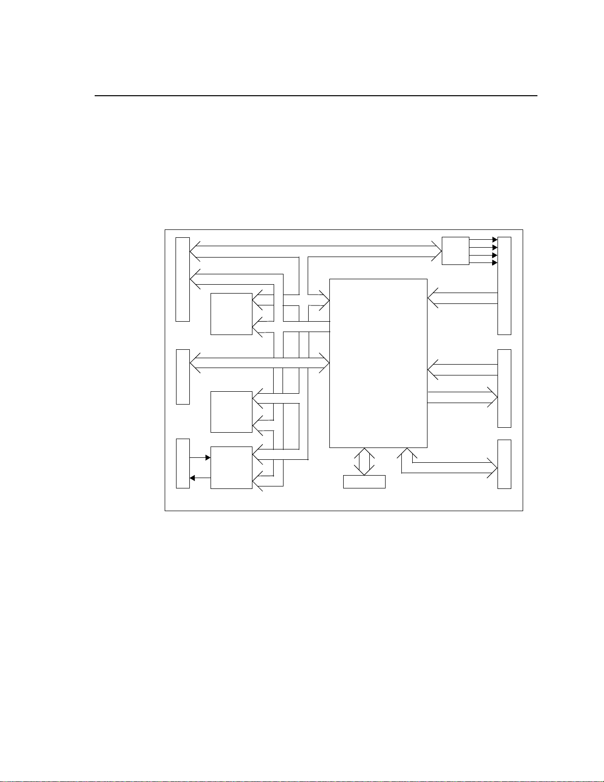
Figure 1-1 shows a block diagram of the basic configuration for the F240 EVM. The
major interfaces of the EVM include the target ram and rom interface, target UART,
analog interface, and expansion interface.
The F240 interfaces to 128K Words of zero wait-state static memory. An external I/O
interface supports 65,000 parallel I/O ports and optional high speed synchronous serial
port. A Flash Boot Rom can be mapped into the memory interface.
A
D
D
R
E
S
S
/
D
A
T
A
P
3
C
O
N
T
R
O
L
P
4
SRAM
128K x 16
FLASH
DATA
ADDRESS
TMS320F240
CONTROL
ANALOG
PWM/IO
MP7680
D/A
I/O
EPROM
32K x 16
S
E
R
I
A
L
P
7
TL16C550
UART
JTAG UART
JTAG P5
A
N
A
L
O
G
E
X
P
A
N
S
I
O
N
P
2
I
/
O
E
X
P
A
N
S
I
O
N
P
1
S
E
R
I
A
L
P
6
Figure 1-1 BLOCK DIAGRAM TMS320F240 EVM
1-3
Page 10

Spectrum Digital, Inc
1-4
TMS320F240 Evaluation Module Technical Reference
Page 11

Chapter 2
Operation of the TMS320F240
Evaluation Module
This chapter describes the operation of the TMS32F240 Evaluation
Module along with the key interfaces and an outline of the circuit board.
Topic Page
2.0 The TMS320F240 EVM Operation 2-3
2.1 The TMS320F240 EVM Board 2-3
2.1.1 Power Connector 2-4
2.2 TMS320F240 Memory Interface 2-4
2.2.1 Program Memory 2-5
2.2.2 Data Memory 2-8
2.2.3 I/O Space 2-9
2.3 Onboard UART 2-9
2.4 Oscillator Selection 2-9
2.5 Digital to Analog Conversion 2-10
2.6 Expansion Bus 2-10
2.6.1 TMS320F240 EVM Expansion Connector 2-10
2.6.1.1 Expansion I/O Connector 2-11
2.6.1.2 Expansion Analog Connecto r 2-12
2.6.1.3 Expansion Address and Data Connector 2-13
2.6.1.4 Expansion Control Connector 2-14
2.7 JTAG Interface 2-15
2.8 On-Chip Asynchronous Serial Port 2-16
2.9 Onboard Serial Interface 2-17
2-1
Page 12

Spectrum Digital, Inc
Topic Page
2.10 TMS320F240 EVM Jumpers 2-18
2.10.1 Jumper JP1, Enable/Disable Flash Programming 2-19
2.10.2 Jumper JP2, Enable/Disable Internal ROM/FLASH 2-19
2.10.3 Jumper JP3, Oscillator Source Select 2-20
2.10.4 Jumper JP4, Enable/Disable RTS to BIO-/IOPC3 2-20
2.10.5 Jumper JP5, Enable/Disable RXD to SCIRXD/IO 2-21
2.10.6 Jumper JP6, VREFHI Source Select 2-21
2.10.7 Jumper JP7, VREFLO Source Select 2-22
2.10.8 Jumper JP8, UART Interrupt Select 2-22
2.10.9 Jumper JP9, A15 Select 2-23
2.10.10 Jumper JP10, Not Used 2-23
2.10.11 Jumper JP11, Enable/Disable Host Reset via DTR- 2-23
2.10.12 Jumper JP12, Enable/Disable Memory Mapping 2-24
2.10.13 Jumper JP13, Not Used 2-24
2.10.14 Jumper JP14, Enable/Disable Onboard FLASH 2-24
2.10.15 Jumper JP15, Onboard UART CTS Routing Jumper 2-25
2.11 LEDS 2-25
2.12 Resets 2-25
2.13 Test Point 2-25
2-2
TMS320F240 Evaluation Module Technical Reference
Page 13
Spectrum Digital, Inc
2.0 The TMS320F240 EVM Operation
This chapter describes the F240 Evaluation module, its key components, and how they
operate. It also provides information on the EVM’s various interfaces.The F240 EVM
consists of six major blocks of logic.
• F240 external memory
• Analog Interface
• On Chip Serial Interface
• On board Serial I/O interface
• Expansion interface
• JTAG Interface
2.1 The TMS320F240 EVM Board
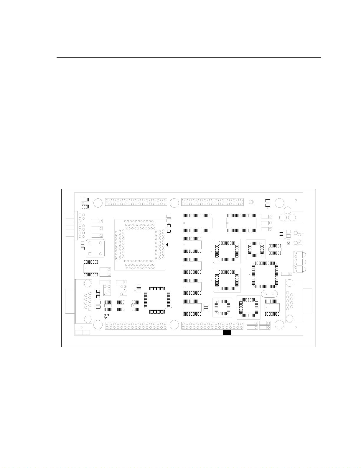
The F240 EVM is a 3U sized board which is powered by an external 5 Volt only power
supply. Figure 2-1 shows the layout of the F240 EVM.
P1 P3
U1
1
P5
L1 U2
U3
11
JP1
1
JP2
1
JP3
1
JP4
JP5
JP6
P6
L2
C1
11
R34
U5 U7
D1
11
I/O ADDRESS/DATA
SPECTRUM DIGITAL
INCORPORATED
TMS320F240 EVM
JP7
C2
R23
U6
ANALOG CONTROL
PWB 503271 REV B
C3
L3
U10
U4
U11
U12
U8
U13
P4P2
ASSY 503270 REV
Figure 2-1 TMS32F240 EVM
U9 U14
U15
U16
U17
C4
JP11
U19
TP1
U18
JP13
C5
JP8
1
1
JP9
1
L4
JP10
U21
U20
Y1
U22
JP12
11
JP14
+5V
J1
C6
SW1
D2
DS1
DS2
JP15
DS3
1
P7
2-3
Page 14

Spectrum Digital, Inc
2.1.1 Power Connector
The F240 is powered by a 5 Volt only power supply which is available with the module.
The board requires 750 milliamps. The power is supplied via 2 millimeter jack J1. If
expansion boards are connected to the mo dule a higher amperage power supply ma y
be necessary.
2.2 TMS320F240 Memory Interface
The EVM includes 64k Words of zero wait-state program ram memory and 64k words
of zero wait-state data ram memory, pr oviding a total of 128 k words of off chip static
ram. The board also features 2 sockets for flash rom.
It is important to remember that internal memory has a higher precedence than the
external memory. For more information on the memory in the device populated in your
EVM card please refer to Texas Instruments TMS320F240 Users Guide. Futhermore,
it is important to take into account that external memory is affected by wait-states. Wait
state generation for off-chip memory space (data, program, or I/O) is done with the
Wait State Generation Registe r(WSGR). To obtain zero waitstate off-chip memory
bits in the WSGR must be appropriately programmed. Th e board powers up with 1
wait-state. The EVM board does not generate wait states via the ready signal for
external program and data memory accesses.
External memory decode is done via U19 a GAL20V8. The generic array de vice selects
the RAM, FLASH ROM, or on board peripherals. The equations for the GAL are
included in Appendix A. The figure below shows a zero wait state program space
memory read followed by a data space memory write.
2-4
TMS320F240 Evaluation Module Technical Reference
Page 15

Spectrum Digital, Inc
CLKOUT
ADDRESS
DA TA
R/W
PS-
DS-
STRB-
RAMOE-
RAMWE-
The external Flash ROM is mapped into the program space. Note that this memory
requires multiple wait states. The main purpose of this memory is to allow for the boot
loading of programs without the need of programming the processors internal flash.
2.2.1 Program Memory
READ WRITE
Zero Wait State Memory Timing
There are several configurations for program memory. The selection of these
configurations is done by the position of jumpers JP2 and JP14. If JP2 is in the 2-3
position then the DSP is in microcomputer mode and the internal memory is enabled
from 0x0000 to 0x3fff. If JP2 is in position 1-2 then the internal FLASH/ROM is disabled
and this address range is available to external memory.
External program memory is controlled by jumper JP14. When JP14 is configured in
the 1-2 position external RAM is enabled from 0x0000-0xffff. Remember internal
memory takes precedence over external memory. If JP14 is in position 2-3 the external
FLASH is enabled from 0x000-0x7fff. If enabled it is possible to select and deselect the
external FLASH memory by writing to bits D3 and D2 in the UART’S MCR register. For
instance you can set the configuration to Out2 = 0 and Ou t1 = 1 to copy the program
from FLASH to RAM at the same address.
2-5
Page 16

Spectrum Digital, Inc
Table 1: FLASH/RAM CONFIGURATION
UART MCR BITs
D3(Out2) D2(Out1)
00FLASH*
0 1 FLASH RAM
1 0 RAM FLASH
11RAMRAM
* Power up configuration
Note: The bits in the MCR register are inverted from
what appears on the output pins.
FUNCTION
READ WRITE
2-6
TMS320F240 Evaluation Module Technical Reference
Page 17

Spectrum Digital, Inc
Shown below are the four program memory configurations:
Program Space
MP/MC- = 1, JP2(1-2)
Microprocessor Mode
External FLASH, JP14(2-3)
Hex
0000
003F
0040
7FFF
8000
FDFF
FE00
FEFF
FF00
FFFF
0000
003F
0040
Interrupts
(On-chip)
External FLASH
External RAM
On-Chip DARAM
B0 (CNF = 1)
External (CNF = 0)
On-Chip DARAM
B0’ (CNF = 1)
External (CNF = 0)
Program Space
MP/MC- = 1, JP2(1-2)
No external FLASH, JP14(1-2)
Interrupts Interrupts
(On-chip)
RAM
External RAM
Program Space
MP/MC- = 0, JP2(2-3)
Microcomputer Mode
External FLASH, JP14(2-3)
Hex
0000
003F
0040
3FFF
4000
7FFF
8000
FDFF
FE00
FEFF
FF00
FFFF
Hex
0000
003F
0040
3FFF BOOTPROT pin)
4000
Interrupts
(On-chip)
On-chip ROM
(Flash EEPROM)
(8x2K Segments)
(Seg 0 = Boot Seg
@ 0h-07FFh by
BOOTPROT pin)
External FLASH
External RAM
On-Chip DARAM
B0 (CNF = 1)
External (CNF = 0)
On-Chip DARAM
B0’ (CNF = 1)
External (CNF = 0)
Program Space
MP/MC- = 0, JP2(2-3)
Microcomputer ModeMicroprocessor Mode
No external FLASH, JP14(1-2)
(On-chip)
On-chip ROM
(Flash EEPROM)
(8x2K Segments)
(Seg 0 = Boot Seg
@ 0h-07FFh by
External RAM
FDFF
FE00
FEFF
FF00
FFFF
On-Chip DARAM
B0 (CNF = 1)
External (CNF = 0)
B0’ (CNF = 1)
External (CNF = 0)
FDFF
FE00
FEFF
FF00
FFFF
On-Chip DARAM
B0 (CNF = 1)
External (CNF = 0)
On-Chip DARAMOn-Chip DARAM
B0’ (CNF = 1)
External (CNF = 0)
2-7
Page 18

Spectrum Digital, Inc
2.2.2 Data Memory
The two data memory configurations are configured by jumper JP12. Configured in the
1-2 position the external RAM is enabled from 0x8000-0xffff. Loading the GREG
register will disable all or part the external memory, depending on the value, and allow
devices connected to the expansion bus to be accessed.
When JP12 is configured in the 2-3 position and jumper JP9 is also configured in the
2-3 position then the setting of the GREG register is used to remap the unused 32K of
RAM into the memory map. In this mode BR- is used to invert address A15. In other
words if BR- is inactive address 0x8000 would map to address 0x8000 in the RAM. If
BR- was active then address 0x8000 would be mapped to 0x0000 in the data RAM.
Hex
0000
005F
0060
007F
0080
00FF
0100
01FF
0200
02FF
0300
03FF
0400
04FF
0500
07FF
0800
6FFF
7000
73FF
7400
743F
7440
77FF
7800
7FFF
8000
FFFF
Data Space
Memory-Mapped
Register and
Reserved
On-Chip
DARAM B2
Reserved
On-Chip DARAM
B0 (CNF = 0)
Reserved (CNF = 1)
On-Chip DARAM
B0’ (CNF = 0)
Reserved (CNF = 1)
On-Chip
DARAM B1
On-Chip
DARAM B1’
Reserved
Illegal
Peripheral MemoryMapped Registers
(System, ADC, SCI,
SPI, I/O, Interrupts)
Peripheral MemoryMapped Registers
(Event Manager)
Reserved
Illegal
External RAM
2-8
TMS320F240 Evaluation Module Technical Reference
Page 19

Spectrum Digital, Inc
2.2.3 I/O Space
The I/O map for the TMS320F240 EVM is shown below:
2.3 Onboard UART
The TMS320F240 EVM has a TL16C550 UART mapped into the I/O space of the F240
at locations 0x0010 - 0x0018. The UART allows users to use this resource for data
logging, code debugging or other application features. Appendix C contains the
programming information for the TL16C550 device.
2.4 Oscillator Selection
Hex
0000
0004
0005
000F
0010
0018
0019
FEFF
FF00
FFFF
I/O Space
D/A Converter
Reserved
Off-Chip UART
External
Reserved
The TMS320F240 EVM is equipped with a 10 Megahertz oscillator. When the
processor resets the PLL Clock Module defaults to CLKIN/2 yielding a 5 Mhz clkout.
The user should refer to the “PLL Clock Module” section in the TMS320F240 User’s
guide for valid clock configurations.
2-9
Page 20

Spectrum Digital, Inc
2.5 Digital to Analog Converter
The TMS320F240 EVM provides four(4) 12-bit D/A channels. The output is from 0 to 5
volts DC. The con v erter is mapped into I/O address space 0x0000 to 0x0004. Lo cations
0x0000 through 0x0003 are used for the data holding registers for channels 1-4
respectively. I/O address 0x0004 is used to transfer values in the holding registers to
the converters. For instance y ou can write to the 4 holding registers and transfer all 4 to
the converters at the same time. Information about programming this converter can be
found in appendix D.
Table 2: DAC I/O Addresses
I/O Address Channel #
0x0000 1
0x0001 2
0x0002 3
0x0003 4
0x0004 Transfer
2.6 Expansion Bus
The TMS320F240 EVM has an expansion bus which brings out all of the signals from
the DSP. This expansion bus allows the user to design custom circuitry to be used with
his application without having to design a CPU card. In addition this interface is used b y
Spectrum Digital for all of its add-on modules.
2.6.1 TMS320F240 EVM Expansion Connector
Expansion boards interface to the TMS320F240 EVM via an expansion bus.
This expansion bus is divided into 4 double row header connectors. This se ction
contains the signal definitions and pin numbers for each of the connectors.
2-10
TMS320F240 Evaluation Module Technical Reference
Page 21

Spectrum Digital, Inc
2.6.1.1 Expansion I/O Connector
The definition of P1, which has the I/O signals is shown below.
Table 3: P1 I/O
Pin # Signal Pin # Signal
1 VCC, +5 Volts 2 VCC, +5 Volts
3 PWM1/CMP1 4 PWM2/CMP2
5 PWM3/CMP3 6 PWM4/CMP4
7 PWM5/CMP5 8 PWM6/CMP6
9 PWM7/CMP7/IOPB0 10 PWM8/CMP8/IOPB1
11 PWM9/CMP9/IOPB2 12 T1PWM/T1CMP/IOPB3
13 T2PWM/T2CMP/IOPB4 14 T3PWM/T2CMP/IOPB5
15 TMDIR/IOPB6 16 TRMCLK/IOPB7
17 GND 18 GND
19 XF/IOPC2 20 BIO-/IOPC3
21 CAP1/QEP1/IOPC4 22 CAP2/QEP2/IOPC5
23 CAP3/IOPC6 24 CAP4/IOPC7
25 RESERVED 26 PDPINT27 SCITXD/IO 28 SCIRXD/IO
29 SPISIMO/IO 30 SPISOMI/IO
31 SPICLK/IO 32 SPISTE/IO
33 GND 34 GND
2-11
Page 22

Spectrum Digital, Inc
2.6.1.2 Expansion Analog Connector
The definition of P2, which has the analog signals is shown below.
Pin # Signal Pin # Signal
1 VCCA, +5V Analog 2 VCCA, +5V Analog
3 ADC IN0/IO PA0 4 ADCIN1/IOPA1
5 ADCIN2 6 ADCIN3
7 ADCIN4 8 ADCIN5
9 A DCIN 6 10 ADCIN7
11 ADCIN8/IOPA3 12 ADCIN9/IOPA2
13 ADCIN10 14 ADCIN11
15 ADCIN12 16 ADCIN13
17 AGND 18 AGND
19 ADCIN14 20 ADCIN15
21 VREFHI 22 VREFLO
Table 4: P2 Analog
23 AGND 24 AGND
25 DACOUT1 26 DACOUT2
27 DACOUT3 28 DACOUT4
29 RESERVED 30 RESERVED
31 RESERVED 32 ADCSOC/IOPC0
33 AGND 34 AGND
2-12
TMS320F240 Evaluation Module Technical Reference
Page 23

Spectrum Digital, Inc
2.6.1.3 Expansion Address and Data Connector
The definition of P3, which has the address and data signals is shown below .
Table 5: P3 Address/Data
Pin # Signal Pin # Signal
1A02A1
3A24A3
5A46A5
7A68A7
9 A810A9
11A1012A11
13A1214A13
15A1416A15
17 GND 18 GND
19 D0 20 D1
21 D2 22 D3
23 D4 24 D5
25 D6 26 D7
27 D8 28 D9
29D1030D11
31D1232D13
33D1434D15
2-13
Page 24

Spectrum Digital, Inc
2.6.1.4 Expansion Control Connector
The definition of P4, which has the control signals is shown below.
Pin # Signal Pin # Signal
1 VCC, +5 Volts 2 VCC, +5 Volts
3 DS- 4 PS5IS-6BR7 WE- 8 W/R-
9STRB-10 R/W
11 READY 12 RESERVED
13 RS- 14 TRGRESET15 NMI- 16 XINT117 GND 18 GND
19 XINT2-/IO 20 XINT3-/IO
21 RESERVED 22 RESERVED
Table 6: P4 Control
23 RESERVED 24 RESERVED
25 RESERVED 26 RESERVED
27 RESERVED 28 RESERVED
29 RESERVED 30 RESERVED
31 CLKIN 32 CLKOUT/IOPC1
33 GND 34 GND
2-14
TMS320F240 Evaluation Module Technical Reference
Page 25

Spectrum Digital, Inc
2.7 JTAG Interface.
The TMS320F240 Evaluation Module is supplied with a 14 pin header interface, P5.
This is the standard interface used by JTAG emulators to interface to Texas
Instruments DSPs. The pinout for the connector is shown below:
TMS
TDI
PD (+5V)
TDO
TCK-RET
TCK
EMU0
12
3
56
7
9
11
13
TRST-
4
GND
no pin (key)
GND
8
GND
10
GND
12
EMU1
14
Header Dimensions
Pin-to-Pin spacing, 0.100 in. (X,Y)
Pin width, 0.025-in. square post
Pin length, 0.235-in. nominal
2-15
Page 26

Spectrum Digital, Inc
2.8 On-Chip Asynchronous Serial Port
The TMS320F240 DSP has an on-chip asynchronous serial port. This port is brought
out to connector P6 on the EVM320F240. Connector P6 is a DB9 fema le connector.
This RS232 connector allows the user to connect an e xternal instrument or computer to
the EVM320F240. This means data can be logged or commands given to the control
algorithm. The user should refer to documentation on jumpers JP4 and JP5 prior to
using this serial port. The pin positions for the P6 connector as view ed from the edg e of
the EVM320F240.
The pin numbers and their corresponding signals are shown in the table below:
Table 7: P6 RS232 Pinout
Pin # PC (female) SD EVM
5
3
4
8
9
1
2
7
6
2 Rx, input Tx, output
3 Tx, output Rx, input
4 DTR, output Reset/CTS,
input
5GND GND
8 CTS, input RTS, output
2-16
TMS320F240 Evaluation Module Technical Reference
Page 27

Spectrum Digital, Inc
2.9 Onboard Serial Interface
The EVM320F240 has a TL16C550 UART which provides an additional serial
interface. This UART is mapped into I/O space at locations 0x0010 to 0x0018.
This device allows users to use this reso urce for data logging, code debugging and
other applications.
NOTE:
To use the UART you must enable the clockout of the F240.
You must also make sure the number of wait states is set correctly
in the WSGR register.
This UART is brought out to connector P7 on the EVM320F240. Connector P7 is a
DB9 female connector. The pin positions for th e P4 connector as viewed from the edge
of the EVM320F240.
5
3
4
9
The pin numbers and their corresponding signals are shown in the table below:
1
2
8
7
6
Table 8: P7 RS232 Pinout
Pin # PC (female) SD EVM
2 Rx, input Tx, output
3 Tx, output Rx, input
4 DTR, output Reset/CTS,
input
5GND GND
8 CTS, input RTS, output
Jumper JP11 allows the generation of a system reset from the serial port. If jumper JP11 is in
the 1-2 position a reset will occur when the DTR- signal is brought active low.
2-17
Page 28
Spectrum Digital, Inc
2.10 TMS320F240 EVM Jumpers
The TMS320F240 EVM has 14 jumpers which determine how fe atures on the
EVM are utilized. The table below lists the jumpers and their function. The following
sections describe the use of each jumper.
Jumper # Size Function
JP1 1 x 3 Enable/Disable Flash Programming
JP2 1 x 3 Enable/Disable Internal ROM/FLASH
JP3 1 x 3 Oscillator Source Select
JP4 1 x 3 Enable/Disable RTS to BIO-/IOPC3
JP5 1 x 3 Enable/Disable RXD to SCIRXD/IO
JP6 1 x 3 VREFHI Source Select
JP7 1 x 3 VREFLO Source Select
JP8 1 x 3 UART Interrupt Select
JP9 1 x 3 A15 Source Select
JP10 1 x 3 Not Used
JP11 1 x 2 Enable/Disable Host Reset via DTRJP12 1 x 3 Enable/Disable Memory Mapping
JP13 1 x 3 Not Used
JP14 1 x 3 Enable/Disable Onboard FLASH
JP15 1 x 3 Onboard UART CTS Routing
Table 9: Jumpers
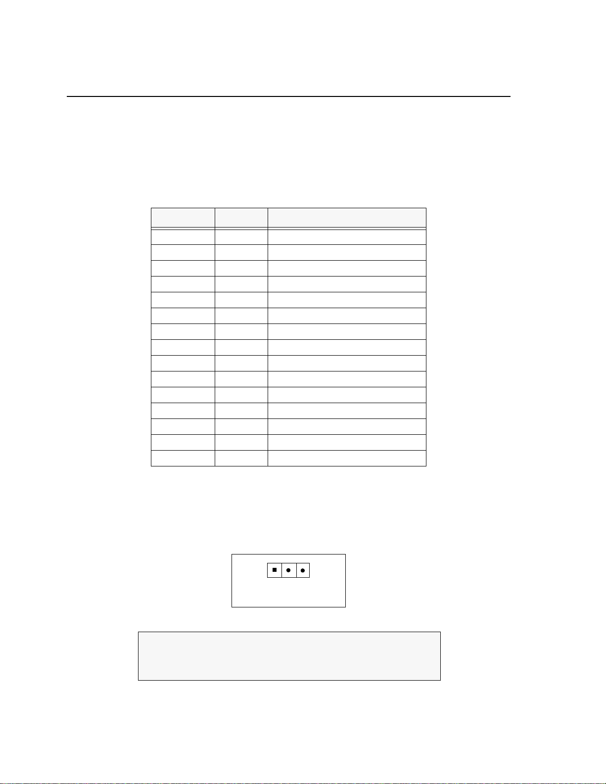
Each jumper on the TMS320F240 EVM is a 1x3 jumper. Each jumper must have the
selection 1-2 or 2-3. The #2 pin is the center pin. The #1 pin has a square solder pad
and can be seen from the solder side of the printed circuit board. This pin is usually
marked with a ‘1’ on the boards silkscreen. A top view of this type of jumper is shown
below:
2-18
312
1x3 Jumper Layout
WARNING !
Unless noted otherwise, all jumpers must be
installed in either the 1-2 or 2-3 position
TMS320F240 Evaluation Module Technical Reference
Page 29

Spectrum Digital, Inc
2.10.1 Jumper JP1, Enable/Disable Flash Programming
Jumper JP1 is connected to the VCCP pin of the TMS320F240. On the F240 device
this pin enables the programming of the internal flash memory. It also allows disabling
the watchdog timer module. Refer to the F240 User’s Guide for the programming
sequence to disable the watchdog timer. The table below shows the positions and their
functions:
Table 10: Jumper JP1
Position Function
1-2 Disable Flash Programming
2-3 Enable Flash Programming
2.10.2 Jumper JP2, Enable/Disable Internal ROM/FLASH
Jumper JP2 is connected to the MP/MC- pin on the TMS320F240. When the jumper is
in position 1-2 the internal ROM/FLASH is disabled. If the shorting plug is in the 2-3
position the internal memory is then enabled. The table below shows the positio ns and
their functions:
Table 11: Jumper JP2
Position Function
1-2 Internal ROM/FLASH disabled
(microprocessor mode)
2-3 Internal ROM/FLASH enabled
(microcomputer mode)
2-19
Page 30

Spectrum Digital, Inc
2.10.3 Jumper JP3, Oscillator Source Select
Jumper JP3 is used to select the source of the TMS320F240 Clockin. Jumper position
1-2 selects the onboard oscillator. If position 2-3 is used the clock is from pin 31 on the
Control connector P4. The table below shows the positions and their functions:
Table 12: Jumper JP3
Position Function
1-2 Selects Onboard Oscillator
2-3 Selects Pin 31 on Control
connector P4
2.10.4 Jumper JP4, Enable/Disable RTS to BIO-/IOPC3
Jumper JP4 enables the serial port P6 RTS- to the DSP’s BIO-/IOPC3 pin. Using
position 1-2 disables this feature, while position 2-3 enables it.
Note:
If this feature is enabled(2-3) then you must not drive the BIO-/IOPC3 pin from the
Control connector P4
.
The table below shows the positions and their functions:
2-20
Table 13: Jumper JP4
Position Function
1-2 Disables P6 RTS-
to BIO-/IOPC3
2-3 Enables P6 RTS- to
BIO-/IOPC3
TMS320F240 Evaluation Module Technical Reference
Page 31

Spectrum Digital, Inc
2.10.5 Jumper JP5, Enable/Disable RXD to SCIRXD/IO
Jumper JP5 enables the serial port P6 RXD to the DSP’ s SCIRXD/IO pin. If positio n 1-2
is selected this features is enabled. Selecting position 2-3 disables this feature.
Note:
If this feature is enabled(1-2) then you
Control connector P4.
The table below shows the positions and their functions:
2.10.6 Jumper JP6, VREFHI Select
must not
Table 14: Jumper JP5
Position Function
1-2 Enables P6 RXD to
DSP SCIRXD/IO
2-3 Disables P6 RXD
to DSP SCIRXD/IO
drive the SCIRXD/IO pin from the
Jumper JP6 is used to select the source for the VREFHI pin on the TMS320F240.
Position 1-2 selects the VCCA power which is +5 volts. If position 2-3 is used trim pot
R34 is used which allows a variable VREF High from 0-5 volts. The table below shows
the positions and their functions:
Table 15: Jumper JP6
Position Function
1-2 VCCA (+5V VrefH)
2-3 Trim Pot R34 (0-5V
VrefH)
2-21
Page 32

Spectrum Digital, Inc
2.10.7 Jumper JP7, VREFLO Select
Jumper JP7 is used to select the source for the VREFLO pin on the TMS320F240.
Positio n 1-2 selects the Analog ground. If position 2-3 is used trim pot R23 is used
The table below sho w s the positions and their functions:
Table 16: Jumper JP7
Position Function
1-2 Analog Ground
2-3 Trim Pot R23
2.10.8 Jumper JP8, UART Interrupt Select
Jumper JP8 selects the interrupt for the onboard UART. Position 1-2 selects NMI- while
position 2-3 selects the XINT1- pin. If you want to use both of these interrupts from
Control connector P4 then neither position should be selected. The table below shows
the positions and their functions:
(VrefL)
(0-5V VrefL)
Table 17: Jumper JP8
Position Function
1-2 Selects NMI- as
UART Interrupt
2-3 Selects XINT1- as
UART Interrupt
2-22
TMS320F240 Evaluation Module Technical Reference
Page 33

Spectrum Digital, Inc
2.10.9 Jumper JP9, A15 Source Select
Jumper JP9 is used to select the source for the memory’s A15 signal. When position
1-2 is used the TMS320F240’s A15 is used. The 2-3 position selects a mapping signal
from PAL U19. Refer to the memory section for details. The table below shows the
positions and their functions:
Table 18: Jumper JP9
Position Function
1-2 TMS320F240 A15
2-3 Mapped A15
2.10.10 Jumper JP10
Jumper JP10 is not used at this time.
2.10.11 Jumper JP11, Enable/Disable Host Reset via DTR-
Jumper JP11 allows the generation of system resets from the serial port P7. When
position 1-2 is used this feature is enabled meaning the system is reset when pin 4
(DTR-) is pulled low. This feature is disabled when position 2-3 is used. The table
below shows the positions and their functions:
Table 19: Jumper JP11
Position Function
1-2 Reset from P4, pin4
(DTR-) enabled
2-3 Disabled
2-23
Page 34

Spectrum Digital, Inc
2.10.12 Jumper JP12, Enable/Disable Memory Mapping
Jumper JP12 enables the address 15 mapping feature. Using position 2-3 enables this
feature. If position 1-2 is u sed the feature is disabled. Refer to the Data Memory section
on the use of this feature. The table below shows the positions and their functions:
Table 20: Jumper J12
Position Function
1-2 A15 Mapping Disabled
2-3 A15 Mapping Enabled
2.10.13 Jumper JP13
Jumper JP13 is not used at this time.
2.10.14 Jumper JP14, Enable/Disable Onboard Flash
Jumper JP14 is used to enable the onboard flash memory. Connecting positions 2-3
enables the onboard flash while position 1-2 disables it. Refer to the Program Memory
Section for the use of this feature. The table below shows the positions and their
functions:
2-24
Table 21: Jumper J14
Position Function
1-2 Disables onboard
flash memory
2-3 Enables onboard
flash memory
TMS320F240 Evaluation Module Technical Reference
Page 35

Spectrum Digital, Inc
2.10.15 Onboard UART CTS Routing Jumper, JP15
Jumper JP15 is used to configure the source of the CTS signal on the onboard UART.
When position 1-2 is used the pin 4 on P7 is used as the CTS input. If position 2-3 is
chosen pin 7 on P7 is used as the CTS input.
Table 22: Onboard UART CTS Routing
JP15 Position CTS Routing
1-2 P7 pin 4 used on CTS input
2-3 P7 pin 7 used on CTS input
2.11 LEDs
The TMS320F240 EVM has three light emitting diodes. The are under software
control. DS3 is normally ‘on’ after reset.These are shown in the table below:
Table 23: LEDs
LED # Color Controlling Signal On Signal State
2.12 Resets
There are multiple resets for the TMS320F240 EVM. The first reset is the power on
reset which is generated by the U1. This device waits until power is within the specified
range before releasing the power on reset pin to the TMS320F240.
There is also a system reset RS- which is both input and output from the TMS320F240.
Internal conditions such as a watchdog time-out will cause the RS- pin to go low.
External sources such as the push button(SW1), Host reset pin 4 on P4, and pin p13
on the Control connector P4 can generate a reset condition.
2.13 Test Point
One test point is provided on the TMS320F240 EVM that is connected to the GND
plane. This is used for connecting a scope’s ground signal.
DS1 Red XF/IOPC2 on DSP 1
DS2 Yellow BIO-/IO PC3 on DSP 1
DS3 Green DTR- on external UART 0
2-25
Page 36

Spectrum Digital, Inc
2-26
TMS320F240 Evaluation Module Technical Reference
Page 37

Printed in U.S.A., June 1998
503279-0001 Rev. C
 Loading...