

Page 1

TMS320C6416 DSK
Technical
Reference
2003 DSP Development Systems
Page 2

TMS320C6416 DSK
Technical Reference
505945-0001 Rev. B
November 2003
12502 Exchange Drive, Suite 440 Stafford, TX. 77477
Tel: 281.494.4505 Fax: 281.494.5310
sales@spectrumdigital.com www.spectrumdigital.com
SPECTRUM DIGITAL, INC.
Page 3

IMPORTANT NOTICE
Spectrum Digital, Inc. reserves the right to make changes to its products or to discontinue any
product or service without notice. Customers are advised to obtain the latest version of relevant
information to verify that the data being relied on is current before placing orders.
Spectrum Digital, Inc. warrants performance of its products and related software to current
specifications in accordance with Spectrum Digital’s standard warranty. Testing and other quality
control techniques are utilized to the extent deemed necessary to support this warranty.
Please be aware that the products described herein are not intended for use in life-support
appliances, devices, or systems. Spectrum Digital does not warrant nor is Spectrum Digital liable for
the product described herein to be used in other than a development environment.
Spectrum Digital, Inc. assumes no liability for applications assistance, customer product design,
software performance, or infringement of patents or services described herein. Nor does Spectrum
Digital warrant or represent any license, either express or implied, is granted under any patent right,
copyright, or other intellectual property right of Spectrum Digital, Inc. covering or relating to any
combination, machine, or process in which such Digital Signal Processing development products or
services might be or are used.
WARNING
This equipment is intended for use in a laboratory test environment only. It generates, uses, and can
radiate radio frequency energy and has not been tested for compliance with the limits of computing
devices pursuant to subpart J of part 15 of FCC rules, which are designed to provide reasonable
protection against radio frequency interference. Operation of this equipment in other environments
may cause interference with radio communications, in which case the user at his own expense will be
required to take whatever measures necessary to correct this interference.
Copyright
© 2003 Spectrum Digital, Inc.
Page 4

Contents
1 Introduction to the TMS320C6416 DSK Module . . . . . . . . . . . . . . . . . . . . . . . . . . . . . . . 1-1
Provides you with a description of the TMS320C6416 DSK Module, key features, and
block diagram.
1.1 Key Features . . . . . . . . . . . . . . . . . . . . . . . . . . . . . . . . . . . . . . . . . . . . . . . . . . . . . . . . . . 1-2
1.2 Functional Overview . . . . . . . . . . . . . . . . . . . . . . . . . . . . . . . . . . . . . . . . . . . . . . . . . . . . 1-3
1.3 Basic Operation . . . . . . . . . . . . . . . . . . . . . . . . . . . . . . . . . . . . . . . . . . . . . . . . . . . . . . . . . 1-4
1.4 Memory Map . . . . . . . . . . . . . . . . . . . . . . . . . . . . . . . . . . . . . . . . . . . . . . . . . . . . . . . . . . 1-5
1.5 Configuration Switch Settings . . . . . . . . . . . . . . . . . . . . . . . . . . . . . . . . . . . . . . . . . . . . . 1-6
1.6 Power Supply . . . . . . . . . . . . . . . . . . . . . . . . . . . . . . . . . . . . . . . . . . . . . . . . . . . . . . . . . 1-6
2 Board Components . . . . . . . . . . . . . . . . . . . . . . . . . . . . . . . . . . . . . . . . . . . . . . . . . . . . . . . . 2-1
Describes the operation of the major board components on the TMS320C6416 DSK.
2.1 CPLD (programmable Logic) . . . . . . . . . . . . . . . . . . . . . . . . . . . . . . . . . . . . . . . . . . . 2-2
2.1.1 CPLD Overview . . . . . . . . . . . . . . . . . . . . . . . . . . . . . . . . . . . . . . . . . . . . . . . . . . . . 2-2
2.1.2 CPLD Registers . . . . . . . . . . . . . . . . . . . . . . . . . . . . . . . . . . . . . . . . . . . . . . . . . . . . . 2-3
2.1.3 USER_REG Register . . . . . . . . . . . . . . . . . . . . . . . . . . . . . . . . . . . . . . . . . . . . . . 2-3
2.1.4 DC_REG Register . . . . . . . . . . . . . . . . . . . . . . . . . . . . . . . . . . . . . . . . . . . . . . . . . . 2-4
2.1.5 Version Register . . . . . . . . . . . . . . . . . . . . . . . . . . . . . . . . . . . . . . . . . . . . . . . . . . 2-4
2.1.6 MISC Register . . . . . . . . . . . . . . . . . . . . . . . . . . . . . . . . . . . . . . . . . . . . . . . . . . . . . 2-5
2.2 Codec Interface . . . . . . . . . . . . . . . . . . . . . . . . . . . . . . . . . . . . . . . . . . . . . . . . . . . . . 2-6
2.3 SRAM Interface . . . . . . . . . . . . . . . . . . . . . . . . . . . . . . . . . . . . . . . . . . . . . . . . . . . . . 2-7
2.4 Flash ROM Interface . . . . . . . . . . . . . . . . . . . . . . . . . . . . . . . . . . . . . . . . . . . . . . . . 2-7
2.5 LEDs and DIP Switches . . . . . . . . . . . . . . . . . . . . . . . . . . . . . . . . . . . . . . . . . . . . . . 2-7
2.6 Daughter Card Interface . . . . . . . . . . . . . . . . . . . . . . . . . . . . . . . . . . . . . . . . . . . . . . 2-8
3 Physical Specifications . . . . . . . . . . . . . . . . . . . . . . . . . . . . . . . . . . . . . . . . . . . . . . . . . . . . 3-1
Describes the physical layout of the TMS320C6416 DSK and its connectors.
3.1 Board Layout . . . . . . . . . . . . . . . . . . . . . . . . . . . . . . . . . . . . . . . . . . . . . . . . . . . . . . . . 3-2
3.2 Connector Index . . . . . . . . . . . . . . . . . . . . . . . . . . . . . . . . . . . . . . . . . . . . . . . . . . . . 3-3
3.3 Expansion Connectors . . . . . . . . . . . . . . . . . . . . . . . . . . . . . . . . . . . . . . . . . . . . . . . . 3-3
3.3.1 J4, Memory Expansion . . . . . . . . . . . . . . . . . . . . . . . . . . . . . . . . . . . . . . . . . . . . . 3-4
3.3.2 J3, Peripheral Expansion . . . . . . . . . . . . . . . . . . . . . . . . . . . . . . . . . . . . . . . . . . . . 3-5
3.3.3 J1, HPI Expansion Connector . . . . . . . . . . . . . . . . . . . . . . . . . . . . . . . . . . . . . . . . 3-6
3.4 Audio Connectors . . . . . . . . . . . . . . . . . . . . . . . . . . . . . . . . . . . . . . . . . . . . . . . . . . . . . 3-7
3.4.1 J301, Microphone Connector . . . . . . . . . . . . . . . . . . . . . . . . . . . . . . . . . . . . . . . . . 3-7
3.4.2 J303, Audio Line In Connector . . . . . . . . . . . . . . . . . . . . . . . . . . . . . . . . . . . . . . . . 3-7
3.4.3 J304, Audio Line Out Connector . . . . . . . . . . . . . . . . . . . . . . . . . . . . . . . . . . . . . . 3-8
3.4.4 J302, Headphone Connector . . . . . . . . . . . . . . . . . . . . . . . . . . . . . . . . . . . . . . . . . . 3-8
3.5 Power Connectors . . . . . . . . . . . . . . . . . . . . . . . . . . . . . . . . . . . . . . . . . . . . . . . . . . . . . 3-9
3.5.1 J5, +5V Main Power Connector . . . . . . . . . . . . . . . . . . . . . . . . . . . . . . . . . . . . . . . 3-9
3.5.2 J6, Optional Power Connector . . . . . . . . . . . . . . . . . . . . . . . . . . . . . . . . . . . . . . . . . 3-9
3.6. Miscellaneous Connectors . . . . . . . . . . . . . . . . . . . . . . . . . . . . . . . . . . . . . . . . . . . 3-10
Page 5

3.6.1 J201, USB Port . . . . . . . . . . . . . . . . . . . . . . . . . . . . . . . . . . . . . . . . . . . . . . . . . . . . 3-10
3.6.2 J8, External JTAG Connector . . . . . . . . . . . . . . . . . . . . . . . . . . . . . . . . . . . . . . . . 3-10
3.6.3 JP3, PLD Programming Connector . . . . . . . . . . . . . . . . . . . . . . . . . . . . . . . . . . . . . 3-11
3.7 System LEDs . . . . . . . . . . . . . . . . . . . . . . . . . . . . . . . . . . . . . . . . . . . . . . . . . . . . . . . 3-11
3.8 Reset Switch . . . . . . . . . . . . . . . . . . . . . . . . . . . . . . . . . . . . . . . . . . . . . . . . . . . . . . . 3-12
A Schematics . . . . . . . . . . . . . . . . . . . . . . . . . . . . . . . . . . . . . . . . . . . . . . . . . . . . . . . . . . . . . . A-1
Contains the schematics for the TMS320C6416 DSK
B Mechanical Information . . . . . . . . . . . . . . . . . . . . . . . . . . . . . . . . . . . . . . . . . . . . . . . . . . B-1
Contains the mechanical information about the TMS320C6416 DSK
Page 6

About This Manual
This document describes the board level operations of the TMS320C6416 DSP
Starter Kit (DSK) module. The DSK is based on the Texas Instruments
TMS320C6416 Digital Signal Processor.
The TMS320C6416 DSK is a table top card to allow engineers and software
developers to evaluate certain characteristics of the TMS320C6416 DSP to determine
if the processor meets the designers application requirements. Evaluators can create
software to execute onboard or expand the system in a variety of ways.
Notational Conventions
This document uses the following conventions.
The TMS320C6416 DSK will sometimes be referred to as the DSK.
Program listings, program examples, and interactive displays are shown is a special
italic typeface. Here is a sample program listing.
equations
!rd = !strobe&rw;
Information About Cautions
This book may contain cautions.
This is an example of a caution statement.
A caution statement describes a situation that could potentially damage your software,
or hardware, or other equipment. The information in a caution is provided for your
protection. Please read each caution carefully.
Related Documents
Texas Instruments TMS320C64xx DSP CPU Reference Guide
Texas Instruments TMS320C64xx DSP Peripherals Reference Guide
Page 7

Table 1: Manual History
Revision History
A Production Release
B Updates for 720 Mhz. Support
Page 8

Chapter 1
Introduction to the
TMS320C6416 DSK
Chapter One provides a description of the TMS320C6416 DSK along
with the key features and a block diagram of the circuit board.
Topic Page
1.1 Key Features 1-2
1.2 Functional Overview 1-3
1.3 Basic Operation 1-4
1.4 Memory Map 1-5
1.5 Configuration Switch Settings 1-6
1.6 Power Supply 1-6
1 -1
Page 9
Spectrum Digital, Inc
1.1 Key Features
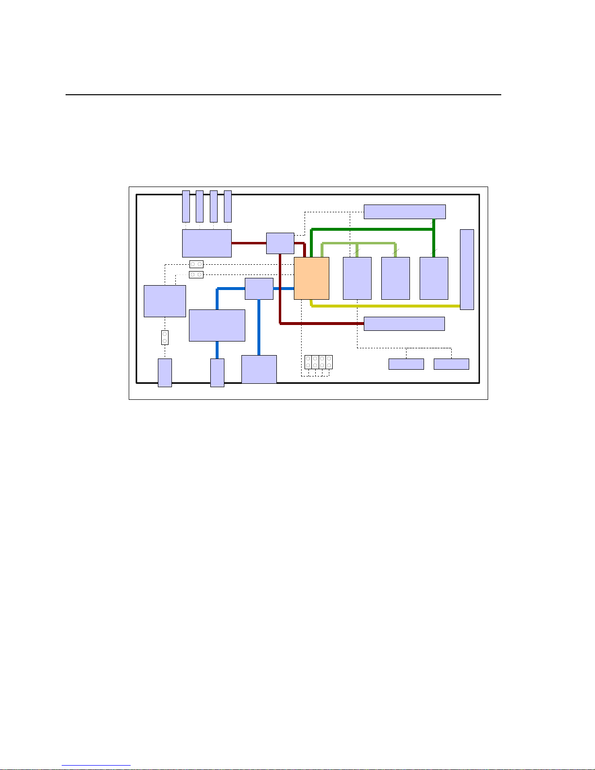
The C6416 DSK is a low-cost standalone development platform that enables users to
evaluate and develop applications for the TI C64xx DSP family. The DSK also serves
as a hardware reference design for the TMS320C6416 DSP. Schematics, logic
equations and application notes are available to ease hardware development and
reduce time to market.
Mem ory Exp
8
CPLD
Flash
Periph eral Exp
LED DIP
32
648
SDRAM
Host Port Int
0 1 2 30 1 2 3
Voltage
Reg
JP4
5V
PWR
MIC I N
LINE IN
LINE OUT
AIC23
Codec
JP1 1.4V
JP2 3.3V
JTAG
Embedded
JTAG
USB
HP OUT
McB SPs
MUX
EMIFA
EMIFB
6416
MUX
Ext.
JTAG
DSP
ENDIAN
132
HPI
BOOTM 1
BOOTM 0
PLL_SELECT
Config
SW 3
4
Figure 1-1, Block Diagram C6416 DSK
The DSK comes with a full compliment of on-board devices that suit a wide variety of
application environments. Key features include:
• A Texas Instruments TMS320C6416 DSP operating at 600 or 720 MHz.
• An AIC23 stereo codec
• 16 Mbytes of synchronous DRAM
• 512 Kbytes of non-volatile Flash memory
• 4 user accessible LEDs and DIP switches
• Software board configuration through registers implemented in CPLD
• Configurable boot options and clock input selection
• Standard expansion connectors for daughter card use
• JTAG emulation through on-board JTAG emulator with USB host
interface or external emulator
• Single voltage power supply (+5V)
1-2 TMS320C6416 DSK Module Technical Reference
Page 10

Spectrum Digital, Inc
1.2 Functional Overview of the TMS320C6416 DSK
The DSP on the 6416 DSK interfaces to on-board peripherals through one of two
busses, the 64-bit wide EMIFA and the 8-bit wide EMIFB. The SDRAM, Flash and
CPLD are each connected to one of the busses. EMIFA is also connected to the
daughtercard expansion connectors which is used for third party add-in boards.
An on-board AIC23 codec allows the DSP to transmit and receive analog signals.
McBSP1 is used for the codec control interface and McBSP2 is used for data. Analog
I/O is done through four 3.5mm audio jacks that correspond to microphone input, line
input, line output and headphone output. The codec can select the microphone or the
line input as the active input. The analog output is driven to both the line out (fixed
gain) and headphone (adjustable gain) connectors. McBSP1 and McBSP2 can be
re-routed to the expansion connectors in software.
A programmable logic device called a CPLD is used to implement glue logic that ties
the board components together. The CPLD also has a register based user interface
that lets the user configure the board by reading and writing to the CPLD registers.
The DSK includes 4 LEDs and 4 position DIP switch as a simple way to provide the
user with interactive feedback. Both are accessed by reading and writing to the CPLD
registers.
An included 5V external power supply is used to power the board. On-board switching
voltage regulators provide the 1.4V DSP core voltage and 3.3V I/O supplies. The
board is held in reset until these supplies are within operating specifications. A
separate regulator powers the 3.3V lines on the expansion interface.
Code Composer communicates with the DSK through an embedded JTAG emulator
with a USB host interface. The DSK can also be used with an external emulator
through the external JTAG connector.
1 -3
Page 11

Spectrum Digital, Inc
1.3 Basic Operation
The DSK is designed to work with TI’s Code Composer Studio development
environment and ships with a version specifically tailored to work with the board.
Code Composer communicates with the board through the on-board JTAG emulator.
To start, follow the instructions in the Quick Start Guide to install Code Composer.
This process will install all of the necessary development tools, documentation and
drivers.
After the install is complete, follow these steps to run Code Composer. The DSK must
be fully connected to launch the DSK version of Code Composer.
1) Connect the included power supply to the DSK.
2) Connect the DSK to your PC with a standard USB cable (also included).
3) Launch Code Composer from its icon on your desktop.
Detailed information about the DSK including a tutorial, examples and reference
material is available in the DSK’s help file. You can access the help file through Code
Composer’s help menu. It can also be launched directly by double-clicking on the file
c6416dsk.hlp in Code Composer’s docs\hlp subdirectory.
1-4 TMS320C6416 DSK Module Technical Reference
Page 12

Spectrum Digital, Inc
1.4 Memory Map
The C64xx family of DSPs has a large byte addressable address space. Program code
and data can be placed anywhere in the unified address space. Addresses are always
32-bits wide.
The memory map shows the address space of a generic 6416 processor on the left
with specific details of how each region is used on the right. By default, the internal
memory sits at the beginning of the address space. Portions of memory can be
remapped in software as L2 cache rather than fixed RAM.
Each EMIF (External Memory Interface) has 4 separate addressable regions called
chip enable spaces (CE0-CE3). The SDRAM occupies CE0 of EMIFA while the CPLD
and Flash are mapped to CE0 and CE1 of EMIFB respectively. Daughtercards use
CE2 and CE3 of EMIFA.
Generic 6416
Address
0x00000000
0x00100000
Address Space
Internal Memory
Reserved Space
or
Peripheral Regs
6416 DSK
Internal
Memory
Reserved
or
Peripheral
0x60000000
0x64000000
0x68000000
EMIFB CE0
EMIFB CE1
CPLD
Flash
EMIFB CE2
0x6C000000
EMIFB CE3
0x80000000
SDRAM
0x90000000
0xA0000000
EMIFA CE0
EMIFA CE1
EMIFA CE2
Daughter
0xB0000000
Card
EMIFA CE3
Figure 1-2, Memory Map, C6416 DSK
1 -5
Page 13
Spectrum Digital, Inc
1.5 Configuration Switch Settings
The DSK has 3 configuration switches that allows users to control the operational state
of the DSP when it is released from reset. The configuration switch block is labeled
SW3 on the DSK board, next to the reset switch.
Configuration switch 1 controls the endianness of the DSP while switches 2 and 3
configure the boot mode that will be used when the DSP starts executing. By default all
switches are off which corresponds to EMIFB boot (out of 8-bit Flash) in little endian
mode. The figure below shows these settings.
Table 1: Configuration Switch Settings
Switch 4 Switch 3 Switch 2 Switch 1 Configuration Description
Off 720 Mhz operation (60 Mhz
input clock)
On 600 Mhz operation (50 Mhz
input clock)
Off Off EMIF boot from 8-bit Flash
Off On No Boot
On Off Reserved
On On HPI boot
Off Little endian
On Big endian
1.6 Power Supply
The DSK operates from a single +5V external power supply connected to the main
power input (J5). Internally, the +5V input is converted into +1.4V and +3.3V using a
dual voltage regulator. The +1.4V supply is used for the DSP core while the +3.3V
supply is used for the DSP's I/O buffers and all other chips on the board. The power
connector is a 2.5mm barrel-type plug.
There are three power test points on the DSK at JP1, JP2 and JP4. All 6416 I/O
current passes through JP2 while all core current passes through JP1. All system
current passes through JP4. Normally these jumpers are closed. To measure the
current passing through remove the jumpers and connect the pins with a current
measuring device such as a multimeter or current probe.
The DSK provides +3.3V, up to 1A for the daughter card. The +3.3V supply is derived
from the +5V power source via the main +3.3 volt regulator. It is also possible to
provide the daughter card with +12V and -12V when the external power connector (J6)
is used.
1-6 TMS320C6416 DSK Module Technical Reference
Page 14

Chapter 2
Board Components
This chapter describes the operation of the major board components on
the TMS320C6416 DSK.
Topic Page
2.1 CPLD (Programmable Logic) 2-2
2.1.1 CPLD Overview 2-2
2.1.2 CPLD Registers 2-3
2.1.3 USER_REG Register 2-3
2.1.4 DC_REG Register 2-4
2.1.5 Version Register 2-4
2.1.6 MISC Register 2-5
2.2 AIC23 Codec 2-6
2.3 Sychronous DRAM 2-7
2.4 Flash Memory 2-7
2.5 LEDs and DIP Switches 2-7
2.6 Daughter Card Interface 2-8
2 -1
Page 15

Spectrum Digital, Inc
2.1 CPLD (Programmable Logic)
The C6416 DSK uses an Altera EPM3128TC100-10 Complex Programmable Logic
Device (CPLD) device to implement:
• 4 Memory-mapped control/status registers that allow software
control of various board features.
• Address decode and memory access logic.
• Control of the daughter card interface and signals.
• Assorted "glue" logic that ties the board components together.
2.1.1 CPLD Overview
The CPLD logic is used to implement functionality specific to the DSK. Your own
hardware designs will likely implement a completely different set of functions or take
advantage of the DSPs high level of integration for system design and avoid the use
of external logic completely.
The CPLD implements simple random logic functions that eliminate the need for
additional discrete devices. In particular, the CPLD aggregates the various reset
signals coming from the reset button and power supervisors and generates a global
reset.
The EPM3128TC100-10 is a 3.3V (5V tolerant), 100-pin QFP device that provides
128 macrocells, 80 I/O pins, and a 10 ns pin-to-pin delay. The device is
EEPROM-based and is in-system programmable via a dedicated JTAG interface
(a 10-pin header on the DSK). The CPLD source files are written in the industry
standard VHDL (Hardware Design Language) and included with the DSK.
2-2 TMS320C6416 DSK Module Technical Reference
Page 16
Spectrum Digital, Inc
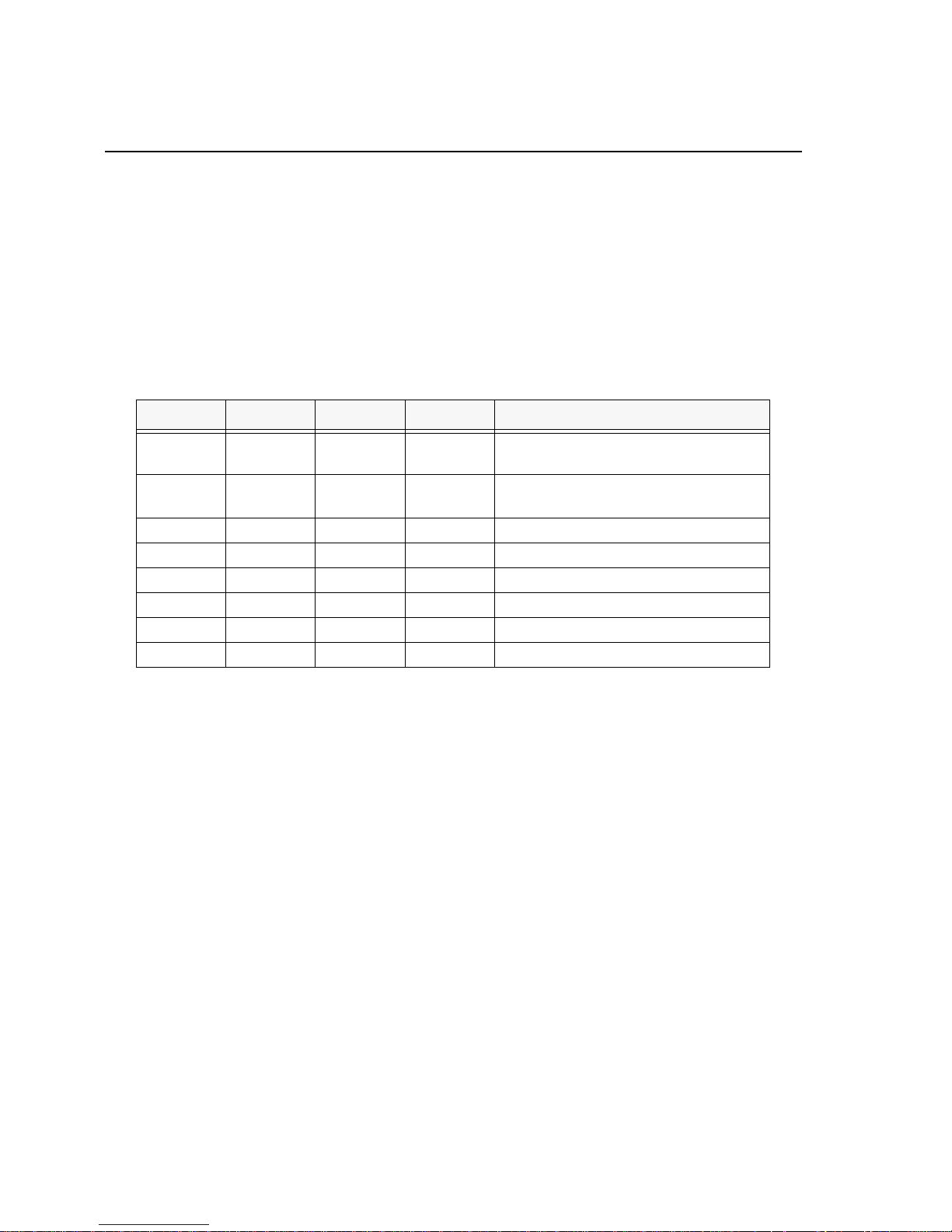
2.1.2 CPLD Registers
The 4 CPLD memory-mapped registers allows users to control CPLD functions in
software. On the 6416 DSK the registers are primarily used to access the LEDs and
DIP switches and control the daughter card interface. The registers are mapped into
EMIFB data space at address 0x60000000. They appear as 8-bit registers with a
simple asynchronous memory interface. The following table gives a high level
overview of the CPLD registers and their bit fields:
The table below shows the bit definitions for the 4 registers in CPLD.
Table 1: CPLD Register Definitions
Offset Name Bit 7 Bit 6 Bit 5 Bit 4 Bit 3 Bit 2 Bit 1 Bit 0
0USER_REGUSR_SW3RUSR_SW2RUSR_SW1
1 DC_REG DC_DET
4 VERSION CPLD_VER[3.0]
6 MISC McBSP2_EN
R
R
(MCBSP2
enabled)
0 DC_STAT1
SCR_4
R/W
0
R
R
R
SCR_3
R/W
0
USR_SW0RUSR_LED3
DC_STAT0RDC_RST
DSPPLL_
SELECT
R
1
R/W
0(Off)
R
0(No reset)
0 BOARD VERSION[2.0]
DSPPLL_
ENABLE
R
1
USR_LED2
R/W
0(Off)
0DC_CNTL1
FLASH_PAGE
R/W
0
(A19=0)
USR_LED1
R/W
0(Off)
R/W
0(low)
R
McBSP2
ON/OFF
Board
R/W
0
(Onboard)
USR_LED0
R/W
0(Off)
DC_CNTL0
R/W
0(low)
McBSP1
ON/OFF
Board
R/W
0
(Onboard)
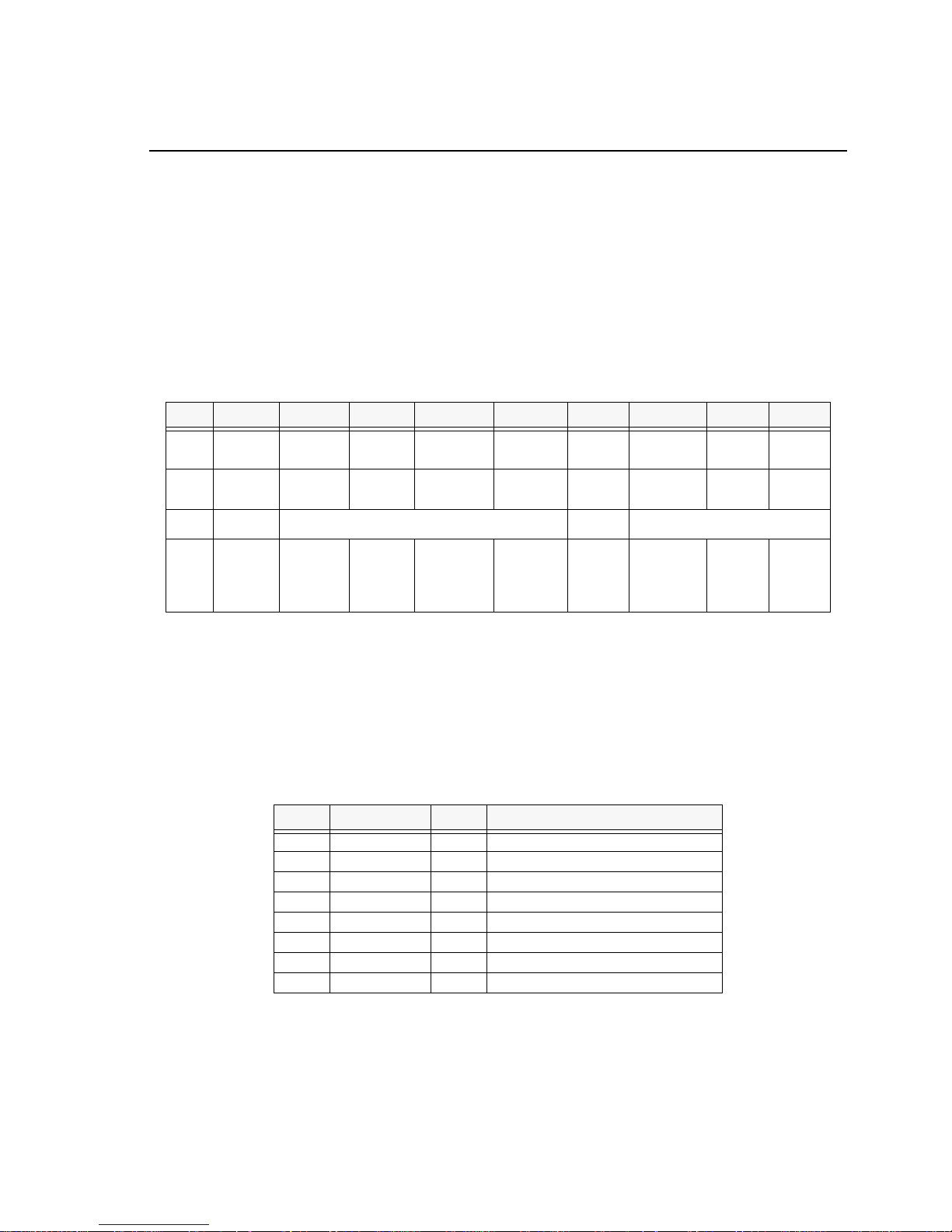
2.1.3 USER_REG Register
USER_REG is used to read the state of the 4 DIP switches and turn the 4 LEDs on or
off to allow the user to interact with the DSK. The DIP switches are read by reading the
top 4 bits of the register and the LEDs are set by writing to the low 4 bits.
Table 2: CPLD USER_REG Register
Bit Name R/W Description
7 USER_SW3 R User DIP Switch 3(1 = Off, 0 = On)
6 USER_SW2 R User DIP Switch 2(1 = Off, 0 = On)
5 USER_SW1 R User DIP Switch 1(1 = Off, 0 = On)
4 USER_SW0 R User DIP Switch 0(1 = Off, 0 = On)
3 USER_LED3 R/W User-defined LED 3 Control (0 = Off, 1 = On)
2 USER_LED2 R/W User-defined LED 2 Control (0 = Off, 1 = On)
1 USER_LED1 R/W User-defined LED 1 Control (0 = Off, 1 = On)
0 USER_LED0 R/W User-defined LED 0 Control (0 = Off, 1 = On)
2 -3
Page 17

Spectrum Digital, Inc
2.1.4 DC_REG Register
DC_REG is used to monitor and control the daughter card interface. DC_DET detects
the presence of a daughter card. DC_STAT and DC_CNTL provide simple
communications with the daughter card through readable status lines and writable
control lines.
The daughter card is released from reset when the DSP is released from reset.
DC_RST can be used to put the card back in reset.
Bit Name R/W Description
7 DC_DET R Daughter Card Detect (1= Board detected)
6 0 R Always 0
5 DC_STAT1 R Daughter Card Status 1 (0=Low, 1 = High)
4 DC_STAT0 R Daughter Card Status 0 (0=Low, 1 = High)
3 DC_RST R/W Daughter Card Reset (0=No Reset, 1 = Reset)
2 0 R Always zero
1 DC_CNTL1 R/W Daughter Card Control 1(0 = Low, 1 = High)
0 DC_CNTL0 R/W Daughter Card Control 0(0 = Low, 1 = High)
Table 3: DC_REG Register
2.1.5 VERSION Register
The VERSION register contains two read only fields that indicate the BOARD and
CPLD versions. This register will allow your software to differentiate between
production releases of the DSK and account for any variances. This register is not
expected to change often, if at all.
Bit # Name R/W Description
7 CPLD_VER3 R Most Significant CPLD Version Bit
6 CPLD_VER2 R CPLD Version Bit
5 CPLD_VER1 R CPLD Version Bit
4 CPLD_VER0 R Least Significant CPLD Version Bit
3 0 R Always 0
2 DSK_VER2 R Most Significant DSK Board Version Bit
1 DSK_VER1 R DSK Board Version Bit
0 DSK_VER0 R Least Significant DSK Board Version Bit
Table 4: Version Register Bit Definitions
2-4 TMS320C6416 DSK Module Technical Reference
Page 18

Spectrum Digital, Inc
2.1.6 MISC Register
The MISC register is used to provide software control for miscellaneous board
functions. On the 6416 DSK, the MISC register controls how auxiliary signals are
brought out to the daughter-card connectors.
McBSP1 and McBSP2 are usually used as the control and data ports of the on-board
AIC23 codec. The power-on state of these bits (both 0s) represents that configuration.
Set MCBSP1SEL or MCBSP2SEL to route the McBSPs to the daughtercard
connectors rather than the codec.
The Flash and CPLD share CE1 which means that the highest address bit (A21) is
used to differentiate between the two. In this configuration 512Kbytes of 8-bit Flash are
visible at the beginning of CE1 which matches the chip on the production board. If the
Flash is replaced with a 1Mbyte chip, only 512Kbytes of Flash will still be visible but
FLASH_PAGE can be used to select between the top and bottom halves.
FLASH_PAGE replaces the address bit (A21) that is lost sharing CE1 with the CPLD.
An on-board PLL is used to generate the DSP’s input clock frequency. The
DSPPLL_SELECT and DSPPLL_ENABLE bits are read-only versions of the PLL
configuration signals. DSPPLL_ENABLE will read 1 if the PLL is enabled.
DSPPLL_SELECT (set by configuration switch #4) switches between a 50 Mhz and
60 Mhz input clock.
The 6416’s PCI interface and McBSP2 share some pins. The McBSP2_EN signal is
used to disable McBSP2 when the PCI interface is active. McBSP2_EN is generated
on the board when an appropriate daughtercard that uses PCI is plugged in, it can be
read through this CPLD bit.
The scratch bits are unused. They can be set to any value.
Table 5: MISC Register
Bit Name R/W Description
7 McBSP2_EN R Value of McBSP2_EN from PCI header
6 SCRATCH_4 R/W Scratch bit 4
5 SCRATCH_3 R/W Scratch bit 3
4 DSPPLL_SELECT R PLL select (0 = 50/600 Mhz, 1 = 60/720 Mhz)
3 DSPPLL_ENABLE R PLL enable (0 = off, 1 = on)
2 FLASH_PAGE R/W Flash address bit 19
1 MCBSP2SEL R/W McBSP2 on/off board (0 = on-board, 1 = off-board)
0 MCBSP1SEL R/W McBSP1 on/off board (0 = on-board, 1 = off-board)
2 -5
Page 19

Spectrum Digital, Inc
2.2 AIC23 Codec
The DSK uses a Texas Instruments AIC23 (part #TLV320AIC23) stereo codec for input
and output of audio signals. The codec samples analog signals on the microphone or
line inputs and converts them into digital data so it can be processed by the DSP.
When the DSP is finished with the data it uses the codec to convert the samples back
into analog signals on the line and headphone outputs so the user can hear the output.
The codec communicates using two serial channels, one to control the codec’s internal
configuration registers and one to send and receive digital audio samples. McBSP1 is
used as the unidirectional control channel. It should be programmed to send a 16-bit
control word to the AIC23 in SPI format. The top 7 bits of the control word should
specify the register to be modified and the lower 9 should contain the register value.
The control channel is only used when configuring the codec, it is generally idle when
audio data is being transmitted,
McBSP2 is used as the bi-directional data channel. All audio data flows through the
data channel. Many data formats are supported based on the three variables of
sample width, clock signal source and serial data format. The DSK examples generally
use a 16-bit sample width with the codec in master mode so it generates the frame
sync and bit clocks at the correct sample rate without effort on the DSP side. The
preferred serial format is DSP mode which is designed specifically to operate with the
McBSP ports on TI DSPs.
The codec has a 12MHz system clock. The 12MHz system clock corresponds to USB
sample rate mode, named because many USB systems use a 12MHz clock and can
use the same clock for both the codec and USB controller. The internal sample rate
generate subdivides the 12MHz clock to generate common frequencies such as
48KHz, 44.1KHz and 8KHz. The sample rate is set by the codec’s SAMPLERATE
register. The figure below shows the codec interface on the C6416 DSK.
AIC23 Codec
0 LEFTINVOL
1 RIGHT INVO L
FSX1
CLKX1
TX1
DR2
FSX2
CLKR
CLKX
FSR2
DX2
McBSP1
SPI Format
Digital
McBSP2
DSP Format
SCLK
SDIN
DOUT
LRCOUT
BCLK
LRCIN
DIN
CS
2 LEFTHPV O L
3 RIGHTHPVOL
4 ANAPATH
5 DIGPATH
6 POWERDOWN
7 DIGIF
Control Registers
8 SAMPLERATE
9 DIGACT
15 RESET
ADC
DAC
Analog
MIC I N
LINE IN
LINE OUT
HP O UT
MIC I N
LINE IN
LINE OUT
HP O UT
Figure 2-1, TMS320C6416 DSK CODEC INTERFACE
2-6 TMS320C6416 DSK Module Technical Reference
Page 20

Spectrum Digital, Inc
2.3 Synchronous DRAM
The DSK uses a pair of industry standard 64 megabit SDRAMs in CE0 of EMIFA. The
two devices are used in parallel to create a 64-bit wide interface. Total available
memory is 16 megabytes.
The DSK uses an EMIFA clock of 120 MHz. The integrated SDRAM controller is
started by configuring the EMIF in software. Timings can be found in the SDRAM
datasheet and the DSK help file. When using the SDRAM, note that one row of the
memory array must be refreshed at least every 15.6 microseconds to maintain the
integrity of its contents.
2.4 Flash Memory
The DSK uses a 512Kbyte external Flash as a boot option. It is connected to CE1 of
EMIFB with an 8-bit interface. Flash is a type of memory which does not lose its
contents when the power is turned off. When read it looks like a simple asynchronous
read-only memory (ROM). Flash can be erased in large blocks commonly referred to
as sectors or pages. Once a block has been erased each word can be programmed
once through a special command sequence. After than the entire block must be erased
again to change the contents.
The Flash requires 70ns for both reads and writes. The general settings used with the
DSK use 8 cycles for both read and write strobes (80ns) to leave a little extra margin.
2.5 LEDs and DIP Switches
The DSK includes 4 software accessible LEDs (D7-D10) and DIP switches (SW1) that
provide the user a simple form of input/output. Both are accessed through the CPLD
USER_REG register.
2 -7
Page 21

Spectrum Digital, Inc
2.6 Daughter Card Interface
The DSK provides three expansion connectors that can be used to accept plug-in
daughter cards. The daughter card allows users to build on their DSK platform to
extend its capabilities and provide customer and application specific I/O. The
expansion connectors are for memory, peripherals, and the Host Port Interface (HPI)
The memory connector provides access to the DSP’s asynchronous EMIF signals to
interface with memories and memory mapped devices. It supports byte addressing on
32 bit boundries. The peripheral connector brings out the DSP’s peripheral signals like
McBSPs, timers, and clocks. Both connectors provide power and ground to the
daughter card
The HPI is a high speed interface that can be used to allow multiple DSPs to
communicate and cooperate on a given task. The HPI connector brings out the HPI
specific control signals as well as McBSP2.
Most of the expansion connector signals are buffered so that the daughter card cannot
directly influence the operation of the DSK board. The use of TI low voltage, 5V tolerant
buffers, and CBT interface devices allows the use of either +5V or +3.3V devices to be
used on the daughter card.
Other than the buffering, most daughter card signals are not modified on the board.
However, a few daughter card specific control signals like DC_RESET and
DC_DET exist and are accessible through the CPLD DC_REG register. The DSK
also multiplexes the McBSP1 and McBSP2 of on-board or external use. This function
is controlled through the CPLD MISC register.
2-8 TMS320C6416 DSK Module Technical Reference
Page 22

Chapter 3
Physical Description
This chapter describes the physical layout of the TMS320C6416 DSK
and its connectors.
Topic Page
3.1 Board Layout 3-2
3.2 Connector Index 3-3
3.3 Expansion Connectors 3-3
3.3.1 J4, Memory Expansion Connector 3-4
3.3.2 J3, Peripheral Expansion Connector 3-5
3.3.3 J1, HPI Expansion Connector 3-6
3.4 Audio Connectors 3-7
3.4.1 J301, Microphone Connector 3-7
3.4.2 J303, Audio Line In Connector 3-7
3.4.3 J304, Audio Line Out Connector 3-8
3.4.4 J302, Headphone Connector 3-8
3.5 Power Connectors 3-9
3.5.1 J5, +5 Volt Connector 3-9
3.5.2 J6, Optional Power Connector 3-9
3.6 Miscellaneous Connectors 3-10
3.6.1 J201, USB Connector 3-10
3.6.2 J8, External JTAG Connector 3-10
3.6.3 JP3, PLD Programming Connector 3-11
3.7 System LEDs 3-11
3.8 Reset Switch 3-12
3 -1
Page 23

Spectrum Digital, Inc
3.1 Board Layout
The C6416 DSK is a 8.75 x 4.5 inch (210 x 115 mm.) multi-layer board which is
powered by an external +5 volt only power supply. Figure 3-1 shows the layout of the
C6416 DSK.
J6
J5
J201
J301
J303
Figure 3-1, TMS320C6416 DSK
JP3
J304
J302
SW1
J3
D7-10
J4
SW2
J1 J2
J8
3-2 TMS320C6416 DSK Module Technical Reference
Page 24

Spectrum Digital, Inc
3.2 Connector Index
The TMS320C6416 DSK has many connectors which provide the user access
to the various signals on the DSK.
Table 1: TMS320C6416 DSK Connectors
Connector # Pins Function
J4 80 Memory
J3 80 Peripheral
J1 80 HPI
J301 3 Microphone
J303 3 Line In
J304 3 Line Out
J303 3 Headphone
J5 2 +5 Volt
J6 * 4 Optional Power Connector
J8 14 External JTAG
J201 5 USB Port
JP3 10 CPLD Programming
SW3 8 DSP Configuration Jumper
Note: “*” Not populated
3.3 Expansion Connectors
The TMS320C6416 DSK supports three expansion connectors that follow the Texas
Instruments interconnection guidelines. The expansion connector pinouts are
described in the following three sections.
The three expansion connectors are all 80 pin 0.050 x 0.050 inches low profile
connectors from Samtec or AMP. The Samtec SFM Series (surface mount) connectors
are designed for high speed interconnections because they have low propagation
delay, capacitance, and cross talk. The connectors present a small foot print on the
DSK. Each connector includes multiple ground, +5V, and +3.3V power signals so that
the daughter card can obtain power directly from the DSK. The peripheral expansion
connector additionally provides both +12V and -12V to the daughter card. The
recommended mating connector, whose part number is TFM-140-32-S-D-LC, is a
surface mount connector that provides a 0.465” mated height.
Note: I is on an Input pin
O is on an Output pin
Z is on a High Impedance pin
3 -3
Page 25

Spectrum Digital, Inc
3.3.1 J4, Memory Expansion Connector
Table 2: J4, Memory Expansion Connector
Pin Signal I/O Description Pin Signal I/O Description
1 5V Vcc 5V voltage supply pin 2 5V Vcc 5V voltage supply pin
3 AEA21 O EMIF address pin 21 4 AEA20 O EMIF address pin 20
5 AEA19 O EMIF address pin 19 6 AEA18 O EMIF address pin 18
7 AEA17 O EMIF address pin 17 8 AEA16 O EMIF address pin 16
9 AEA15 O EMIF address pin 15 10 AEA14 O EMIF address pin 14
11 GND Vss System ground 12 GND Vss System ground
13 AEA13 O EMIF address pin 13 14 AEA12 O EMIF address pin 12
15 AEA11 O EMIF address pin 11 16 AEA10 O EMIF address pin 10
17 AEA9 O EMIF address pin 9 18 AEA8 O EMIF address pin 8
19 AEA7 O EMIF address pin 7 20 AEA6 O EMIF address pin 6
21 5V Vcc 5V voltage supply pin 22 5V Vcc 5V voltage supply pin
23 AEA5 O EMIF address pin 5 24 AEA4 O EMIF address pin 4
25 AEA3 O EMIF address pin 3 26 AEA2 O EMIF address pin 2
27 ABE3# O EMIF byte enable 3 28 ABE2# O EMIF byte enable 2
29 ABE1# O EMIF byte enable 1 30 ABE0# O EMIF byte enable 0
31 GND Vss System ground 32 GND Vss System ground
33 AED31 I/O EMIF data pin 31 34 AED30 I/O EMIF data pin 30
35 AED29 I/O EMIF data pin 29 36 AED28 I/O EMIF data pin 28
37 AED27 I/O EMIF data pin 27 38 AED26 I/O EMIF data pin 26
39 AED25 I/O EMIF data pin 25 40 AED24 I/O EMIF data pin 24
41 3.3V Vcc 3.3V voltage supply pin 42 3.3V Vcc 3.3V voltage supply pin
43 AED23 I/O EMIF data pin 23 44 AED22 I/O EMIF data pin 22
45 AED21 I/O EMIF data pin 21 46 AED20 I/O EMIF data pin 20
47 AED19 I/O EMIF data pin 19 48 AED18 I/O EMIF data pin 18
49 AED17 I/O EMIF data pin 17 50 AED16 I/O EMIF data pin 16
51 GND Vss System ground 52 GND Vss System ground
53 AED15 I/O EMIF data pin 15 54 AED14 I/O EMIF data pin 14
55 AED13 I/O EMIF data pin 13 56 AED12 I/O EMIF data pin 12
57 AED11 I/O EMIF data pin 11 58 AED10 I/O EMIF data pin 10
59 AED9 I/O EMIF data pin 9 60 AED8 I/O EMIF data pin 8
61 GND Vss System ground 62 GND Vss System ground
63 AED7 I/O EMIF data pin 7 64 AED6 I/O EMIF data pin 6
65 AED5 I/O EMIF data pin 5 66 AED4 I/O EMIF data pin 4
67 AED3 I/O EMIF data pin 3 68 AED2 I/O EMIF data pin 2
69 AED1 I/O EMIF data pin 1 70 AED0 I/O EMIF data pin 0
71 GND Vss System ground 72 GND Vss System ground
73 AARE# O EMIF async read enable 74 AAWE# O EMIF async write enable
75 AAOE# O EMIF async output enable 76 AARDY I EMIF asynchronous ready
77 ACE3# O Chip enable 3 78 ACE2# O Chip enable 2
79 GND Vss System ground 80 GND Vss System ground
3-4 TMS320C6416 DSK Module Technical Reference
Page 26

Spectrum Digital, Inc
3.3.2 J3, Peripheral Expansion Connector
Table 3: J3, Peripheral Expansion Connector
Pin Signal I/O Description Pin Signal I/O Description
1 12V Vcc 12V voltage supply pin 2 -12V Vcc -12V voltage supply pin
3 GND Vss System ground 4 GND Vss System ground
5 5V Vcc 5V voltage supply pin 6 5V Vcc 5V voltage supply pin
7 GND Vss System ground 8 GND Vss System ground
9 5V Vcc 5V voltage supply pin 10 5V Vcc 5V voltage supply pin
11 N/C - No connect 12 N/C - No connect
13 N/C - No connect 14 N/C - No connect
15 N/C - No connect 16 N/C - No connect
17 N/C - No connect 18 N/C - No connect
19 3.3V Vcc 3.3V voltage supply pin 20 3.3V Vcc 3.3V voltage supply pin
21 CLKX0 I/O McBSP0 transmit clock 22 CLKS0 I McBSP0 clock source
23 FSX0 I/O McBSP0 transmit frame sync 24 DX0 O McBSP0 transmit data
25 GND Vss System ground 26 GND Vss System ground
27 CLKR0 I/O McBSP0 receive clock 28 N/C - No connect
29 FSR0 I/O McBSP0 receive frame sync 30 DR0 I McBSP0 receive data
31 GND Vss System ground 32 GND Vss System ground
33 CLKX2 I/O McBSP2 transmit clock 34 CLKS2 I McBSP2 clock source
35 FSX2 I/O McBSP2 transmit frame sync 36 DX2 O McBSP2 transmit data
37 GND Vss System ground 38 GND Vss System ground
39 CLKR2 I/O McBSP2 receive clock 40 N/C - No connect
41 FSR2 I/O McBSP2 receive frame sync 42 DR2 I McBSP2 receive data
43 GND Vss System ground 44 GND Vss System ground
45 TOUT0 O Timer 0 output 46 TINP0 I Timer 0 input
47 N/C - No connect 48 EXT_INT5 I External interrupt 5
49 TOUT1 O Timer 1 output 50 TINP1 I Timer 1 input
51 GND Vss System ground 52 GND Vss System ground
53 EXT_INT4 I External interrupt 4 54 N/C - No connect
55 N/C - No connect 56 N/C - No connect
57 N/C - No connect 58 N/C - No connect
59 RESET O System reset 60 N/C - No connect
61 GND Vss System ground 62 GND Vss System ground
63 CNTL1 O Daughtercard control 1 64 CNTL0 O Daughtercard control
65 STAT1 I Daughtercard status 1 66 STAT0 I Daughtercard status
67 EXT_INT6 I External interrupt 6 68 EXT_INT7 I External interrupt 7
69 ACE3# O Chip enable 3 70 N/C - No connect
71 N/C - No connect 72 N/C - No connect
73 N/C - No connect 74 N/C - No connect
75 DC_DET# Vss System ground 76 GND Vss System ground
77 GND Vss System ground 78 ECL KOUT O EMIF Clock
79 GND Vss System ground 80 GND Vss System ground
3 -5
Page 27

Spectrum Digital, Inc
3.3.3 J1, HPI Expansion Connector
Table 4: J1, HPI Expansion Connector
Pin Signal I/O Description Pin Signal I/O Description
1 PCI_EN I PCI enable 2 BSP2_EN I MCBSP2_EN
3 GND Vss System ground 4 HPI_RS# I HPI reset
5 XSP_CS O PCI serial 6 BEA13 I PCI EEPROM auto-init
7 GND Vss System ground 8 GND Vss System ground
9 AD1 I/O PCI address/data 1 10 PCBE0# I/O PCI command/byte ena 0
11 AD3 I/O PCI address/data 3 12 AD0 I/O PCI address/data 0
13 AD5 I/O PCI address/data 5 14 AD2 I/O PCI address/data 2
15 AD7 I/O PCI address/data 7 16 AD4 I/O PCI address/data 4
17 GND System ground 18 AD6 I/O PCI address/data 6
19 AD8 I/O PCI address/data 8 20 GND Vss System ground
21 AD10 I/O PCI address/data 10 22 AD9 I/O PCI address/data 9
23 AD12 I/O PCI address/data 12 24 AD11 I/O PCI address/data 11
25 AD14 I/O PCI address/data 14 26 AD13 I/O PCI address/data 13
27 GND Vss System ground 28 AD15 I/O PCI address/data 15
29 PCBE1# I/O PCI command/byte ena 1 30 GND Vss System ground
31 GND Vss System ground 32 PPAR I/O PCI parity
33 PSERR# I/O PCI system error 34 GND Vss System ground
35 GND Vss System ground 36 PSTOP# I/O PCI stop
37 PPERR# I/O PCI parity error 38 GND Vss System ground
39 GND Vss System ground 40 PTRDY# I/O PCI target ready
41 PDEVSEL# I/O PCI device select 42 GND Vss System ground
43 GND Vss System ground 44 PFRAME# I/O PCI Frame
45 PIRDY# I/O PCI initiator ready 46 GND Vss System ground
47 GND Vss System ground 48 AD16 I/O PCI address/data 16
49 PCBE2# I/O PCI command/byte ena 2 50 AD18 I/O PCI address/data 18
51 AD17 I/O PCI address/data 17 52 AD20 I/O PCI address/data 20
53 AD19 I/O PCI address/data 19 54 AD22 I/O PCI address/data 22
55 AD21 I/O PCI address/data 21 56 GND Vss System ground
57 AD23 I/O PCI address/data 23 58 PIDSEL I PCI init device select
59 PCBE3# I/O PCI command/byte ena 3 60 AD24 I/O PCI address/data 24
61 GND Vss System ground 62 AD26 I/O PCI address/data 26
63 AD25 I/O PCI address/data 25 64 AD28 I/O PCI address/data 28
65 AD27 I/O PCI address/data 27 66 AD30 I/O PCI address/data 30
67 AD29 I/O PCI address/data 29 68 PGNT# I PCI bus grant
69 AD31 I/O PCI address/data 31 70 GND Vss System ground
71 GND Vss System ground 72 PRST# I PCI reset
73 PREQ# O PCI bus request 74 GND Vss System ground
75 GND Vss System ground 76 PINTA# O PCI interrupt A
77 PCLK I PCI Clock 78 GND Vss System ground
79 GND Vss System ground 80 N/C - No connect
3-6 TMS320C6416 DSK Module Technical Reference
Page 28

Spectrum Digital, Inc
3.4 Audio Connectors
The C6416 DSK has 4 audio connectors. They are described in the following
sections.
3.4.1 J301, Microphone Connector
The input is a 3.5 mm. stereo jack. Both inputs are connected to the microphone so it is
monaural. The signals on the plug are shown in the figure below.
Ground
Microphone In
Microphone Bias
Figure 3-2, Microphone Stereo Jack
3.4.2 J303, Audio Line In Connector
The audio line in is a stereo input. The input connector is a 3.5 mm stereo jack. The
signals on the mating plug are shown in the figure below.
Ground
Right Line In
Left Line In
Figure 3-3, Audio Line In Stereo Jack
3 -7
Page 29

Spectrum Digital, Inc
3.4.3 J304, Audio Line Out Connector
The audio line out is a stereo output. The output connector is a 3.5 mm stereo jack. The
signals on the mating plug are shown in the figure below.
Figure 3-4, Audio Line Out Stereo Jack
3.4.4 J303, Headphone Connector
Connector J4 is a headphone/speaker jack. It can drive standard headphones or a high
impedance speaker directly. The standard 3.5 mm jack is shown in the figure below
.
Ground
Right Line Out
Left Line Out
Ground
Right Headphone
Left Headphone
Figure 3-5, Headphone Jack
3-8 TMS320C6416 DSK Module Technical Reference
Page 30

Spectrum Digital, Inc
3.5 Power Connectors
The C6416 DSK has 2 power connectors. They are described in the following
sections.
3.5.1 J5, +5 Volt Connector
Power (+5 volts) is brought onto the TMS320C6416 DSK via connector J5. The
connector has an outside diameter of 5.5 mm. and an inside diameter of 2.5 mm. The
A diagram of J5 is shown below.
+5V
J5
Front View
Figure 3-6, TMS320C6416 DSK Power Connector
3.5.2 J6, Optional Power Connector
Ground
PC Board
Connector J6 is an optional power connector. It will operate with the standard personal
computer power supply. To populate this connector use a Molex #15-24-4041. The
table below shows the voltages on the respective pins.
Table 5: J6, Optional Power Connector
Pin # Voltage Level
1 +12 Volts
2-12 Volts
3 Ground
4+5 Volts
WARNING !
Do not plug into J5 and J6 at the same time.
3 -9
Page 31

Spectrum Digital, Inc
3.6 Miscellaneous Connectors
The C6416 DSK has 3 additional connectors to aid the user in developing with this
product. They are described in the following sections.
3.6.1 J201, USB Connector
Connector J201 provides a Universal Serial Bus (USB) Interface to the embedded
JTAG emulation logic on the DSK. This allows for code development and debug
without the use of an external emulator. The signals on this connector are shown in the
below.
Table 6: J201, USB Connector
Pin # USB Signal Name
1 USBVdd
2D+
3D-
4 USB Vss
5 Shield
6 Shield
3.6.2 J8, External JTAG Connector
The TMS320C6416 DSK is supplied with a 14 pin header interface, J8. This is the
standard interface used by JTAG emulators to interface to Texas Instruments DSPs.
The pinout for the connector is shown figure 3-6 below.
TMS
TDI
PD (+3.3V)
TDO
TCK-RET
TCK
EMU0
1
34
5
7
9
11
13
TRST-
2
Header Dimensions
Pin-to-Pin spacing, 0.100 in. (X,Y)
Pin width, 0.025-in. square post
Pin length, 0.235-in. nominal
6
8
10
12
14
GND
no pin (key)
GND
GND
GND
EMU1
Figure 3-7, JTAG INTERFACE
3-10 TMS320C6416 DSK Module Technical Reference
Page 32

Spectrum Digital, Inc
The signal names for each pin are shown in the table below.
Table 7: J8, JTAG Interface
Pin # Signal Name
1TMS
2TRST-
3TDI
4GND
5PD
6 no pin
7TDO
8GND
9TCK-RET
10 GND
11 TCK
12 GND
13 EMU0
14 EMU1
3.6.3 JP3, PLD Programming Connector
This connector interfaces to the Altera CPLD, U12. It is used in the in the factory for the
programming of the CPLD. This connector is not intended to be used outside the
factor y.
3.7 System LEDs
TheTMS320C6416 DSK has four system light emitting diodes (LEDs). These
LEDs indicate various conditions on the DSK. These function of each LED is shown in
the table below.
Table 8: System LEDs
Reference
Designator
D4 Green USB Emulation in use. When External JTAG
D3 Green +5 Volt present 1
D6 Orange RESET Active 1
DS201 Green USB Active, Blinks during USB data transfer 1
Color Function
Emulator is used this LED is off.
On Signal
State
1
3-1 1
Page 33

Spectrum Digital, Inc
3.8 Reset Switch
There are three resets on the TMS320C6416 DSK. The first reset is the power on
reset. This circuit waits until power is within the specified range before releasing the
power on reset pin to the TMS320C6416.
External sources which control the reset are push button SW2, and the on board
embedded USB JTAG emulator.
3-12 TMS320C6416 DSK Module Technical Reference
Page 34

Appendix A
Schematics
This appendix contains the schematics for the TMS320C6416 DSK.
Board components with designators between 200 and 299 (e.g. DS201,
R211) are part of Spectrum Digital’s embedded JTAG emulator and are not
included in these schematics.
A -1
Page 35

Spectrum Digital, Inc
AA
SPECT R U M DIGI T A L INCORPORATED
of
114Friday, August 15, 2003
505942ETMS320C6416 DSK
B
Title
Size Document Number Rev
Date: Sheet
The TMS320C6416 DSK design is based on
TMS320C6416 device device data sheet
DATE
SPRS146E and errata SPRZ011H. This
schematic is subject to change without
notification. Spectrum Digital Inc. assumes no
liability for applications assistance, customer
product design or infringement of patents
described herein.
DATE
DATE
DATE
DATE
DATE
DATE
13-August-2003
QA
ENGR - MGR
DW N
ENGR
CHK
REVI SI ON STATUS OF SHEETS
REV
A-2 TMS320C6416 DSK Module Technical Reference
RLS E
MFG
USED ON
APPLICATION
NEXT ASSY
1234567
8 9 10 11 12 13 14
EEEBEAE
DCDBBAA
REV
SH
SH
SH
REV
Page 36

Spectrum Digital, Inc
D10
R82
150
3.3V
1K
DGND
1K
1K
GREEN
D9
R81
150
GREEN
of
214Friday, August 15, 2003
R56 10K
R35 10K
R23 10K
R40 10K
R98 10K
R97 10K
USB_DSP_RST#
DC_EMIFA_OE#
CPLD_MCBSP1_MUX
CPLD_MCBSP2_MUX
DC_STAT0
DC_STAT1
SN74AHC1G14
4
U8
5
2
MMBD4148
D11
1 3
R84
3.3V
C119
10K
R83
33
4
RESET
SW2
PUSHBUTTON
1
2 3
DGND
R22
DSP_RST#
3
0.1uF
R39
R24
PULLUP/DOWN TO KEEP LOGIC IN RESET
BRD_RST#
3.3V
DGND
GND
D
WHEN THE CPLD IS NOT PROGRAMMED.
FLASH_PAGE
DC_STAT0
DC_STAT1
25967581523754793169833276845780
U12
DC_STAT0
DC_STAT1
VCCIO
82
VCCIO
66
VCCIO
51
VCCIO
34
VCCIO
18
VCCIO
3
VCCINT
91
VCCINT
39
DSP_DQ0
DSP_DQ1
426441634445465840
TBED1
TBED0
TBED[7..0]
(4)
3.3V
DC_CNTL0
DC_CNTL1
DC_EMIFA_OE#
DC_EMIFA_DIR
DC_CNTL_OE#
DC_RST#
C_RESETn
DC_CNTL0
DC_CNTL1
D
DC_DBUF_DIR
DC_CNTL_OEn
DC_DBUF_OEn
DSP_DQ2
DSP_DQ3
DSP_DQ4
DSP_DQ5
DSP_DQ6
DSP_DQ7
DSP_ADDR0
13
BED3TBED2
TBED7
TBED6
TBED5
TBED4
T
TBEA1
TBEA2
TBEA[3..1](4)
RN19D10K
RN19E10K
RN19F10K
RN19G10K
SW1
3.3V
DC_DET
DC_DETn
SP_ADDR1
D
100
TBEA3
5
4
DSP_ADDR2
CPLD_MCBSP1_MUX
MCBSP_SEL0
R80
R79
R78
CPLD_MCBSP2_MUX
MCBSP_SEL1
DSP_CSn
989019
D8
150
GREEN
D7
150
GREEN
D6
YELLOW
150
USER_LED1
USER_LED0
USER_LED3
USER_LED2
TP10
TP
TP16TPTP19TPTP20TPTP15
MCBSP2_EN
BRD_RST#
DSP_RST#
FLASH_PAGE
716847
67
603048
21
165661
SPARE0
SPARE1
SPARE2
DSP_RSn
BRD_RSn
MCBSP2_EN
DSP_WEn
DSP_REn
DSP_OEn
178510
TBCE0#(4)
TBAOE#(4)
TBARE#(4)
TBAWE#(4)
876
SW DIP-4/SM
123
DGND
USER_LED3
FLASH_PAGE
DSP_RSn_LED
CPLD_CLK_OUT
DSP_DC_CS0n
DSP_DC_CS1n
DSP_DC_WEn
DSP_DC_REn
DSP_DC_OEn
USER_SW3
8
9
12
1435939497
TACE3#(3,9)
TACE2#(3,9)
TASDWE#(3,9)
TASDCAS#(3,9)
TASDRAS#(3,9)
R33
R34
3.3V
R53
PADDLE SWITCH
SPARE3
USER_LED0
USER_LED1
USER_LED2
CLKIN
EMU_RSTn
USER_SW0
USER_SW1
USER_SW2
PWB_REV0
PWB_REV1
PWB_REV2
202329
876369299
CODEC_CLK
PWB_REV2
PWB_REV1
PWB_REV0
R36
NU
1K
NU
1K
R37
NU
R54
1K
Advisory 1 .1. XX
REV E PWB
P
T
CLKMODE0
CLKMODE1
RSV0
CLKMODE0
PONRSn
PUSHBRSn
GND
CLKMODE1
GND
GND
GND
GND
GND
GND
GND
GND
GND
GND
GND
GND
GND
HPIRSn
TCK
TMS
TDI
TDO
62
15473
SR_TCK
I
ISR_TMS
ISR_TDI
ISR_TDO
DGND
SVS_RST#(12)
PUSHB_RS
HPI_RESET#
USB_DSP_RST#
CPLD
DSPPLL_S0
DSPPLL_S1
DSPPLL_SELECT
DSPPLL_ENABLE
EPM3128ATC100-10
95
89
88
86
78
74
65
59
53
43
38
33
26
11
DGND
3.3V
12345678910
JP3
3.3V
505942ETMS320C6416 DSK
B
Title
Size Document Number Rev
Date: Sheet
C40
0.1
DGND
C70
0.1
C39
0.1
C72
0.1
C71
0.1
C69
0.1
C68
0.1
C38
0.1
RN19A10K
RN19C10K
RN19B10K
HEADER 5X2
DGND
A -3
Page 37

Spectrum Digital, Inc
4X
5.33X5X2.5X2X3.33X6X3X
0-BC, 1-AB, OPEN-M
OPTIONAL ON REV D PWB AND
HIGHER
S1 S0 MULTIPLIER
00M001
M0
MM
M1
8X
10
1M
11
JP401
JPSMT
C
A
1
3
B
DGND
3.3V
U10E
AC7
2
2
JP400
JPSMT
C
A
1
3
B
C400
NU
X2
S1
20MHz
Y1
U400
X1/CLK
VDD
123
DGND DGND
C401
NU
3.3V
DSP_EMU11(2)
DSP_EMU10(2)
DSP_TDO (13)
TP27TP29
TP5
TP6
TP8
TP7
AE19
AD18
AC18
D6B5A4
AF6
AE6
AD6
AC6
GP00
GP01_CLKOUT4
XTINT4_GP04
NMI
E
EXTINT5_GP05
RESET
B4
AF5
AE5
AD5
TDO
GP03
EMU10
TOUT0
TOUT1
TOUT2
GP02_CLKOUT6
EXTINT6_GP06
EXTINT7_GP07
TINP0
TINP1
TINP2
TDI
TMS
C6A5C5
AF4
AF18
AF16
AB16
33 OHM, A TO B
WHEN USED, B TO C
WHEN NOT USED.
JP402
JPSMT
A
C
1
3
B
DGND
2
678
S0
ICS512
GND
REF CLK
4 5
PLACE COMPONENTS ON BACKSIDE
OF PWB AS CLOSE TO U10 PIN H25
AS POSSIBLE.
3-PIN SMT JUMPERS ACCEPT 603
DGND
C402
.01UF
DSP_EMU0 (2)
DSP_EMU1 (2)
DSP_EMU4 (2)
DSP_EMU6 (2)
DSP_EMU5 (2)
DSP_EMU2 (2)
DSP_EMU3 (2)
AF15
AC15
AE16
AD16
AC16
AE17
AD17
EMU0
EMU1
EMU2
EMU3
EMU4
EMU5
EMU11
TCLK
TRST
CLKMODE0
CLKMODE1
PLLV
J6
H2
G1
AB15
RESISTORS.
DSP_EMU9 (2)
DSP_EMU8 (2)
DSP_EMU7 (2)
AF17
AC17
AE18
20 MHz
EMU6
H4
AECLKIN
EMU7
EMU8
EMU9
MULTIPLIER
0-BC, 1-AB, OPEN-M
REV E PWB AND HIGHER
S0110
TMS320C6416GLZ
AECLKIN
BECLKIN
CLKIN
Advisory 1.03.01
A11
H25
600 MHz
480 MHz
4X
5.33X5X2.5X2X3.33X6X3X
M
0
00S1
M
0
M
1
of
314Friday, August 15, 2003
505942ETMS320C6416 DSK
B
Title
Size Document Number Rev
Date: Sheet
720 MHz
8X
1
1
10MMM
TP28
DSP_RST#
DSP_TDI(13)
DSP_TMS(13)
DSP_TCK(13)
DSP_TRST#(13)
DGND
C121
0.1
EINT4
EINT5
EINT6
EINT7
TINP0
TINP1
TOUT0
TOUT1
256910
24
Vcc
1B1
XDS_4.1V
1A1
U21
347
C_EINT4
D
10)
(
1516192023
1B2
1B3
1B4
1B5
2B1
1OE
1A2
1A3
1A4
1A5
2A1
1
8
11
1417182122
DC_EINT6(10)
DC_EINT7(10)
DC_TINP0(10)
DC_EINT5(10)
DC_TINP1(10)
DGND
12
2B2
2B3
2B4
2B5
GND
Plac e all PLL external components as close
to th e DSP. All PLL external components
must be on a single side of the board.
Maximize the distance between switching signals
and the PLL external components.
2OE
2A2
2A3
2A4
2A5
SN74CBTD3384PW
13
R77
DC_TOUT0(10)
DC_TOUT1(10)
R51 NU
360
DGND
EMI FILTER
IO
E1
EXCCET103U
1 3
DSPIO_3.3 V
C92
0.1
CT10
10
+
DGND
GND
2
CLKMODE0
CLKMODE1
CLKMODE[1:0]: Core CLKIN multiples
00 = x1
R30
NU
R29
1K
3.3V
CLKMODE0
CLKMODE1
NO-POP
MUST DRIVE 1/0/Z, Z FOR
U500
3.3V
OPEN
DGND
X2
X1/CLK
123
L5
DSP_CORE_CLK
AB ENABLE DSPPLL_S0/S1
DRIVE FROM CPLD
BC USE JP500/JP501 TO
R50 33
DSPPLL_S0
DSPPLL_S1
3.3V
678
S0
S1
ICS512
VDD
GND
REF CLK
4 5
C113
0.01
C114
0.1
Ferrite Chip
SET FREQUENCY
JP502
JPSMT
A
C
1
3
B
DGND
2
DSPPLL_ENABLE
DGND
OPTIONAL
R17
C22
NO-POP
DGND
JP501
JPSMT
A
C
1
3
B
3.3V
01 = x6
10 = x12 (Default)
11 = Reserved
R27
1K
R28
NU
2
2
JP500
JPSMT
C
A
1
3
B
C501
6pF NPO
20MHz
Y500
DGND DGND
6pF NPO
C500
DGND
A-4 TMS320C6416 DSK Module Technical Reference
Page 38

Spectrum Digital, Inc
(9)
(9)
9)
(
ABE3#
TASDRAS# (2,9)
TASDWE# (2,9)
TASDCAS# (2,9)
TACE2# (2,9)
TABE2# (9)
T
TACE3# (2,9)
TABE1# (9)
TAEA[22..3]
TAED[63..0]
TABE0# (9)
NEAR SDRAM
RN3H33
RN3G33
TAED63
TAED62
RN3F33
TAED61
RN3E33
TAED60
RN3D33
RN3C33
TAED59
TAED58
RN3B33
TAED57
RN3A33
RN4H33
TAED56
TAED55
RN4G33
RN4F33
TAED54
TAED53
RN4E33
RN4D33
TAED52
RN4C33
TAED51
TAED50
RN4B33
RN4A33
TAED49
RN5H33
TAED48
TAED47
RN5G33
RN5F33
TAED46
RN5E33
TAED45
RN5D33
TAED44
RN5C33
TAED43
TAED42
RN5B33
TAED41
RN5A33
RN6H33
TAED40
RN6G33
TAED39
TAED38
RN6F33
RN6E33
TAED37
TAED36
RN6D33
RN6C33
TAED35
RN6B33
TAED34
RN6A33
TAED33
TAED32
U9
U13
AED63
AED62
AED61
AED60
AED59
AED58
AED57
AED56
AED55
AED54
AED53
AED52
AED51
AED50
AED49
AED48
AED47
AED46
AED45
AED44
AED43
AED42
AED41
AED40
AED39
AED38
AED37
AED36
AED35
AED34
AED33
AED32
TAEA16
TAEA14
TAEA15
23
22
21
BA1
BA0
DQ0
DQ1
24578
AED34
T
TAED33
TAED32
TAED0
TAED2
TAED1
24578
DQ0
DQ1
BA1
BA0
23
22
21
TAEA14
TAEA15
TAEA16
23
TAEA13
24666564636261602726
NC
DQ2
TAED35
TAED3
DQ2
NC
24666564636261602726
TAEA13
AF24
AF23
AE23
AE22
AD22
AF22
AD21
AE21
AC21
AF21
AD20
AE20
AC20
AF20
AC19
AD19
W24
W23
Y26
Y
Y25
Y24
AA26
AA23
AA25
AA24
AB26
AB24
AB25
AC25
AC26
AD26
U10A
TAEA5
TAEA11
TAEA9
TAEA6
TAEA4
TAEA7
TAEA10
TAEA12TAED4
A9A8A7A6A5A4A3A2A1
A10
DQ3
DQ4
DQ5DQ6
10111374767779808283853134363739404245474850515354
AED36
TAED37
T
TAED39
TAED38
TAED7
TAED5
TAED6
10111374767779808283853134363739404245474850515354
DQ3
DQ4
DQ5DQ6
A10A9A8A7A6A5A4A3A2A1A0
AEA12
T
TAEA11
TAEA10
TAEA9
NEAR DSP
AED63
AED62
AED61
AED60
AED59
AED58
AED57
AED56
AED55
AED54
AED53
AED52
AED51
AED50
AED49
AED48
AED47
AED46
AED45
AED44
AED43
AED42
AED41
AED40
AED39
AED38
AED37
AED36
AED35
AED34
AED33
AED32
NEAR DSP
TABE7#
TAEA8
DQ7
TAED40
TAED8
DQ7
TAEA8
TABE7#
RN7A33
ABE7#
T23
T22
AEA22
RN8A33
TAEA22
TABE6#
TAEA3
8
25
59
2
A0
DQM3
DQ8
DQ9
DQ10
DQ11
DQ12
DQ13
DQ14
DQ15
TAED48
TAED45
TAED42
TAED46
TAED43
TAED44
TAED47
TAED41
AED15
TAED14
T
TAED10
TAED16
TAED12
TAED11
TAED9
TAED13
DQ8
DQ9
DQ10
DQ11
DQ12
DQ13
DQ14
DQ15
DQM3
8
25
59
2
TAEA3
TAEA4
TAEA5
TAEA6
TAEA7
ABE3#
TABE2#
T
3.3V
TABE3#
TABE2#
TABE6#
TABE0#
TABE5#
TABE4#
TABE1#
N7C
RN7B33
RN7H33
RN7G33
RN7F33
RN7E33
RN7D33
R
3
3
ABE1#
ABE6#
ABE5#
ABE0#
ABE2#
ABE4#
ABE3#
T24
R25
R26
M25
M26
L23
L24
ABE7
ABE6
ABE5
ABE4
ABE3
ABE2
ABE1
ABE0
AEA22
AEA21
AEA20
AEA19
AEA18
AEA17
AEA16
AEA15
V24
V25
V26
T25T26
U23
U24
U25
U26
EA20
EA19
A
AEA14
AEA17
AEA15
AEA18
AEA21
A
AEA16
N8C
RN8H33
RN8G33
RN8F33
RN8E33
RN8D33
R
RN8B33
RN9A33
3
3
AEA20
AEA19
TAEA21
TAEA17
T
T
TAEA18
TAEA16
TAEA15
TAEA14
TABE5#
71
DQM2
DQ16
33
TAED49
TAED17
33
DQ16
DQM2
71
TABE1#
R41
TACE3#
R46 33
ACE3#
L26
AEA14
AEA13
RN9B33
TAEA13
TACE0#
TABE4#
16
735730
QM0
DQM1
D
Q17
DQ18
DQ19
D
TAED51
TAED50
TAED52
TAED19
TAED18
TAED20
Q17
DQ18
DQ19
D
QM0
DQM1
D
16
735730
TABE0#
TACE2#
TACE0#
R44 33
R43 33
TP17
ACE2#
ACE0#
K23
K24
K25
CE2
ACE3
A
ACE1
TMS320C6416GLZ
EA13
A
AEA12
AEA11
P23
R23
R24
AEA12
AEA11
AEA10
RN9E33
RN9D33
RN9C33
TAEA10
TAEA11
TAEA12
NCNCNC
DQ20
DQ21
TAED54
TAED53
TAED22
TAED21
DQ20
DQ21
NCNCNC
10K
ACE0
AEA10
AEA9
P24
AEA8
AEA9
RN9G33
RN9F33
TAEA9
TAEA8
TASDWE#
TASDRAS#
TASDCAS#
68
CS
DQ25
TAED58
TAED26
DQ25
CS
TASDRAS#
AHOLDA
AEA5
AEA4
RN12C33
TAEA4
191817
RAS
DQ26
TAED59
TAED27
DQ26
RAS
191817
TASDCAS#
TASDCAS#
R47 33
TP12
ASDCAS#
R22
ASOE3
AEA4
M23
AEA3
RN12D33
TAEA3
67
8672584484785246383212
70
69
NC
NC
WE
VSS
VSS
VSS
CLK
CAS
CKE
VDD
VDD
DQ30
DQ31
56
TAED63
TAED31
56
DQ30
DQ31
CLK
CKE
NC
NC
68
67
70
69
TAECLKOUT1 TAECLKOUT1
TASDCKE TASDCKE
TAEA17 TAEA17
TAECLKOUT2 (9)
TAECLKOUT1
TASDCKE
R42 33
R26 33
R49 33
ASDCKE
AECLKOUT2
AECLKOUT1
L25
J26
J23
ASDCKE
AECLKOUT1
AECLKOUT2
AARDY
AHOLD
L22
V23
AARDY
TP14
R25 33
TAARDY
VDD
43291518175554941
43291518175554941359
VDD
VDD
VDD
VSS
VSS
VSS
8672584484785246383212
AED31
AED30
AED29
AED28
AED27
AED26
AED25
AED24
AED23
AED22
AED21
AED20
AED19
AED18
AED17
AED16
AED15
AED14
AED13
AED12
AED11
AED10
AED9
AED8
AED7
AED6
AED5
AED4
AED3
AED2
AED1
AED0
DQ27
DQ28
DQ29
TAED61
TAED62
TAED60
TAED28
TAED29
TAED30
DQ27
DQ28
DQ29
CAS
WE
TASDWE#
TASDRAS#
TASDWE#
R45 33
R48 33
ASDWE#
ASDRAS#
J25
J24
K26
A_AWE/SDWE/SWE
A_AOE/SDRAS/SOE
A_ARE/SDCAS/SADS/SRE
AEA3
M24
6
VSS
VSSQ
VSSQ
VSSQ
VSSQ
VSSQ
VSSQ
VSSQ
VSSQ
VDD
VDDQ
VDDQ
VDDQ
VDDQ
VDDQ
VDDQ
VDDQ
VDDQ
9
3
35
3.3V
3
VDD
VDDQ
VDDQ
VDDQ
VDDQ
VDDQ
VDDQ
VDDQ
VDDQ
VSS
VSSQ
VSSQ
VSSQ
VSSQ
VSSQ
VSSQ
VSSQ
VSSQ
6
C26
AED31
D26
AED30
D25
AED29
E25
AED28
E24
AED27
E26
AED26
F24
AED25
F25
AED24
F23
AED23
F26
AED22
G24
AED21
G25
AED19
G23
AED20
G26
AED18
H23
AED17
H24
AED16
C19
AED15
D19
AED14
A
20
AED13
D20
AED12
B20
AED11
C20
AED10
A21
AED9
D21
AED8
B21
AED7
C21
AED6
A22
AED5
C22
AED4
B22
AED3
B23
AED2
A23
AED1
A24
AED0
20
14
NC
DQ22
DQ23
DQ24
TAED57
TAED56
TAED55
TAED25
TAED23
TAED24
DQ22
DQ23
DQ24
NC
20
14
TACE0#
TP18
TP11
TP13
M22
P22
N22
APDT
ABUSREQ0
AEA8
AEA7
AEA6
P26
N23
N24
N26
AEA5
AEA7
AEA6
RN12B33
RN12A33
RN9H33
TAEA7
TAEA6
TAEA5
C45
0.1
3.3V
MT48LC2M32B2TG-6
MT48LC2M32B2TG-6
DGND DGND
NEAR SDRAM
RN13A33
RN13B33
RN13C33
RN13D33
RN13E33
RN13F33
RN13G33
RN13H33
RN10H33
RN10G33
RN10F33
RN10E33
RN10D33
RN10C33
RN10B33
RN10A33
RN14A33
RN14B33
RN14C33
RN14D33
RN14E33
RN14F33
RN14G33
RN14H33
RN11H33
RN11G33
RN11F33
RN11E33
RN11D33
RN11C33
RN11B33
RN11A33
DGND
C74
0.1
C42
0.1
C44
0.1
C97
0.1
C95
0.1
C75
0.1
EMIFA & SDRAM
C73
0.1
C43
0.1
C41
0.1
10
CT5
+
10
CT13
+
TAED31
TAED30
TAED29
TAED28
TAED27
TAED26
TAED25
TAED24
TAED23
TAED22
TAED21
TAED20
TAED19
TAED18
TAED17
TAED16
TAED15
TAED14
TAED13
TAED12
TAED11
TAED10
TAED9
TAED8
TAED7
TAED6
TAED5
TAED4
TAED3
TAED2
TAED1
TAED0
505942BTMS320C6416 DSK
B
Title
Size Document Number Rev
of
414Friday, August 15, 2003
Date: Sheet
A -5
TAARDY(9)
Page 39

Spectrum Digital, Inc
of
TBEA[3..1] (2)
TBED[7..0] (2)
514Friday, August 15, 2003
3.3V
SW3
OFF - OPEN
ON - CLOSED
ENDIAN
BOOT-1
BOOT-0
.3V
3
R504
NU
R75
1K
R72
1K
R71
NU
R70
1K
R69
NU
R68
1K
R85 1K
IPU
876
123
GND
DSPPLL_SELECT
D
TBCE0# (2)
TBARE# (2)
R87 1K
R503 1K
R86 1K
5
SW DIP-4/SM
PENCIL SWITCH
4
DGND
TBEA11
TBEA13
IPU
IPD
TBAOE#(2)
R505
1K
R74
NU
R73
NU
C93
0.1
2)
(
BAWE#
T
DGND
DGND
3.3V
U10B
E16
TBED3
TBED1
TBED0
TBED4
TBED2
293133353840424430323436394143
DQ0
DQ1
DQ2
DQ3
A0 VCC
U15
25 37
TBEA7
TBEA5
TBEA8
TBEA4
TBEA2
TBEA3
NEAR DSP
A13
C12
D13
C13
BBE1
BBE0
BCE3
TMS320C6416GLZ
BEA20
BEA19
BEA18
BEA17
BEA16
BEA15
BEA14
BEA13
BEA12
A18
A17
B18
B17
D18
C18
D17
C17
D16
DQ4
BCE2
BEA11
TBED5
TBEA9
R63 33
BCE1# TBCE1#
TBED6
TBED7
DQ5
DQ6
A7A6A5A4A3A2A1
8
18192021222324
TBEA10
TBEA11
R59 33
BCE0# TBCE0 #
B12
A12
BCE1
BCE0
BEA10
BEA9
A16
B16
C16
TBEA1
101314
15
4517
DQ7
DQ8
DQ9
DQ10
DQ11
DQ12
DQ13
DQ14
RY/BY
DQ15/A-1A17
A14
A15
A16
A13
A12
A11
A10A9A8
TBEA14
TBEA13
TBEA12
TP26
TP24
E12
E14
E13
BPDT
BBUSREQ0
BEA8
BEA7
BEA6
B15
D15
C15
A19
A18
2
14834567
9
16
BEA16
TBEA17
TBEA15TBEA4
TBEA18
TBEA20
T
TBEA19
10K
FLASH_PAGE
R57
3.3V
TP30
TP23
TBAOE#
TBECLKOUT1
TBAWE#BAWE#
TBECLKOUT2
TBARE#
R58 33
R61 33
R60 33
R62 33
R64 33
TP25
TP22
BECLKOUT2
BECLKOUT1
BARE#
BAOE#
E15
A10
B11
C11
D12
D11
BSOE3
BHOLDA
BEA5
BECLKOUT1
B_AWE/SDWE/SWE
B_AOE/SDRAS/SOE
B_ARE/SDCAS/SADS/SRE
BEA4
BEA3
BEA2
BEA1
BARDY
BHOLD
A15
A14
E11
B19
D14
C14
DGND
46
27
VSS
VSS
NC1
NC2
NC3
EMIFB & FLASH
OEWERESET
BYTE
CE
AM29LV400B
2628111247
DGND
BAWE#
TBAOE#
T
TBCE1#
BRD_RST#
BED15
BECLKOUT2
D7
BED14
B6
BED13
C7
BED12
A6
BED11
D8
BED10
B7
BED9
C8
BED8
A7
BED7
C9
BED6
B
8
BED5
D9
BED4
B9
BED3
C10
BED2
A9
BED1
D10
BED0
B10
NEAR DSP
RN18H33
BED7
RN18G33
BED6
RN18F33
BED5
RN18E33
BED4
RN18D33
BED3
RN18C33
BED2
BED1
RN18B33
BED0
RN18A33
505942ETMS320C6416 DSK
B
Title
Size Document Number Rev
Date: Sheet
TBED7
TBED6
TBED5
TBED4
TBED3
TBED2
TBED1
TBED0
LIL_ENDIAN
BOOT_MODE1
BOOT_MODE0
AECLKIN_SEL1
AECLKIN_SEL0
BECLKIN_SEL0
BECLKIN_SEL1
EEAI
UTOPIA_EN
TBEA20
TBEA19
TBEA11
TBEA18
TBEA17
TBEA15
TBEA14
TBEA16
TBEA13
TBEA8
TBEA9
A-6 TMS320C6416 DSK Module Technical Reference
BEA13
RN15H33
TBEA13 TBEA6
BEA6
BEA7
BEA11
BEA8
BEA3
BEA10
BEA9
BEA12
RN16C33
RN16B33
RN16A33
TBEA12
TBEA11
TBEA10
BEA2
BEA5
BEA4
BEA1
TP21
RN17D33
RN17C33
RN17B33
RN17A33
RN16H33
RN16G33
RN16F33
RN16E33
RN16D33
TBEA9
TBEA1
TBEA3
TBEA8
TBEA7
TBEA5
TBEA2
TBEA6
BEA17
BEA19
BEA20
BEA14
BEA15
BEA18
BEA16
RN15G33
RN15F33
RN15E33
RN15D33
RN15C33
RN15B33
RN15A33
NEAR DSP
TBEA14
TBEA15
TBEA20
TBEA16
TBEA17
TBEA19
TBEA18
Page 40

Spectrum Digital, Inc
DC_DR0 (10)
DC_CLKX0 (10)
DC_CLKR0 (10)
DC_CLKS0 (10)
DC_DX0 (1 0)
DC_FSR0 (10)
0.1
C120
DGND
256910
24
DS_4.1V
X
Vcc
1B1
1A1
U20
347
CLKS0
F4D1E1D2E2C1E3
CLKS0
1B2
1B3
1A2
1A3
CLKX0
CLKR0
CLKX0
CLKR0
DC_FSX0 (10)
1516192023
1B4
1B5
2B1
2B2
2B3
2B4
2B5
GND
1OE
1A4
1A5
1
8
11
DX0
DR0
FSR0
DX0
DR0
FSR0
2A1
1417182122
FSX0
FSX0
2OE
2A2
2A3
2A4
2A5
SN74CBTD3384PW
13
R76
360
DGND
MCBSP
DGND
12
505942ATMS320C6416 DSK
B
Title
Size Document Number Rev
of
614Friday, August 15, 2003
Date: Sheet
3.3V
4147119
1A
1B2
2B1
356
DC_FSR2(10)
DC_DX2(10)
AIC23SDATAIN
MCBSP2_EN
R55
1K
1213
3A
4B12A3B1
3B2
2B2
10
DC_FSX2(10)
LRCIN
LRCOUT
DGND
8
4A4B2
GND
S
OE
SN74CBT3257PW
1
15
R12
360
DGND
CPLD_MCBSP2_MUX
U10D
CLKS2_GP08
CLKR2
CLKX2_XSPCLK
AE4
AB1
AC2
DR2
CLKS2
CLKR2
0.1
C13
DCISO-4.1V
LM4040DCIM3-4.1
D1
2 1
R1
1.6K
5V
U4
DGND
CLKX2
DGND
4147119
16
1213
1A
3A
VCC
2
4A4B2
4B12A3B1
1B1
3B2
1B2
2B1
2B2
356
10
DC_CLKS2(10)
DC_CLKR2(10)
DC_CLKX2(10)
DC_DR2(10)
BCLK
TMS320C6416GLZ
DR2_XSPDI
DX2_XSPDO
FSR2
FSX2
MCBSP2_EN
AA2
AF3
AB3
AB2
AC1
DX2
FSX2
FSR2
8
16
VCC
GND
S
OE
1B1
SN74CBT3257PW
U3
1
AIC23SDATAOUT
2
15
A -7
Page 41

Spectrum Digital, Inc
PDEVSELn
PSTOPn
PTRDYn
PCBE2n
PSERRn
PCBE1n
R3T4R1
AD31_HD31
J2
PAD31
PAD30
PAD29
PAD28
PAD27
PAD26
PAD25
PAD24
PAD23
PAD22
PAD21
PAD20
PAD19
PAD18
PAD17
PAD16
PAD15
PAD14
PAD13
PAD12
PAD11
PAD10
PAD9
PAD8
PAD7
PAD6
PAD5
PAD4
PAD3
PAD2
PAD1
PAD0
AD30_HD30
K3
AD29_HD29
J1
AD28_HD28
K4
AD27_HD27
K2
AD26_HD26
L3
AD25_HD25
K1
AD24_HD24
L4
AD23_HD23
L1
AD22_HD22
M4
AD21_HD21
M2
AD20_HD20
N4
AD19_HD19
M1
AD18_HD18
N5
AD17_HD17
N1
AD16_HD16
P5
AD15_HD15
U4
AD14_HD14
U1
AD13_HD13
U3
AD12_HD12
U2
AD11_HD11
V4
AD10_HD10
V1
AD9_HD9
V3
AD8_HD8
V2
AD7_HD7
W2
AD6_HD6
W4
AD5_HD5
Y1
AD4_HD4
Y3
AD3_HD3
Y2
AD2_HD2
Y4
AD1_HD1
AA1
AD0_HD0
AA3
PCBE2_HR/W
PSERR_HDS1
PTRDY_HHWIL
PSTOP_HCNTL0
PDEVSEL_HCNTL1
PGNT_GP12
PINTA_GP13
PCLK_GP14
PRST_GP15
PFRAME_HINT
PIRDY_HRDY
J3
P4
PIRDYn
F1
R4
G4F2G3
CLK
PFRAMEn
PRSTn
P
PINTAn
PGNTn
PREQn
of
PPERRn
PPAR
PCI_EN
AA4
T3R2T2T1P1
PCI_EN
HPI DAUGHTER CARD CAN RESET
DSP VIA THIS SIGNAL. SIGNAL IS
COMBINED WITH OTHER DSP
PPAR_HAS
PPERR_HCS
PCBE1_HDS2
RESET SOURCES.
3.3V
HPI_RESET#
R19
10K
714Friday, August 15, 2003
505942ETMS320C6416 DSK
MCBSP2_EN
TBEA13
PAD0
PAD2
PAD4
PAD6
PAD9
PAD11
PAD13
PAD15
PPAR
PSTOPn
PTRDYn
PCBE0n
12
34
56
78
910
11 12
13 14
15 16
17 18
19 20
21 22
23 24
J1
1 2
3 4
5 6
7 8
9 10
PCI_EN
XSP_CS
PCBE0
XSP_CS
PIDSEL_GP9
PCBE3_GP10
PREQ_GP11
L2
M3
PCBE3n
PIDSEL
U10C
TMS320C6416GLZ
W3
AD1
XSP_CS
PCBE0n
PAD1
25 26
11 12
13 14
15 16
17 18
19 20
21 22
23 24
25 26
27 28
PAD3
PAD5
PAD7
PAD8
PAD12
PAD14
PAD10
PAD8/PAD10 WERE
SWAPPED ON REV A/B
PWB.
PFRAMEn
27 28
29 30
31 32
33 34
35 36
37 38
39 40
41 42
29 30
31 32
33 34
35 36
37 38
39 40
41 42
43 44
PCBE1n
PSERRn
PDEVSELn
PPERRn
AD24
PAD16
PAD18
PAD20
PAD22
PIDSEL
P
PAD26
PAD28
PAD30
PGNTn
PRSTn
43 44
45 46
47 48
49 50
51 52
53 54
55 56
57 58
59 60
61 62
63 64
65 66
67 68
69 70
45 46
47 48
49 50
51 52
53 54
55 56
PIRDYn
PCBE2n
PAD19
PAD21
PAD17
71 72
57 58
59 60
61 62
63 64
65 66
67 68
69 70
71 72
73 74
PAD23
PCBE3n
PAD25
PAD29
PAD31
PREQn
PAD27
UTOPIA & HOST PORT I/F
PINTAn
73 74
75 76
77 78
79 80
SFM140L2SDLC
75 76
77 78
79 80
DGND DGND
PCLK
B
Title
Size Document Number Rev
Date: Sheet
URENB#
UXDATA5
UXDATA3
UXDATA1
UXDATA7
UXCLAV
UXCLK
37 38
39 40
41 42
43 44
45 46
47 48
39 40
41 42
43 44
45 46
47 48
49 50
RCLK
U
UXENB#
UXDATA2
UXDATA0
UXDATA2
UXDATA6
UXDATA5
UXDATA4
UXDATA3
UXDATA7
AF7
AF9
AE8
AD8
AD9
AD10
UXDATA1
UXDATA2
UXDATA3
UXDATA4
UXDATA5
UXDATA6
URDATA1
URDATA2
URDATA3
URDATA4
URDATA5
URDATA6
AF13
AF12
AE12
AE11
AC12
AC11
URDATA4
URDATA5
URDATA3
URDATA2
URDATA6
URDATA7
UXADDR1
UXADDR3
49 50
51 52
53 54
55 56
57 58
59 60
61 62
63 64
65 66
67 68
69 70
71 72
73 74
75 76
77 78
79 80
51 52
53 54
55 56
57 58
59 60
61 62
63 64
65 66
67 68
69 70
UXDATA4
UXDATA6
UXSOC
UXADDR0
UXADDR2
UXADDR4
UXCLK
UXCLAV
UXSOC
UXENB#
AD11
AC14
AE15
AC13
UXCLK
UXENB
UXSOC
UXCLAV
UXDATA7
URDATA7
URCLK
URCLAV
URENB
URSOC
TMS320C6416GLZ
AF14
AB14
AD12
AD15
URSOC
URCLAV
URCLK
URENB#
SFM-140-L2-S-D-LC
71 72
73 74
75 76
77 78
79 80
DGND DGND
A
1
B
2
JP503
SOLDER_JUMPER
TBEA11
REMOVE HARDWIRE
OF TBEA11 ON REV E
PWB
LOCATE NEAR UTOPIA HEADER/DSP
URSOC
URDATA0
URDATA6
URDATA2
13 14
URADDR0
15 16
URADDR1
URDATA4
15 16
17 18
19 20
21 22
23 24
25 26
27 28
29 30
31 32
33 34
17 18
19 20
U10F
35 36
21 22
23 24
25 26
27 28
29 30
31 32
33 34
35 36
37 38
URDATA1
URDATA5
URDATA7
URDATA3
URCLAV
DX1
UXADDR2
FSX1
UXDATA0
UXADDR1
UXADDR0
UXDATA1
AE9
AF11
AC9
AB13
AB11
AD7
AE7
UXDATA0
UXADDR0
UXADDR4_DX1
UXADDR1_DR1
UXADDR3_FSX1
UXADDR2_FSR1
URADDR0
URADDR1
URADDR2_CLKR1
URADDR3_CLKS1
URADDR4_CLKX1
URDATA0
AC8
AF10
AE10
AB12
AC10
AD13
AD14
CLKX1
URDATA0
URADDR0
URDATA1
URADDR3
URADDR1
URADDR2
URADDR2
URADDR4
CTL_FSX1
CTL_DX1
CTL_CLKX1
CPLD_MCBSP1_MUX
12
34
56
78
910
11 12
R18
360
UXADDR4
UXADDR3
URADDR4
1215
1035
6
S
OE
3B2
1B2
2B1
2B2
1B1
4B12A3B1
VCC
1A
U1
4147119
16
DX1
FSX1
C28
LM4040DCIM3-4.1
D2
R3
1.6K
5V
GND
3A
4A 4B2
8
12 13
CLKX1
.1
0
DGND
2 1
GND
D
DGND
SN74CBT3257PW
DGND
J2
1 2
3 4
5 6
7 8
9 10
11 12
UTOPIA Interface
13 14
URADDR3
A-8 TMS320C6416 DSK Module Technical Reference
Page 42

Spectrum Digital, Inc
14
C
0.1
3.3V
DC_D[31..0] (10)
DC_A[21..2] (10)
DGND
16
C
0.1
15
C
0.1
17
C
0.1
C18
0.1
3.3V
C21
0.1
C19
0.1
C20
0.1
C96
0.1
3.3V
DGND
C94
0.1
C115
0.1
C116
0.1
C117
0.1
3.3V
DGND
DGND
C99
0.1
C98
0.1
C118
0.1
#OE DIR OPERATION
L L A <-- B
L H A --> B
H X ISOLATION
DC_ECLKOUT (10)
505942CTMS320C6416 DSK
DC_BE2# (10)
DC_BE3# (10)
DC_BE0# (10)
DC_CE3# (10)
DC_AOE# (10)
DC_ARE# (10)
DC_BE1# (10)
DC_CE2# (10)
3.3V
TAARDY (3)
DC_AWE# (10)
R15 22
R403
1K
DAUGHTERCARD BUFFERING
B
Title
Size Document Number Rev
of
814Friday, August 15, 2003
Date: Sheet
3.3V
3.3V
U5
7
1831
Vcc
424746444341403837
R13
10K
3.3V
424746444341403837
Vcc
Vcc
Vcc Vcc
U17
7
18 31
DC_A17
DC_A15
DC_A16
23568911
cc
V
1B1
1B2
VccVcc
1A1
1A2
TAEA17
TAEA18
TAEA16
DC_D2
DC_D0
DC_D1
DC_D3
1A1
1A2
1A3
1B1
1B2
1B3
23568
TAED0
TAED2
TAED3
TAED1
DC_A14
1B3
1B4
1A3
1A4
AEA15
T
C_D4
D
1A4
1A5
1B4
1B5
TAED4
C_A13
DC_A10
DC_A11
DC_A12
D
12
1B5
1B6
1B7
1A5
1A6
1A7
AEA14
AEA13
TAEA11
TAEA12
T
T
C_D5
DC_D7
D
DC_D6
DC_D15
3635333230292726
1A6
1A7
1A8
1B6
1B7
1B8
9
11
12
1314161719202223
AED5
T
TAED6
TAED7
TAED15
DC_A9
131416
1B8
1A8
363533
TAEA10
DC_D14
2A1
2B1
TAED14
DC_A4
DC_A3
DC_A5
DC_A6
DC_A7
DC_A8
DC_A2TAEA3
17192022
23
2B1
2B2
2B3
2B4
2B5
2B6
2B7
2B8
2A1
2A2
2A3
2A4
2A5
2A6
2A7
2A8
1OE
1DIR
32302927
TAEA7
TAEA8
TAEA9
DC_D13
DC_D12
DC_D11
2A2
2A3
2A4
2A52A6
2B2
2B3
2B4
2B5
TAED12
TAED13
TAED11
2OE
26
48125
244101521
TAEA5
TAEA6
TAEA4
DC_D9
DC_D8
DC_D10
48125244
2A7
2A8
1OE
2OE
1DIR
2DIR
2B6
2B7
2B8
TAED8
TAED10
TAED9
2DIR
28
28343945
GND
GND
1015
GND
GND
GND
GND
3439
DGND
GND
GNDGND
3.3V
GND
GNDGND
SN74LVTH16245A
DGND
DGND
21
ND
GND
G
3.3V
GNDGND
SN74LVTH16245A
45
DGND
DC_A21
DC_A18
DC_A19
DC_A20
7
1831
23568911
Vcc
VccVcc
1B1
1B2
1B3
1B4
Vcc
1A1
1A2
1A3
U6
U16
1A4
424746444341403837
TAEA19
TAEA20
TAEA22
TAEA21
DC_D18
DC_D17
DC_D19
DC_D16
424746444341403837
Vcc
1A1
1A2
1A3
1A4
Vcc
Vcc Vcc
1B1
1B2
1B3
1B4
7
23568
18 31
TAED16
TAED18
TAED17
TAED19
1B5
1A5
TABE3#(3)
C_D20
D
1A5
1B5
TAED20
1B6
1B7
1A6
1A7
TABE2#(3)
TABE1#(3)
DC_D22
DC_D21
1A6
1A7
1B6
1B7
9
11
TAED21
TAED22
12
13141617192022
1B8
2B1
2B2
2B3
1A8
2A1
2A2
2A3
36353332302927
TABE0#(3)
TACE3#(2,3)
TACE2#(2,3)
TASDCAS#(2,3)
DC_D29
DC_D31
DC_D23
DC_D30
36353332302927
1A8
2A1
2A2
2A3
1B8
2B1
2B2
2B3
12
13141617192022
TAED23
TAED31
TAED30
TAED29
23
2B4
2B5
2B6
2B7
2B8
2A4
2A5
2A6
2A7
2A8
1OE
1DIR
2OE
26
48125
244101521
DC_ARDY(10)
TASDWE#(2,3)
TASDRAS#(2,3)
TAECLKOUT2(3)
R14
1K
C_D24
DC_D27
DC_D28
D
DC_D25
DC_D26
26
481252441015
2A4
2A5
2A6
2A7
2A8
1OE
2OE
1DIR
2B4
2B5
2B6
2B7
2B8
23
TAED24
TAED28
TAED27
TAED26
TAED25
DGNDDGND
283439
45
GND
GND
GND
GND
2DIR
GND
GND
GND
GND
SN74LVTH16245A
DGND
DGND
21
2DIR
GND
GND
GND
GND
GND
GND
GND
GND
SN74LVTH16245A
283439
45
DC_EMIFA_DIR = 0 FOR WRITES
DGND
TAEA[22..3](3)
TAED[63..0](3)
A -9
DC_CNTL_OE#
DC_EMIFA_DIR
DC_EMIFA_OE#
(2)
(2)
Page 43

Spectrum Digital, Inc
of
914Friday, August 15, 2003
DC_BE3# (9)
.3V
3
DC_A17
DC_A19
DC_A21
DC_A13
DC_A15
12345678910
1112
1314
12345678910
1112
1314
J4
External Memory InterfaceExternal Peripheral Interface
DC_A18
DC_A12
DC_A14
DC_A16
5V 5V
DC_A[21..2](9)
DC_D[31..0](9)
DC_A20
.3V
3
DC_BE1# (9)
C_A9
C_A11
D
DC_A7
D
1516
1718
1920
2122
1516
1718
1920
C_A10
D
DC_A6
DC_A8
DC_D27
DC_A3
DC_D29
DC_D25
DC_D31
7
2324
2526
2
2930
3132
3334
3536
3738
3940
4142
9
2122
2324
2526
2728
2
3132
3334
3536
3738
3940
0
3
8
2
DC_A2
DC_A4 DC_A5
DC_D30
DC_D24
DC_D26
DC_D28
DC_BE0#(9)
DC_BE2#(9)
DC_D11
DC_D19
DC_D9
DC_D17
DC_D15
DC_D13
DC_D21
DC_D23
4344
4546
4748
4950
5152
5354
5556
5758
4142
DC_D22
5960
4344
4546
4748
4950
5152
5354
5556
5758
5960
DC_D20
DC_D18
DC_D14
DC_D16
DC_D10
DC_D12
DC_D8
DC_AOE# (9)
DC_CE3# (9)
DC_ARE# (9)
DC_D5
DC_D3
DC_D7
DC_D1
6162
6364
6566
6768
6970
7172
7374
7576
7778
6162
6364
DC_D6
3.3V3.3V
7980
6566
6768
6970
7172
7374
7576
7778
7980
CONNECTOR 40 X 2
DC_D4
DC_D2
DC_D0
DC_CE2#(9)
DC_AWE#(9)
R16
4.7K
R65
10K
R2 0
DC_ARDY(9)
DC_DET (2)
DAUGHT ERCAR D I/F
505942CTMS320C6416 DSK
B
Title
Size Document Number Rev
Date: Sheet
5V
.3V
3
2V
1
12345678910
1112
1314
1516
12345678910
J3
12V
.3V
3
5V
1718
1112
1314
1516
1718
A-10 TMS320C6416 DSK Module Technical Reference
DC_CLKX0 (5)
DC_FSX0 (5)
1920
2122
2324
2526
1920
2122
2324
DC_DX0(5)
DC_CLKS0(5)
DC_CLKR2 (5)
DC_CLKX2 (5)
DC_TOUT0(2)
DC_FSR2 (5)
DC_FSX2 (5)
DC_FSR0 (5)
DC_CLKR0 (5)
7
2
2930
3132
3334
3536
3738
3940
4142
4344
4546
9
2526
2728
2
3132
0
3
8
2
DC_DR0(5)
4748
3334
3536
3738
3940
4142
4344
4546
4748
DC_DX2(5)
DC_DR2(5)
DC_EINT5(2)
DC_TINP0(2)
DC_CLKS2(5)
DC_CNTL1 (2)
DC_TOUT1(2)
DC_RST#(2)
DC_EINT4 (2)
DC_EINT6 (2)
DC_STAT1 (2)DC_STAT0(2)
4950
5152
5354
5556
5758
5960
6162
6364
6566
6768
6970
7172
7374
7576
7778
4950
5152
5354
5556
5758
5960
6162
6364
DC_TINP1(2)
DC_CNTL0(2)
7980
6566
6768
6970
7172
7374
7576
7778
7980
CONNECTOR 40 X 2
DGND DGND DGNDDGND
DC_EINT7(2)
DC_ECLKOUT(9)
Page 44

Spectrum Digital, Inc
SVS_RST# (2)
TP1
TP
10K
R38
3.3V
R20
107 1%
R
C37
10K 1%
Sets Voltage
Connect at pin 1
3300pF
C36
8200pF
R10
3.74K 1%
R11
2K 1%
C12
470pF
123456789
AGND
VSENSE
AGND
3.3 sq in AGND, min
thermal pad
SYNCRTPOWERPAD
U7
21
R31
71.5K 1%
C66
0.039uF
C65
0.1uF
DSPIO_3.3V
TP31
TP
DSPIO_3.3V
C127
R66
NO-POP
0
3.3V @1.5Amp Max
3.3V
D12
MURS120T3
C11
1000pF
21
CT4
100uF 4V
+
L3
2.7 uH
C10
0.047uF
1011
PH1
PH2
PH3
PH4
PH5PGND1
BOOT
COMP
PWRGD
PGND2
PGND3
VIN1
VIN2
VIN3
VBIAS
SS/ENA
121314151617181920
C64
0.1uF
CT9
+
10uF LESR
DSP POWER MEASUREMENT
POINT S. R IS 2512 BODY, 6 VIAS
FROM PAD TO PLANE
0.025 OHMS FOR POWER
MEASUREMENT
CT15
100 uF
+
NO-POP
2
1
JP2
JP1
D13
MURS120T3
D14
MURS120T3
OPTIONAL CROSS COUPLE
R6
1.4V -> 17.4K 1%
1.2V -> 28.0K 1%
1.1V -> 42.2K 1%
TPS54310PWP
Connect at pin 1
EMI SUPPR ESION. LOCATE NEAR EACH REGULATOR.
6 VIAS FROM PAD TO PLANE OR DIRECT TIE.
DSP_CVDD
TP2
TP
CT1
100 uF
R4
0
D16
MURS120T3
R8
107 1%
C5
3300pF
C2
560pF
123456789
thermal pad
U2
21
71.5K
0.039uF
0.1uF
+
0.778A
0.157A ( no emif clk)
1.09 W
0.52 W
505942DTMS320C6416 TEB
1.4V @1.5Amp Max
POWER ESTIMATES BASED ON SPRU190
1.4V@600MHz
3.3V@600MHz
MEASURED CURRENT ON C6416TEB, ~0.7A@5V
EACH REGULATOR CAN SUPPLY UP TO 3A OF
CURRENT. HOWEVER COMPONENT VALUES
SENSE_DSP_CVDD
C1
1000pF
10K 1%
R7
AGND
VSENSE
SYNCRTPOWERPAD
CT2
100uF 4V
+
L1
2.7 uH
C3
0.047uF
1011
PH1
PH2
PH3
PH4
PH5PGND1
BOOT
COMP
PWRGD
PGND2
PGND3
VIN1
VIN2
VIN3
VBIAS
SS/ENA
TPS54310PWP
121314151617181920
C7
0.1uF
CT3
+
10uF LESR
HAVE BEEN SELECTED FOR 1.5A OPERATION.
DAUGHTERCARD STANDOFF GROUNDING
POWER
VALUES CALCULATED WITH SWIFT DESIGN TOOL 2.0.
FOLLOW TPS54310 EVM LAYOUT
KEEP TRACES A MINIMUM
OF 0.070 INCHES FROM
THESE HOLES.
M4
125_PH
M3
125_PH
M2
125_PH
M1
125_PH
B
Title
Size Document Number Rev
DGND
DSP_CVDD
NO-POP
2
1
D15
MURS120T3
C4
0.01uF
17.4K 1%
R5
1.65K 1%
AGND
3.3 sq in AGND, min
R9
C8
C6
of
10 14Friday, August 15, 2003
Date: Sheet
OPTIONAL, POWER SUPPLY
LOAD RESISTORS, 2512
BODY
R347
NU
R346
NU
5V
A-11
L4
BLM41P750SPT
C63
0.1uF
CT16
47uF
+
R52
180
SYSTEM POWER MEASUREMENT
POI NTS. R IS 2512 BODY, 6 VIAS
0.025 OHMS FOR POWER
MEASUREMENT
DGND DGND
5V
FROM PAD TO PLANE
R99
2
0
5
POWER I NP UT
J
1
CENTER
SHUNT
SLEEVE
2.5 MM JACK
RASM712
1
TP32
D3
JP4
TestPoint
GREEN
DGND
NO-POP
-12V 12V
J6
L2
BLM41P750SPT
C9
0.1uF
TO BE POPULATED BY
THE USER IF
NEEDED.
123
4
+5
-12
+12
GND
Molex 15-24-4041
NU
WARNI NG:
DO NOT SUPPL Y POWER TO BOTH
POWER CONNECTORS AT THE
SA ME T I ME !
Page 45

Spectrum Digital, Inc
P6
P21R7R20T6T21U6U21V5V7
VSS
VSS
V20
V22W1W6
W21
W26Y9Y12
Y15
Y18
VSS
VSS
VSS
VSS
VSS
VSS
VSS
VSS
VSS
VSS
VSS
VSS
VSS
VSS
VSS
VSS
VSS
VSS
of
A10
AA5
AA8
A
AA11
AA13
AA14
VSS
VSS
VSS
VSS
VSS
VSS
B18
AA16
AA17
AA19
AA22
AB4
AB6
AB9
A
AB21
AB23
AC3
AC5
AC22
AC24
AD2
AD4
AD23
AD25
AE3
VSS
VSS
VSS
VSS
VSS
VSS
VSS
VSS
VSS
VSS
VSS
VSS
VSS
VSS
VSS
VSS
VSS
VSS
DGNDDGND
AE14
AE24
AF8
AF19
VSS
VSS
VSS
VSS
VSS
11 14Friday, August 15, 2003
10I
U
VSS
VSS
A8
A19
P25
R5
DVDD
DVDD
10H
U
DVDD
DVDD
A2
A25
DSPIO_3.3V DSPIO_3.3V
T7
T20U7U20W7W20Y6Y7Y8Y10
CVDD
CVDD
VSS
VSS
VSS
VSS
VSS
VSS
VSS
VSS
B3
C2
C4
D3
B13
B24
C23
C25
N3
RSV
U10J
RSV
F3
DSPIO_3.3V
DSP_CVDD
R21U5U22V6V21W5W22Y5Y22
T5
DVDD
DVDD
DVDD
DVDD
DVDD
DVDD
DVDD
DVDD
DVDD
DVDD
DVDD
DVDD
DVDD
DVDD
DVDD
DVDD
B1
E7
E8
B14
B26
E10
E17
E19
CVDD
CVDD
CVDD
CVDD
CVDD
CVDD
CVDD
CVDD
VSS
VSS
VSS
D5
D22
D24
DSPIO_3.3V
N20P3P7R6W25
RSV
RSV
RSV
RSV
RSV
RSV
A3
G2
G14
AA9
DVDD
DVDD
DVDD
DVDD
DVDD
DVDD
F9
F12
E20
Y11
Y14
Y16
CVDD
CVDD
CVDD
VSS
E4E6E9
RSV
RSV
H3
H7
AA12
AA15
DVDD
DVDD
F15
F18
Y17
Y19
CVDD
VSS
VSS
VSS
VSS
VSS
VSS
VSS
VSS
VSS
VSS
VSS
VSS
VSS
VSS
VSS
VSS
VSS
VSS
VSS
VSS
VSS
VSS
VSS
VSS
VSS
VSS
VSS
VSS
VSS
VSS
J5
J7
F5
F8
F10
F11F13
F14
E18
E21
F16
E23
H1H6
G9
F17
F19
F22
G12
G15
G18
L6
J20
J22
L21
K21
H21
H26
TMS320C6416GLZ
VSS
VSS
VSS
VSS
VSS
VSS
P2
N6
M7
N21
N25
M20
505942BTMS320C6416 DSK
DSP POWER & DECOUPLING
DSP_CVDD
DSP_CVDD
C27
0.1
C81
0.1
C83
0.1
C85
Y13
RSV
RSV
TMS320C6416GLZ
RSV
RSV
RSV
J4
K6
AA18
AB7
AB8
AB10
AB17
AB19
AB20
AE1AE13
AE26
AF2
AF25
DVDD
DVDD
DVDD
DVDD
DVDD
DVDD
DVDD
DVDD
DVDD
DVDD
DVDD
DVDD
DVDD
DVDD
DVDD
DVDD
DVDD
DVDD
DVDD
DVDD
K5
H5
G5
J21
H22
G22
Y20
Y21
AA6
AA7
AA20
AA21
CVDD
CVDD
CVDD
CVDD
CVDD
CVDD
CVDD
TMS320C6416GLZ
DVDD
DVDD
DVDD
DVDD
DVDD
DVDD
5
L
N2
M6
M5
K22
M21
B22
AB5
A
AC4
AC23
AD3
AD24
AE2
AE25
AF1
AF26
CVDD
CVDD
CVDD
CVDD
CVDD
CVDD
CVDD
CVDD
CVDD
CVDD
0.1
C56
0.1
C54
0.1
C52
0.1
C101
0.1
C104
0.1
C110
0.1
C112
0.1
C88
0.1
C58
0.1
C34
0.1
All capacitors on this sheet are decoupling capacitors for the DSP. They should be placed as close as possible to the DSP.
C25
0.1
C23
0.1
DGND
C107
0.1
C49
0.1
C60
0.1
C91
0.1
C89
0.1
C87
0.1
C57
0.1
C61
0.1
C79
0.1
C77
0.1
C46
0.1
C50
0.1
C108
0.1
C105
0.1
C32
0.1
C30
0.1
10
CT7
+
10
CT11
+
10
CT14
+
DSPIO_3.3V
DSPIO_3.3V
C59
0.1
C48
0.1
C47
0.1
C80
0.1
C78
0.1
C102
0.1
C103
0.1
C31
0.1
C106
0.1
C26
0.1
C100
0.1
C51
0.1
C35
0.1
C53
0.1
C109
0.1
C55
0.1
C90
0.1
C86
0.1
C62
0.1
C84
0.1
C33
0.1
C82
0.1
C76
C29
0.1
C24
0.1
0.1
C111
0.1
10
CT12
+
10
CT8
+
10
CT6
+
B
Title
Size Document Number Rev
Date: Sheet
DGND
10G
U
CVDD
CVDD
CVDD
CVDD
CVDD
CVDD
CVDD
CVDD
CVDD
CVDD
CVDD
CVDD
CVDD
CVDD
CVDD
CVDD
CVDD
CVDD
CVDD
CVDD
CVDD
CVDD
CVDD
CVDD
CVDD
CVDD
CVDD
CVDD
CVDD
A1
B2
A26
DSP_CVDD DSP_CVDD
F6
F7
E5
C3
B25
C24D4D23
G6G7G8
F20
F21
E22
G10
G11
G13
G16
L7
K7
K20
H20
G17
G19G20
G21
A-12 TMS320C6416 DSK Module Technical Reference
TMS320C6416GLZ
CVDD
CVDD
CVDD
N7
L20
P20
Page 46

Spectrum Digital, Inc
R94
30.1K
C125
0.1
HURRICANE_DETn
3.3V
2)
(
SP_EMU3
DSP_EMU9 (2)
DSP_EMU8 (2)
DSP_EMU2 (2)
DSP_EMU7 (2)
D
DSP_EMU5 (2)
DSP_EMU4 (2)
DSP_EMU0 (2)
RN2D42
RN2C42
DSP_EMU6 (2)
DSP_EMU1 (2)
RN2A42
RN2B42
RN2E42
RN2F42
3.3V
DSP_EMU10(2)
DSP_EMU11(2)
RN1D42
RN1E42
RN2G42
RN1C42
RN1A42
ROUTE TRACES AS
R88
J7
RN1B42
RN2H42
RN1F42
LOCACTE R-PACK NEAR DSP
ONE GROUP. MATCH
SIGNAL L E N GT H .
1K
GND
D
A1A2A3A4A5A6A7
GND
GND
GND
GND
GND
EMU14
EMU15
EMU16
EMU17
EMU18
B3
C5B4C4
R93
TAG MULTI PL EXERS
J
5V
DGND
A8A9
A10
A11
A12
A13
A14
A15D1D2
D3D4D5D6D7D8D9D10
GND
GND
GND
GND
GND
GND
GND
GND
GND
GND
GND
GND
GNDGND
GND
GND
YPE0
T
EMU2
EMU3
EMU4
EMU5
EMU6
EMU7
EMU8
EMU9
EMU10
EMU11
EMU12
EMU13
7
B9
B6C6B5
C9B7C
HUR_EMU10
HUR_EMU11
XDS_4.1V
C123
XDS_4.1V
1.6K
B13
B11
B10
C13
C12
C11
C10
UR_EMU5
UR_EMU6
HUR_EMU9
HUR_EMU8
HUR_EMU3
HUR_EMU2
H
HUR_EMU4
HUR_EMU7
H
0.1
DGND
LM4040DCIM3-4.1
D5
2 1
GND
TYPE1
EMU0
EMU1
TCLK
TDO
TDI
TRSTn
TMS
TCKRTN
14
B2C2B1
C3
C8
B
B12
C14
HUR_EMU1
C15
HUR_EMU0
4147119
16
1A
VCC
1B1
1B2
2B1
U19
DGND
2
356
T_TDI
XDS_TDO
XDS_TDI
T_TDO
DGND
D11
D12
D13
D14
D15
GND
GND
GND
GND
GND
GND
ID0
ID1
ID2
ID3
TVD
HEADER 4x15
B8
C1
B15
3.3V
DGND
R91 1K
3.3V
(2)
(2)
DSP_TDI
DSP_TMS
DSP_TRST#(2)
42
DGND
1213
8
3A
4A4B2
GND
4B12A3B1
S
OE
3B2
2B2
XDS_TMS
SN74CBT3257PW
1
15
10
T_TRSTn
XDS_TRST#
T_TMS
(2)
DSP_TDO
RN1G
SN74LVC1G32
U26
53
1
DSP_TCK (2)
33
R96
C124
.1uF
4
3.3V
2
U25
DGND
16
VCC
2
XDS_EMU0
DGND
U24
53
MUX_EMU0
MUX_EMU1
4147119
1A
1B1
1B2
2B1
356
XDS_EMU1
T_EMU1
T_EMU0
33
R92
4
SN74LVC1G32
EMULATION
2
HUR_TCKRTN
1213
4B12A3B1
XDS_TCKRET
T_TCK_RET
DGND
DGND
100 1%
R95
C126
22pF
DGND
DGND
8
4A4B2
GND
S
OE
SN74CBT3257PW
1
15
1
HUR_TCK
3A
3B2
2B2
10
T_TCK
XDS_TCK
of
12 14Friday, August 15, 2003
505942BTMS320C6416 DSK
B
Title
Size Document Number Rev
Date: Sheet
T_TCK_RET
5
U22
1
U23
53
D4
R89
3.3V
SN74AHC1G14
2
3
4
2
SN74LVC1G32
4
USB IN USE
LTST-C150GKT
150
.1uF
C122
DGND
248
10
J8
13579
11 12
13 14
HEADER 7x2, Emulation
DSP JTAG HEADER
XDS_TVD
3.3V
3.3V
47K
R67
T_TMS
T_TDO
T_TDI
SN74AHC1G14
4
U18
5
3.3V
2
T_TRSTn
HURRICANE_DETn
3.3V
47K
R90
3
DGND
T_EMU0
T_EMU1
T_TCK
A-13
DGND
Page 47

Spectrum Digital, Inc
13 14Friday August 15 2003
Date: Sheet of
n
T
MS
T
_
_TRS
T_TDI
T
T_TCK
T_EMU0
T_EMU1
T_TDO
T
T_TCK_RET
Hierarcharical Blocks
505942ATMS320C6416 DSK
B
Title
Size Document Number Rev
5V
5V
T_TDI
T_TCK
T_TDO
T_TMS
T_EMU0
T_EMU1
T_TRSTn
3.3V
USB/Emulation
3.3V
CLK_12MHZ
DGND
C67
.1uF
1
2
U11
3.3V
53
4
DGND
SN74LVC1G32
CODEC_SYSCLK
AIC23 Audio
USB_DSP_RST#
PONRSn
SVS_RST#
USB_DSP_RST#
3.3V
AIC3.3V
TL_DATA
DATA_DOUT
DATA_SYNCOUT
DATA_BCLK
DATA_SYNCIN
DATA_DIN
C
DGND
GND
T_TCK_RETCLK_12MHZ
CLK_24MHZ
USB/Emulation
DGND
GND
CTL_CLK
CTL_CS
AIC23 Audio
33
BCLK
R32
5 4 3 2 1
CODEC_CLK
D
A-14 TMS320C6416 DSK Module Technical Reference
RCIN
CTL_DX1
LRCOUT
L
CTL_FSX1
CTL_CLKX1
AIC23SDATAIN
AIC23SDATAOUT
C
B
A
Page 48

Spectrum Digital, Inc
14 14Friday August 15 2003
Date: Sheet of
J302
Head Phone Out
342
1
R331
0
C317
NO POP
328
C
O POP
N
L302
BLM21P221SN
C316
NO POP
3.3VA
L303
BLM21P221SN
327
C
O POP
N
R333
47K
R332
47K
C323220uF
+
C324220uF
+
C337
RLINE_OUT
111525
10
9
26
13
2
XTO
AGND
HPGND
CLKOUT
LHPOUT
RHPOUT
XTI/MCLK
PW Package
U307
AVdd
14
HPVdd
16171820
SDIN
VMID
MIC_BIAS
MIC_IN
LLINE_IN
RLINE_IN
24
23
19
C338
470nF
470nF
LLINE_OUT
1281
LLINE_OUT
RLINE_OUT
MODE
DIN
SCLK
22
J304
Line Out
342
1
R343
0
C340
NO POP
C345
NO POP
L306
BLM21P221SN
C339
NO POP
AIC3.3V
6
OUT
D
LRCIN
LRCOUT
345
7
L307
BLM21P221SN
C344
NO POP
47K
R342
47K
R341
R339 100
R340 100
10uF
C343
+
C342
C341
28
27
BVdd
DVdd
DGND
TLV320AIC23
BCLK
CS
21
0.1uF
0.1uF
3.3VA
L308 BLM21P221SN
AIC3.3V
10uF
C347
+
R344 2.2
+
R312 0
10uF
C346
505942ATMS320C6416 DSK
AIC3.3V
AUDIO
AIC3.3V
B
Title
Size Document Number Rev
L309 BLM21P221SN
GND
AIC23CS
AIC23LRCIN
CODEC_SYSCLK
R326 4.7K
+
C315
R325
2.2K
L301
HZ0805E601R
5 4 3 2 1
342
1
J301
Microphone In
C32510uF
C322
0.1uF
+
C326
0.1uF
C33110uF
+
C332
0.1uF
C333
1uF
C321
47pF
R328
NO POP
C318
NO POP
C320
NO POP
R327
0
D
470nF
R335 4.7K
R334 4.7K
C330
NO POP
L304
BLM21P221SN
C329
NO POP
342
J303
C31910uF
+
SPIMODE
678
33
33
RN316
123
123
678
10K
4 5
C334
470nF
R337
4.7K
R336
4.7K
C336
NO POP
L305
BLM21P221SN
C335
NO POP
R338
0
1
Line In
C
678
10K
RN314
123
4 5
AIC3.3V
Control Port
RN315
AIC3.3V
CTL_CS
CTL_CLK
CTL_DATA
B
R345
4 5
DATA_DIN
DATA_BCLK
DATA_DOUT
DATA_SYNC IN
DATA_SYNCOUT
A
A-15
Page 49

Spectrum Digital, Inc
A-16 TMS320C6416 DSK Module Technical Reference
Page 50

Appendix B
Mechanical Information
This appendix contains the mechanical information about the
TMS320C6416 DSK produced by Spectrum Digital.
B-1
Page 51

Spectrum Digital, Inc
B-2 TMS320C6416 DSK Module Technical Reference
THIS DRAWING IS NOT TO SCALE
Page 52

Page 53

Printed in U.S.A., November 2003
505945-0001 Rev. B
 Loading...