

Page 1

eZdsp
TM
R2812 USB
Technical
Reference
2004 DSP Development Systems
Page 2

Page 3

eZdsp
TM
R2812 USB
Technical Reference
507715-0001 Rev. B
September 2004
SPECTRUM DIGITAL, INC.
12502 Exchange Dr., Suite 440 Stafford, TX. 77477
Tel: 281.494.4505 Fax: 281.494.5310
sales@spectrumdigital.com www.spectrumdigital.com
Page 4

IMPORTANT NOTICE
Spectrum Digital, Inc. reserves the right to make changes to its products or to discontinue any
product or service without notice. Customers are advised to obtain the latest version of relevant
information to verify data being relied on is current before placing orders.
Spectrum Digital, Inc. warrants performance of its products and related software to current
specifications in accordance with Spectrum Digital’s standard warranty. Testing and other quality
control techniques are utilized to the extent deemed necessary to support this warranty.
Please be aware, products described herein are not intended for use in life-support appliances,
devices, or systems. Spectrum Digital does not warrant, nor is it liable for, the product described
herein to be used in other than a development environment.
Spectrum Digital, Inc. assumes no liability for applications assistance, customer product design,
software performance, or infringement of patents or services described herein. Nor does Spectrum
Digital warrant or represent any license, either express or implied, is granted under any patent right,
copyright, or other intellectual property right of Spectrum Digital, Inc. covering or relating to any
combination, machine, or process in which such Digital Signal Processing development products or
services might be or are used.
WARNING
This equipment is intended for use in a laboratory test environment only. It generates, uses, and can
radiate radio frequency energy and has not been tested for compliance with the limits of computing
devices pursuant to subpart J of part 15 of FCC rules, which are designed to provide reasonable
protection against radio frequency interference. Operation of this equipment in other environments
may cause interference with radio communications, in which case the user, at his own expense, will
be required to take any measures necessary to correct this interference.
TRADEMARKS
eZdsp is a trademark of Spectrum Digital, Inc.
Copyright
© 2004 Spectrum Digital, Inc.
Page 5

Contents
1 Introduction to the eZdsp
Provides a description of the eZdsp
1.0 Overview of the eZdsp
1.1 Key Features of the eZdsp
1.2 Functional Overview of the eZdsp
2 Operation of the eZdsp
Describes the operation of the eZdsp
TM
R2812 . . . . . . . . . . . . . . . . . . . . . . . . . . . . . . . . . . . . . . . . . . . . 1-1
TM
R2812, key features, and board outline.
TM
R2812 . . . . . . . . . . . . . . . . . . . . . . . . . . . . . . . . . . . . . . . . . . . . 1-2
TM
R2812 . . . . . . . . . . . . . . . . . . . . . . . . . . . . . . . . . . . . . . . . 1-2
TM
R2812 . . . . . . . . . . . . . . . . . . . . . . . . . . . . . . . . . . 1-3
TM
R2812 . . . . . . . . . . . . . . . . . . . . . . . . . . . . . . . . . . . . . . . . . . . . . 2-1
TM
R2812. Information is provided on the DSK’s various
interfaces.
TM
2.0 The eZdsp
2.1 The eZdsp
R2812 Operation . . . . . . . . . . . . . . . . . . . . . . . . . . . . . . . . . . . . . . . . . . . . 2-2
TM
R2812 Board . . . . . . . . . . . . . . . . . . . . . . . . . . . . . . . . . . . . . . . . . . . . . . 2-2
2.1.1 Power Connector . . . . . . . . . . . . . . . . . . . . . . . . . . . . . . . . . . . . . . . . . . . . . . . . . . . . . . 2-3
TM
2.2 eZdsp
R2812 Memory . . . . . . . . . . . . . . . . . . . . . . . . . . . . . . . . . . . . . . . . . . . . . . . . 2-3
2.2.1 Memory Map . . . . . . . . . . . . . . . . . . . . . . . . . . . . . . . . . . . . . . . . . . . . . . . . . . . . . . . . . . . 2-4
2.2.2 External Memory Timing . . . . . . . . . . . . . . . . . . . . . . . . . . . . . . . . . . . . . . . . . . . . . . . . . 2-5
2.3 eZdsp
TM
R2812 Connectors . . . . . . . . . . . . . . . . . . . . . . . . . . . . . . . . . . . . . . . . . . . . . . . 2-6
2.3.1 P1, JTAG Interface . . . . . . . . . . . . . . . . . . . . . . . . . . . . . . . . . . . . . . . . . . . . . . . . . . . . . 2-7
2.3.2 P2, Expansion Interface . . . . . . . . . . . . . . . . . . . . . . . . . . . . . . . . . . . . . . . . . . . . . . . . . . 2-8
2.3.3 P3, USB Port/JTAG Interface . . . . . . . . . . . . . . . . . . . . . . . . . . . . . . . . . . . . . . . . . . . . 2-10
2.3.4 P4,P8,P7, I/O Interface . . . . . . . . . . . . . . . . . . . . . . . . . . . . . . . . . . . . . . . . . . . . . . . 2-10
2.3.5 P5,P9, Analog Interface . . . . . . . . . . . . . . . . . . . . . . . . . . . . . . . . . . . . . . . . . . . . . . . . 2-12
2.3.6 P6, Power Connector . . . . . . . . . . . . . . . . . . . . . . . . . . . . . . . . . . . . . . . . . . . . . . . . . . 2-14
2.3.7 Connector Part Numbers . . . . . . . . . . . . . . . . . . . . . . . . . . . . . . . . . . . . . . . . . . . . . . 2-15
2.4 eZdsp
TM
R2812 Jumpers . . . . . . . . . . . . . . . . . . . . . . . . . . . . . . . . . . . . . . . . . . . . . . . 2-15
2.4.1 JP4, JP5, Voltage Jumpers . . . . . . . . . . . . . . . . . . . . . . . . . . . . . . . . . . . . . . . . . . . . 2-16
2.4.1.1 JP4, +3.3/5 Volts for P8, P4 . . . . . . . . . . . . . . . . . . . . . . . . . . . . . . . . . . . . . . . . . . . 2-17
2.4.1.2 JP5, +3.3/5 Volts for P2 . . . . . . . . . . . . . . . . . . . . . . . . . . . . . . . . . . . . . . . . . . . . . . 2-18
2.5 Switch SW501 . . . . . . . . . . . . . . . . . . . . . . . . . . . . . . . . . . . . . . . . . . . . . . . . . . . . . . . . . 2-19
2.5.1 Switch SW501, Position 1, PLL Enable/Disable . . . . . . . . . . . . . . . . . . . . . . . . . . . . 2-19
2.5.1 Switch SW501, Position 2, XMP/MCn Mode Select . . . . . . . . . . . . . . . . . . . . . . . . . 2-20
2.5.1 Switch SW501, Position 3, 4, Boot Mode Select . . . . . . . . . . . . . . . . . . . . . . . . . . . 2-20
2.6 LEDS . . . . . . . . . . . . . . . . . . . . . . . . . . . . . . . . . . . . . . . . . . . . . . . . . . . . . . . . . . . . . . . 2-21
2.7 Test Points . . . . . . . . . . . . . . . . . . . . . . . . . . . . . . . . . . . . . . . . . . . . . . . . . . . . . . . . . 2-21
A eZdsp
Contains the schematics for the socketed and unsocketed versions of the eZdsp
B eZdsp
TM
R2812 Schematics . . . . . . . . . . . . . . . . . . . . . . . . . . . . . . . . . . . . . . . . . . . . . . . . . A-1
TM
R2812
TM
R2812 Mechanical Information . . . . . . . . . . . . . . . . . . . . . . . . . . . . . . . . . . . . . B-1
Contains the mechanical information about the socketed and unsocketed versions of the eZdsp
R2812
TM
Page 6

List of Figures
TM
Figure 1-1, Block Diagram eZdsp
Figure 2-1, eZdsp
Figure 2-2, eZdsp
Figure 2-3, eZdsp
TM
R2812 PCB Outline . . . . . . . . . . . . . . . . . . . . . . . . . . . . . . . . . . . . . . 2-2
TM
R2812 Memory Space . . . . . . . . . . . . . . . . . . . . . . . . . . . . . . . . . . . 2-4
TM
R2812 Connector and Switch Positions . . . . . . . . . . . . . . . . . . . . . . 2-6
R2812 . . . . . . . . . . . . . . . . . . . . . . . . . . . . . . . . . . . . . 1-3
Figure 2-4, Connector P1 Pin Locations . . . . . . . . . . . . . . . . . . . . . . . . . . . . . . . . . . . . . . . 2-7
Figure 2-5, Connector P2 Pin Locations . . . . . . . . . . . . . . . . . . . . . . . . . . . . . . . . . . . . . . . . 2-8
Figure 2-6, Connector P4/P8/P7 Connectors . . . . . . . . . . . . . . . . . . . . . . . . . . . . . . . . . . 2-10
Figure 2-7, Connector P5/P9 Pin Locations . . . . . . . . . . . . . . . . . . . . . . . . . . . . . . . . . . . 2-12
Figure 2-8, Connector P6 Location . . . . . . . . . . . . . . . . . . . . . . . . . . . . . . . . . . . . . . . . . . 2-14
Figure 2-9, eZdsp
Figure 2-10, eZdsp
TM
R2812 Power Connector . . . . . . . . . . . . . . . . . . . . . . . . . . . . . . . . . 2-14
TM
R2812 Voltage Jumper Positions (Bottom Side) . . . . . . . . . . . . . 2-16
Figure 2-11, JP4 Layout . . . . . . . . . . . . . . . . . . . . . . . . . . . . . . . . . . . . . . . . . . . . . . . . . . 2-17
Figure 2-12, JP5 Layout . . . . . . . . . . . . . . . . . . . . . . . . . . . . . . . . . . . . . . . . . . . . . . . . . . 2-18
Figure 2-13, SW501 Layout . . . . . . . . . . . . . . . . . . . . . . . . . . . . . . . . . . . . . . . . . . . . . . . 2-17
List of Tables
Table 2-1, External Chip Select and Usages . . . . . . . . . . . . . . . . . . . . . . . . . . . . . . . . . . . 2-3
Table 2-2, External Memory Timing . . . . . . . . . . . . . . . . . . . . . . . . . . . . . . . . . . . . . . . . . 2-5
TM
Table 2-3, eZdsp
R2812 Connectors . . . . . . . . . . . . . . . . . . . . . . . . . . . . . . . . . . . . . . . 2-6
Table 2-4, P1, JTAG Interface Connector . . . . . . . . . . . . . . . . . . . . . . . . . . . . . . . . . . . . . . 2-7
Table 2-5, P2, Expansion Interface Connector . . . . . . . . . . . . . . . . . . . . . . . . . . . . . . . . . . 2-9
Table 2-6, P4/P8, I/O Connectors . . . . . . . . . . . . . . . . . . . . . . . . . . . . . . . . . . . . . . . . . . 2-11
Table 2-7, P7, I/O Connector . . . . . . . . . . . . . . . . . . . . . . . . . . . . . . . . . . . . . . . . . . . . . . 2-12
Table 2-8, P5/P9, Analog Interface Connector . . . . . . . . . . . . . . . . . . . . . . . . . . . . . . . . . 2-13
Table 2-9, Connector Part Numbers . . . . . . . . . . . . . . . . . . . . . . . . . . . . . . . . . . . . . . . . 2-15
Table 2-10, eZdsp
TM
R2812 Jumpers . . . . . . . . . . . . . . . . . . . . . . . . . . . . . . . . . . . . . . . . 2-15
Table 2-11, JP4, +3.3/5 Volts for P8, P2 . . . . . . . . . . . . . . . . . . . . . . . . . . . . . . . . . . . . . . 2-17
Table 2-12, JP5, +3.3/ Volts for P4 . . . . . . . . . . . . . . . . . . . . . . . . . . . . . . . . . . . . . . . . . . . 2-18
Table 2-13, Switch SW501 . . . . . . . . . . . . . . . . . . . . . . . . . . . . . . . . . . . . . . . . . . . . . . . . 2-19
Table 2-14, SW501, Position 1 . . . . . . . . . . . . . . . . . . . . . . . . . . . . . . . . . . . . . . . . . . . . . 2-19
Table 2-15, SW501, Position 2 . . . . . . . . . . . . . . . . . . . . . . . . . . . . . . . . . . . . . . . . . . . . . 2-20
Table 2-16, SW501, Position 3, 4 . . . . . . . . . . . . . . . . . . . . . . . . . . . . . . . . . . . . . . . . . . . 2-20
Table 2-17, LEDs . . . . . . . . . . . . . . . . . . . . . . . . . . . . . . . . . . . . . . . . . . . . . . . . . . . . . . . . 2-21
Table 2-18, Test Points . . . . . . . . . . . . . . . . . . . . . . . . . . . . . . . . . . . . . . . . . . . . . . . . . . . 2-21
Page 7

About This Manual
This document describes board level operations of the eZdsp
Texas Instruments TMS320R2812 Digital Signal Processor.
The eZdsp
TM
R2812 is a stand-alone module permitting engineers and software
developers evaluation of certain characteristics of the TMS320R2812 DSP to
determine processor applicability to design requirements. Evaluators can create
software to execute onboard or expand the system in a variety of ways.
Notational Conventions
This document uses the following conventions.
The “eZdsp
TM
“eZdsp” will include the socketed or unsocket version
Program listings, program examples, and interactive displays are shown in a special
italic typeface. Here is a sample program listing.
equations
!rd = !strobe&rw;
Information About Cautions
TM
R2812 based on the
R2812” will sometimes be referred to as the “eZdsp”.
This book may contain cautions.
This is an example of a caution statement.
A caution statement describes a situation that could potentially damage your software,
hardware, or other equipment. The information in a caution is provided for your
protection. Please read each caution carefully.
Related Documents
Texas Instruments TMS320R28x DSP CPU and Instruction Set Reference Guide,
Texas Instruments TMS320R28x Assembly Language Tools Users Guide,
Texas Instruments TMS320R28x Optimizing C/C++ Compiler User’s Guide,
Texas Instruments Code Composer Studio Getting Started Guide,
literature #SPRU430
literature #SPRU513
literature #SPRU514
literature #SPRU509
Page 8

Page 9

Chapter 1
Introduction to the eZdsp
This chapter provides a description of the eZdspTM for the TMS320R2812
Digital Signal Processor, key features, and block diagram of the circuit
board.
Topic Page
1.0 Overview of the eZdspTM R2812 1-2
1.1 Key Features of the eZdsp
1.2 Functional Overview of the eZdsp
TM
R2812 1-2
TM
R2812 1-3
TM
R2812
1 -1
Page 10

Spectrum Digital, Inc
1.0 Overview of the eZdspTM R2812
The eZdsp
TM
R2812 is a stand-alone card--allowing evaluators to examine the
TMS320R2812 digital signal processor (DSP) to determine if it meets their application
requirements. Furthermore, the module is an excellent platform to develop and run
software for the TMS320R2812 processor.
The eZdsp
TM
R2812 is shipped with a TMS320R2812 DSP. The eZdspTM R2812
allows full speed verification of R2812 code. Expansion connectors are provided
for any necessary evaluation circuitry not provided on the as shipped configuration.
To simplify code development and shorten debugging time, a C2000 Tools Code
Composer driver is provided. In addition, an onboard JTAG connector provides
interface to emulators, operating with other debuggers to provide assembly language
and ‘C’ high level language debug.
1.1 Key Features of the eZdsp
The eZdsp
TM
R2812 has the following features:
• TMS320R2812 Digital Signal Processor
• 150 MIPS operating speed
• 20K words on-chip zero wait state SARAM
• 64K words off-chip SRAM memory
TM
R2812
• 256K bits serial EEPROM memory
• 30 MHz. clock
• Expansion Connectors (memory, analog, I/O)
• Onboard IEEE 1149.1 JTAG Controller
• 5-volt only operation with supplied AC adapter
• TI R28xx Code Composer Studio tools driver
• On board USB JTAG emulation connector
1.2 Functional Overview of the eZdsp
TM
R2812
1-2 eZdspTM R2812 Technical Reference
Page 11

Spectrum Digital, Inc
Figure 1-1 shows a block diagram of the basic configuration for the eZdspTM R2812.
The major interfaces of the eZdsp are the JTAG interface, and expansion interface.
A
N
A
L
O
CLOCK
USB PORT
CONTROLLER
EXTERNAL
JTAG
30 Mhz.
XTAL1/OSCIN
JTAG
TMS320R28xx
ANALOG TO
DIGITAL
CONVERTER
XZCS6AND7n
64K x 16
SRAM
G
E
X
P
A
N
S
I
O
N
I
/
O
E
X
P
A
N
S
I
O
N
Figure 1-1, BLOCK DIAGRAM eZdspTM R2812
1 -3
Page 12

Spectrum Digital, Inc
1-4 eZdspTM R2812 Technical Reference
Page 13

Chapter 2
Operation of the eZdsp
This chapter describes the operation of the eZdspTM R2812, key
interfaces and includes a circuit board outline.
TM
R2812
Topic Page
2.0 The eZdspTM R2812 Operation 2-2
TM
2.1 The eZdsp
2.1.1 Power Connector 2-3
2.2 eZdsp
2.2.1 Memory Map 2-4
2.2.2 External Memory Timing 2-5
2.3 eZdsp
2.3.1 P1, JTAG Interface 2-7
2.3.2 P2, Expansion Interface 2-8
2.3.3 P3, USB Port/JTAG Interface 2-10
2.3.4 P4,P8,P7, I/O Interface 2-10
2.3.5 P5,P9, Analog Interface 2-12
2.3.6 P6, Power Connector 2-14
2.3.7 Connector Part Numbers 2-15
2.4 eZdsp
2.4.1 JP4, JP5 Voltage Jumpers 2-16
2.4.1.1 JP4, +3.3/5 Volts for P8, P4 2-17
2.4.1.2 JP5, +3.3/5 Volts for P2 2-18
2.5 Switch SW501 2-19
2.5.1 Switch SW501, Position 1, PLL Enable/Disable 2-19
2.5.2 Switch SW501, Position 2, XMP/MCn Mode Select 2-20
2.5.3 Switch SW501, Position 3,4, Boot Mode Select 2-20
2.6 LEDs 2-21
2.7 Test Points 2-21
TM
TM
TM
R2812 Board 2-2
R2812 Memory 2-3
R2812 Connectors 2-6
R2812 Jumpers 2-15
2 -1
Page 14
Spectrum Digital, Inc
2.0 The eZdspTM R2812 Operation
2.1 The eZdsp
This chapter describes the eZdsp
Information on the eZdsp’s various interfaces is also included. The eZdsp
TM
R2812, key components, and operation.
TM
R2812
consists of four major blocks of logic:
• Analog Interface Connector
• I/O Interface Connector
• JTAG Interface
• USB Port JTAG Controller Interface
TM
R2812 Board
The eZdsp
TM
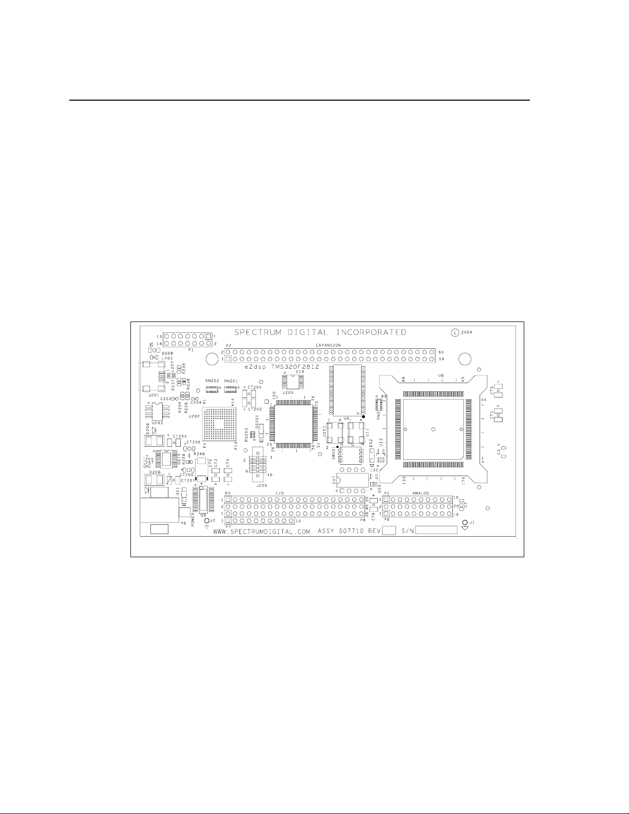
R2812 is a 5.25 x 3.0 inch, multi-layered printed circuit board, powered
by an external 5-Volt only power supply. Figure 2-1 shows the layout of the top side
of the R2812 eZdsp.
Figure 2-1, eZdspTM R2812 PCB Outline
2-2 eZdsp
TM
R2812 Technical Reference
Page 15

Spectrum Digital, Inc
2.1.1 Power Connector
TM
The eZdsp
unit. The unit requires 500mA. The power is supplied via connector P6. If expansion
boards are connected to the eZdsp, a higher amperage power supply may be
necessary. Section 2.3.6 provides more information on connector P6.
R2812 is powered by a 5-Volt only power supply, included with the
2.2 eZdsp
TM
R2812 Memory
The eZdsp includes the following on-chip memory:
• 2 blocks of 4K x 16 single access RAM (SARAM)
• 1 block of 8K x 16 SARAM
• 4 blocks of 1K x 16 SARAM
In addition 64K x 16 off-chip SRAM is provided. The processor on the eZdsp can be
configured for boot-loader mode or non-boot-loader mode.
For bootloading user code a 256K bit serial EEPROM is provided
The eZdsp can load ram for debug, or EEPROM can be loaded and run. For larger
software projects it is suggested to do a initial debug with on eZdsp R2812 module
which supports a total RAM environment. With careful attention to the I/O mapping in
the software the application code can easily be ported to the R2812.
The table below shows the external chip select signal and its use.
Table 1: External Chip Select and Usage
Chip Select
Signal
Use
XZCS0AND1n Expansion header
XZCS2n Expansion Header
XZCS6AND7n External SRAM
2 -3
Page 16

Spectrum Digital, Inc
2.2.1 Memory Map
The figure below shows the memory map configuration on the eZdsp
TM
R2812.
Figure 2-2, eZdspTM R2812 Memory Space
2-4 eZdsp
TM
R2812 Technical Reference
Page 17

Spectrum Digital, Inc
2.2.2 External Memory Timing
This section describes the timing for the external memory bus when the R2812 is
operating at 150 Mhz. In addition a segment of ‘C’ code is provided to configure the
EMIF.
Table 2: External Memory Timing
Memory
Function
Write Cycle Time 40.4ns
Write Low Time 14.0ns
Write High Time 26.4ns
Read Cycle Time 60.8ns
Read Low Time 26.8ns
Read High Time 34.0ns
The following ‘C’ code segment will initialize the EMIF for 150 Mhz operation.
#define XINTCNF2 ( 0x13 )
#define XWRTRAIL(x) ((x & 3))
#define XWRACTIVE(x) ((x & 7)<<2)
#define XWRLEAD(x) ((x & 3)<<5)
#define XRDTRAIL(x) ((x & 3)<<7)
#define XRDACTIVE(x) ((x & 7)<<9)
#define XRDLEAD(x) ((x & 3)<<12)
#define USEREADY (1<<14)
#define ASYNCREADY (1<<15)
#define XTIMING6 (XWRTRAIL(2) | \
XWRACTIVE(1) | \
XWRLEAD(2) | \
XRDTRAIL(2) | \
XRDACTIVE(3) | \
XRDLEAD(2) )
Time in ns.
XINTF_Init()
{
*(unsigned long *)0xB2C = (unsigned long)XTIMING6;
*(unsigned long *)0xB34 = (unsigned long)XINTCNF2;
}
2 -5
Page 18

Spectrum Digital, Inc
2.3 eZdspTM R2812 Connectors
The eZdsp
TM
R2812 has five connectors. Pin 1 of each connector is identified by a
square solder pad. The function of each connector is shown in the table below:
Table 3: eZdsp
TM
R2812 Connectors
Connector Function
P1 JTAG Interface
P2 Expansion
J201
USB Controller
Interface
P4/P8/P7 I/O Interface
P5/P9 Analog Interface
P6 Power Connector
The diagram below shows the position of each connector
P1
P2
J201
P6
P4/P8/P7
Figure 2-3, eZdspTM R2812 Connector and Switch Positions
2-6 eZdsp
SW501
TM
R2812 Technical Reference
P5/P9
Page 19

Spectrum Digital, Inc
2.3.1 P1, JTAG Interface
TM
The eZdsp
standard interface used by JTAG emulators to interface to Texas Instruments DSPs.
The positions of the 14 pins on the P1 connector are shown in the diagram below as
viewed from the top of the eZdsp.
R2812 is supplied with a 14-pin header interface, P1. This is the
1
P1
Fig 2-4, P1 Pin Locations
The definition of P1, which has the JTAG signals is shown below.
Table 4: P1, JTAG Interface Connector
Pin # Signal Pin # Signal
1
3
5
7
9
11 TCK 12 GND
13
TMS 2TRST-
TDI 4GND
PD (+5V) 6 no pin
TDO 8GND
TCK-RET 10 GND
EMU0 14 EMU1
2
2 -7
Page 20

Spectrum Digital, Inc
The TMS320R2812 supports +3.3V Input/Output levels
which are NOT +5V tolerant. Connecting the eZdsp to
a system with +5V Input/Output levels will damage the
TMS320R2812. If the eZdsp is connected to another
target then the eZdsp must be powered up first and
powered down last to prevent lactchup conditions.
2.3.2 P2, Expansion Interface
The positions of the 60 pins on the P2 connector are shown in the diagram below as
viewed from the top of the eZdsp.
P2
2
6
1
345
12
16
14
10
8
7
13
11
15
9
171819
WARNING !
303132
29
34
33
20
262728
22
24
21
25
23
40
36
38
39
35
37
46
42
41
48
44
43
45
47
54
52
50
49
56
58
60
51
53
55
59
57
Figure 2-5, Connector P2 Pin Locations
2-8 eZdsp
TM
R2812 Technical Reference
Page 21

Spectrum Digital, Inc
The definition of P2, which has the I/O signal interface is shown below.
Table 5: P2, Expansion Interface Connector
Pin # Signal Pin # Signal
1 +3.3V/+5V/NC * 2 +3.3/+5V/NC *
3XD04XD1
5XD26XD3
7XD48XD5
9XD610XD7
11 XD8 12 XD9
13 XD10 14 XD11
15 XD12 16 XD13
17 XD14 18 XD15
19 XA0 20 XA1
21 XA2 22 XA3
23 XA4 24 XA5
25 XA6 26 XA7
27 XA8 28 XA9
29 XA10 30 XA11
31 XA12 32 XA13
33 XA14 34 XA15
35 GND 36 GND
37 XZCS0AND1n 38 XZCS2n
39 XREADY 40 10K Pull-up
41 XRnW 42 10K Pull-up
43 XWE 44 XRDn
45 +3.3V 46 XNMI/INT13
47 XRSn/RSn 48 No connect
49 GND 50 GND
51 GND 52 GND
53 XA16 54 XA17
55 XA18 56 XHOLDn
57 XHOLDAn 58 No connect
59 No connect 60 No connect
* Default is No Connect (NC). User can jumper to +3.3V or +5V on backside of eZdsp
with JP5.
2 -9
Page 22

Spectrum Digital, Inc
2.3.3 P3, USB Port/JTAG Interface
The eZdsp
direct access to the integrated JTAG interface. Drivers for C2000 Code Composer tools
are shipped with the eZdsp modules
2.3.4 P4/P8/P7, I/O Interface
The connectors P4, P8, and P7 present the I/O signals from the DSP. The layout of
these connectors are shown below.
TM
R2812 uses a custom USB port JTAG interface device. The device has
2
1
2
1
1
4
3
4
3
2
10
6
5
7
3
4
56
12
11
9
5
6
7
141516
13
788
10
8
11 12
9
22
18
20
17
19
21
10
9
P7
13
242526
23
15 16
14 17
282930
32
31
333435
27
18
36
19
383940
37
20
P4
P8
Figure 2-6, P4/P8/P7 Connectors
2-10 eZdsp
TM
R2812 Technical Reference
Page 23

Spectrum Digital, Inc
The pin definition of P4/P8 connectors are shown in the table below.
Table 6: P4/P8, I/O Connectors
P4
Pin #
1
2
3
4
5
6
7
8
9
10
11
12
13
14
15
16
17
18
P4 Signal
+3.3V/+5V/NC * 1 +3.3V/+5V/NC * 2 +3.3V/+5V/NC *
XINT2/ADCSOC 3 SCITXDA 4 SCIRXDA
MCLKXA 5 XINT1n/XBIOn 6 CAP1/QEP1
MCLKRA 7 CAP2/QEP2 8 CAP3/QEPI1
MFSXA 9 PWM1 10 PWM2
MFSRA 11 PWM3 12 PWM4
MDXA 13 PWM5 14 PWM6
MDRA 15 T1PWM/T1CMP 16 T2PWM/T2CMP
No connect 17 TDIRA 18 TCLKINA
GND 19 GND 20 GND
CAP5/QEP4 21 No connect 22 XINT1N/XBIOn
CAP6/QEPI2 23 SPISIMOA 24 SPISOMIA
T3PWM/T3CMP 25 SPICLKA 26 SPISTEA
T4PWM/T4CMP 27 CANTXA 28 CANRXA
TDIRB 29 XCLKOUT 30 PWM7
TCLKINB 31 PWM8 32 PWM9
XF/XPLLDISn 33 PWM10 34 PWM11
SCITXDB 35 PWM12 36 CAP4/QEP3
P8
Pin #
P8 Signal
P8
Pin #
P8 Signal
19
20
2-1 1
SCIRXDB 37 T1CTRIP/PDPINTAn 38 T3CTRIP/PDPINTBn
GND 39 GND 40 GND
* Default is No Connect (NC). User can jumper to +3.3V or +5V on backside of eZdsp
with JP4.
Page 24

Spectrum Digital, Inc
The pin definition of P7 connector is shown in the table below.
Table 7: P7, I/O Connector
2.3.5 P5/P9, Analog Interface
The position of the 30 pins on the P5/P9 connectors are shown in the diagram below
as viewed from the top of the eZdsp.
P7
Pin #
1C1TRIPn
2C2TRIPn
3C3TRIPn
4 T2CTRIPn/EVASOCn
5C4TRIPn
6C5TRIPn
7C6TRIPn
8 T4CTRIPn/EVBSOCn
9 No connect
10 GND
P7 Signal
P5
1
2
P9
Figure 2-7, Connector P5/P9 Pin Locations
2-12 eZdsp
3
2
6
4
531
ANALOG
5
4
10
8
9
7
12
7
6
14
1311
8
16
15
9
10
18
20
19
17
TM
R2812 Technical Reference
Page 25

Spectrum Digital, Inc
The definition of P5/P9 signals are shown in the table below.
Table 8: P5/P9, Analog Interface Connector
P5
Pin #
1
2
3
4
5
6
7
8
9
10
Signal
ADCINB0 1 GND 2 ADCINA0
ADCINB1 3 GND 4 ADCINA1
ADCINB2 5 GND 6 ADCINA2
ADCINB3 7 GND 8
ADCINB4 9 GND 10
ADCINB5 11 GND 12 ADCINA5
ADCINB6 13 GND 14 ADCINA6
ADCINB7 15 GND 16 ADCINA7
ADCREFM 17 GND 18 VREFLO *
ADCREFP 19 GND 20 No connect
P9
Pin #
Signal
P9
Pin #
Signal
ADCINA3
ADCINA4
* Connect VREFLO to AGND or VREFLO of target system for proper ADC operation.
2-1 3
Page 26

Spectrum Digital, Inc
2.3.6 P6, Power Connector
Power (5 volts) is brought onto the eZdsp
TM
R2812 via the P6 connector. The
connector has an outside diameter of 5.5 mm. and an inside diameter of 2.5 mm. The
position of the P6 connector is shown below.
PC Card Edge
P6
Figure 2-8, Connector P6 Location
The diagram of P6, which has the input power is shown below.
+5V
P6
Ground
PC Board
Front View
Figure 2-9, eZdsp
TM
R2812 Power Connector
2-14 eZdsp
TM
R2812 Technical Reference
Page 27

Spectrum Digital, Inc
2.3.7 Connector Part Numbers
The table below shows the part numbers for connectors which can be used on the
TM
eZdsp
R2812. Part numbers from other manufacturers may also be used.
2.4 eZdsp
Table 9: eZdsp
TM
R2812 Suggested Connector Part Numbers
Connector Male Part Numbers Female Part Numbers
P1 SAMTEC TSW-1-10-07-G-T SAMTEC SSW-1-10-01-G-T
P2 SAMTEC TSW-1-20-07-G-T SAMTEC SSW-1-20-01-G-T
*SSW or SSQ Series can be used
TM
R2812 Jumpers
The eZdsp
TM
R2812 has 2 jumpers, JP4 and JP5, which will allow power to be
supplied to the expansion headers. The table below lists the jumpers and their
function. The following sections describe the use of each jumper.
Table 10: eZdsp
TM
R2812 Jumpers
Position As
Jumper # Size Function
Shipped From
Factory
JP4 1 x 3 +3.3/5 Volts to P8,P4 Not connected
JP5 1 x 3 +3.3/5 Volts to P2 Not Connected
2-1 5
Page 28

Spectrum Digital, Inc
2.4.1 JP4, JP5 Voltage Jumpers
Jumpers JP4 and JP5 are unpopulated jumpers on the bottom side of the board that
provide either +3.3 volts or +5 volts to pins on the expansion connectors. These
jumpers are shipped uninstalled to prevent accidental damage by connecting wires or
circuitry to the expansion connector. The user may connect these jumpers by installing
a jumper wire or zero ohm resistor. The position of these jumpers are shown in the
figure below.
JP5
Figure 2-10, eZdspTM R2812 Voltage Jumper Positions (Bottom Side)
2-16 eZdsp
JP4
TM
R2812 Technical Reference
Page 29

Spectrum Digital, Inc
2.4.1.1 JP4, +3.3/5 Volts for P8, P4
Jumper JP4 allows the user to provide either +3.3 or +5 volts to pins 1 and 2 of
expansion connector P8, and pin 1 of P4. The settings for this jumper are shown in the
table below
Table 11: JP4, +3.3/5 Volts for P8, P4
Position Function Jumper Position
Middle - Bottom
Middle - Top
No connect *
* As shipped from factory
Connect +5 Volts
to P8, pins 1,2,
and P4 pin1
Connect +3.3
Volts to P8, pins
1,2, and P4 pin1
3.3V
JP4
5V
3.3V
JP4
5V
3.3V
JP4
5V
+3.3V
JP4
+5V
P4, pin 1
Figure 2-11, JP4 Layout
2-1 7
Page 30

Spectrum Digital, Inc
2.4.1.2 JP5, +3.3/5 Volts for P2
Jumper JP5 allows the user to provide either +3.3 or +5 volts to pins 1 and 2 of
expansion connector P2. The settings for this jumper are shown in the table below.
Position Function Jumper Position
Middle - Right Connect +5 Volts to P2,
Middle - Left Connect +3.3 Volts to P2,
No connect *
Table 12: JP5, +3.3/5 Volts for P2
Pins 1,2
pins 1,2
JP5
JP5
JP5
+3.3V
+3.3V
+3.3V
+5V
+5V
+5V
* As shipped from factory
JP5
+3.3V
Figure 2-12, JP5 Layout
P2, pin 1
+5V
2-18 eZdsp
TM
R2812 Technical Reference
Page 31

Spectrum Digital, Inc
2.5 Switch SW501
The eZdsp R2812 has a 4 position switch that allows the user to configure the board for
their application. The function of each position is shown in the table below.
Table 13: SW501 Switch Positions
Position Function
1 PLL Enable/Disable
2 MP/MC Select
3, 4 Boot Mode Select
1
2
3
SW501
4
Open/High | Closed/Low
Default from factory
Figure 2-13, SW501 Layout
2.5.1 Switch SW501, Position 1, PLL Enable/Disable
Position 1 on switch SW501 is used to enable/disable the use of the Phase Lock Loop
(PLL) logic on the DSP. The selection of the open position enables the use of the PLL.
If the closed position is used the PLL is disabled. This signal is latched at reset and
may be used as XF after reset. The positions are shown in the table below.
Table 14: SW501, Position 1
Position Function
Open-1 * PLL Enabled
Closed-0 PLL disabled
XF_XPLLDISn
XMP_MCn
SPICLKA
MDXA
* as shipped from the factory
2-1 9
Page 32

Spectrum Digital, Inc
2.5.2 Switch SW501, Position 2, XMP/MCn Mode Select
Position 2 on switch SW501 is used to select the XMP/MCn option. The open selection
allows the DSP to operate in the Microprocessor mode. The closed selection allow
the DSP to operate in the Microcontroller mode. The positions are shown in the table
below.
Table 15: SW501, Position 2
Position Function
Open-1 Microprocessor mode
Closed-0 * Microcontroller mode
* as shipped from factory
2.5.3 Switch SW501, Position 3, 4, Boot Mode Select
Positions 3 and 4 on switch SW501 along with position 2 are used to determine what
mode the DSP will use for bootloading on power up. The options are shown in the
table below.
Table 16: SW501, Position 3, 4
Position 2
XMP_MCn
Closed-0 Open-1 Do not care SPI *
Closed-0 Closed-0 Open-1 SCI
Closed-0 Closed-0 Closed-0 H0
Open-1 Do not care Do not care Microprocessor
Position 3
SPICLKA
Position 4
MDXA
Boot
Mode
Mode
* factory default
2-20 eZdsp
TM
R2812 Technical Reference
Page 33

Spectrum Digital, Inc
2.6 LEDs
TM
The eZdsp
+5 volts and is normally ‘on’ when power is applied to the board. DS2 is under software
control and is tied to the XF pin on the DSP through a buffer. These are shown in the
table below.
2.7 Test Points
R2812 has two light-emitting diodes. DS1 indicates the presence of
Table 17: LEDs
LED # Color Controlling Signal
DS1 Green +5 Volts
DS2 Green XF bit (XF high = on)
The eZdsp
table below.
TM
R2812 has two test points. The signals they are tied to are shown in the
Table 18: Test Points
Test Point Signal
J1 Analog Ground
J2 Ground
2-2 1
Page 34

Spectrum Digital, Inc
2-22 eZdsp
TM
R2812 Technical Reference
Page 35

Appendix A
TM
eZdsp
Schematics
The schematics for the eZdspTM R2812 can be found on the CD-ROM that
accompanies this board. The schematics were drawn on ORCAD.
WARNING !
The TMS320R2812 supports +3.3V Input/Output levels
which are NOT +5V tolerant. Connecting the eZdsp to
a system with +5V Input/Output levels will damage the
TMS320R2812. If the eZdsp is connected to another
target then the eZdsp must be powered up first and
powered down last to prevent lactchup conditions.
R2812
A -1
Page 36

Spectrum Digital, Inc
1
of
16Friday, May 28, 2004
1
REVI SI ONS
DESCRI PT I ONREV DATE APPROVED
2
The TMS320R2812EzDSP design is based on
preliminary information(SPRS174G) for the
TMS320F2812 device. This schematic is subject
to change without notification. Spectrum Digital
Inc. assumesno liabilityfor applications
assistance,customer product design or
infringement of patents described herein.
507712 A
TMS320R2812 EzDSP USB
B
Title
Size Document Number Re v
SPECTRUM DIGITAL
Date: Sheet
2
APROTOTYPES 29-April-2004
3
DATE
DATE
DATE
DATE
3
DATE
DATE
DATE
4
ENGR-MGR
ENGR
CHK
DWN
5
REVI SI ON STATUS OF SHEETS
REV
D D
C C
B B
SH
A A
4
QA
RLS E
MF G
NEXT ASSY
A
62
5
A
5
4
AUSEDON
A
3
A
A
1APPLICATION
REV
SH
SH
REV
A-2 eZdspTM R2812 Technical Reference
Page 37

Spectrum Digital, Inc
XREADY 4
XRnW 4
XZCS2n 4
XMP_MCn 4
XHOLDn 4
XZCS0AND1n 4
RN33
16
XD[0..15] 3,4
XA[0..18] 3,4
1
XD0
XD1
XD2
XD3
XD4
XD5
XD6
XD7
XD8
XD9
XD10
XD11
68
XD021XD124XD227XD330XD433XD536XD639XD754XD865XD9
XA18
158
XA18
XA17
156
XA17
XA16
152
XA16
XA15
148
XA15
XA14
144
XA14
XA13
141
XA13
XA12
138
XA12
XA11
132
XA11
XA10
130
XA10
XA9
125
XA9
XA8
121
XA8
XA7
118
XA7
XA6
111
XA6
2
1.8V4,6
3
XA5
108
XA5
XA4
103
XA4
XA3
85
XA3
XA2
80
XA2
XA1
43
XA1
XA0
18
XA0
VDD10
154
VDD9
143
VDD8
128
VDD7
112
VDD6
100
VDD5
75
VDD4
56
VDD3
37
VDD2
23
VDDIO5
145
VDDIO4
114
VDDIO3
81
VDDIO2
64
VDDIO1
31
VDD3VFL
69
XD1073XD1174XD1296XD1397XD14
VDD CORE - 1 . 8 V
VDD I / 0 - 3 . 3 V
FLASH - 3. 3V
15
B
B
A
A
1
2
RN2A
RN2B
XD12
XD13
XD14
XD15
44
139
147
88
XD15
XZCS2n
XZCS0AN D1n
XHOLDAn 4
XWEn 3,4
XZCS6AND7n 3
RN33
RN33
14
B
A
3
RN2D
RN2C
133
XZCS6AN D7n
XRSn 5
X1_CLKIN 4
XRDn 3,4
RN33
RN33
RN33
13
12
11
B
B
B
A
A
A
4
5
6
RN2E
RN2F
42
161
84
51
XRDn
XWEn
XRnW
XCLKOUT 4
XTESTSEL 3, 4,5, 6
C28_TRSTn 5
C28_EMU1 5
C28_EMU0 5
C28_TCK 5
C28_TMS 5
SPISIMOA 3,4
SPISOMIA 3,4
SPICLKA 3,4
SPISTEA 3,4
C28_TDO 5
C28_TDI 5
SCITXDA 4
SCIRXDA 4
CANTXA 4
MCLKXA 4
MCLKRA 4
MFSXA 4
MFSRA 4
MDXA 4
MDRA 4
CANRXA 4
XF_XPLLDISn 4
SCITXDB 4
SCIRXDB 4
DSP
66
119
82
159
17
160
76
77
X2
XRSn
XHOLDn
XREADY
XMP/MCn
XHOLDAn
X1/XCLKI N
126
134
136
131
135
TCK
TMS
TEST167TEST2
TRSTn
TESTSEL
XCLKOUT
35
127
137
146
TDI
TDO
EMU0
EMU1
26
28
34
29
41
25
GPIOF10-MFSXA
GPIOF11-MFSRA
GPIOF8-MCLKXA
GPIOF9-MCLKRA
GPIOF3-SPISTEA
GPIOF2-SPICLKA
GPIOF0-SPISIMOA40GPIOF1-SPISOMIA
91
157
87
20
22
GPIOF12-MDXA
GPIOF13-MDRA
89
155
GPIOF4-SCITXDA
140
90
GPIOF6-CANTXA
GPIOF7-CANRXA
GPIOF5-SCIRXDA
GPIOG4-SCITXDB
GPIOG5-SCIRXDB
GPIOF14-XF-XPLLDISn
VSS16
153
VSS15
142
VSS14
129
VSS13
120
VSS12
113
VSS11
105
VSS10
99
VSS9
86
VSS8
78
VSS7
70
VSS6
58
VSS5
52
VSS4
38
VSS3
32
VSS2
19
VSSAIO
176
VDDAIO
1
VSS1
ADC
163
1. 8V
VDD1
162
VSSA2
165
VSSA1
15
VDDA2
166
VDDA1
14
of
26Friday , June 11, 2004
1
507712 A
TMS320R2812 EzDSP USB
B
Title
Size Document Number Rev
Date: Sheet
2
3
3.3V
VDD3VFL6
ADCINA0
ADCINA1
ADCINA2
ADCINA3
ADCINA4
ADCINA5
ADCINA6
ADCINA7
173
172
171
170
169
168
ADCINA14
ADCINA24
ADCINA34
ADCINA44
ADCINA54
ADCINB02ADCINB13ADCINB24ADCINB35ADCINB46ADCINB57ADCINB68ADCINB79ADCREFP11ADCREFM10ADCRESEXT16AVSSREFBG12AVDDREFBG13ADCLO
167
ADCINA64
ADCINA74
ADCINB04
ADCINB14
ADCINB24
ADCINB34
ADCINB44
ADCINB54
ADCINB64
ADCINB74
U8
174
4
ADCINA04
ADCBGREFIN
GPIOA0-PWM192GPIOA1-PWM293GPIOA2-PWM394GPIOA3-PWM495GPIOA4-PWM598GPIOA5-PWM6
GPIOA6-T1PWM_T1CMP
GPIOA7-T2PWM_T2CMP
GPIOA8-CAP1_QEP1
GPIOA9-CAP2_QEP2
GPIOA10-CAP3_QEPI1
GPIOA11-TDIRA
GPIOA12-TCLKINA
GPIOA13-C1TRIPn
GPIOA14-C2TRIPn
GPIOA15-C3TRIPn
GPIOB0-PWM745GPIOB1-PWM846GPIOB2-PWM947GPIOB3-PWM1048GPIOB4-PWM1149GPIOB5-PWM1250GPIOB6-T3PWM_T3CMP53GPIOB7-T4PWM_T4CMP55GPIOB8-CAP4_QEP357GPIOB9-CAP5_QEP459GPIOB10-CAP6_QEPI260GPIOB11-TDIRB71GPIOB12-TCLKINB72GPIOB13-C4TRIPn61GPIOB14-C5TRIPn62GPIOB15-C6TRIPn63GPIOD0-T1CTRIP_PDPINTAn
175
164
VDDA1
ADCBGREFIN
101
102
104
106
107
109
116
117
122
123
124
PWM14
PWM24
PWM34
PWM44
TDIRA4
PWM54
PWM64
CAP1_QEP14
CAP2_QEP24
T1PWM_T1CMP4
T2PWM_T2CMP4
PWM74
PWM84
PWM94
PWM104
CAP3_QEPI14
TCLKINA4
C1TRIPn4
PWM114
CAP4_QEP34
CAP5_QEP44
CAP6_QEPI24
T3PWM_T3CMP4
T4PWM_T4CMP4
C2TRIPn4
PWM124
C3TRIPn4
GPIOD1-T2CTRIPn_EVASOCn
GPIOD5-T3CTRIP_PDPINTBn79GPIOD6-T4CTRIPn_EVBSOCn83GPIOE0-XINT1_XBIOn
110
115
TDIRB4
TCLKINB4
C4TRIPn4
C5TRIPn4
C6TRIPn4
T1CTRIP_PDPINTAn4
T3CTRIP_PDPINTBn4
T2CTRIPn_EVASOCn4
TMS320R2812PGF
GPIOE1-XINT2_ADCSOC
GPIOE2-XNMI_XINT13
149
151
150
XINT1n_XBIOn4
XINT2n_ADCSOC4
XNMIn_XINT34
T4TRIPn_EVBSOCn4
VDDA1
C37
R26
24.9K
1 2
1 2
1 2
C35
C36
10UF CERAMIC LOW ESR
10UF CERAMIC LOW ESR
5
GND3,4,5,6
AGND3,4,5,6
ADCREFP4
ADCREFM4
TAIYOYUDEN EMK325F106ZH-T
D D
1
TP3
NO-POP
VREFLO4
C C
J1
1
SINGLE POINT CONNECTION
B B
VDD11.8V
C56
0.001uF
12
(1.8V)
C58
NO-POP
12
0.1uF
1uF
C2
L4
BLM21P221SN
0.001uF
12
C38
0.1uF
12
(3.3V)
C57
0.1uF
12
1uF
C3
LOCATENEAR DSP
L3
BLM21P221SN
3.3V
A A
A -3
4
5
Page 38

Spectrum Digital, Inc
1
2
SPISIMOA 2,4
SPICLKA 2,4
SPISIMOA
SPICLKA
3.3V
3
U17
6
7
8
VCC
SCLK
HOLDn
CSn1SO2WPn3GND
5
SIN
4
of
36Frida y, May 28, 2004
1
507712 A
TMS320R2812 EzDSP USB
B
Title
Size Do cumen t Number Re v
Dat e: Sheet
C10
0.1uF
12
C22
XA[0..18] 2,4
XD[0..15] 2,4
AT25HP256/512 (DIP-8 SOCKET)
3.3V
3.3V
ASRAM
12
33
11
0.1uF
U4
XD4
XD1
XD3
XD0
XD7
XD5
XD2
XD6
D07D18D29D310D413D514D615D716D829D9
VDD2
VDD1
A01A12A23A34A45A518A619A720A8
XD10
XD9
XD8
30
A1124A1225A1326A1427A1542A1643A17
21
XD13
XD12
XD11
D1031D1132D1235D1336D1437D15
XD15
XD14
38
28
VSS2
34
VSS1
NC
A922A10
CS6WE17OE41BHE40BLE
23
44
12
IS61LV 6416-12T
39
2
3
SPISOMIA
SPISTEA
XRDn2,4
XWEn2,4
XZCS6AND7n2
XA15
XA10
XA5
XA2
XA1
XA0
XA4
3.3V
SPISTEA2,4
SPISOMIA2,4
4
5
D D
C C
XA3
XA13
XA8
XA9
XA6
XA14
XA7
XA11
XA12
XA16
XA17
4
64Kx16 and 256Kx16
Compatible
5
GND2,4,5,6
B B
A A
A-4 eZdspTM R2812 Technical Reference
Page 39

Spectrum Digital, Inc
3.3V
DS2
1
2
3
TMS320F2812 supports 3.3V
4
+5V
5
1
A
B
JP4
C
3
3.3V
6
Make a solder connection on
JP4and/orJP5 to the
appropriate power supply.
7
+5V
1
A
B
JP5
C
3
3.3V
8
21
input/output levels which are
NOT 5V tolerant. Connecting
theeZdsptoasystemwith5V
input/output levels will damage
the TMS320F2812. If the eZdsp
is connected to another target
SCIRXDA 2
CAP1_QEP1 2
CAP3_QEPI1 2
NO-POP
2
NO-POP
2
10
2
4
6
8
2
4
6
8
P8
1
3
5
7
1
3
5
7
9
SCITXDA2
XINT1n_XBIOn2
CAP2_QEP22
XD1 2,3
XD3 2,3
XD5 2,3
XD7 2,3
10
12
2
4
6
8
2
4
6
8
10
P2
1
3
5
7
9
1
3
5
7
9
11
XD02,3
XD22,3
XD42,3
XD62,3
D D
XF
220
LTST-C150GKT
GREEN
R43
0.1uF
1 2
4
C62
SN74AHC1G14
3
5
U12
3.3V
then the eZdsp must be
poweredup first and powered
down last to prevent latchup
conditions.
PWM2 2
PWM4 2
PWM6 2
SPISOMIA 2,3
SPISTEA 2,3
CANRXA 2
T2PWM_T2CMP 2
TCLKINA 2
XINT1n_XBIOn 2
12
14
16
18
20
22
24
26
10
9
11
PWM12
XD9 2,3
14
12
11
13
XD82,3
28
12
14
16
18
20
22
24
26
28
11
13
15
17
19
21
23
25
27
13
15
17
19
21
23
25
27
TDIRA2
PWM32
PWM52
T1PWM_T1CMP2
SPISIMOA2,3
SPICLKA2,3
CANTXA2
XD11 2,3
XD13 2,3
XD15 2,3
XA1 2,3
XA3 2,3
XA5 2,3
XA7 2,3
XA9 2,3
XA11 2,3
16
18
20
22
24
26
28
30
14
16
18
20
22
24
26
28
30
13
15
17
19
21
23
25
27
29
15
17
19
21
23
25
27
29
XA02,3
XA22,3
XA42,3
XA62,3
XA82,3
XD102,3
XA102,3
XD122,3
XD142,3
XTESTSEL
2
1
XF
XF_XPLLDISn2
C1TRIPn 2
PWM7 2
PWM9 2
PWM11 2
CAP4_QEP3 2
T3CTRIP_PDPINTBn 2
11223344556677889
P7
30
32
34
36
38
40
30
32
34
36
38
40
P4
29
31
33
35
37
39
29
31
33
35
37
39
XCLKOUT2
PWM82
PWM102
PWM122
T1CTRIP_PDPINTAn2
XA13 2,3
XA15 2,3
XZCS2n 2XZCS0AND1n2
STRBn
ISn
32
34
36
38
40
42
32
34
36
38
40
42
31
33
35
37
39
41
31
33
35
37
39
41
XRnW2
XREADY2
XA122,3
XA142,3
112233445566778899101011111212131314141515161617171818191920
XRDn 2,3
XNMIn_XINT3 2
XA17 2,3
XHOLDn 2
44
46
48
50
52
54
56
58
44
46
48
50
52
54
56
58
43
45
47
49
51
53
55
57
43
45
47
49
51
53
55
57
DSP_RSn
XA162,3
XA182
XWEn2,3
3.3V
DSP_RSn5
C C
XTESTSEL 2, 3,5,6
3.3V
MDXA 2
SPICLKA 2,3
XMP_MCn 2
XF_XPLLDISn 2
1 2
1 2
1 2
1 2
R39 20K
R31 20K
R40 20K
R42 20K
BOOT-0
BOOT-2
PLLDISn
MPMC n
876
5
SW501
SW DIP-4/SM
123
C2TRIPn 2
C3TRIPn 2
C4TRIPn 2
C5TRIPn 2
C6TRIPn 2
T4TRIPn_EVBSOCn 2
T2CTRIPn_EVASOCn 2
9
10
10
MDXA2
MDRA2
MFSXA2
MFSRA2
MCLKXA2
MCLKRA2
XINT2n_ADCSOC2
60
60
NO-POP
59
59
XHOLDAn2
TDIRB2
CAP5_QEP42
CAP6_QEPI22
T3PWM_T3CMP2
T4PWM_T4CMP2
TCLKINB2
XF_XPLLDISn2
ADCINA0 2
ADCINA1 2
ADCINA2 2
ADCINA3 2
ADCINA4 2
ADCINA5 2
ADCINA6 2
ADCINA7 2
10
12
14
16
2
4
6
8
2
4
6
8
10
12
14
P9
1
3
5
7
9
11
13
1
3
5
7
9
11
13
15
4
1 2
1 2
1 2
R41 2.2K
R36 2.2K
R37 2.2K
20
SCITXDB2
SCIRXDB2
Connect VREFLO to AGND or
to VREFLO of target system
for proper ADC operation.
VREFLO 2
ADCINB0 2
ADCINB1 2
ADCINB2 2
ADCINB3 2
18
20
11223344556677889
16
18
20
P5
15
17
19
17
19
B B
ADCINB4 2
L1
ADCINB5 2
ADCINB6 2
MODE
BOOT-3 BOOT-2 BOOT-1 BOOT-0
SCITXDA MDXA SPISTEA SPICLKA
BOOT-3
JP7
JUMPER3_SMT
A
1
3.3V
1.8V 2,6
C43
BLM21P221SN
ADCINB7 2
ADCREFP 2
ADCREFM 2
10
9
10
FLASH
SCIH0OTP
SPI
X
0
1
X
X
1
1
XX
000
1
00000
1
SCITXDA 2
DEFAULT IS BC FOR NON-FLASHBOOT
2
C
3
B
1
OFFn
0.1uF
VCC4CLK
U11
1 2
Tie off unused F24xx
compatiblesignals.
PARALLEL
1
0
00
0
BOOT-1
JP11
JUMPER3_SMT
2
A
1
3.3V
2
GND
30MHz
3
C42
12
100
R29
X1_CLKIN2
3.3V
10K
R5
R6
1 2
ISn
A A
507712 A
TMS320R2812 EzDSP USB
B
Title
Size Do cumen t Number Re v
SPISTEA 2 ,3
DEFAULT IS AB FOR S PI/SCI/H0
C
3
B
SMT/4PINDIP
NO-POP
1 2
AGND2,3,5,6
10K
GND 2,3,5,6
1 2
GND
STRBn
A -5
of
1
46Thursday , June 10, 2004
2
Dat e: Sheet
3
4
5
6
7
8
Page 40

Spectrum Digital, Inc
12
+5V
R80
1.5K
3
2 1
1
D2
XDS_4.1V
12
0.1uF
C80
+5V
2
3.3V
10K
10K
R13
LM4040DCIM3-4.1
1 2
R16
1 2
3.3V
JP2
JUMPER3_SMT
A
C
1
3
B
2
of
C28_TRSTn 2
C28_TMS 2
C28_TDI 2
C28_TCK 2
R20
100
C4
22pF
12
10K
10K
1 2
R14
R22
1 2
Locat e nea r DSP TCK
pi n
C28_TDO 2
C28_EMU0 2
C28_EMU1 2
56Friday, Ma y 28, 2004
1
R19 33
507712 A
16
4
7
12
1A
8
2A
3A94A
VCC
1B1
U19
2
GND
4B1
3B1
4B213S
OE
3B2101B232B152B2
SN74CBT3257PW
1
6
14
11
15
3.3V
1
53
U26
2
4
3.3V
10K
10K
1 2
1 2
R11
R12
TMS320R2812 EzDSP USB
B
Title
Size Document Number Re v
Date: Sheet
2
SN74LVC1G32
XTPD
1
3
5
7
9
11
13
1
3
5
7
9
P1
11
13
2
4
6
8
10
12
3
4
5
14
2
5V
+5V
HEADER7X2
4
6
8
10
12
14
GND 2,3,4,6
3.3V
GND
3.3V
XTRSTn
XTMS
XTDI
XTCK
USBSEL
USBS EL - HI GH, SEL ECT USB EMUL ATI ON
USBS EL - L OW, S ELECT XDS EMULATI ON
10K
T_TRSTn
T_TMS
T_TDI
T_TCK
R17
1 2
3.3V
XRSn 2
XRSn i s logi ca l AND of PONRSnIN and
emulator controlled reset. Power on default
is PONRnIN controls XRSn.
for best EMI/ESD noise immunity.
Locate R7,R54, C70 at the DSP XRSn pin
12
3.3V
I F U13 I S I NSTALLED THEN
C70
22nF
12
R54
100
R7
1.5K
R18 33
3
T_TCK_RET
T_TDO
T_EMU0
T_EMU1
PONRSnIN 6
4
T_TDI
T_TCK
T_TDO
T_TMS
T_EMU0
T_EMU1
T_TRSTn
3.3V
DSP_RS_OUT_ODn
USB1
DSP_RSn 4
REMOVE R4 9 A ND R4 8.
To/ f r om e x pans i on header
3.3V
RESET_INn
T_TCK_RET
GND
5V
Embedded_USB
5
+5V
D D
C C
B B
A A
A-6 eZdspTM R2812 Technical Reference
Page 41

Spectrum Digital, Inc
1.8V 2,4
3.3V
1
2
C64
0.1uF
CT3
22uF
+
12
16.9K1.848V
15.0K1.773V
13.7K1.722V
18.2K1.899V
1 2
R45 30.1K, 1%
R33
18.2K, 1 %
12
3
28
1RESET
1INA51INB61EN41GND32INA112INB122EN102GND9NC11NC22NC37NC48NC513NC6
U9
22
25
24
1OUTA231OUTB
2RESET
1FB/SENSE
1.8VONn
4
C66
0.1uF
47uF
220
C65
12
DS1
LTST-C150GKT
GREEN
21
12
CT2
+
12
R44
12
5
+5V
CENTER
SHUNT
SLEEVE
18
2OUTA172OUTB
0.1uF
C63
CT4
22uF
+
12
19
2SENSE
R46
10K
12
VDD3VFL 2
12
C7
0.1uF
1uF
C1
PONRSnIN
of
66Thursday, June 10, 2004
1
J2
1
NO-POP
507712 A
12
0
R52
10K
R2
3.3V
1 2
GND2,3,4,5
1065mW
333mA
TMS320R2812 EzDSP USB
B
Title
Size Document Number Re v
Date: Sheet
521mW
1586mW Total
2
307mA
TPS767D301 RATI NGS
= (125 - 35)/27.9
0.1uF
1.8V
3.3V
VOLTAGE SUPPLY MAX CURRENT TPS767D301PD
MAX Iout PER CHANNEL IS 1A
TPS767D301PD = (Vin-Vout)*Iout
1.8V 2,4
27
NC1215NC1116NC10
3.3V
20
NC921NC826NC7
12
THERMAL_PAD
14
R53
29
TPS767D301
BSS138
Q3
DS
1.5K 1%
G
12
TIE TPS767D301 POWER PAD TO GN D
PLANE (TI- SLMA002)
2.0K 1%
R34
C59
12
C61
12
C40
12
C41
12
C21
12
C8
12
C5
12
C18
12
C19
12
CT5
+
12
CT6
+
12
0.1uF
0.1uF
0.1uF
1.8V SUPPLY
0.1uF
0.1uF
3.3V
C60
0.1uF
0.1uF
0.1uF
0.1uF
0.1uF
22uF
12
12
12
12
12
CT1
+
12
C39
0.1uF
C9
0.1uF
C6
0.1uF
C20
0.1uF
22uF
22uF
Q3
2.2V
3.3V SUPPLY, VDDIO
VDD3VFL, VDDA1,VDDA2
PONRSnIN, GO E S HI GH > 200ms AFTER ALL POW ER
IS STABLE.
3.3V THEN 1.8V
POWERONSEQUENCENOTES
SET Q3 TO TURN ON W HEN 3.3V SUPPLY IS
GREATER THEN 2.2 VOLTS. REGULATOR
TURN ON DELAY AND RAMP RATE W ILL
= 3255mW
PD(max)= (Tj(max) - Ta)/Rja
3
140ms-280ms
4
PONRSnIN
5
ENSURE TH AT 3.3V SUPPLY IS AT 2.5 VOLTS
OR HIGHER BEFORE THE 1.8V SUPPLY
REACHES 0.3 VOLTS.
U16 WILL TURN OFF THE 1.8V SUPPLYWHEN
INPUT POWER FALLS BELOW 2.94V. THIS SPEEDS
UPTHE1.8VSUPPLYTURNOFF.
+5V Max
P6
RASM712
D D
Power sequence is optional for the
TMS320R2812 as it does not include
on-chip FLASH. The regulator 1EN (pin
4) on the could have been
connected to ground for TMS320R2812
only operation.
C C
B B
A A
A -7
Page 42

Spectrum Digital, Inc
A-8 eZdspTM R2812 Technical Reference
Page 43

Appendix B
TM
eZdsp
R2812
MechanicaI Information
This appendix contains the mechanical information about the socketed and
TM
unsocketed versions of the eZdsp
R2812
B-1
Page 44

Spectrum Digital, Inc
This drawing is not to scale
B-2 eZdspTM R2812 Technical Reference
Page 45

Page 46

Printed in U.S.A., September 2004
507715-0001 Rev. B
 Loading...