

Page 1

MC.31xx
fast 12 bit transient recorder,
A/D converter board
for CompactPCI bus
Hardware Manual
Software Driver Manual
English version April 27, 2006
SPECTRUM SYSTEMENTWICKLUNG MICROELECTRONIC GMBH · AHRENSFELDER WEG 13-17 · 22927 GROSSHANSDORF · GERMANY
PHONE: +49 (0)4102-6956-0 · FAX: +49 (0)4102-6956-66 · E-MAIL: info@spec.de · INTERNET: http://www.spectrum-instrumentation.com
Page 2

(c) SPECTRUM SYSTEMENTWICKLUNG MICROELECTRONIC GMBH
AHRENSFELDER WEG 13-17, 22927 GROSSHANSDORF, GERMANY
SBench is a registered trademark of Spectrum Systementwicklung Microelectronic GmbH.
Microsoft, Visual C++, Visual Basic, Windows, Windows 98, Windows NT, Window 2000 and Windows XP are trademarks/registered
trademarks of Microsoft Corporation.
LabVIEW, DASYLab, Diadem and LabWindows/CVI are trademarks/registered trademarks of National Instruments Corporation.
MATLAB is a trademark/registered trademark of The Mathworks, Inc.
Agilent VEE, VEE Pro and VEE OneLab are trademarks/registered trademarks of Agilent Technologies, Inc.
FlexPro is a registered trademark of Weisang GmbH & Co. KG.
Page 3

Introduction....................................................................................................................... 6
Preface ............................................................................................................................................................................... 6
General Information ............................................................................................................................................................. 6
Different models of the MC.31xx series................................................................................................................................... 7
Additional options................................................................................................................................................................ 9
Digital inputs.................................................................................................................................................................. 9
Extra I/O (Option -XMF).................................................................................................................................................. 9
Starhub ....................................................................................................................................................................... 10
Timestamp ................................................................................................................................................................... 10
The Spectrum type plate ...................................................................................................................................................... 11
Hardware information......................................................................................................................................................... 12
Block diagram.............................................................................................................................................................. 12
Dynamic Parameters ..................................................................................................................................................... 13
Order information......................................................................................................................................................... 13
Hardware Installation ..................................................................................................... 14
System Requirements .......................................................................................................................................................... 14
Warnings.......................................................................................................................................................................... 14
ESD Precautions ........................................................................................................................................................... 14
Cooling Precautions...................................................................................................................................................... 14
Sources of noise ........................................................................................................................................................... 14
Installing the board in the system.......................................................................................................................................... 14
Installing a single board without any options.................................................................................................................... 14
Installing a board with digital inputs/outputs.................................................................................................................... 15
Installing a board with extra I/O (Option -XMF) ............................................................................................................... 15
Installing multiple boards synchronized by starhub............................................................................................................ 16
Installing multiple synchronized boards ........................................................................................................................... 17
Software Driver Installation............................................................................................. 18
Interrupt Sharing ................................................................................................................................................................ 18
Windows 98 ..................................................................................................................................................................... 19
Installation ................................................................................................................................................................... 19
Version control ............................................................................................................................................................. 19
Driver - Update............................................................................................................................................................. 20
Windows 2000 ................................................................................................................................................................. 21
Installation ................................................................................................................................................................... 21
Version control ............................................................................................................................................................. 21
Driver - Update............................................................................................................................................................. 22
Windows XP...................................................................................................................................................................... 23
Installation ................................................................................................................................................................... 23
Version control ............................................................................................................................................................. 23
Driver - Update............................................................................................................................................................. 24
Windows NT..................................................................................................................................................................... 25
Installation ................................................................................................................................................................... 25
Adding boards to the Windows NT driver ....................................................................................................................... 25
Driver - Update............................................................................................................................................................. 25
Linux................................................................................................................................................................................. 26
Overview .................................................................................................................................................................... 26
Installation ................................................................................................................................................................... 26
Software ......................................................................................................................... 28
Software Overview............................................................................................................................................................. 28
First Test with SBench.......................................................................................................................................................... 28
C/C++ Driver Interface....................................................................................................................................................... 29
Header files ................................................................................................................................................................. 29
Microsoft Visual C++ .................................................................................................................................................... 29
Borland C++ Builder ..................................................................................................................................................... 29
Linux Gnu C................................................................................................................................................................. 29
Other Windows C/C++ compilers ................................................................................................................................. 30
National Instruments LabWindows/CVI........................................................................................................................... 30
Driver functions ............................................................................................................................................................ 30
Delphi (Pascal) Programming Interface .................................................................................................................................. 32
Type definition ............................................................................................................................................................. 32
Include Driver............................................................................................................................................................... 32
Examples..................................................................................................................................................................... 32
Driver functions ............................................................................................................................................................ 32
Visual Basic Programming Interface ...................................................................................................................................... 34
Include Driver............................................................................................................................................................... 34
Visual Basic Examples................................................................................................................................................... 34
VBA for Excel Examples ................................................................................................................................................ 34
Driver functions ............................................................................................................................................................ 34
3
Page 4

Programming the Board .................................................................................................. 36
Overview .......................................................................................................................................................................... 36
Register tables ................................................................................................................................................................... 36
Programming examples....................................................................................................................................................... 36
Error handling.................................................................................................................................................................... 36
Initialization....................................................................................................................................................................... 37
Starting the automatic initialization routine ...................................................................................................................... 37
PCI Register ................................................................................................................................................................. 37
Hardware version......................................................................................................................................................... 38
Date of production........................................................................................................................................................ 38
Serial number .............................................................................................................................................................. 38
Maximum possible sample rate ...................................................................................................................................... 38
Installed memory .......................................................................................................................................................... 38
Installed features and options ......................................................................................................................................... 38
Used interrupt line ........................................................................................................................................................ 39
Used type of driver ....................................................................................................................................................... 39
Powerdown and reset ......................................................................................................................................................... 40
Analog Inputs.................................................................................................................. 41
Channel Selection .............................................................................................................................................................. 41
Important note on channels selection............................................................................................................................... 41
Channel rerouting .............................................................................................................................................................. 42
Setting up the inputs ........................................................................................................................................................... 43
Input ranges................................................................................................................................................................. 43
Input offset................................................................................................................................................................... 44
Overrange bit .............................................................................................................................................................. 45
Input termination........................................................................................................................................................... 45
Automatical adjustment of the offset settings..................................................................................................................... 45
Standard acquisition modes ............................................................................................ 47
General Information ........................................................................................................................................................... 47
Programming..................................................................................................................................................................... 47
Memory, Pre- and Posttrigger ......................................................................................................................................... 47
Starting without interrupt (classic mode)........................................................................................................................... 48
Starting with interrupt driven mode ................................................................................................................................. 49
Data organization ........................................................................................................................................................ 50
Sample format.............................................................................................................................................................. 50
Reading out the data with SpcGetData............................................................................................................................ 51
FIFO Mode....................................................................................................................... 53
Overview .......................................................................................................................................................................... 53
General Information...................................................................................................................................................... 53
Background FIFO Read ................................................................................................................................................. 53
Speed Limitations.......................................................................................................................................................... 53
Programming..................................................................................................................................................................... 54
Software Buffers ........................................................................................................................................................... 54
Buffer processing.......................................................................................................................................................... 55
FIFO mode .................................................................................................................................................................. 56
Example FIFO acquisition mode ..................................................................................................................................... 56
Data organization ........................................................................................................................................................ 56
Sample format.............................................................................................................................................................. 57
Clock generation ............................................................................................................. 58
Overview .......................................................................................................................................................................... 58
Internally generated sample rate .......................................................................................................................................... 58
Standard internal sample rate ........................................................................................................................................ 58
Using plain quartz without PLL........................................................................................................................................ 59
External clocking................................................................................................................................................................ 60
Direct external clock ..................................................................................................................................................... 60
External clock with divider ............................................................................................................................................. 61
Trigger modes and appendant registers .......................................................................... 62
General Description............................................................................................................................................................ 62
Software trigger ................................................................................................................................................................. 62
External TTL trigger ............................................................................................................................................................. 62
Edge triggers ............................................................................................................................................................... 63
Pulsewidth triggers........................................................................................................................................................ 64
Channel Trigger ................................................................................................................................................................. 66
Overview of the channel trigger registers......................................................................................................................... 66
Triggerlevel.................................................................................................................................................................. 67
Detailed description of the channel trigger modes............................................................................................................. 69
4
Page 5

Option Multiple Recording ............................................................................................... 77
Recording modes ............................................................................................................................................................... 77
Standard Mode............................................................................................................................................................ 77
FIFO Mode .................................................................................................................................................................. 77
Trigger modes.................................................................................................................................................................... 77
Resulting start delays..................................................................................................................................................... 78
Option Gated Sampling ................................................................................................... 79
Recording modes ............................................................................................................................................................... 79
Standard Mode............................................................................................................................................................ 79
FIFO Mode .................................................................................................................................................................. 79
Trigger modes.................................................................................................................................................................... 79
General information and trigger delay ............................................................................................................................ 79
End of gate alignement ................................................................................................................................................. 80
Alignement samples per channel .................................................................................................................................... 80
Resulting start delays..................................................................................................................................................... 81
Number of samples on gate signal ................................................................................................................................. 81
Allowed trigger modes .................................................................................................................................................. 81
Example program............................................................................................................................................................... 82
Option Timestamp ........................................................................................................... 83
General information ........................................................................................................................................................... 83
Limits .......................................................................................................................................................................... 83
Timestamp modes............................................................................................................................................................... 83
Standard mode ............................................................................................................................................................ 83
StartReset mode............................................................................................................................................................ 83
RefClock mode (optional) .............................................................................................................................................. 84
Timestamp Status................................................................................................................................................................ 84
Reading out timestamp data ................................................................................................................................................ 84
Functions for accessing the data ..................................................................................................................................... 84
Data format ................................................................................................................................................................. 85
Example programs ............................................................................................................................................................. 86
Standard acquisition mode ............................................................................................................................................ 86
Acquisition with Multiple Recording ................................................................................................................................ 86
Option Extra I/O ............................................................................................................. 87
Digital I/Os....................................................................................................................................................................... 87
Channel direction ......................................................................................................................................................... 87
Transfer Data ............................................................................................................................................................... 87
Analog Outputs.................................................................................................................................................................. 87
Programming example ........................................................................................................................................................ 88
Option Digital inputs ....................................................................................................... 89
Synchronization (Option) ................................................................................................. 90
The different synchronization options .................................................................................................................................... 90
Synchronization with option cascading ........................................................................................................................... 90
Synchronization with option starhub ............................................................................................................................... 90
The setup order for the different synchronization options ......................................................................................................... 91
Setup Order for use with standard (non FIFO) mode and equally clocked boards ................................................................. 91
Setup synchronization for use with FIFO mode and equally clokked boards............................................................................... 94
Additions for synchronizing different boards .................................................................................................................... 96
Additions for equal boards with different sample rates ...................................................................................................... 99
Resulting delays using different boards or speeds ............................................................................................................. 99
Appendix ...................................................................................................................... 100
Error Codes..................................................................................................................................................................... 100
Pin assignment of the multipin connector ............................................................................................................................. 101
Extra I/O with external connector(Option -XMF) ............................................................................................................. 101
Option “Digital inputs“................................................................................................................................................ 101
Pin assignment of the multipin cable ................................................................................................................................... 102
5
Page 6

Preface Introduction
Introduction
Preface
This manual provides detailed information on the hardware features of your Spectrum instrumentation board. This information includes technical data, specifications, block diagram and a connector description.
In addition, this guide takes you through the process of installing your board and also describes the installation of the delivered driver package
for each operating system.
Finally this manual provides you with the complete software information of the board and the related driver. The reader of this manual will
be able to integrate the board in any PC system with one of the supported bus and operating systems.
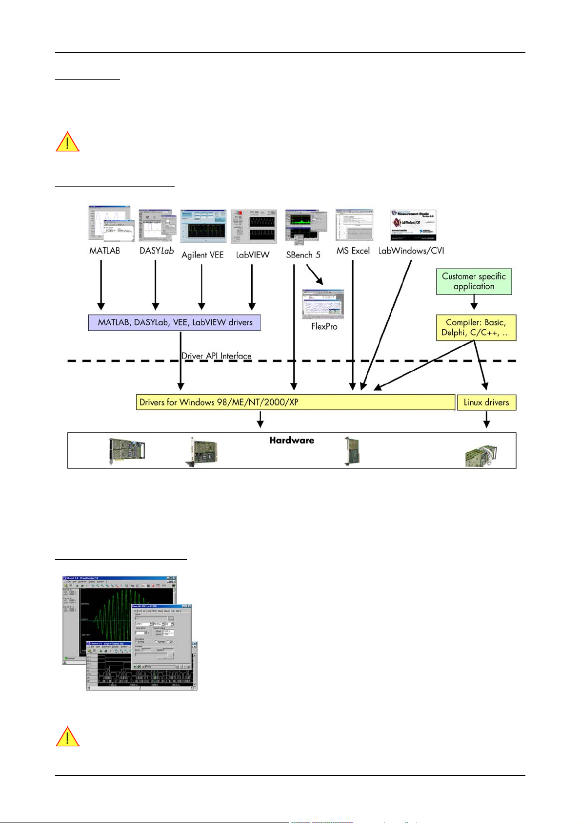
Please note that this manual provides no description for specific driver parts such as those for LabVIEW or MATLAB. These drivers are provided by special order.
For any new information on the board as well as new available options or memory upgrades please contact our website
http://www.spectrum-instrumentation.com. You will also find the current driver package with the latest bug fixes and new features on our site.
Please read this manual carefully before you install any hardware or software. Spectrum is not responsible
for any hardware failures resulting from incorrect usage.
General Information
The MC.31xx series allows recording of up to 8 channels in the middle speed segment. Due to the proven design a wide variety of 12 bit
A/D converter boards for CompactPCI bus can be offered. These boards are available in several versions and different speed grades making
it possible for the user to find a individual solution.
These boards offer two, four or eight channels with sample rates of 1 MS/s, 10 MS/s or 25 MS/s. As an option 4 digital inputs per channel
can be recorded synchronously. The installed memory of up to 256 MSample will be used for fast data recording. It can completely be used
by the current active channels. If using slower sample rates the memory can be switched to a FIFO buffer and data will be transferred online
to the PC memory or to hard disk.
Several boards of the MC.xxxx series may be connected together by the internal standard synchronisation bus to work with the same time
base.
Application examples: Laboratory equipment, Super-sonics, LDA/PDA, Radar, Spectroscopy.
6 MC.31xx Manual
Page 7
Introduction Different models of the MC.31xx series
Different models of the MC.31xx series
The following overview shows the different available models of the MC.31xx series. They differ in the number of mounted acquisition modules
and the number of available channels. You can also see the model dependant allocation of the input connectors.
• MC.3110
• MC.3120
• MC.3130
• MC.3111
• MC.3121
• MC.3131
(c) Spectrum GmbH 7
Page 8

Different models of the MC.31xx series Introduction
• MC.3112
• MC.3122
• MC.3132
8 MC.31xx Manual
Page 9
Introduction Additional options
Additional options
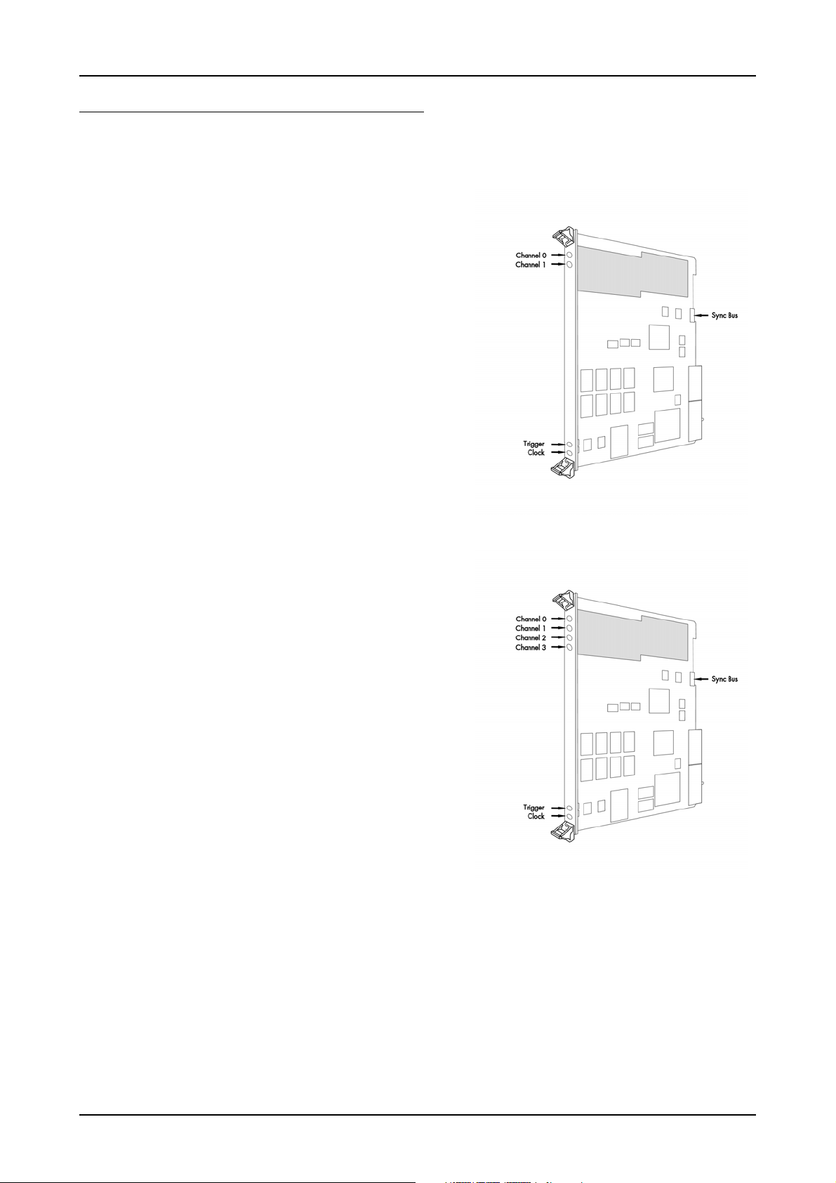
Digital inputs
This option allows the user to acquire additional digital channels synchronous and
phase-stable along with the analog data.
Therefore the analog data is filled up with the digital bits up to 16 Bit data width. This
leads to a possibility of acquiring 4 additional digital bits per channel with 12 bit resolution boards, and 2 additional digital bits per channel with 14 bit resolution boards.
The connectors for these digital inputs are mounted on an additional bracket. The figures show the option on boards with either one or two modules.
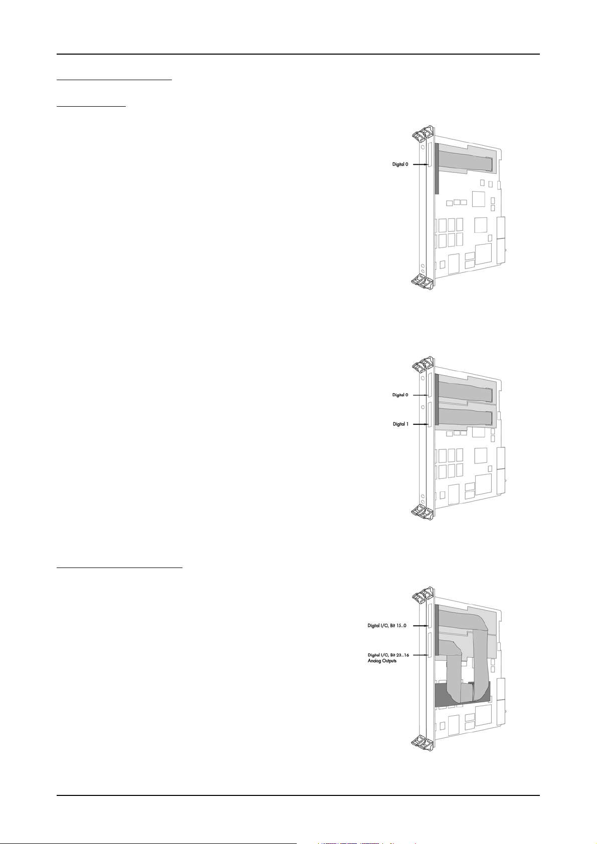
Extra I/O (Option -XMF)
With this simple-to-use enhancement it is possible to control a wide range of external
instruments or other equipment. Therefore you have 24 digital I/O and the 4 analog
outputs available.
The extra I/O option is useful if an external amplifier should be controlled, any kind
of signal source must be programmed, an antenna must be adjusted, a status information from external machine has to be obtained or different test signals have to be routed to the board.
The additional inputs and outputs are mounted on an extra bracket. The figure shows
the allocation of the two connectors. The shown option is mounted exemplarily on a
board with two modules. Of course you can also combine this option as well with a
board that is equipped with only one module.
It is not possible to use this option together with the star hub or timestamp option, because there is just space for one piggyback module on
the on-board expansion slot.
(c) Spectrum GmbH 9
Page 10
Additional options Introduction
Starhub
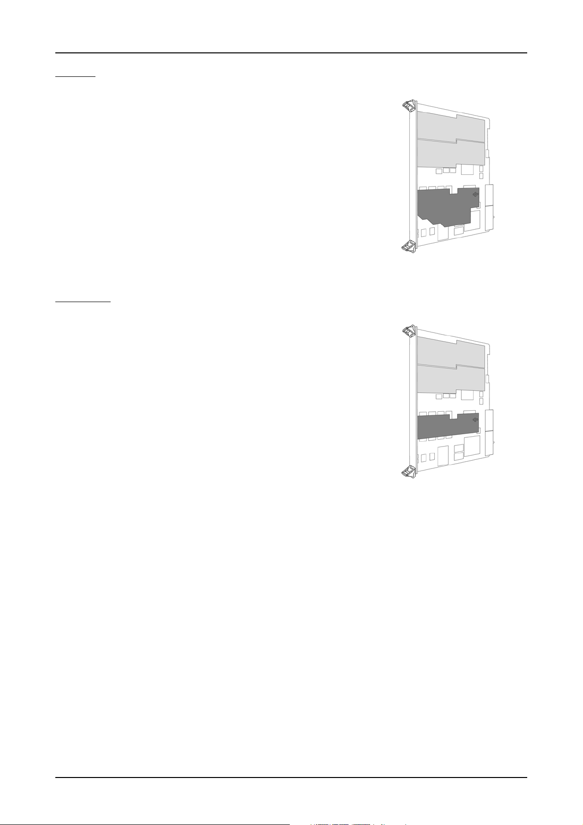
The star hub module allows the synchronisation of up to 16 MC boards. It is possible
to synchronise boards of the same type with each other as well as different types.
The module acts as a star hub for clock and trigger signals. Each board is connected
with a small cable of the same length, even the master board. That minimises the clock
skew between the different boards. The figure shows the piggyback module mounted
on the base board schematically without any cables to achieve a better visibility.
Any board could be the clock master and the same or any other board could be the
trigger master. All trigger modes that are available on the master board are also available if the synchronisation star hub is used.
The cable connection of the boards is automatically recognised and checked by the
driver at load time. So no care must be taken on how to cable the boards. The programming of the star hub is included in the standard board interface and consists of
only 3 additional commands.
It is not possible to use this option together with the timestamp or extra
I/O option, because the is just space for one piggyback module on the
on-board expansion slot.
Timestamp
The timestamp module was designed to record the exact time information between trigger events.
The timestamp reset command sets an internal counter to zero. The counter is running
with the same resolution as the sample rate. On each trigger event a timestamp is recorded in an extra FIFO. The recorded timestamps are read out asynchronously to the
board sampling.
If the absolute time information is of interest it is possible to synchronise the timestamp
counter with a 1 Hz "seconds" signal of a radio clock or a GPS receiver. In that case
the 64 bit timestamp information is split up in two parts. The one part counts the
number of seconds starting with the reset command, the other part is set to zero on
every rising edge of the seconds signal and specifies the exact time position in relation
to the seconds signal.
The figure shows the piggyback module installed on the on-board expansion slot. The
shown option is mounted exemplarily on a board with two modules.
It is not possible to use this option together with the star hub or extra
I/O option, because the is just space for one piggyback module on the
on-board expansion slot.
10 MC.31xx Manual
Page 11
Introduction The Spectrum type plate
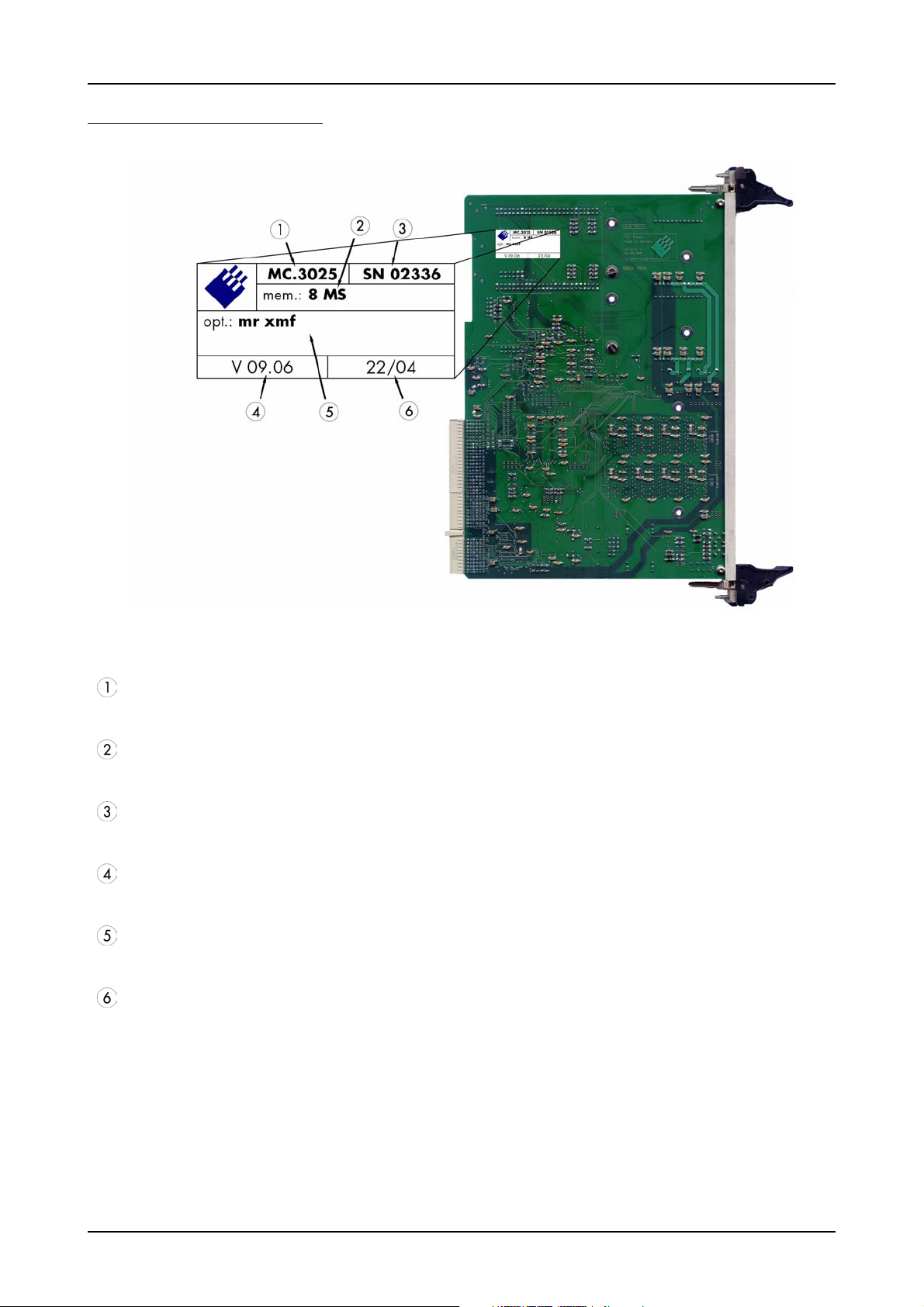
The Spectrum type plate
The Spectrum type plate, which consists of the following components, can be found on all of our boards.
The board type, consisting of the two letters describing the bus (in this case MC for the CompactPCI bus) and the model number.
The size of the on-board installed memory in MSamples. In this example there are 8 MS (16 MByte) installed.
The serial number of your Spectrum board. Every board has a unique serial number.
The board revision, consisting of the base version and the module version.
A list of the installed options. A complete list of all available options is shown in the order information. In this example the options
’Multiple recording’ and ’Extra I/O with external outputs’ are installed.
The date of production, consisting of the calendar week and the year.
Please always supply us with the above information, especially the serial number in case of support request. That
allows us to answer your questions as soon as possible. Thank you.
(c) Spectrum GmbH 11
Page 12
Hardware information Introduction
Hardware information
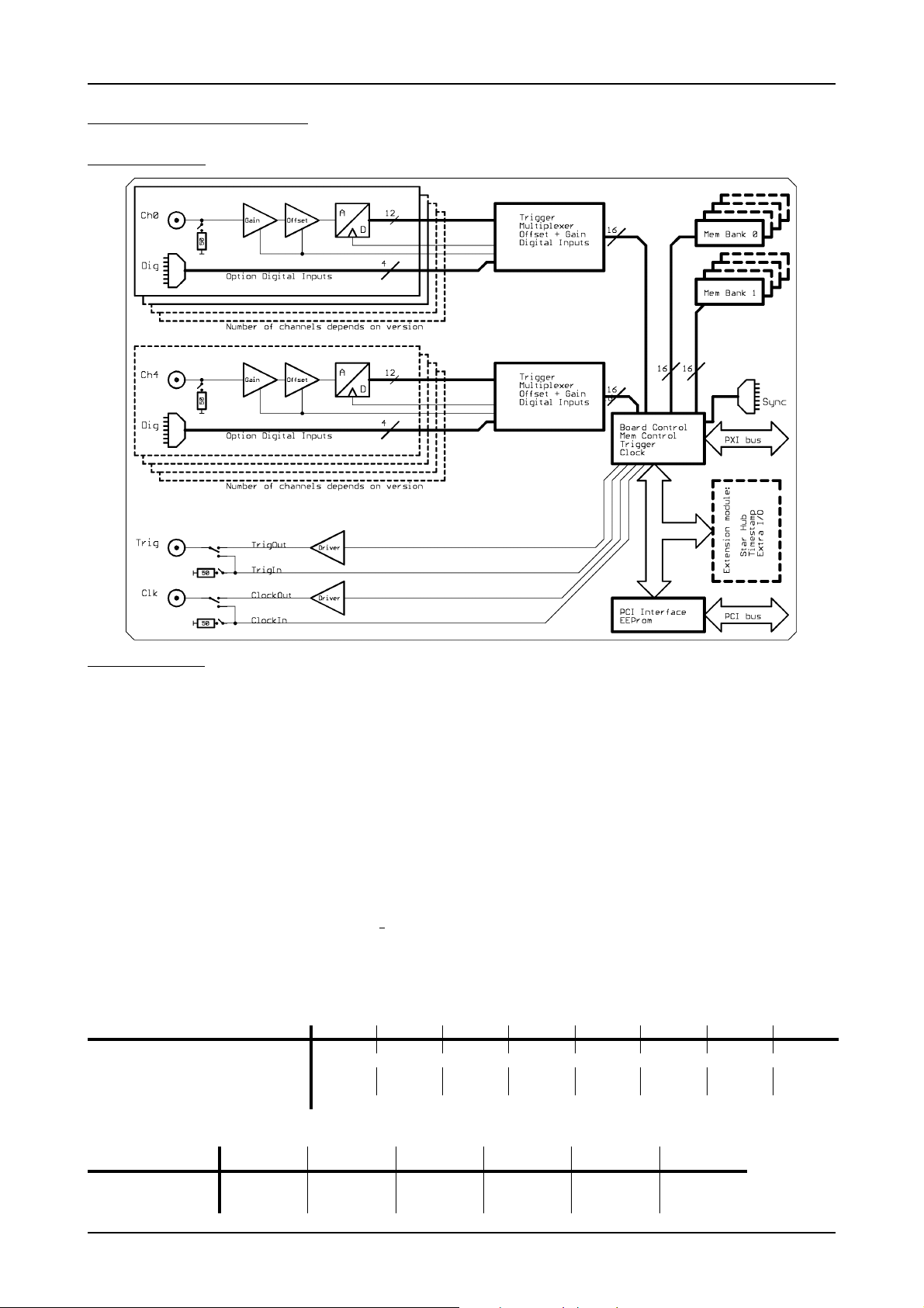
Block diagram
Technical Data
Resolution 12 bit Dimension 160 x 233 mm (Standard 6U)
Differential linearity error ≤ 1 LSB (ADC) Width (Standard) 1 slot
Integral linearity error ≤ 2.5 LSB (ADC) Width (with digital inputs) 2 slots
Multi: Trigger to 1st sample delay fix Connector 3 mm SMB male
Multi: Recovery time < 20 samples Input impedance 50 Ohm / 1 MOhm || 25 pF
ext. Trigger accuracy 1 Samples Overvoltage protection (range ≤ ±1 V) ±5 V
int. Trigger accuracy 1 Sample Overvoltage protection (range > ±1 V) ±50 V
Ext. clock: delay to internal clock 42 ns ±2 ns Warm up time 10 minutes
input signal with 50 ohm termination max 5 V rms Operating temperature 0°C - 50°C
Digital Inputs input impedance 110 Ohm @ 2.5 V Storage temperature -10°C - 70°C
Digital Inputs delay to analog sample -4 samples Humidity 10% to 90%
Min internal clock 1 kS/s
Min external clock 1 kS/s Power consumption 5 V @ full speed max. 3.3 A (16.5 Watt)
Trigger input:Standard TTL level Low: -0.5 > level < 0.8 V
Trigger output Standard TTL, capable of driving 50 Ohm.
Input range ±50 mV ±100 mV ±200 mV ±500 mV ±1 V ±2 V ±5 V ±10 V
Software programmable offset ±50 mV ±100 mV ±200 mV ±500 mV ±1 V ±2 V ±5 V ±10 V
Offset error < 1 LSB, adjustable by user
Gain error < 1 %< 1 %< 1 %< 1 %< 1 %< 1 %< 1 %< 1 %
Noise (rms): 50 Ohm, 25 MS/s < 1.5 LSB < 1.2 LSB < 1.0 LSB < 1.0 LSB < 1.0 LSB < 1.0 LSB < 1.0 LSB < 1.0 LSB
Crosstalk 500 kHz signal, ±50 mV input, 50 Ohm < -70 dB
High: 2.0 V > level < 5.5 V
Trigger pulse must be valid > 2 clock periods.
Low < 0.4 V (@ 20 mA, max 64 mA)
High > 2.4 V (@ -20 mA, max -48 mA)
One positive edge after the first internal trigger
Power consumption 5 V @ power down max. 2.5 A (12.5 Watt)
Clock input: Standard TTL level Low: -0.5 V > level < 0.8 V
Clock output Standard TTL, capable of driving 50 Ohm
High: 2.0 V > level < 5.5 V
Rising edge. Duty cycle: 50% ± 5%
Low < 0.4 V (@ 20 mA, max 64 mA)
High > 2.4 V (@ -20 mA, max -48 mA)
MC.3110
max internal clock 1 MS/s 1 MS/s 10 MS/s 10 MS/s 25 MS/s 25 MS/s
max external clock 1 MS/s 1 MS/s 10 MS/s 10 MS/s 25 MS/s 25 MS/s
-3 dB bandwidth > 500 kHz > 500 kHz > 5 MHz > 5 MHz > 12.5 MHz > 12.5 MHz
MC.3111
MC.3112 MC.3120
MC.3121
MC.3122 MC.3130
MC.3131
MC.3132
12 MC.31xx Manual
Page 13

Introduction Hardware information
Dynamic Parameters
MC.3110
Test - Samplerate 1 MS/s 1 MS/s 10 MS/s 10 MS/s 25 MS/s 25 MS/s
Testsignal frequency 90 kHz 90 kHz 1 MHz 1 MHz 1 MHz 1 MHz
SNR (typ) > 67.5 dB > 66.9 dB > 64.9 dB > 64.9 dB > 63.1 dB > 62.4 dB
THD (typ) < -62.8 dB < -62.8 dB < -62.5 dB < -62.5 dB < -62.5 dB < -62.5 dB
SFDR (typ), excl harm. > 80.8 dB > 80.5 dB > 80.5 dB > 78.5 dB > 79.5 dB > 79.3 dB
SINAD (typ) > 61.5 dB > 61.4 dB > 60.5 dB > 60.5 dB > 59.8 dB > 59.4 dB
ENOB (based on SINAD) > 9.9 LSB > 9.9 LSB > 9.8 LSB > 9.8 LSB > 9.6 LSB > 9.6 LSB
Dynamic parameters are measured at ± 1 V input range (if no other range is stated) and 50 Ohm termination with the samplerate specified in the table. Measured parameters are averaged 20 times to get typical values. Test signal is a pure sine wave of the specified frequency with > 99% amplitude. SNR and RMS noise parameters may differ depending on the quality
of the used PC. SNR = Signal to Noise Ratio, THD = Total Harmonic Distortion, SFDR = Spurious Free Dynamic Range, SINAD = Signal Noise and Distortion, ENOB = Effective Number
of Bits. For a detailed description please see application note 002.
MC.3111
MC.3112 MC.3120
MC.3121
MC.3122 MC.3130
MC.3131
MC.3132
Order information
Order No Description Order No Description
MC3110 MC.3110 with 8 MSample memory and drivers/SBench 5.x MC3xxx-16M Option: 16 MSample memory instead of 8 MSample standard mem
MC3111 MC.3111 with 8 MSample memory and drivers/SBench 5.x MC3xxx-32M Option: 32 MSample memory instead of 8 MSample standard mem
MC3112 MC.3112 with 8 MSample memory and drivers/SBench 5.x MC3xxx-64M Option: 64 MSample memory instead of 8 MSample standard mem
MC3120 MC.3120 with 8 MSample memory and drivers/SBench 5.x MC3xxx-128M Option: 128 MSample memory instead of 8 MSample standard mem
MC3121 MC.3121 with 8 MSample memory and drivers/SBench 5.x MC3xxx-256M Option: 256 MSample memory instead of 8 MSample standard mem
MC3122 MC.3122 with 8 MSample memory and drivers/SBench 5.x MC3xxx-up Additional handling costs for later memory upgrade
MC3130 MC.3130 with 8 MSample memory and drivers/SBench 5.x
MC3131 MC.3131 with 8 MSample memory and drivers/SBench 5.x MC3xxx-mr Option Multiple Recording: Memory segmentation
MC3132 MC.3132 with 8 MSample memory and drivers/SBench 5.x MC3xxx-gs Option Gated Sampling: Gate signal controls acquisition
MC3xxx-smod Star Hub: Synchronisation of 2 - 16 boards, one option per system
MC3xxx-time Timestamp option: Extra memory for trigger time MC31xx-dl DASYLab driver for MC.31xx series
MCxxxx-xmf Extra I/O, external connector: 24 DI/O, 4 Analog out, incl. cable MC31xx-hp VEE driver for MC.31xx series
MC3xxx-cs Synchronisation of 2 - 4 boards, one option per system MATLAB MATLAB driver for all MI.xxxx, MC.xxxx and MX.xxxx series.
MC3xxx-dig Additional 4 synchronous digital inputs per channel, incl. cable
MC31xx-lv LabVIEW driver for MC.31xx series
Cab-3f-9m-80 Adapter cable: SMB female to BNC male 80 cm Cab-3f-9f-80 Adapter cable: SMB female to BNC female 80 cm
Cab-3f-9m-200 Adapter cable: SMB female to BNC male 200 cm Cab-3f-9f-200 Adapter cable: SMB female to BNC female 200 cm
(c) Spectrum GmbH 13
Page 14
System Requirements Hardware Installation
Hardware Installation
System Requirements
All Spectrum MC.xxxx instrumentation boards are compliant to the CompactPCI 6U standard and require in general one free slot. Depending
on the installed options additional free slots can be necessary.
Warnings
ESD Precautions
The boards of the MC.xxxx series contain electronic components that can be damaged by electrostatic discharge (ESD).
Before installing the board in your system or even before touching it, it is absolutely necessary to bleed of
any electrostatic electricity.
Cooling Precautions
The boards of the MC.xxxx series operate with components having very high power consumption at high speeds. For this reason it is absolutely required to cool this board sufficiently. It is strongly recommended to install an additional cooling fan producing a stream of air across
the boards surface. In most cases CompactPCI systems are already equipped with sufficient cooling power. In that case please make sure
that the air stream is not blocked.
During longer pauses between the single measurements the power down mode should be called to reduce the heat production.
Sources of noise
The boards of the MC.xxxx series should be placed far away from any noise producing source (like e.g. the power supply). It should especially be avoided to place the board in the slot directly adjacent to another fast board (like the graphics controller).
Installing the board in the system
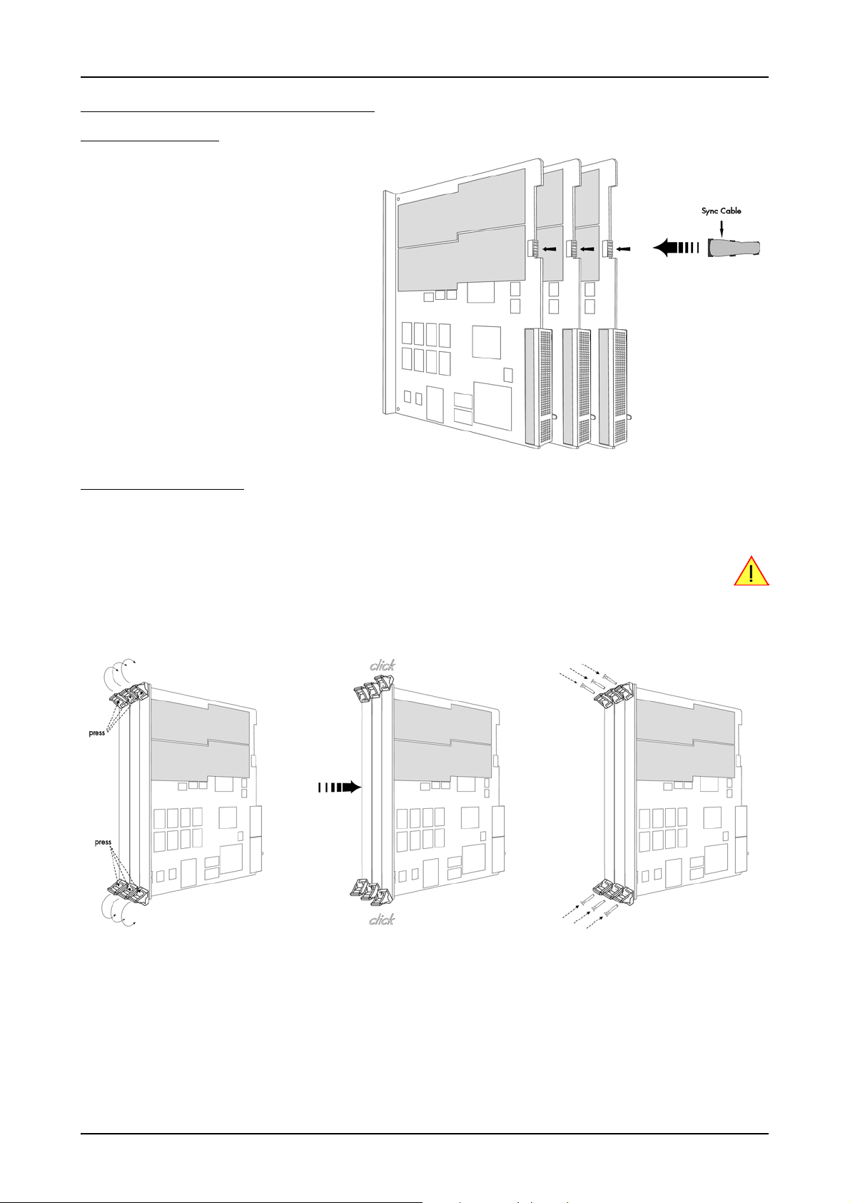
Installing a single board without any options
The locks on the top and bottom side of CompactPCI boards need to be unlocked and opened before installing the board into a free slot of
the system. Therefore you need to press the little buttons on the inside of the fasteners and move them outwards (see figure). Now slowly insert
the card into the host system using the key ways until both locks snap in with a „click“.
While inserting the board take care not to tilt it.
After the board’s insertion fasten the two screws carefully, without overdoing.
14 MC.31xx Manual
Page 15
Hardware Installation Installing the board in the system
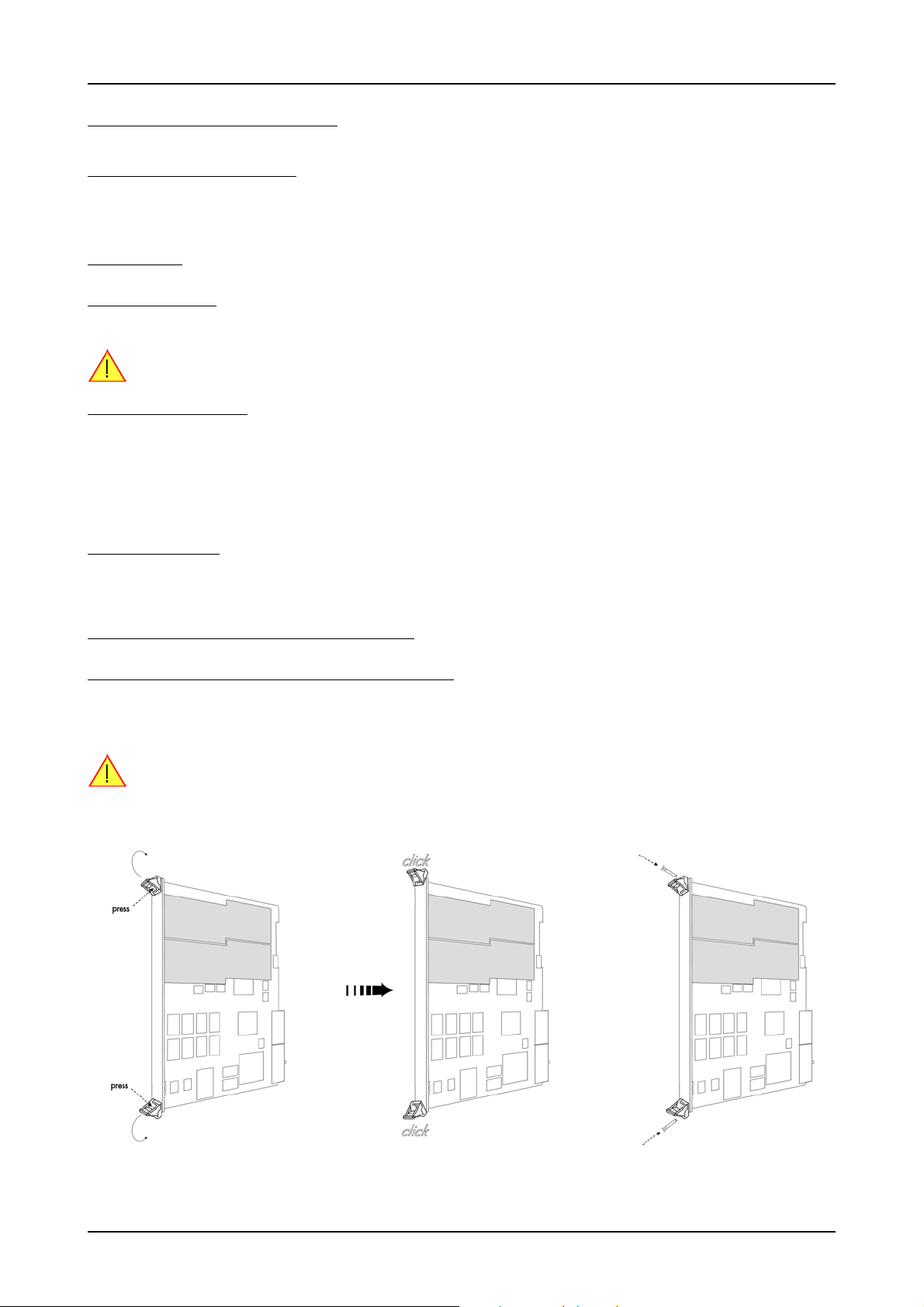
Installing a board with digital inputs/outputs
The locks on the top and bottom side of both CompactPCI brackets need to be unlocked and opened before installing the board into a free
slot of the system. Therefore you need to press the little buttons on the inside of the fasteners and move them outwards (see figure). Now slowly
insert the card into the host system using the key ways until both locks snap in with a „click“.
While inserting the board take care not to tilt it.
After the board’s insertion fasten the four screws of both brackets carefully, without overdoing. The figure shows an example of a board with
two installed modules.
Installing a board with extra I/O (Option -XMF)
The locks on the top and bottom side of both CompactPCI brackets need to be unlocked and opened before installing the board into a free
slot of the system. Therefore you need to press the little buttons on the inside of the fasteners and move them outwards (see figure). Now slowly
insert the card into the host system using the key ways until both locks snap in with a „click“.
While inserting the board take care not to tilt it.
After the board’s insertion fasten the four screws of both brackets carefully, without overdoing. The figure shows exemplarily a board with
two installed modules.
(c) Spectrum GmbH 15
Page 16
Installing the board in the system Hardware Installation
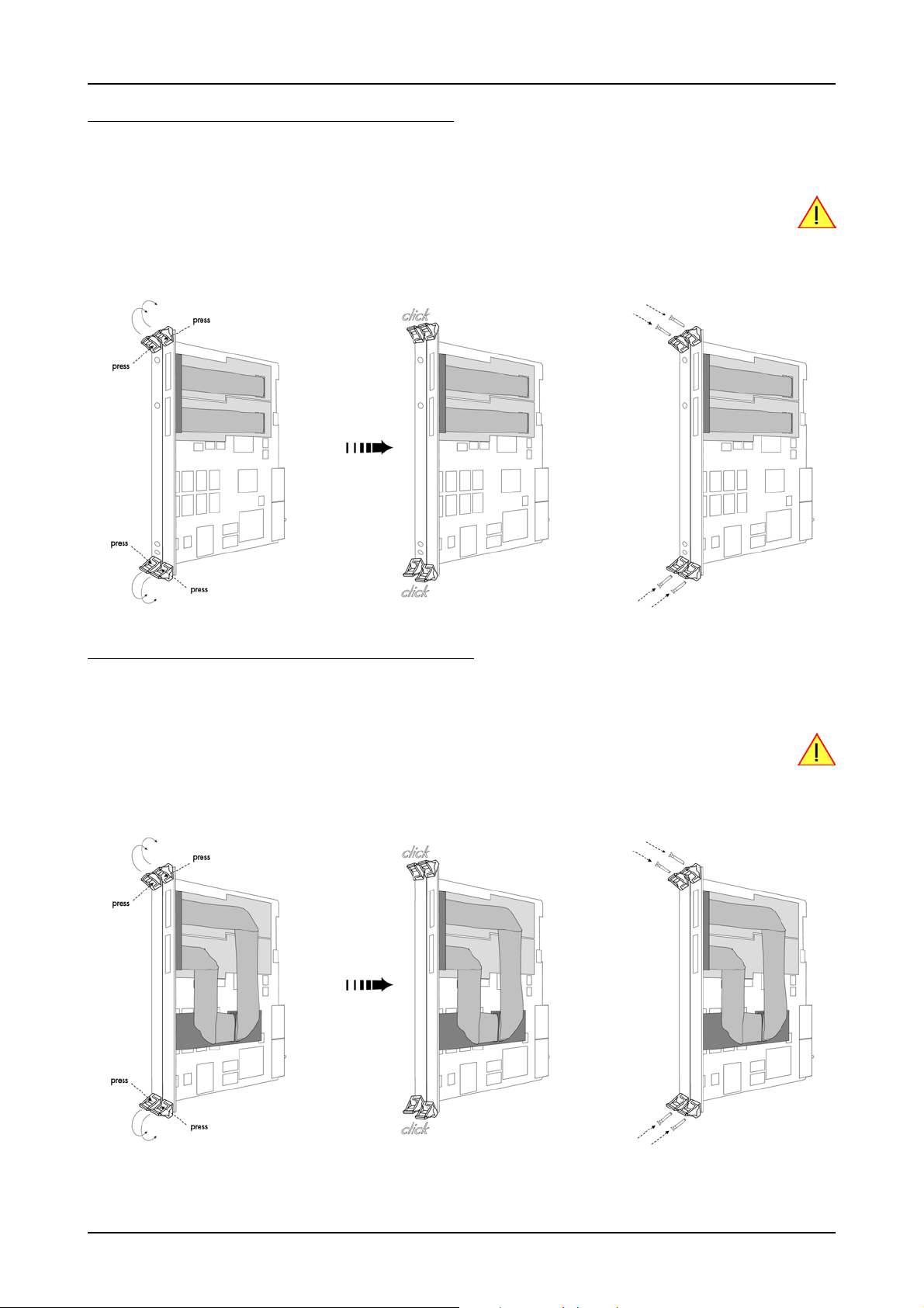
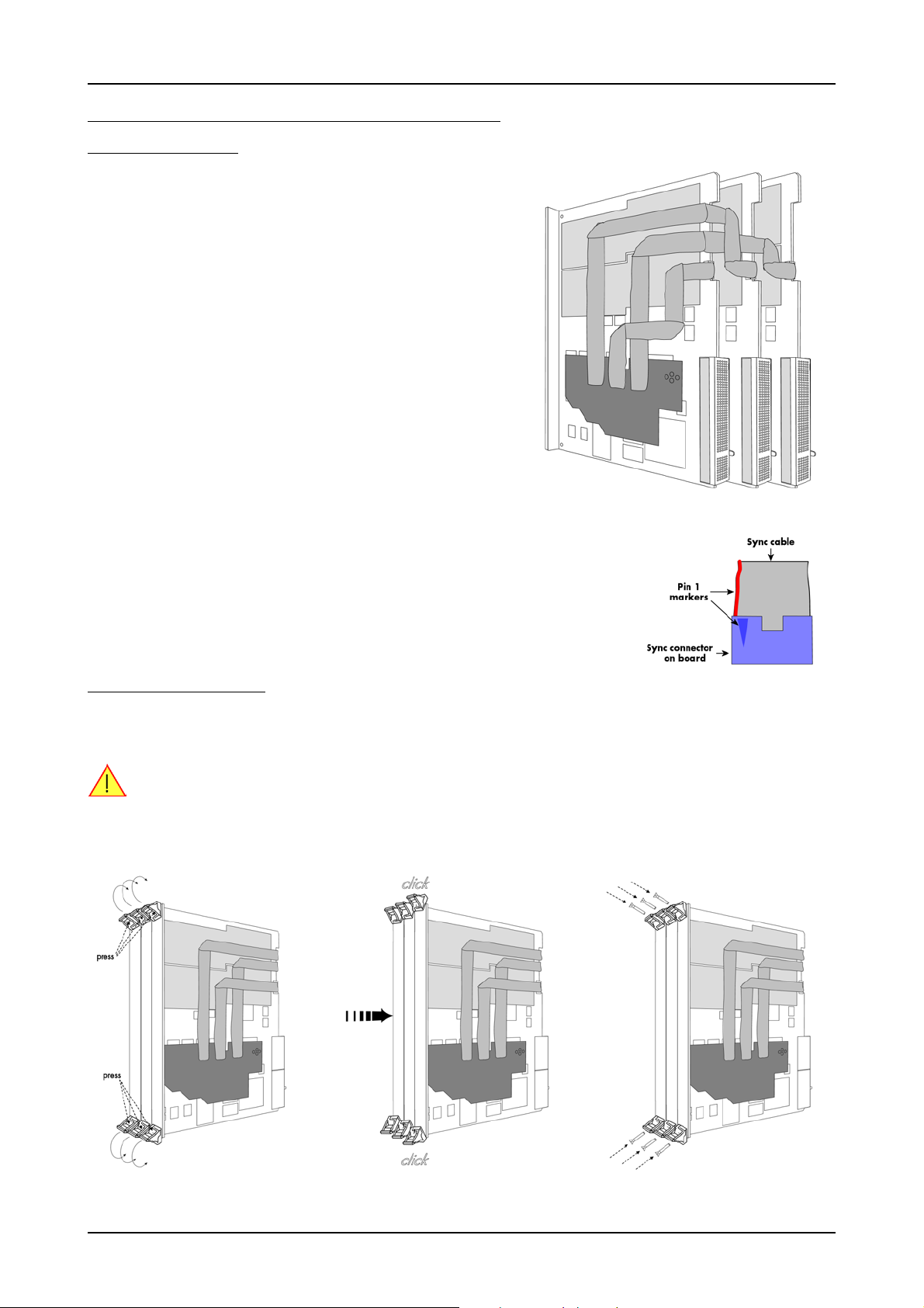
Installing multiple boards synchronized by starhub
Hooking up the boards
Before mounting several synchronized boards for a multi channel system into the
chassis you have to hook up the boards with their synchronization cables first.
Spectrum ships the boards together with the needed amount of synchronization cables. All of them are matched to the same length, to achieve a zero clock delay
between the boards.
Only use the included flat ribbon cables.
All of the boards, including the board that carrys the starhub piggy-back module,
must be wired to the starhub as the figure is showing exemplarily for three synchronized boards.
As you can see, all boards have a notch to get the cables to the other boards.
Please only use these notches to lay the cables to avoid damage to the cables when
inserting the boards into the host system.
It does not matter which of the 16 connectors on the starhub module you use for
which board. The software driver will detect the types and order of the synchronized boards automatically. The right figure shows the three cables mounted next
to each other only to achieve a better visibility.
As some of the synchronization cables are not secured against wrong plugging you should take
care to have the pin 1 markers on the multiple connectors and the cable on the same side, as the
figure on the right is showing.
Mounting the wired boards
The locks on the top and bottom side of all CompactPCI brackets need to be unlocked and opened before installing the boards into the slots
of the system. Therefore you need to press the little buttons on the inside of the fasteners and move them outwards (see figure). Now slowly
insert the boards into the host system using the key ways until both locks snap in with a „click“.
While inserting the boards take care not to cant them and make sure that the cables are not squeezed by the
backplane or any other components.
After the board’s insertion fasten the screws of all brackets carefully, without overdoing. The figure shows exemplarily a board with two installed modules.
16 MC.31xx Manual
Page 17
Hardware Installation Installing the board in the system
Installing multiple synchronized boards
Hooking up the boards
Before mounting several synchronized boards for a multi
channel system into the chassis you have to hook up the
boards with their syncronization cables first. Spectrum
ships the boards together with the needed synchronization
cable.
All of the possible four boards must be wired with delivered synchronization cable. The figure is showing that exemplarily for three synchronized boards. As you can see,
all boards have a notch to get the cables from one board
to the other. Please take care that the cable lays within
these notches to avoid damages to the cable when inserting the boards into the host system.
The outer boards have a soldered termination for the sync
bus. These boards are marked with an additional sticker.
Only mount the cluster of synchronized boards
in a row with the dedicated boards on the outer
sides.
Mounting the wired boards
The locks on the top and bottom side of all CompactPCI brackets need to be unlocked and opened before installing the boards into the slots
of the system. Therefore you need to press the little buttons on the inside of the fasteners and move them outwards (see figure). Now slowly
insert the boards into the host system using the key ways until both locks snap in with a „click“.
While inserting the boards take care not to cant them and make sure that the cable is not squeezed by the
backplane or any other components.
After the board’s insertion fasten the screws of all brackets carefully, without overdoing. The figure shows exemplarily a board with two installed modules.
(c) Spectrum GmbH 17
Page 18

Interrupt Sharing Software Driver Installation
Software Driver Installation
Before using the board a driver must be installed that matches the operating system. The installation is done in different ways depending on
the used operating system. The driver that is on CD supports all boards of the MI, MC and MX series. That means that you can use the same
driver for all boards of theses families.
Interrupt Sharing
This board uses a PCI interrupt for DMA data transfer and for controlling the FIFO mode. The used interrupt line is allocated by the PC BIOS
at system start and is normally depending on the selected slot. Because there is only a limited number of interrupt lines available on the PCI
bus it can happen that two or more boards must use the same interrupt line. This so called interrupt sharing must be supported by all drivers
of the participating equipment.
Most available drivers and also the Spectrum driver for your board can manage interrupt sharing. But there are also some drivers on the
market that can only use one interrupt exclusively. If this equipment shares an interrupt with the Spectrum board, the system will hang up if
the second driver is loaded (the time is depending on the operating system).
If this happens it is necessary to reconfigure the system in that way that the critical equipment has an exclusive access to an interrupt.
On most systems the BIOS shows a list of all installed PCI boards with their allocated interrupt lines directly after system start. You have to
check whether an interrupt line is shared between two boards. Some BIOS allow the manual allocation of interrupt lines. Have a look in your
mainboard manual for further information on this topic.
Because normally the interrupt line is fixed for one PCI slot it is simply necessary to use another slot for the critical board to force a new
interrupt allocation. You have to search a configuration where all critical boards have only exclusive access to one interrupt.
Depending on the system, using the Spectrum board with a shared interrupt may degrade performance a little. Each interrupt needs to be
checked by two drivers. For this reason when using time critical FIFO mode even the Spectrum board should have an exclusively access to
one interrupt line.
18 MC.31xx Manual
Page 19
Software Driver Installation Windows 98
Windows 98
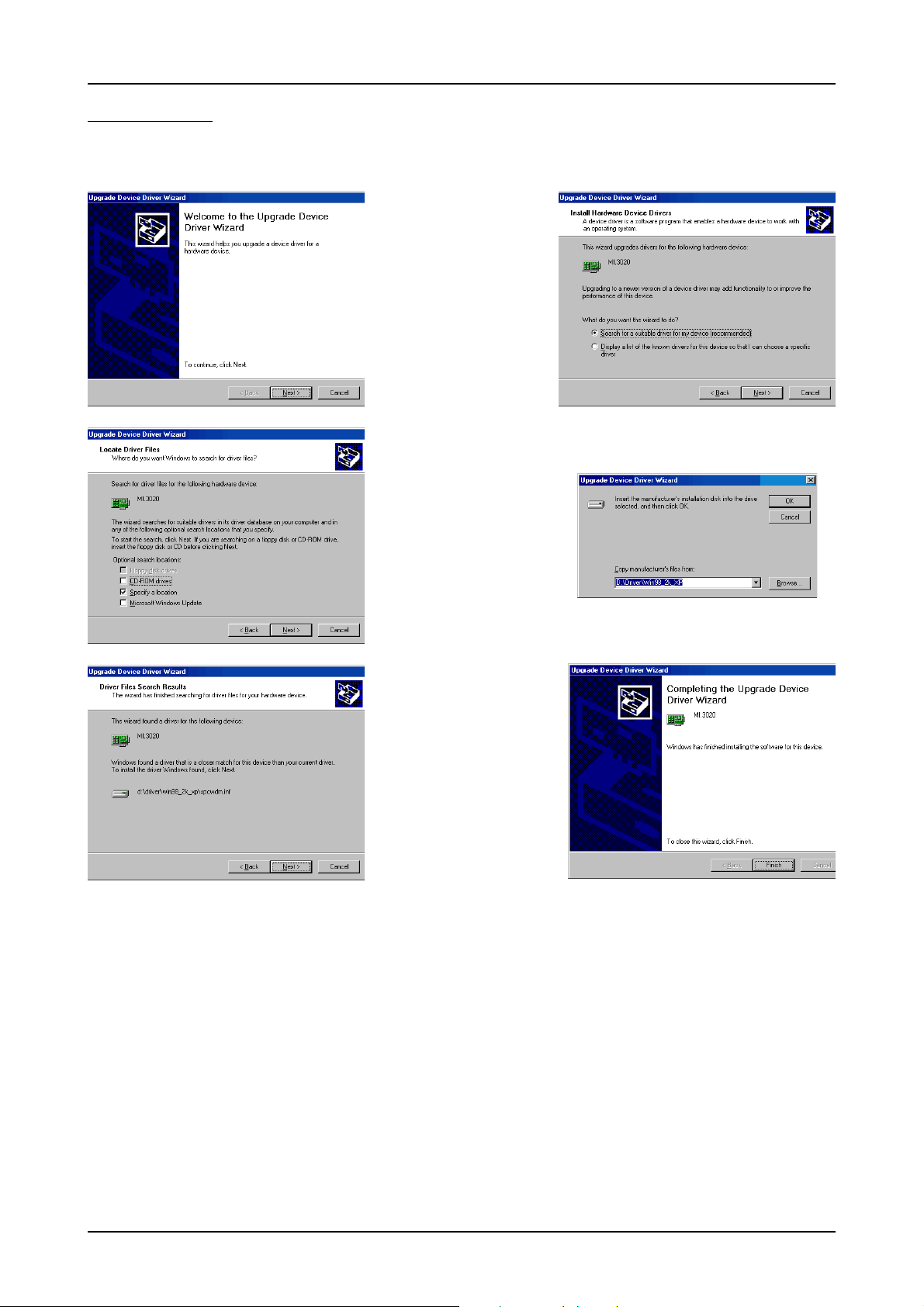
Installation
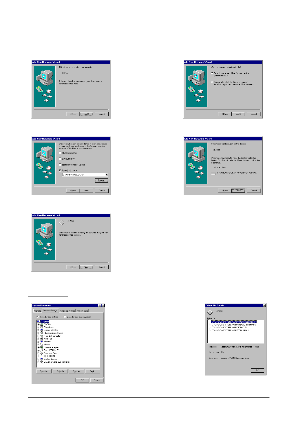
When installing the board in a Windows 98 system the Spectrum board
will be recognized automatically on
the next start-up.
The system offers the direct installation of a driver for the board.
Let Windows search automatically
for the best driver for your system.
Select the CD that was delivered
with the board as installation source.
The driver files are located on CD in
the directory
\Driver\Win98_2k_XP.
The hardware assistant shows you
the exact board type that has been
found like the MI.3020 in the example. Older boards (before june
2004) show „Spectrum Board“ instead.
Version control
The drivers can be used directly after installation. It is not necessary to restart the system.
The installed drivers are linked in the device manager. Below you’ll see how to examine
the driver version and how to update the driver with a newer version.
If you want to check which driver version is installed
in the system this can be easily done in the device
manager. Therefore please start the device manager
from the control panel and show the properties of the
installed driver.
On the property page Windows 98 shows the date
of the driver.
(c) Spectrum GmbH 19
Page 20
Windows 98 Software Driver Installation
After clicking the driver info button the detailed version information of the driver is shown. In the case
of a support question this information must be presented together with the board’s serial number to
the support team to help finding a fast solution.
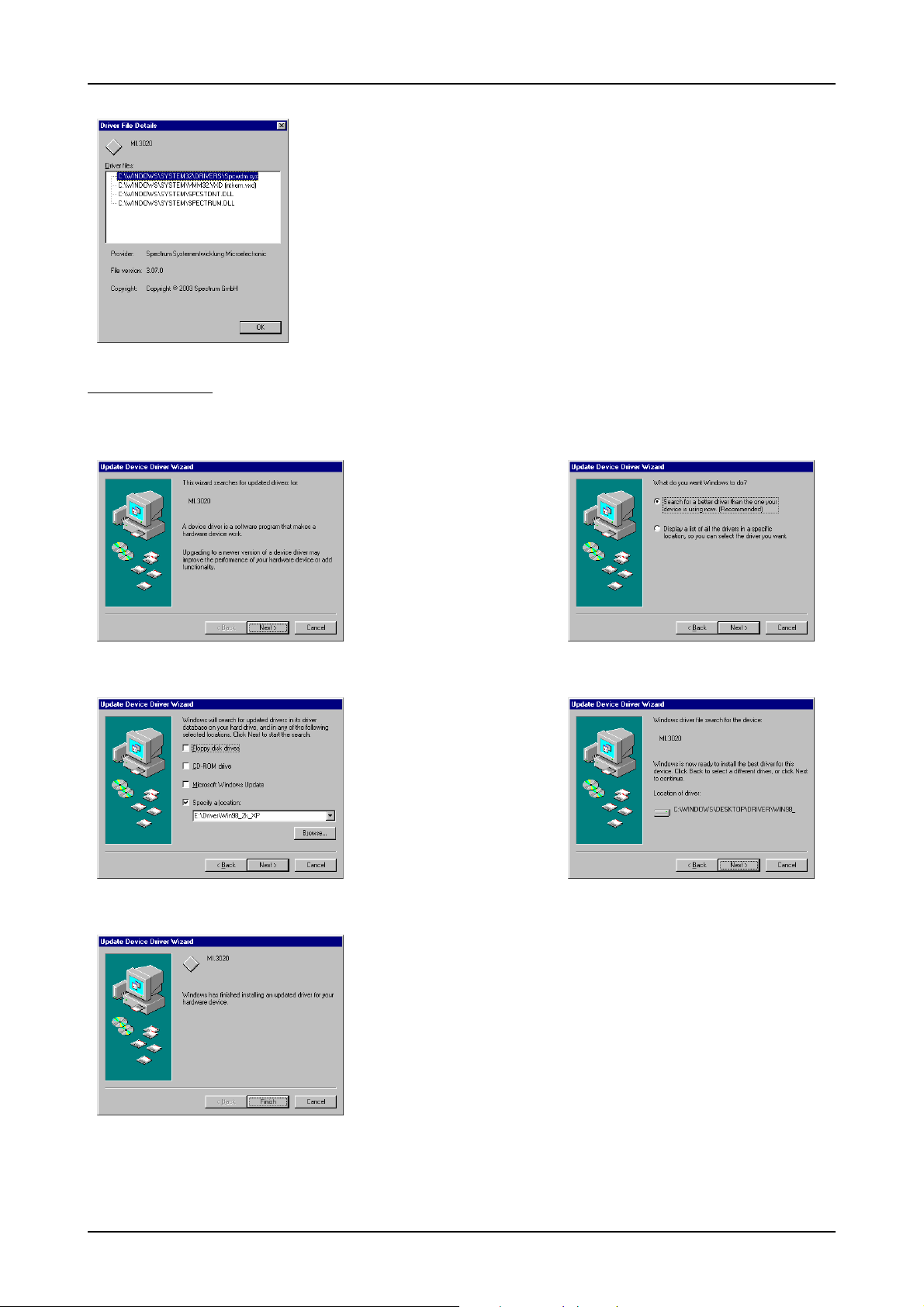
Driver - Update
If a new driver version is to be installed no Spectrum board should be in use. So please stop and exit all software that could access the boards.
New drivers are available at http://www.spectrum-instrumentation.com. After down loading the driver unzip it to a temporary folder.
A new driver version is directly installed from the device manager.
Therefore please open the properties
page of the driver as shown in the
section before. As next step click on
the update driver button and follow
the steps of the driver installation in
a similar way to the previous board
and driver installation.
Please select the path where the new
driver version was unzipped to. If
you’ve got the new driver version on
CD please select the
\Driver\Win98_2k_XP path on the
CD containing the new driver version.
The new driver version can be used directly after installation without restarting the system.
Please keep in mind to update the driver of all installed Spectrum boards.
20 MC.31xx Manual
Page 21
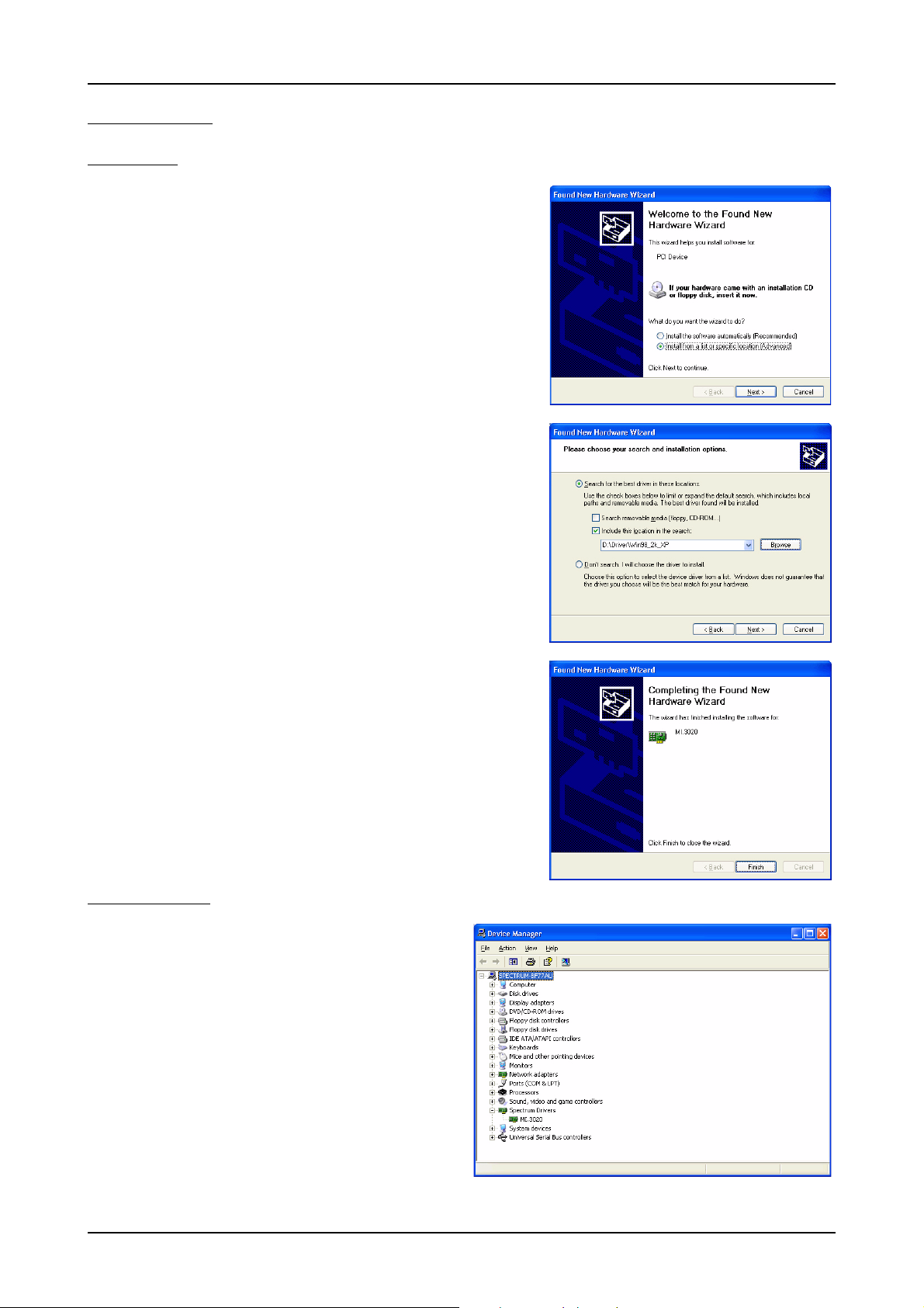
Software Driver Installation Windows 2000
Windows 2000
Installation
When installing the board in
a Windows 2000 system the
Spectrum board will be recognized automatically on the
next start-up.
The system offers the direct installation of a driver for the
board.
Let Windows search automatically for the best driver for
your system.
Select the CD that was delivered with the board as installation source. The driver files
are located on CD in the directory
\Driver\Win98_2k_XP.
Version control
The hardware assistant
shows you the exact board
type that has been found like
the MI.3020 in the example.
Older boards (before june
2004) show „Spectrum
Board“ instead.
The drivers can be used directly after installation. It is
not necessary to restart the
system. The installed drivers
are linked in the device manager.
Below you’ll see how to examine the driver version and
how to update the driver with
a newer version.
If you want to check which driver version
is installed in the system this can be easily done in the device manager. Therefore please start the device manager
from the control panel and show the
properties of the installed driver.
On the property page Windows 2000
shows the date and the version of the installed driver.
After clicking the driver details button the
detailed version information of the driver
is shown. In the case of a support question this information must be presented
together with the board’s serial number
to the support team to help finding a fast
solution.
(c) Spectrum GmbH 21
Page 22
Windows 2000 Software Driver Installation
Driver - Update
If a new driver version should be installed no Spectrum board is allowed to be in use by any software. So please stop and exit all software
that could access the boards.
A new driver version is directly installed from the device
manager. Therefore please
open the properties page of
the driver as shown in the section before. As next step click
on the update driver button
and follow the steps of the
driver installation in a similar
way to the previous board
and driver installation.
Please select the path where
the new driver version was
unzipped to. If you’ve got the
new driver version on CD
please select the
\Driver\Win98_2k_XP path
on the CD containing the new
driver version.
The new driver version can
be used directly after installation without restarting the system. Please keep in mind to
update the driver of all installed Spectrum boards.
22 MC.31xx Manual
Page 23
Software Driver Installation Windows XP
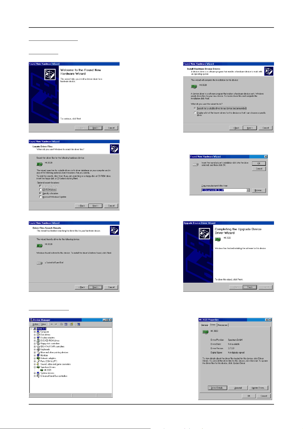
Windows XP
Installation
When installing the board in a Windows XP system the Spectrum board will be recognized automatically on the next start-up.
The system offers the direct installation of a driver for the board.
Do not let Windows automatically search for the best driver, because sometimes the driver will not be found on the CD. Please take
the option of choosing a manual installation path instead.
Allow Windows XP to search for the most suitable driver in a specific directory. Select the CD that was delivered with the board as installation source. The driver files
are located on CD in the directory \Driver\Win98_2k_XP.
The hardware assistant shows you the exact board type that has been found like
the MI.3020 in the example. Older boards (before june 2004) show „Spectrum
Board“ instead.
The drivers can be used directly after installation. It is not necessary to restart the
system. The installed drivers are linked in the device manager.
Below you’ll see how to examine the driver version and how to update the driver
with a newer version.
Version control
If you want to check which driver version is installed in the system this
can be easily done in the device manager. Therefore please start the
device manager from the control panel and show the properties of
the installed driver.
(c) Spectrum GmbH 23
Page 24
Windows XP Software Driver Installation
On the property page Windows XP shows the date and the version of the installed driver.
After clicking the driver details button the detailed version information of the driver is shown.
In the case of a support question this information must be presented together with the
board’s serial number to the support team to help finding a fast solution.
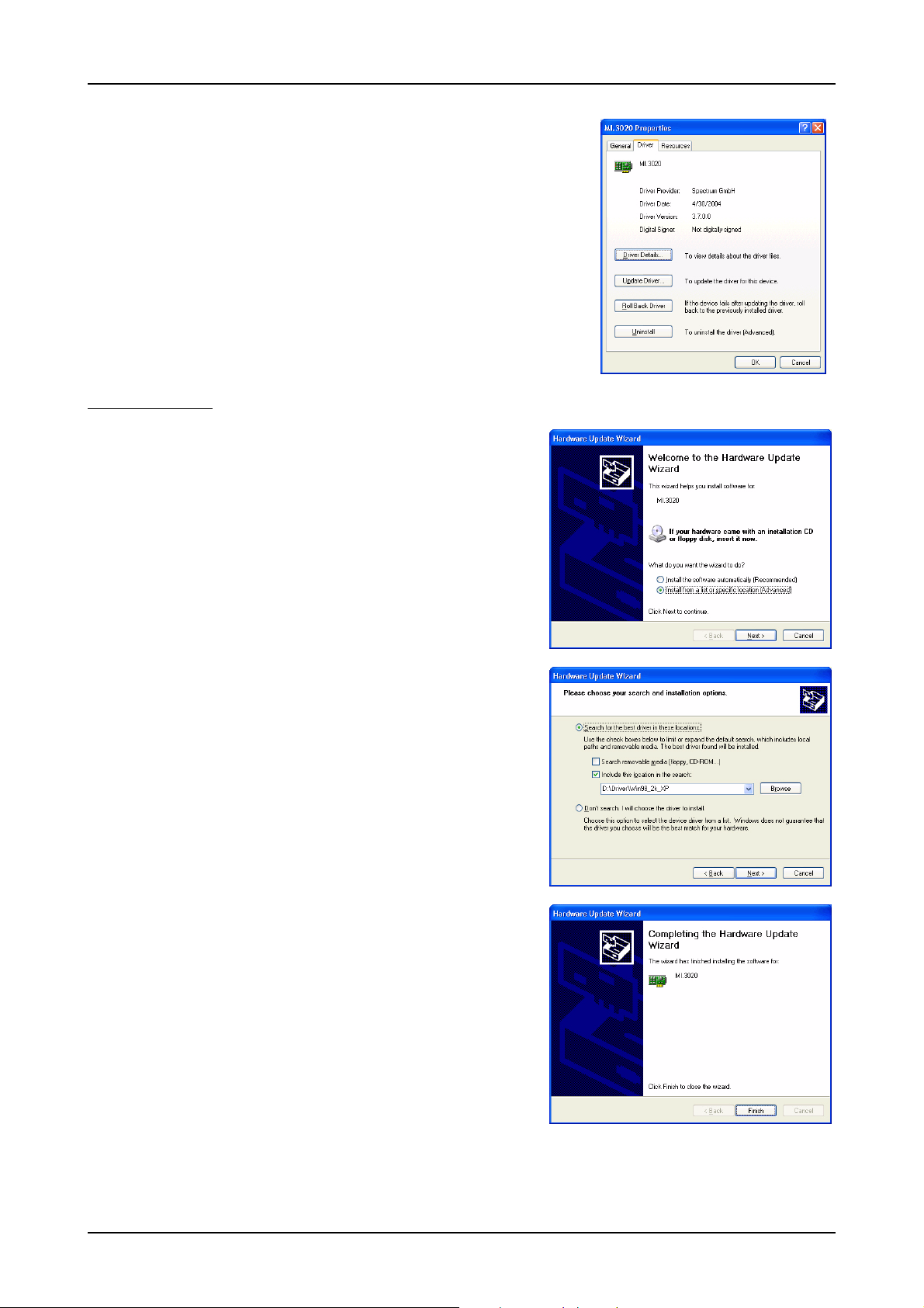
Driver - Update
If a new driver version should be installed no Spectrum board is allowed to be in
use by any software. So please stop and exit all software that could access the
boards.
A new driver version is directly installed from the device manager. Therefore please
open the properties page of the driver as shown in the section before. As next step
click on the update driver button and follow the steps of the driver installation in a
similar way to the previous board and driver installation.
Please select the path where the new driver version was unzipped to. If you’ve got
the new driver version on CD please select the \Driver\Win98_2k_XP path on the
CD containing the new driver version.
The new driver version can be used directly after installation without restarting the
system. Please keep in mind to update the driver of all installed Spectrum boards.
24 MC.31xx Manual
Page 25
Software Driver Installation Windows NT
Windows NT
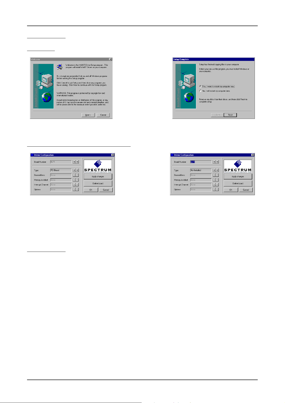
Installation
Under Windows NT the
Spectrum driver must be installed manually. The driver is
found on CD in the directory
\Install\WinNTDrv. Please
start the „Setup.exe“ program. The installation is performed totally automatically,
simply click on the „Next“
button. After installtion the
system must be rebooted
once (see picture on the right
side). The driver is install to
pactPCI device. If more boards are installed in the system the configuration of the driver has to be changed. Please see the following chapter
for this topic.
Adding boards to the Windows NT driver
support one PCI/PXI or Com-
The Windows NT driver
must be configured by the
Driver Configuration utility
to support more than one
board. The Driver Configuration utility is automatically installed with the driver.
The Utility can be found in
the start menu as „DrvConfig“.
To add a new card please follow these steps:
• Increase the board number on top of the screen by pressing the right button
• Change the board type from „Not Installed“ to „PCI Board“
• Press the „Apply changes“ button
• Press the „OK“ button
• Restart the system
Driver - Update
If a new driver version should be installed no Spectrum board is allowed to be in use by any software. So please stop and exit all software
that could access the boards.
When updating a system please simply execute the setup file of the new driver version. Afterwards the system has to be rebooted. The driver
configuration is not changed.
(c) Spectrum GmbH 25
Page 26

Linux Software Driver Installation
Linux
Overview
The Spectrum boards are delivered with drivers for linux. It is necessary to install them manually following the steps explained afterwards.
The linux drivers can be found on CD in the directory /Driver/linux. As linux is an open source operating system there are several distributions
in use world-wide that are compiled with different kernel settings. As we are not able to install and maintain hundreds of different distributions
and versions we had to focus on some common used linux distributions.
However if your distribution does not work with one of these pre-compiled kernel modules or you have a specialized kernel installed (like a
SMP kernel) you can get the linux driver sources directly from us. With this sources it’s no problem to compile and use the linux driver on your
system. Please contact your local distributor to get the sources. The Spectrum linux drivers are compatible with kernel versions 2.4 and 2.6.
On this CD you’ll find pre-compiled linux kernel modules for the following versions:
SuSE version 8.0 Kernel 2.4.18 directory /Driver/linux/suse80 SuSE version 8.2 Kernel 2.4.20 directory /Driver/linux/suse82
SuSE version 9.0 Kernel 2.4.21 directory /Driver/linux/suse90 SuSE version 9.1 Kernel 2.6.4 directory /Driver/linux/suse91
Redhat version 9.0 Kernel 2.4.20 directory /Driver/linux/redhat90
Installation
Login as root.
It is necessary to have the root rights for installing a driver.
Select the right driver from the CD.
Refer to the list shown above. If your distribution is not listed there please select the module that most closely matches your installed kernel
version. Copy the driver kernel module spc.o from the CD directory to your hard disk. Be sure to use a hard disk directory that is a accessible
by all users who should work with the board.
First time load of the driver
The linux driver is shipped as the loadable module spc.o. The driver includes all Spectrum PCI, PXI and CompactPCI boards. The boards are
recognized automatically after driver loading.Load the driver with the insmod command:
linux:~ # insmod spc.o
The insmod command may generate a warning that the driver module was compiled for another kernel version. In that case you may try to
load the driver module with the force parameter and test the board very carefully.
linux:~ # insmod -f spc.o
If the kernel module could not be loaded in your linux installation it is necessary to compile the driver directly on your system. Please contactSpectrum to get the needed source files including the compilation description.
Depending on the used linux distribution the insmod command generates a message telling the driver version and the board types and serial
numbers that have been found. If your distribution does not show this message it is possible to view them with the dmesg command:
linux:~ # dmesg
... some other stuff
spc driver version: 3.07 build 0
sp0: MI.3020 sn 01234
In the example we show you the output generated by a MI.3020. All other board types are similar to this output but showing the correct
board type.
Examine the major number of the driver
For accessing the device driver it is necessary to know the major number of the device. This number is listed in the /proc/devices list. The
device driver is called "spec" in this list. Normally this number is 254 but this depends on the device drivers that have been installed before.
linux:~ # cat /proc/devices
Character devices:
...
171 ieee1394
180 usb
188 ttyUSB
254 spec
Block devices:
1 ramdisk
2 fd
...
26 MC.31xx Manual
Page 27

Software Driver Installation Linux
Installing the device
You connect a device to the driver with the mknod command. The major number is the number of the driver as shown in the last step, the
minor number is the index of the board starting with 0. This step must only be done once for the system where the boards are installed in.
The device will remain in the file structure even if the board is de-installed from the system.
The following command makes a device for the first Spectrum board the driver has found:
linux:~ # mknod /dev/spc0 c 254 0
Make sure that the users who work with the driver have full rights access for the device. Therefore you should give all persons all rights to the
device:
linux:~ # chmod a+w /dev/spc0
Now it is possible to access the board using this device.
Driver info
Information about the installed boards could be found in the /proc/spectrum file. All PCI, PXI and CompactPCI boards show the basic information found in the EEProm there. This is an example output generated by a MI.3020:
linux:~ # cat /proc/spectrum
Spectrum driver information
--------------------------Driver Version: 3.07 build 0
Board#0: MI.3020
serial number: 01234
production month: 05/2004
version: 9.6
samplerate: 100 MHz
installed memory: 16 MBytes
Automatic load of the driver
It is necessary to load the kernel driver module after each start of the system before using the boards. Therefore you may add the „insmod
spc.o“ command in one of the start-up files. Or you may load the kernel driver module manually whenever you need access to the board.
(c) Spectrum GmbH 27
Page 28
Software Overview Software
Software
This chapter gives you an overview about the structure of the drivers and the software, where to find and how to use the examples. It detailed
shows how the drivers are included under different programming languages and where the differences are when calling the driver functions
from different programming languages.
This manual only shows the use of the standard driver API. For further information on programming drivers
for third-party software like LabVIEW, MATLAB, DASYLab or VEE an additional manual is required that is delivered with the ordered driver option.
Software Overview
The Spectrum drivers offer you a common and fast API for using all of the board hardware features. This API is nearly the same on all operating
systems. Based on this API one can write your own programs using any programming language that can access the driver API. This manual
detailed describes the driver API allowing you to write your own programs.
The optional drivers for third-party products like LabVIEW or DASYLab are also based on this API. The special functionality of these drivers
is not subject of this manual and is described on separate manuals delivered with the driver option.
First Test with SBench
After installation of the board and the drivers it can be useful to first test the board function with
a ready to run software before starting with programming. A full version of SBench 5.x is delivered with the board on CD. The program supports all actual acquisition, generator and digital I/O boards from Spectrum. Depending on the used board and the software setup, one
could use SBench as a digital storage oscilloscope, a spectrum analyser, a logic analyser or
simply as a data recording front end. Different export and import formats allow the use of
SBench together with a variety of other programs.
On the CD you’ll find an install version of SBench in the directory /Install/SBench. There’s also
a pre-installed program version on CD that can be started directly from CD without installing
to hard disk. This file can be found in the /Programs/SBench5 directory. Also on CD is a program description that shows in detail how SBench works and what settings have to be done to
use SBench in one of the different modes. The manual is found in the path /Internet/english/
swmanuals/SBench.
The current version of SBench can be down loaded free of charge directly from the Spectrum
website http://www.spectrum-instrumentation.com. Please go to the download section and get the latest version there.
SBench is designed to run under Windows 98, Windows ME, Windows NT, Windows 2000 and Windows XP.
It does not run under Linux. At the moment there is no graphical ready-to-run software for Linux available.
Please use the driver examples to examine whether the board is correctly installed under Linux.
28 MC.31xx Manual
Page 29

Software C/C++ Driver Interface
C/C++ Driver Interface
C/C++ is the main programming language for which the drivers have been build up. Therefore the interface to C/C++ is the best match. All
the small examples of the manual showing different parts of the hardware programming are done with C.
Header files
The basic task before using the driver is to include the header files that are delivered on CD together with the board. The header files are
found in the directory /Driver/header_c. Please don’t change them in any way because they are updated with each new driver version to
include the new registers and new functionality.
dlltyp.h Includes the platform specific definitions for data types and function declarations. All data types are based on this definitions. The use of this typ definition file
regs.h Defines all registers and commands which are used in the Spectrum driver for the different boards. The registers a board uses are described in the board spe-
spectrum.h Defines the functions of the driver. All definitions are taken from the file dlltyp.h. The functions itself are described below.
spcerr.h Lists all and describes all error codes that can be given back by any of the driver functions. The error codes and their meaning are described in detail in the
errors.h Only there for backward compatibility with older program versions. Please use spcerr.h instead.
allows the use of examples and programs on different platforms without changes to the program source.
cific part of the documentation.
appendix of this manul.
Example for including the header files:
// ----- driver includes ----#include "dlltyp.h"
#include "spectrum.h"
#include "spcerr.h"
#include "regs.h"
Microsoft Visual C++
Include Driver
The driver files can be easily included in Microsoft C++ by simply using the library file that is delivered together with the drivers. The library
file can be found on the CD in the path /Examples/vc/c_header. Please include the library file Spectrum.lib in your Visual C++ project. All
functions described below are now available in your program.
Examples
Examples can be found on CD in the path /Examples/vc. There is one subdirectory for each board family. You’ll find board specific examples
for that family there. The examples are bus type independent. As a result that means that the MI30xx directory contains examples for the
MI.30xx, the MC.30xx and the MX.30xx families. The example directories contain a running project file for Microsoft Visual C++ that can
be directly loaded and compiled.
There are also some more board independent examples in the directory MIxxxx. These examples show different aspects of the boards like
programming options or synchronization and have to be combined with one of the board specific example.
Borland C++ Builder
Include Driver
The driver files can be easily included in Borland C++ Builder by simply using the library file that is delivered together with the drivers. The
library file can be found on the CD in the path /Examples/vc/c_header. Please include the library file spclib_bcc.lib in your Borland C++
Builder project. All functions described below are now available in your program.
Examples
The Borland C++ Builder examples share the sources with the Visual C++ examples. Please see above chapter for a more detailed documentation of the examples. In each example directory are project files for Visual C++ as well as Borland C++ Builder.
Linux Gnu C
Include Driver
The interface of the linux drivers is a little bit different from the windows interface. To make the access easier and to have more similar examples we added an include file that re maps the standard driver functions to the linux specific functions. This include file is found in the path /
Examples/linux/spcioctl.inc. All examples are based on this file.
Example for including Linux driver:
// ----- driver includes ----#include "dlltyp.h"
#include "regs.h"
#include "spcerr.h"
// ----- include the easy ioctl commands from the driver ----#include "../spcioctl.inc"
(c) Spectrum GmbH 29
Page 30

C/C++ Driver Interface Software
Examples
Examples can be found on CD in the path /Examples/linux. There is one subdirectory for each board family. You’ll find board specific examples for that family there. The examples are bus type independent. As a result that means that the MI30xx directory contains examples for
the MI.30xx, the MC.30xx and the MX.30xx families. The examples are simple one file programs and can be compiled using the Gnu C
compiler gcc. It’s not necessary to use a makefile for them.
Other Windows C/C++ compilers
Include Driver
To access the driver, the driver functions must be loaded from the driver dll. This can be easily done by standard windows functions. There
is one example in the directory /Examples/other that shows the process. After loading the functions from the dll one can proceed with the
examples that are given for Microsoft Visual C++.
Example of function loading:
// definition of external function that has to be loaded from DLL
typedef int16 (SPCINITPCIBOARDS) (int16* pnCount, int16* pnPCIVersion);
typedef int16 (SPCSETPARAM) (int16 nNr, int32 lReg, int32 lValue);
typedef int16 (SPCGETPARAM) (int16 nNr, int32 lReg, int32* plValue);
...
SPCINITPCIBOARDS* pfnSpcInitPCIBoards;
SPCSETPARAM* pfnSpcSetParam;
SPCGETPARAM* pfnSpcGetParam;
...
// ----- Search for dll ----hDLL = LoadLibrary ("spectrum.dll");
// ----- Load functions from DLL ----pfnSpcInitPCIBoards = (SPCINITPCIBOARDS*) GetProcAddress (hDLL, "SpcInitPCIBoards");
pfnSpcSetParam = (SPCSETPARAM*) GetProcAddress (hDLL, "SpcSetParam");
pfnSpcGetParam = (SPCGETPARAM*) GetProcAddress (hDLL, "SpcGetParam");
National Instruments LabWindows/CVI
Include Drivers
To use the Spectrum driver under LabWindows/CVI it is necessary to first load the functions from the driver dll. This is more or less similar to
the above shown process with the only difference that LabWindows/CVI uses it’s own library handling functions instead of the windows
standard functions.
Example of function loding under LabWindows/CVI:
// ----- load the driver entries from the DLL ----DriverId = LoadExternalModule ("spectrum.lib");
// ----- Load functions from DLL ----SpcInitPCIBoards = (SPCINITPCIBOARDS*) GetExternalModuleAddr (DriverId, "SpcInitPCIBoards", &Status);
SpcSetParam = (SPCSETPARAM*) GetExternalModuleAddr (DriverId, "SpcSetParam", &Status);
SpcGetParam = (SPCGETPARAM*) GetExternalModuleAddr (DriverId, "SpcGetParam", &Status);
Examples
Examples for LabWindows/CVI can be found on CD in the directory /Examples/cvi. Theses examples show mainly how to include the driver
in a LabWindows/CVI environment and don’t use any special functions of the boards. The examples have to be merged with the standard
windows examples described under Visual C++.
Driver functions
The driver contains five functions to access the hardware.
Function
This function initializes all installed PCI, PXI and CompactPCI boards. The boards are recognized automatically. All installation parameters
are read out from the hardware and stored in the driver. The number of PCI boards will be given back in the value Count and the version of
the PCI bus itself will be given back in the value PCIVersion.
SpcInitPCIBoard
Function SpcInitPCIBoards:
int16 SpcInitPCIBoards (int16* count, int16* PCIVersion);
Under Linux this function is not available. Instead one must open and close the driver with the standard file
functions open and close. The functionality behind this function is the same as the SpcInitPCIBoards function.
30 MC.31xx Manual
Page 31

Software C/C++ Driver Interface
Using the Driver under Linux:
hDrv = open ("/dev/spc0", O_RDWR);
...
close (hDrv);
Function
SpcSetParam
All hardware settings are based on software registers that can be set by the function SpcSetParam. This function sets a register to a defined
value or executes a command. The board must first be initialized. The available software registers for the driver are listed in the board specific
part of the documentation below.
The value „nr“ contains the index of the board that you want to access, the value „reg“ is the register that has to be changed and the value
„value“ is the new value that should be set to this software register. The function will return an error value in case of malfunction.
Function SpcSetParam
int16 SpcSetParam (int16 nr, int32 reg, int32 value);
Under Linux the value „nr“ must contain the handle that was retrieved by the open function for that specific
board. The values is then not of the type „int16“ but of the type „handle“.
Function
SpcGetParam
The function SpcGetParam reads out software registers or status information. The board must first be initialized. The available software registers for the driver are listed in the board specific part of the documentation below.
The value „nr“ contains the index of the board that you want to access, the value „reg“ is the register that has to be read out and the value
„value“ is a pointer to a value that should contain the read parameter after function call. The function will return an error value in case of
malfunction.
Function SpcGetParam
int16 SpcGetParam (int16 nr, int32 reg, int32* value);
Under Linux the value „nr“ must contain the handle that was given back by the open function of that specific
board. The values is then not of the type „int16“ but of the type „handle“.
Function
SpcSetData
Writes data to the board for a specific memory channel. The board must first be initialized. The value „nr“ contains the index of the board
that you want to access, the „ch“ parameter contains the memory channel. „start“ and „len“ define the position of data to be written. „data“
is a pointer to the array holding the data. The function will return an error value in case of malfunction.
This function is only available on generator or i/o boards. The function is not available on acquisition boards.
Function SpcSetData (Windows)
int16 SpcSetData (int16 nr, int16 ch, int32 start, int32 len, dataptr data);
Under Linux the additional parameter nBytesPerSample must be used for this function. For all boards with 8 bit resolution the parameter is
„1“, for all boards with 12, 14 or 16 bit resolution this parameter has to be „2“. Under Linux the value „hDrv“ must contain the handle that
was given back by the open function of that specific board. Under Linux the return value is not an error code but the number of bytes that
has been written.
Function SpcSetData (Linux)
int32 SpcSetData (int hDrv, int32 lCh, int32 lStart, int32 lLen, int16 nBytesPerSample, dataptr pvData)
Function
SpcGetData
Reads data from the board from a specific memory channel. The board must first be initialized. The value „nr“ contains the index of the board
that you want to access, the „ch“ parameter contains the memory channel. „start“ and „len“ define the position of data to be read. „data“
is a pointer to the array that should hold the data. The function will return an error value in case of malfunction.
This function is only available on acquisition or i/o boards. The function is not available on generator boards.
(c) Spectrum GmbH 31
Page 32

Delphi (Pascal) Programming Interface Software
Function SpcGetData
int16 SpcGetData (int16 nr, int16 ch, int32 start, int32 len, dataptr data);
Under Linux the additional parameter nBytesPerSample must be used for this function. For all boards with 8 bit resolution the parameter is
„1“, for all boards with 12, 14 or 16 bit resolution this parameter has to be „2“, when reading timestamps this parameter has to be „8“.
Under Linux the value „hDrv“ must contain the handle that was given back by the open function of that specific board. Under Linux the return
value is not an error code but is the number of bytes that has been read.
Function SpcGetData (Linux)
int32 SpcGetData (int hDrv, int32 lCh, int32 lStart, int32 lLen, int16 nBytesPerSample, dataptr pvData)
Delphi (Pascal) Programming Interface
Type definition
All Spectrum driver functions are using pre-defined variable types to cover different operating systems and to use the same driver interface
for all programming languages. Under Delphi it is necessary to define these types once. This is also shown in the examples delivered on CD.
Delphi type definition:
type
int8 = shortint;
pint8 = ^shortint;
int16 = smallint;
pint16 = ^smallint;
int32 = longint;
pint32 = ^longint;
data = array[1..MEMSIZE] of smallint;
dataptr = ^data;
In the example shown above the size of data is defined to „smallint“. This definition is only valid for boards
that have a sample resolution of 12, 14 or 16 bit. On 8 bit boards this has to be a „shortint“ type.
Include Driver
To include the driver functions into delphi it is necessary to first add them to the implementation section of the program file. There the name
of the function and the location in the dll is defined:
Driver implementation:
function SpcSetData (nr,ch:int16; start,len:int32; data:dataptr): int16; cdecl; external 'SPECTRUM.DLL';
function SpcGetData (nr,ch:int16; start,len:int32; data:dataptr): int16; cdecl; external 'SPECTRUM.DLL';
function SpcSetParam (nr:int16; reg,value: int32): int16; cdecl; external 'SPECTRUM.DLL';
function SpcGetParam (nr:int16; reg:int32; value:pint32): int16; cdecl; external 'SPECTRUM.DLL';
function SpcInitPCIBoards (count,PCIVersion: pint16): int16; cdecl; external 'SPECTRUM.DLL';
Examples
Examples for Delphi can be found on CD in the directory /Examples/delphi. There is one subdirectory for each board family. You’ll find
board specific examples for that family there. The examples are bus type independent. As a result that means that the MI30xx directory contains examples for the MI.30xx, the MC.30xx and the MX.30xx families. The example directories contain a running project file for Borland
Delphi that can be directly loaded and compiled.
Driver functions
The driver contains five functions to access the hardware.
Function SpcInitPCIBoard
This function initializes all installed PCI, PXI and CompactPCI boards. The boards are recognized automatically. All installation parameters
are read out from the hardware and stored in the driver. The number of PCI boards will be given back in the value Count and the version of
the PCI bus itself will be given back in the value PCIVersion.
Function SpcSetParam
All hardware settings are based on software registers that can be set by the function SpcSetParam. This function sets a register to a defined
value or executes a command. The board must first be initialized. The available software registers for the driver are listed in the board specific
part of the documentation below.
32 MC.31xx Manual
Page 33

Software Delphi (Pascal) Programming Interface
The value „nr“ contains the index of the board that you want to access, the value „reg“ is the register that has to be changed and the value
„value“ is the new value that should be set to this software register. The function will return an error value in case of malfunction.
Function SpcGetParam
The function SpcGetParam reads out software registers or status information. The board must first be initialized. The available software registers for the driver are listed in the board specific part of the documentation below.
The value „nr“ contains the index of the board that you want to access, the value „reg“ is the register that has to be read out and the value
„value“ is a pointer to a value that should contain the read parameter after function call. The function will return an error value in case of
malfunction.
Function SpcSetData
Writes data to the board for a specific memory channel. The board must first be initialized. The value „nr“ contains the index of the board
that you want to access, the „ch“ parameter contains the memory channel. „start“ and „len“ define the position of data to be written. „data“
is a pointer to the array holding the data. The function will return an error value in case of malfunction.
This function is only available on generator or i/o boards. The function is not available on acquisition boards.
Function SpcGetData
Reads data from the board from a specific memory channel. The board must first be initialized. The value „nr“ contains the index of the board
that you want to access, the „ch“ parameter contains the memory channel. „start“ and „len“ define the position of data to be read. „data“
is a pointer to the array that should hold the data. The function will return an error value in case of malfunction.
This function is only available on acquisition or i/o boards. The function is not available on generator boards.
(c) Spectrum GmbH 33
Page 34

Visual Basic Programming Interface Software
Visual Basic Programming Interface
The Spectrum boards can be used together with Microsoft Visual Basic as well as with Microsoft Visual Basic for Applications. This allows
per example the direct access of the hardware from within Microsoft Excel. The interface between the programming language and the driver
is the same for both.
Include Driver
To include the driver functions into Basic it is necessary to first add them to the module definition section of the program file. There the name
of the function and the location in the dll is defined:
Module definition:
Public Declare Function SpcInitPCIBoards Lib "SpcStdNT.dll" Alias "_SpcInitPCIBoards@8" (ByRef Count As Integer,
ByRef PCIVersion As Integer) As Integer
Public Declare Function SpcInitBoard Lib "SpcStdNT.dll" Alias "_SpcInitBoard@8" (ByVal Nr As Integer, ByVal Typ
As Integer) As Integer
Public Declare Function SpcGetParam Lib "SpcStdNT.dll" Alias "_SpcGetParam@12" (ByVal BrdNr As Integer, ByVal
RegNr As Long, ByRef Value As Long) As Integer
Public Declare Function SpcSetParam Lib "SpcStdNT.dll" Alias "_SpcSetParam@12" (ByVal BrdNr As Integer, ByVal
RegNr As Long, ByVal Value As Long) As Integer
Public Declare Function SpcGetData8 Lib "SpcStdNT.dll" Alias "_SpcGetData@20" (ByVal BrdNr As Integer, ByVal
Channel As Integer, ByVal Start As Long, ByVal Length As Long, ByRef data As Byte) As Integer
Public Declare Function SpcSetData8 Lib "SpcStdNT.dll" Alias "_SpcSetData@20" (ByVal BrdNr As Integer, ByVal
Channel As Integer, ByVal Start As Long, ByVal Length As Long, ByRef data As Byte) As Integer
Public Declare Function SpcGetData16 Lib "SpcStdNT.dll" Alias "_SpcGetData@20" (ByVal BrdNr As Integer, ByVal
Channel As Integer, ByVal Start As Long, ByVal Length As Long, ByRef data As Integer) As Integer
Public Declare Function SpcSetData16 Lib "SpcStdNT.dll" Alias "_SpcSetData@20" (ByVal BrdNr As Integer, ByVal
Channel As Integer, ByVal Start As Long, ByVal Length As Long, ByRef data As Integer) As Integer
The module definition is already done for the examples and can be found in the Visual Basic examples directory. Please simply use the file
declnt.bas.
Visual Basic Examples
Examples for Visual Basic can be found on CD in the directory /Examples/vb. There is one subdirectory for each board family. You’ll find
board specific examples for that family there. The examples are bus type independent. As a result that means that the MI30xx directory contains examples for the MI.30xx, the MC.30xx and the MX.30xx families. The example directories contain a running project file for Visual
Basic that can be directly loaded.
VBA for Excel Examples
Examples for VBA for Excel can be found on CD in the directory /Examples/excel. The example here simply show the access of the driver
and make a very small demo acquisition. It is necessary to combine these examples with the Visual Basic examples to have full board functionality.
Driver functions
The driver contains five functions to access the hardware.
Function SpcInitPCIBoard
This function initializes all installed PCI, PXI and CompactPCI boards. The boards are recognized automatically. All installation parameters
are read out from the hardware and stored in the driver. The number of PCI boards will be given back in the value Count and the version of
the PCI bus itself will be given back in the value PCIVersion.
Function SpcInitPCIBoard:
Function SpcInitPCIBoards (ByRef Count As Integer, ByRef PCIVersion As Integer) As Integer
Function SpcSetParam
All hardware settings are based on software registers that can be set by the function SpcSetParam. This function sets a register to a defined
value or executes a command. The board must first be initialized. The available software registers for the driver are listed in the board specific
part of the documentation below.
The value „nr“ contains the index of the board that you want to access, the value „reg“ is the register that has to be changed and the value
„value“ is the new value that should be set to this software register. The function will return an error value in case of malfunction.
Function SpcSetParam:
Function SpcSetParam (ByVal BrdNr As Integer, ByVal RegNr As Long, ByVal Value As Long) As Integer
34 MC.31xx Manual
Page 35

Software Visual Basic Programming Interface
Function SpcGetParam
The function SpcGetParam reads out software registers or status information. The board must first be initialized. The available software registers for the driver are listed in the board specific part of the documentation below.
The value „nr“ contains the index of the board that you want to access, the value „reg“ is the register that has to be read out and the value
„value“ is a pointer to a value that should contain the read parameter after function call. The function will return an error value in case of
malfunction.
Function SpcGetParam:
Function SpcGetParam (ByVal BrdNr As Integer, ByVal RegNr As Long, ByRef Value As Long) As Integer
Function SpcSetData
Writes data to the board for a specific memory channel. The board must first be initialized. The value „nr“ contains the index of the board
that you want to access, the „ch“ parameter contains the memory channel. „start“ and „len“ define the position of data to be written. „data“
is a pointer to the array holding the data. The function will return an error value in case of malfunction.
Function SpcSetData:
Function SpcSetData8 (ByVal BrdNr As Integer, ByVal Channel As Integer, ByVal Start As Long, ByVal Length As
Long, ByRef data As Byte) As Integer
Function SpcSetData16 (ByVal BrdNr As Integer, ByVal Channel As Integer, ByVal Start As Long, ByVal Length As
Long, ByRef data As Integer) As Integer
It is necessary to select the function with the matching data width from the above mentioned data write functions. Use the SpcSetData8 function for boards with 8 bit resolution and use the SpcSetData16 function for
boards with 12, 14 and 16 bit resolution.
This function is only available on generator or i/o boards. The function is not available on acquisition boards.
Function SpcGetData
Reads data from the board from a specific memory channel. The board must first be initialized. The value „nr“ contains the index of the board
that you want to access, the „ch“ parameter contains the memory channel. „start“ and „len“ define the position of data to be read. „data“
is a pointer to the array that should hold the data. The function will return an error value in case of malfunction.
Function SpcGetData:
Function SpcGetData8 (ByVal BrdNr As Integer, ByVal Channel As Integer, ByVal Start As Long, ByVal Length As
Long, ByRef data As Byte) As Integer
Function SpcGetData16 (ByVal BrdNr As Integer, ByVal Channel As Integer, ByVal Start As Long, ByVal Length As
Long, ByRef data As Integer) As Integer
It is necessary to select the function with the matching data width from the above mentioned data read functions. Use the SpcGetData8 function for boards with 8 bit resolution and use the SpcGetData16 function for
boards with 12, 14 and 16 bit resolution.
This function is only available on acquisition or i/o boards. The function is not available on generator boards.
(c) Spectrum GmbH 35
Page 36

Overview Programming the Board
Programming the Board
Overview
The following chapters show you in detail how to program the different aspects of the board. For every topic there’s a small example. For
the examples we focussed on Visual C++. However as shown in the last chapter the differences in programming the board under different
programming languages are marginal. This manual describes the programming of the whole hardware family. Some of the topics are similar
for all board versions. But some differ a little bit from type to type. Please check the given tables for these topics and examine carefully which
settings are valid for your special kind of board.
Register tables
The programming of the boards is totally software register based. All software registers are described in the following form:
The name of the software register as found in the regs.h file.
Could directly be used by C and
C++ compiler
Register Value Direction Description
SPC_COMMAND 0 r/w Command register of the board.
SPC_START 10 Starts the board with the current register settings.
SPC_STOP 20 Stops the board manually.
Any constants that can be used to
program the register directly are
shown inserted beneath the register
table.
If no constants are given below the register table, the dedicated register is used as a switch. All such registers
are activated if written with a “1“ and deactivated if written with a “0“.
The decimal value of the software register.
Also found in the regs.h file. This value must
be used with all programs or compilers that
cannot use the header file directly.
The decimal value of the constant. Also
found in the regs.h file. This value must be
used with all programs or compilers that
cannot use the header file directly.
Describes whether
the register can be
read (r) and/or written (w).
Short description of
the use of this constant.
Short description of the functionality of the register. A more detailled description is found
above or below this register.
Programming examples
In this manual a lot of programming examples are used to give you an impression on how the actual mentioned registers can be set within
your own program. All of the examples are located in a seperated colored box to indicate the example and to make it easier to differ it from
the describing text.
All of the examples mentioned throughout the manual are basically written using the Visual C++ compiler for Windows. If you use Linux there
are some changes in the funtion’s parameter lists as mentioned in the relating software chapter.
To keep the examples as compatible as possible for users of both operational systems (Windows and Linux) all the functions that
contain either a board number (Windows) or a handle (Linux) use the common parameter name ’hDrv’. Windows users simply have
to set the parameter to the according board number (as the example below is showing), while Linux users can easily use the handle
that is given back for the according board by the initialization function.
// Windows users must set hDrv to the according board number before.
// Assuming that there is only one Spectrum board installed you’ll
// have to set hDrv like this:
hDrv = 0;
SpcGetParam (hDrv, SPC_LASTERRORCODE, &lErrorCode); // Any command just to show the hDrv usage
Error handling
If one action caused an error in the driver this error and the register and value where it occurs will be saved.
The driver is then locked until the error is read out using the SPC_LASTERRORCODE function. All other functions
will lead to the same errorcode unless the error is cleared by reading SPC_LASTERRORCODE.
36 MC.31xx Manual
Page 37

Programming the Board Initialization
This means as a result that it is not necessary to check each driver call for an error but to check for an error before the board is started to see
whether all settings have been valid.
By reading all the error information one can easily examine where the error occured. The following table shows all the error related registers
that can be read out.
Register Value Direction Description
SPC_LASTERRORCODE 999999 r Error code of the last error that occured. The errorcodes are found in spcerr.h. If this register is read,
SPC_LASTERRORREG 999998 r Software register that causes the error.
SPC_LASTERRORVALUE 999997 r The value that has been written to the faulty software register.
the driver will be unlocked.
The error codes are described in detail in the appendix. Please refer to this error description and the description of the software register to examine the cause for the error message.
Example for error checking:
SpcSetParam (hDrv, SPC_MEMSIZE, -345); // faulty command
if (SpcSetParam (hDrv, SPC_COMMAND, SPC_START) != ERR_OK) // try to start and check for an error
{
SpcGetParam (hDrv, SPC_LASTERRORCODE, &lErrorCode); // read out the error information
SpcGetParam (hDrv, SPC_LASTERRORREG, &lErrorReg);
SpcGetParam (hDrv, SPC_LASTERRORVALUE, &lErrorValue);
printf („Error %d when writing Register %d with Value %d !\n“, lErrorCode, lErrorReg, &lErrorValue);
}
This short program then would generate a printout as:
Error 101 when writing Register 10000 with Value -345 !
Initialization
Starting the automatic initialization routine
Before you can access the boards in your program, you have to initialize them first. Therefore the Spectrum function SpcInitPCIBoards is used.
If it is called, all Spectrum boards in the host system are initialized automatically. If no errors occured during the initialization, the returned
value is 0 (ERR_OK). In any other cases something has gone wrong. Please see appendix for explanations of the different error codes.
If the process of initializing the boards was successful, the function returns the total number of Spectrum boards that have been found in your
system. The third return value is the revision of the PCI Bus, the Spectrum boards are installed in.
The following example shows how to start the initialization of the board and check for errors.
// ----- Initialization of PCI Bus Boards-----------------------------------if (SpcInitPCIBoards (&nCount, &nPCIBusVersion) != ERR_OK)
return;
if (nCount == 0)
{
printf ("No Spectrum board found\n");
return;
}
PCI Register
These registers are set by the driver after the PCI initialization. The information is found in the on-board EEPROM, and can easily be read
out by your own application software. All of the following PCI registers are read only. You get access to all registers by using the Spectrum
function SpcGetParam with one of the following registers.
Register Value Direction Description
SPC_PCITYP 2000 r Type of board as listed in the table below.
One of the following values is returned, when reading this register.
Boardtype Value hexa-
TYP_MC3110 13110h 78096 TYP_MC3122 13122h 78114
TYP_MC3111 13111h 78097 TYP_MC3130 13130h 78128
TYP_MC3112 13112h 78098 TYP_MC3131 13131h 78129
TYP_MC3120 13120h 78112 TYP_MC3132 13132h 78130
TYP_MC3121 13121h 78113
dezimal
Value dezimal Boardtype Value hexa-
(c) Spectrum GmbH 37
dezimal
Value dezimal
Page 38

Initialization Programming the Board
Hardware version
Since all of the MI, MC and MX boards from Spectrum are modular boards, they consist of one base board and one or two (only PCI and
CompactPCI) piggy-back modules. This register SPC_PCIVERSION gives information about the revision of either the base board and the modules. Normally you do not need this information but if you have a support question, please provide the revision together with it.
Register Value Direction Description
SPC_PCIVERSION 2010 r Board revision: bit 15..8 show revision of the base card, bit 7..0 the revision of the modules
If your board has a piggy-back expansion module mounted (MC und MI series boards only) you can get the hardwareversion with the following register.
Register Value Direction Description
SPC_PCIEXTVERSION 2011 r Board’s expansion module hardware revision as integer value.
Date of production
This register informs you about the production date, which is returned as one 32 bit longword. The upper word is holding the information
about the year, while the lower byte informs about the month. The second byte (counting from below) is not used. If you only need to know
the production year of your board you have to mask the value accordingly. Normally you do not need this information, but if you have a
support question, please provide the revision within.
Register Value Direction Description
SPC_PCIDATE 2020 r Production date: year in bit 31..16, month in bit 7..0, bit 15..8 are not used
Serial number
This register holds the information about the serial number of the board. This numer is unique and should always be sent together with a
support question. Normally you use this information together with the register SPC_PCITYP to verify that multiple measurements are done with
the exact same board.
Register Value Direction Description
SPC_PCISERIALNO 2030 r Serial number of the board
Maximum possible sample rate
This register gives you the maximum possible samplerate the board can run however. The information provided here does not consider any
restrictions in the maximum speed caused by special channel settings. For detailed information about the correlation between the maximum
samplerate and the number of activated chanels please refer th the according chapter.
Register Value Direction Description
SPC_PCISAMPLERATE 2100 r Maximum samplerate in Hz as a 32 bit integer value
Installed memory
This register returns the size of the installed on-board memory in bytes as a 32 bit integer value. If you want to know the ammount of samples
you can store, you must regard the size of one sample of your Spectrum board. All 8 bit boards can store only sample per byte, while all
other boards with 12, 14 and 16 bit use two bytes to store one sample.
Register Value Direction Description
SPC_PCIMEMSIZE 2110 r Instaleld memory in bytes as a 32 bit integer value
The following example is written for a „two bytes“ per sample board (12, 14 or 16 bit board).
SpcGetParam (hDrv, SPC_PCIMEMSIZE, &lInstMemsize);
printf ("Memory on board: %ld MBytes (%ld MSamples)\n", lInstMemsize /1024 / 1024, lInstMemsize /1024 / 1024 /2);
Installed features and options
The SPC_PCIFEATURES register informs you about the options, that are installed on the board. If you want to know about one option being
installed or not, you need to read out the 32 bit value and mask the interesting bit.
Register Value Direction Description
SPC_PCIFEATURES 2120 r PCI feature register. Holds the installed features and options as a bitfield, so the return value must be
PCIBIT_MULTI 1 Is set if the Option Multiple Recording / Multiple Replay is installed.
PCIBIT_DIGITAL 2 Is set if the Option Digital Inputs / Digital Outputs is installed.
PCIBIT_GATE 32 Is set if the Option Gated Sampling / Gated Replay is installed.
PCIBIT_SYNC 512 Is set if the Option Synchronization is installed for that certain board, regardless what kind of synchronization you
PCIBIT_TIMESTAMP 1024 Is set if the Option Timestamp is installed.
38 MC.31xx Manual
use. Boards without this option cannot be synchronized with other boards.
masked with one of the masks below to get information about one certain feature.
Page 39

Programming the Board Initialization
PCIBIT_STARHUB 2048 Is set on the board, that carrys the starhub piggy-back module. This flag is set in addition to the PCIBIT_SYNC flag
PCIBIT_XIO 8192 Is set if the Option Extra I/O is installed.
mentioned above. If on no synchronized board the starhub option is installed, the boards are synchronized with the
cascading option.
The following example demonstrates how to read out the information about one feature.
SpcGetParam (hDrv, SPC_PCIFEATURES, &lFeatures);
if (lFeatures & PCIBIT_DIGITAL)
printf("Option digital inputs is installed on your board");
Used interrupt line
This register holds the information of the actual used interrupt line for the board. This information is sometimes more easy in geting the interrupt
line of one specific board then using the hardware setups of your operating system.
Register Value Direction Description
SPC_PCIINTERRUPT 2300 r The used interrupt line of the board.
Used type of driver
This register holds the information about the driver that is actually used to access the board. Although most users will use the boards within
a Windows system and most Windows users will use the WDM driver, it can be sometimes necessary of knowing the type of driver.
Register Value Direction Description
SPC_GETDRVTYPE 1220 r Gives information about what type of driver is actually used
DRVTYP_DOS 0 DOS driver is used
DRVTYP_LINUX 1 Linux driver is used
DRVTYP_VXD 2 Windows VXD driver is used (only Windows 95)
DRVTYP_NTLEGACY 3 Windows NT Legacy driver is used (only Windows NT)
DRVTYP_WDM 4 Windows WDM driver is used (only Windows 98/ME/2000/XP). This is the most common Windows driver.
Driver version
This register informs Windows users about the actual used driver DLL. This information can also be obtained from the device manager. Please
refer to the „Driver Installation“ chapter. Linux users will get the revision of their kernel driver instead, because linux does not use any DLL.
Register Value Direction Description
SPC_GETDRVVERSION 1200 r Gives information about the driver DLL version
Kernel Driver version
This register informs OS independent about the actual used kernel driver. Windows users can also get this information from the device manager. Plese refer to the „Driver Installation“ chapter. Linux users can get the driver version by simply accessing the following register for the
kernel driver.
Register Value Direction Description
SPC_GETKERNELVERSION 1210 r Gives information about the kernel driver version.
(c) Spectrum GmbH 39
Page 40

Powerdown and reset Programming the Board
Example program for the board initialization
The following example is only an exerpt to give you an idea on how easy it is to initialize a Spectrum board.
// ----- Initialization of PCI Bus Boards ----------------------------------if (SpcInitPCIBoards (&nCount, &nPCIBusVersion) != ERR_OK)
return;
if (nCount == 0)
{
printf ("No Spectrum board found\n");
return;
}
// ----- request and print Board type and some information -----------------SpcGetParam (hDrv, SPC_PCITYP, &lBrdType);
SpcGetParam (hDrv, SPC_PCIMEMSIZE, &lInstMemsize);
SpcGetParam (hDrv, SPC_PCISERIALNO, &lSerialNumber);
// ----- print the board type depending on bus. Board number is always the lower 16 bit of type ----switch (lBrdType & TYP_SERIESMASK)
{
case TYP_MISERIES:
printf ("Board found: MI.%x sn: %05d\n", lBrdType & 0xffff, lSerialNumber);
break;
case TYP_MCSERIES:
printf ("Board found: MC.%x sn: %05d\n", lBrdType & 0xffff, lSerialNumber);
break;
case TYP_MXSERIES:
printf ("Board found: MX.%x sn: %05d\n", lBrdType & 0xffff, lSerialNumber);
break;
}
printf ("Memory on board: %ld MBytes (%ld MSamples)\n", lInstMemsize /1024/1024, lInstMemsize /1024/1024 /2);
printf ("Serial Number: %05ld\n", lSerialNumber);
Powerdown and reset
Every Spectrum board can be set to powerdown mode by software. In this mode the board is therefore consuming less power than in normal
operation mode. The amount of saved power is board dependant. Please refer to the technical data section for details. The board can be set
to normal mode again either by performing a reset as mentioned below or by starting the board as described in the according chapters later
in this manual.
If the board is set to powerdown mode or a reset is performed the data in the on-board will be no longer
valid and cannot be read out or replayed again.
Performing a board reset or powering down the board can be easily done by the related board commands mentioned in the following table.
Register Value Direction Description
SPC_COMMAND 0 r/w Command register of the board.
SPC_POWERDOWN 30 Sets the board to powerdown mode. The data in the on-board memory is no longer valid and cannot be read out or
SPC_RESET 0 A software and hardware reset is done for the board. All settings are set to the default values. The data in the board’s
replayed again. The board can be set to normal mode again by the reset command or by starting the boards.
on-board memory will be no longer valid.
40 MC.31xx Manual
Page 41

Analog Inputs Channel Selection
Analog Inputs
Channel Selection
One key setting that influences all other possible settings is the channel enable register. An unique feature of the Spectrum boards is the
possibility to program the number of channels you want to use. All on-board memory can then be used by these activated channels.
This description shows you the channel enable register for the complete board family. However your specific board may have less channels
depending on the board type you purchased and did not allow you to set the maximum number of channels shown here.
Register Value Direction Description
SPC_CHENABLE 11000 r/w Sets the channel enable information for the next board run.
CHANNEL0 1 Activates channel 0
CHANNEL1 2 Activates channel 1
CHANNEL2 4 Activates channel 2
CHANNEL3 8 Activates channel 3
CHANNEL4 16 Activates channel 4
CHANNEL5 32 Activates channel 5
CHANNEL6 64 Activates channel 6
CHANNEL7 128 Activates channel 7
The channel enable register is set as a bitmap. That means one bit of the value corresponds to one channel to be activated. To activate more
than one channel the values have to be combined by a bitwise OR.
Example showing how to activate 4 channels:
SpcSetParam (hDrv, SPC_CHENABLE, CHANNEL0 | CHANNEL1 | CHANNEL2 | CHANNEL3);
The following table shows all allowed settings for the channel enable register.
Ch0 Ch1 Ch2 Ch3 Ch4 Ch5 Ch6 Ch7 Values to program Value as hex Value as decimal
X CHANNEL0 1h 1
X X CHANNEL0 | CHANNEL1 3h 3
X X CHANNEL0 | CHANNEL4 11h 17
X X X X CHANNEL0 | CHANNEL1 | CHANNEL4 | CHANNEL5 33h 51
X X X X CHANNEL0 | CHANNEL1 | CHANNEL2 | CHANNEL3 Fh 15
XXXXXXXXCHANNEL0 | CHANNEL1 | … … … … | CHANNEL6 | CHANNEL7FFh 255
Channels to activate
Any channel activation mask that is not shown here is not valid. If programming another channel activation
the driver automatically remaps this to the best matching activation mask. You can read out the channel enable register to see what channel activation mask the driver has set.
Reading out the channel enable register can be done directely after setting it or later like this:
SpcGetParam (hDrv, SPC_CHENABLE, &lActivatedChannels);
printf ("Activated channels are: %ld \n", lActivatedChannels);
Important note on channels selection
As some of the manuals passages are used in more than one hardware manual most of the registers and
channel settings throughout this handbook are described for the maximum number of possible channels that
are available on one board of the actual series. There can be less channels on your actual type of board or
bus-system. Please refer to the table(s) above to get the actual number of available channels.
(c) Spectrum GmbH 41
Page 42

Channel rerouting Analog Inputs
Channel rerouting
If you only use one or half of the available channels per module enabled, you can route the input connectors to the acquisition channels
differently. Normally connector channel 0 is routed to the acquisition channel 0. If you just need for example one channel it might be usefull
to record just the signal connected for example to connector channel 2. This can be done seperately for every acquisition module with the
reroute registers shown in the tables below.
Rerouting information for module 0:
Register Value Direction Description
SPC_CHROUTE0 11010 r/w Defines the rerouting information for module 0 (channel 0 up to channel 3).
0 Channel 0 -> Channel 0 Channel 0 -> Channel 0 and Channel 1 -> Channel 1
1 Channel 1 -> Channel 0 Channel 1 -> Channel 0 and Channel 2 -> Channel 1
2 Channel 2 -> Channel 0 Channel 2 -> Channel 0 and Channel 3 -> Channel 1
3 Channel 3 -> Channel 0 Channel 3 -> Channel 0 and Channel 0 -> Channel 1
Rerouting with one channel enebled on module 0. Rerouting with twoe channels enebled on module 0.
As the channels are rerouted internally, the normal channel enable settings for channel 0 (and channel 1)
have to to be set accordingly first.
Rerouting information for module 1:
Register Value Direction Description
SPC_CHROUTE1 11020 r/w Defines the rerouting information for module 1 (channel 4 up to channel 7).
0 Channel 4 -> Channel 4 Channel 4 -> Channel 4 and Channel 5 -> Channel 5
1 Channel 5 -> Channel 4 Channel 5 -> Channel 4 and Channel 6 -> Channel 5
2 Channel 6 -> Channel 4 Channel 6 -> Channel 4 and Channel 7 -> Channel 5
3 Channel 7 -> Channel 4 Channel 7 -> Channel 4 and Channel 4 -> Channel 5
Rerouting with one channel enebled on module 1. Rerouting with twoe channels enebled on module 1.
As the channels are rerouted internally, the normal channel enable settings for channel 4 (and channel 5)
have to to be set accordingly first.
It is admitted that this feature looks very complicated at first glance. But once you got the idea it can help you to reduce the work of rewirering
the cables to the input connectors. The following table is showing some examples on how to use the channel rerouting registers.
Ch0 Ch1 Ch2 Ch3 Ch4 Ch5 Ch6 Ch7 Value for SPC_CHROUTE0 Value for SPC_CHROUTE1 Ch0 Ch1 Ch2 Ch3 Ch4 Ch5 Ch6 Ch7
X 1 not used Ch1
XX21Ch2Ch5
X X 1 not used Ch1 Ch2
X X X X 2 3 Ch2 Ch3 Ch7 Ch4
Channels to activate Acquisition channel Chx contains data of connector
The following programming example sets up the relevant registers for the rerouting settings of the last line in the table above:
SpcSetParam (hDrv, SPC_CHENABLE, CHANNEL0 | CHANNEL1 | CHANNEL4 | CHANNEL5); // All required acquisition
// channels must be enabled
SpcSetParam (hDrv, SPC_CHROUTE0, 2); // Rerouting for module 0
SpcSetParam (hDrv, SPC_CHROUTE1, 3); // and module 1 are set.
42 MC.31xx Manual
Page 43

Analog Inputs Setting up the inputs
Setting up the inputs
Input ranges
This analog acquisition board uses separate input amplifiers and converters on each channel. This gives you the possibility to set up the desired and concerning your application best suiting input range also separately for each channel. The input ranges can easily be set by the
corresponding input registers. The table below shows the available input registers and possible standard ranges for your type of board. As
there are also modified version availble with different input ranges it is recommended to read out the currently available input ranges as
shown later in this chapter.
Register Value Direction Description
SPC_AMP0 30010 r/w Defines the input range of channel0.
SPC_AMP1 30110 r/w Defines the input range of channel1.
SPC_AMP2 30210 r/w Defines the input range of channel2.
SPC_AMP3 30310 r/w Defines the input range of channel3.
SPC_AMP4 30410 r/w Defines the input range of channel4.
SPC_AMP5 30510 r/w Defines the input range of channel5.
SPC_AMP6 30610 r/w Defines the input range of channel6.
SPC_AMP7 30710 r/w Defines the input range of channel7.
50 ± 50 mV calibrated input range for the appropriate channel.
100 ± 100 mV calibrated input range for the appropriate channel.
200 ± 200 mV calibrated input range for the appropriate channel.
500 ± 500 mV calibrated input range for the appropriate channel.
1000 ± 1 V calibrated input range for the appropriate channel.
2000 ± 2 V calibrated input range for the appropriate channel.
5000 ± 5 V calibrated input range for the appropriate channel.
10000 ± 10 V calibrated input range for the appropriate channel.
The different input ranges are set with the help of relais. These relais need a settling time if they are changed, so that the relais are fully set
and didn’t influence the signal when the board is started. The following table shows the related register to adjust the wait time. Any changes
of the wait time below the default value should only be done after detailed tests of the boards behaviour. Setting lower values may be possible
or may not be possible depending on the application that is done.
Register Value Direction Description
SPC_RELAISWAITTIME 200700 read/write Wait time in ms for relais settling before the start of the board. Default value is 50 ms.
If you want to know, how many different input ranges are available on the actual board per channel, you can easily read that information
by using the read-only register shown in the table below.
Register Value Direction Description
SPC_READIRCOUNT 3000 r Informs about the number of the board’s calibrated input ranges.
Additionally cou can read out the minimum and the maximum value of each input range as shown in the table below. The number of input
ranges is read out with the above shown register.
Register Value Direction Description
SPC_READRANGEMIN0 4000 r Gives back the minimum value of input range 0 in mV.
SPC_READRANGEMIN1 4001 r Gives back the minimum value of input range 1 in mV.
SPC_READRANGEMIN2 4002 r Gives back the minimum value of input range 2 in mV.
... ... r ...
SPC_READRANGEMAX0 4100 r Gives back the maximum value of input range 0 in mV.
SPC_READRANGEMAX1 4101 r Gives back the maximum value of input range 1 in mV.
SPC_READRANGEMAX2 4102 r Gives back the maximum value of input range 2 in mV.
... ... r ...
The following example reads out the number of available input ranges and reads and prints the minimum and maximum value of all input
ranges.
SpcGetParam (hDrv, READIRCOUNT, &lNumberOfRanges);
for (i = 0; i < lNumberOfRanges; i++)
{
SpcGetParam (hDrv, SPC_READRANGEMIN0 + i, &lMinimumInputRage);
SpcGetParam (hDrv, SPC_READRANGEMAX0 + i, &lMaximumInputRange);
printf („Range %d: %d mV to %d mV\n“, i, lMinimumInputRange, lMaximumInputRange);
}
(c) Spectrum GmbH 43
Page 44

Setting up the inputs Analog Inputs
Input offset
In most cases the external signals will not be symmetrically related to ground. If you want to acquire such asymmetrical signals, it is possible to use the smallest input range that matches
the biggest absolute signal amplitude without exceeding the
range.
The figure at the right shows this possibility. But in this example you would leave half of the possible resolution unused.
It is much more efficient if you shift the signal on-board to be
as symmetrical as possible and to acquire it within the best
possible range.
This results in a much better use of the converters resolution.
On all acquisition boards from Spectrum you have the possibility to adjust the input offset separately for each channel.
The example in the right figure shows signals with a
range of ±1.0 V that have offsets up to ±1.0 V. So related to the desired input range these signals have offsets
of ±100 %.
For compensating such offsets you can use the offset register for each channel separately. If you want to compensate the +100 % offset of the outer left signal, you would
have to set the offset to -100 % to compensate it.
As the offset levels are relatively to the related input
range, you have to calculate and set your offset again
when changing the input’s range.
The table below shows the offset registers and the possible offset ranges for your specific type of board.
Register Value Direction Description Offset range
SPC_OFFS0 30000 r/w Defines the input’s offset and therfore shifts the input of channel0. ± 100 % in steps of 1 %
SPC_OFFS1 30100 r/w Defines the input’s offset and therfore shifts the input of channel1. ± 100 % in steps of 1 %
SPC_OFFS2 30200 r/w Defines the input’s offset and therfore shifts the input of channel2. ± 100 % in steps of 1 %
SPC_OFFS3 30300 r/w Defines the input’s offset and therfore shifts the input of channel3. ± 100 % in steps of 1 %
SPC_OFFS4 30400 r/w Defines the input’s offset and therfore shifts the input of channel4. ± 100 % in steps of 1 %
SPC_OFFS5 30500 r/w Defines the input’s offset and therfore shifts the input of channel5. ± 100 % in steps of 1 %
SPC_OFFS6 30600 r/w Defines the input’s offset and therfore shifts the input of channel6. ± 100 % in steps of 1 %
SPC_OFFS7 30700 r/w Defines the input’s offset and therfore shifts the input of channel7. ± 100 % in steps of 1 %
When writing a program that should run with different board families it is useful to just read-out the possible offset than can be programmed.
You can use the following read only register. It will give you the maximum relative offset in percentage as an interger value.
Register Value Direction Description
SPC_READMAXOFFSET 3100 read Reads out the maximum offset that can be used to compensate an signal offset. Value in ±percent.
To give you an example how the registers of the input range and the input offset are to be used, the following example shows a setup to
match all of the four signals in the second input offset figure to match the desired input range. Therefore every one of the four channels is set
44 MC.31xx Manual
Page 45

Analog Inputs Setting up the inputs
to the input range of ± 1.0 V. After that the four offset settings are set exactely as the offsets to be compensated, but with the the opposite
sign. The result is, that all four channels match perfectely to the choosen input range.
SpcSetParam (hDrv, SPC_AMP0 , 1000); // Set up channel0 to the range of ± 1.0 V
SpcSetParam (hDrv, SPC_AMP1 , 1000); // Set up channel1 to the range of ± 1.0 V
SpcSetParam (hDrv, SPC_AMP2 , 1000); // Set up channel2 to the range of ± 1.0 V
SpcSetParam (hDrv, SPC_AMP3 , 1000); // Set up channel3 to the range of ± 1.0 V
SpcSetParam (hDrv, SPC_OFFS0, -100); // Set the input offset to get the signal symmetrically to 0.0 V
SpcSetParam (hDrv, SPC_OFFS1, -50);
SpcSetParam (hDrv, SPC_OFFS2, 50);
SpcSetParam (hDrv, SPC_OFFS3, 100);
Overrange bit
With the help of this mode you can additionally record the overrange flag, which is generated by the ADCs. The overrange bit will be stored
in bit 15 of the samples. If the signal has been out of range this bit will be set to 1, while a 0 indicates that the sample is within the range.
As the overrange bit is generated from sample to sample by the ADC you have to analyze all the recorded
samples to make sure that the range never has been left.
The sample format corresponding with this mode is explained in the according passage in the chapter relating to the acquisition modes. The
overrange mode can be enabled by the following register.
Register Value Direction Description
SPC_OVERRANGEBIT 201000 read/write Enables the recording of the ADC overrange bit in data bit 15. If the bit is not zero the signal has
been out of range.
Input termination
All inputs of Spectrum’s analog boards can be terminated separately with 50 Ohm by software programming. If you do so, please make sure
that your signal source is able to deliver the higher output currents. If no termination is used, the inputs have an impedance of 1 Megaohm.
The following table shows the corresponding register to set the input termination.
Register Value Direction Description
SPC_50OHM0 30030 r/w A „1“ sets the 50 ohm termination for channel0. A „0“ sets the termination to1 MOhm.
SPC_50OHM1 30130 r/w A „1“ sets the 50 ohm termination for channel1. A „0“ sets the termination to1 MOhm.
SPC_50OHM2 30230 r/w A „1“ sets the 50 ohm termination for channel2. A „0“ sets the termination to1 MOhm.
SPC_50OHM3 30330 r/w A „1“ sets the 50 ohm termination for channel3. A „0“ sets the termination to1 MOhm.
SPC_50OHM4 30430 r/w A „1“ sets the 50 ohm termination for channel4. A „0“ sets the termination to1 MOhm.
SPC_50OHM5 30530 r/w A „1“ sets the 50 ohm termination for channel5. A „0“ sets the termination to1 MOhm.
SPC_50OHM6 30630 r/w A „1“ sets the 50 ohm termination for channel6. A „0“ sets the termination to1 MOhm.
SPC_50OHM7 30730 r/w A „1“ sets the 50 ohm termination for channel7. A „0“ sets the termination to1 MOhm.
Automatical adjustment of the offset settings
All of the channels are calibrated in factory before the board is shipped. These settings are stored in the on-board EEProm under the default
settings. If you have asymmetrical signals, you can adjust the offset easily with the corresponding registers of the inputs as shown before.
To start the automatic offset adjustment, simply write the register, mentioned in the following table. Because the adjustment of all the channels
in all different input ranges can take up some time, it can be useful to adjust only the current input range to safe time.
Before you start an automatic offset adjustment make sure, that no signal is connected to any input. Leave
all the input connectors open and then start the adjustment. If you adjust all ranges, this can take up some
time. All the internal settings of the driver are changed, while the automatic offset compensation is in
progress.
Register Value Direction Description
SPC_ADJ_AUTOADJ 50020 w Performs the automatic offset compensation in the driver either for all input ranges or only the actual.
ADJ_ALL 0 Automatic offset adjustment for all input ranges.
ADJ_CURRENT 1 Automatic offset calibration for the current sampling rate setting.
As all settings are temporarily stored in the driver, the automatically adjustment will only affect these values. After exiting your program, all
calibration information will be lost. To give you a possibility to save your own settings, every Spectrum card has at minimum one set of user
settings that can be saved within the on-board EEPROM. The default settings of the offset and gain values are read-only and cannot be written
to the EEProm by the user.
You can easily either save adjustment settings to the EEPROM with SPC_ADJ_SAVE or recall them with SPC_ADJ_LOAD. These two registers
are shown in the table below. The values for these EEPROM access registers are the sets that can be stored within the EEPROM. The amount
(c) Spectrum GmbH 45
Page 46

Setting up the inputs Analog Inputs
of sets available for storing user offset settings depends on the type of board you use. The table below shows all the EEPROM sets, that are
available for your board.
Register Value Direction Description
SPC_ADJ_LOAD 50000 w Loads the specified set of settings from the EEPROM. The default settings are automatically loaded,
r Reads out, what kind of settings have been loaded last.
SPC_ADJ_SAVE 50010 w Stores the actual settings to the specified set in the EEPROM. T
r Reads out, what kind of settings have been saved last.
ADJ_DEFAULT 0 Default settings can be loaded only. These settings cannot be saved by the user.
ADJ_USER0 1 User settings 0. This is a valid set for storing user offset settings to.
when the driver is started.
If you want to make an offset adjustment on all the channels and store the data to the ADJ_USER0 set of the EEPROM you can do this the
way, the following example shows.
SpcSetParam (hDrv, SPC_ADJ_AUTOADJ, ADJ_ALL ); // Activate offset adjustment on all channels
SpcSetParam (hDrv, SPC_ADJ_SAVE, ADJ_USER0); // and store values to USER0 set in the EEPROM
To work with these settings instead with the default ones at for example another day, you need to restore your user settings with the help pf
the SPC_ADJ_LOAD register as the following example shows.
SpcSetParam (hDrv, SPC_ADJ_LOAD, ADJ_USER0); // and load values to USER0 set in the EEPROM
46 MC.31xx Manual
Page 47

Standard acquisition modes General Information
Standard acquisition modes
General Information
The standard mode is the easiest and mostly used mode to acquire analog data with a Spectrum A/D board. In standard recording mode
the board is working totally independant from the host system (in most cases a standard PC), after the board setup is done. The advantage
of the Spectrum boards is that regardless to the system usage the board will sample with equidistant time intervals.
The sampled and converted data is stored in the onboard memory and is held there for being read out after the acquisition. This mode allows
sampling at very high conversion rates without the need to transfer the data into the memory of the host system at high speed.
After the recording is done, the data can be read out by the user and is transfered via the PCI bus into PC memory.
This standard recording mode is the most common mode for all analog acquisition and oscilloscope boards. The data is written to a
programmed amount of the onboard memory (memsize). That part
of memory is used as a ringbuffer, and recording is done continuously until a triggerevent is detected. After the trigger event, a certain programmable amount of data is recorded (posttrigger) and
then the recording finishes. Due to the continuously ringbuffer recording, there are also samples prior to the triggerevent in the memory (pretrigger).
When the board is started the pretrigger is filled up with data first. While doing this the board’s trigger detection is not armed. If you use a huge pretrigger size and a slow sample rate it can take up some time after
starting the board before a trigger event will be detected.
Programming
Memory, Pre- and Posttrigger
At first you have to define, how many samples are to be recorded at all and how many of them should be acquired after the triggerevent has
been detected.
Register Value Direction Description
SPC_MEMSIZE 10000 r/w Sets the memory size in samples per channel.
SPC_POSTTRIGGER 10100 r/w Sets the number of samples to be recorded after the trigger event has been detected.
You can access these settings by the registers SPC_MEMSIZE, which sets the total amount of data that is recorded, and the register
SPC_POSTTRIGGER, that defines the number of samples to be recorded after the triggerevent has been detected. The size of the pretrigger
results on the simple formula:
pretrigger = memsize - posttrigger
The maximum memsize that can be use for recording is of course limited by the installed amount of memory and by the number of channels
to be recorded. The following table gives you an overview on the maximum memsize in relation to the installed memory.
Maximum memsize
ch0 ch1 ch2 ch3 ch4 ch5 ch6 ch7
x 1/1 1/1 1/1 1/1 1/1 1/1 1/1 1/1 1/1 1/1
xx 1/21/21/21/21/21/21/21/21/21/2
x x n.a. n.a. 1/2 n.a. n.a. 1/2 n.a. n.a. 1/2 n.a.
x x x x n.a. n.a. 1/4 n.a. n.a. 1/4 n.a. n.a. 1/4 n.a.
x x x x n.a. 1/4 1/4 n.a. 1/4 1/4 n.a. 1/4 1/4 n.a.
x x x x x x x x n.a. n.a. 1/8 n.a. n.a. 1/8 n.a. n.a. 1/8 n.a.
3110
3111
3112
3120
3121
3122
3130
3131
3132
3140
How to read this table: If you have installed the standard amount of 8 MSample on your 3132 board and you want to record all eight channels, you have a total maximum memory of 8 MSample * 1/8 = 1 MSample per channel for your data.
The maximum settings for the post counter are limited by the hardware, because the post counter has a limited range for counting. The settings
depend on the number of activated channels, as the table below is showing.
(c) Spectrum GmbH 47
Page 48

Programming Standard acquisition modes
Maximum posttrigger in MSamples
ch0 ch1 ch2 ch3 ch4 ch5 ch6 ch7
x 128 128 128 128 128 128 128 128 128 128
x x 64 64 64 64 64 64 64 64 64 64
x x n.a. n.a. 128 n.a. n.a. 128 n.a. n.a. 128 n.a.
x x x x n.a. n.a. 64 n.a. n.a. 64 n.a. n.a. 64 n.a.
xxxx n.a.3232n.a.3232n.a.3232n.a.
x x x x x x x x n.a. n.a. 32 n.a. n.a. 32 n.a. n.a. 32 n.a.
3110
3111
3112
3120
3121
3122
3130
3131
3132
3140
The amount of memory that can be either set for the used memsize and postcounter values can only be set by certain steps. These steps are
results of the internal memory organization. For this reason these steps also define the minimum size for the data memory and the postcounter.
The values depend on the number of activated channels and on the type of board being used. The minimum stepsizes for setting up the memsize and the postcounter are shown in the table below.
Minimum memsize and posttrigger in samples
ch0 ch1 ch2 ch3 ch4 ch5 ch6 ch7
x 32323232323232323232
x x 16 16 16 16 16 16 16 16 16 16
x x n.a. n.a. 32 n.a. n.a. 32 n.a. n.a. 32 n.a.
x x x x n.a. n.a. 16 n.a. n.a. 16 n.a. n.a. 16 n.a.
xxxx n.a.1616n.a.1616n.a.1616n.a.
x x x x x x x x n.a. n.a. 16 n.a. n.a. 16 n.a. n.a. 16 n.a.
3110
3111
3112
3120
3121
3122
3130
3131
3132
3140
Stepsize of memsize and posttrigger in samples
ch0 ch1 ch2 ch3 ch4 ch5 ch6 ch7
x 32323232323232323232
x x 16 16 16 16 16 16 16 16 16 16
x x n.a. n.a. 32 n.a. n.a. 32 n.a. n.a. 32 n.a.
x x x x n.a. n.a. 16 n.a. n.a. 16 n.a. n.a. 16 n.a.
x x x x n.a. 8 8 n.a. 8 8 n.a. 8 8 n.a.
x x x x x x x x n.a. n.a. 8 n.a. n.a. 8 n.a. n.a. 8 n.a.
3110
3111
3112
3120
3121
3122
3130
3131
3132
3140
Starting without interrupt (classic mode)
Command register
Register Value Direction Description
SPC_COMMAND 0 r/w Command register of the board.
SPC_START 10 Starts the board with the current register settings.
SPC_STOP 20 Stops the board manually.
In this mode the board is started by writing the SPC_START value to the command register. All settings like for example the size of memory
and postcounter, the number of activated channels and the trigger settings must have been programmed before. If the start command has
been given, the setup data is transferred to the board and the board will start.
If your board has relays to switch between different settings a programmed time will be waited to prevent having the influences of the relays
settling time in the signal. For additional information please first see the chapter about the relay settling time. You can stop the board at any
time with the command SPC_STOP. This command will stop immediately.
Once the board has been started, it is running totally independent from the host system. Your program has full CPU time to do any calculations
or display. The status register shown in the table below shows the current status of the board. The most simple programming loop is simply
waiting for the status SPC_READY. This status shows that the board has stopped automatically.
The read only status register can be read out at any time, but it is mostly used for polling on the board’s status after the board has been
started. However polling the status will need CPU time.
48 MC.31xx Manual
Page 49

Standard acquisition modes Programming
Status register
Register Value Direction Description
SPC_STATUS 10 r Status register, of the board.
SPC_RUN 0 Indicates that the board has been started and is waiting for a triggerevent.
SPC_TRIGGER 10 Indicates that the board is running and a triggerevent has been detected.
SPC_READY 20 Indicates, that the board has stopped.
The following shortened excerpt of a sample program gives you an example of how to start the board in classic mode and how to poll for
the SPC_READY flag. It is assumed that all board setup has been done before.
// ----- start the board ----nErr = SpcSetParam (hDrv, SPC_COMMAND, SPC_START);
// Here you can check for driver errors as mentioned in the relating chapter
// ----- Wait for Status Ready (polling for SPC_READY in a loop) ----do
{
SpcGetParam (hDrv, SPC_STATUS, &lStatus);
}
while (lStatus != SPC_READY);
printf ("Board has stopped\n");
Starting with interrupt driven mode
In contrast to the classic mode, the interrupt mode has no need for polling for the board’s status. Starting your board in the interrupt driven
mode does in the main not differ from the classic mode. But there has to be done some additional programming to prevent the program from
hanging. The SPC_STARTANDWAIT command doesn’t return until the board has stopped. Big advantage of this mode is that it doesn’t waste
any CPU time for polling. The driver is just waiting for an interrupt and the System has full CPU time for other jobs. To benefit from this mode
it is necessary to set up a program with at least two different tasks: One for starting the board and to be blocked waiting for an interrupt. The
other one to make any kind of calculations or display activities.
Command register
Register Value Direction Description
SPC_COMMAND 0 r/w Command register, of the board.
SPC_STARTANDWAIT 11 Starts the board with the current register settings in the interrupt driven mode.
SPC_STOP 20 Stops the board manually.
If the board is started in the interrupt mode the task calling the start function will not return until the board
has finished. If no trigger event is found or the external clock is not present, this function will wait until the
program is terminated from the taskmanager (Windows) or from another console (Linux).
To prevent the program from this deadlock, a second task must be used which can send the SPC_STOP signal to stop the board. Another
possibility, that does not require the need of a second task is to define a timeout value.
Register Value Direction Description
SPC_TIMEOUT 295130 r/w Defines a time in ms after which the function SPC_STARTANDWAIT terminates itself.
This is the easiest and safest way to use the interrupt driven mode. If the board started in the interrupts mode it definitely will not return until
either the recording has finished or the timeout time has expired. In that case the function will return with an error code. See the appendix
for details.
The following excerpt of a sample program gives you an example of how to start the board in the interrupt driven mode. It is assumed that
all board setup has been done before.
SpcSetParam (hDrv, SPC_TIMEOUT, 1000); // Define the timeout to 1000 ms = 1 second
nErr = SpcSetParam (hDrv, SPC_COMMAND, SPC_STARTANDWAIT); // Starts the board in the interrupt driven mode
if (nErr == ERR_TIMEOUT) // Checks for the timeout
printf ("No trigger found. Timeout has expired.\n");
An example on how to get a second task that can do some monitoring on the running task and eventually send the SPC_STOP command can
be found on the Spectrum driver CD that has been shipped with your board. The latest examples can also be down loaded via our website
at http://www.spectrum-instrumentation.com.
(c) Spectrum GmbH 49
Page 50

Programming Standard acquisition modes
Data organization
Normal mode
This chapter shows the data organization for all acquisitions that are done with the normal data width of 12 bit. The data organization for
the fast 8 bit mode is described in the next passage.
In standard mode tha data is organized on the board in two memory channels, named memory channel 0 and memory channel 1. The data
in memory is organized depending on the used channels and the type of board. This is a result of the internal hardware structure of the board.
Ch0 Ch1 Ch2 Ch3 Ch4 Ch5 Ch6 Ch7 Sample ordering in standard mode on memory channel 0 Sample ordering in standard mode on memory channel 1
X A0A1A2A3A4A5A6A7
X X A0 B0 A1 B1 A2 B2 A3 B3
X x A0 A1 A2 A3 A4 A5 A6 A7 E0 E1 E2 E3 E4 E5 E6 E7
X X X X A0 B0 A1 B1 A2 B2 A3 B3 E0 F0 E1 F1 E2 F2 E3 F3
X X X X A0 B0 C0 D0 A1 B1 C1 D1
XXXXXXXXA0B0C0D0A1B1C1D1E0F0G0H0E1F1G1H1
The samples are re-named for better readability. A0 is sample 0 of channel 0, C4 is sample 4 of channel 2, ...
Fast 8 bit mode
The fast 8 bit mode allows you to sample two channels that are located on one interface module, with a reduced 8 bit resolution and write
the data to one combined 16 bit sample. This mode can be used to
• record longer signals in Standard mode as each sample only occupies one Byte instead of 2 Bytes with 12-bit resolution, or
• use more channels and/or increased sample rate in FIFO mode, as the required data transfer rate is reduced by 50 %.
To set up the board for this mode you must enable it with the following register.
Register Value Direction Description
SPC_2CH8BITMODE 201100 r/w Enables the fast 8 bit mode.
You must set up the channels the same way as if you want to activate only one or two (ch0 and ch1) channels
per module. If more channels are enabled, this mode won’t work correctly.
The data organization is not different regarding the sample order from the normal mode with only one (or two) channels per module enabled.
The only difference is, that one 16 bit sample now consists of two 8 bit samples. For details on the sample format please refer to the related
passage in this chapter. The following table shows, how the data is stored.
Activated channels (see important note above)
Ch0 Ch1 Ch2 Ch3 Ch4 Ch5 Ch6 Ch7 Sample ordering in fast 8 bit mode on memory channel 0 Sample ordering in fast 8 bit mode on memory channel 1
X B0/A0 B1/A1 B2/A2 B3/A3 B4/A4 B5/A5
X X B0/A0 D0/C0 B1/A1 D1/C1 B2/A2 D2/C2
X x B0/A0 B1/A1 B2/A2 B3/A3 B4/A4 B5/A5 F0/E0 F1/E1 F2/E2 F3/E3 F4/E4 F5/E5
X X X X B0/A0 D0/C0 B1/A1 D1/C1 B2/A2 D2/C2 F0/E0 H0/G0 F1/E1 H1/G1 F2/E2 H2/G2
Sample format
The 12 bit samples in twos complement are always stored in memory as sign extended 16 bit integer values. This leads to a range of possible
integer values from -2048…0…+2047.
If the overrange mode is enabled the upper bit is used for the overrange bit except for the sign extension.
Therefore it is not possible to use the samples for calculations, without removing the overrange bit.
50 MC.31xx Manual
Page 51

Standard acquisition modes Programming
If the fast 8 bit mode is used the upper byte of the memory word is used to store one channel and the lower byte is used to store another
channel. Data must be read out in the normal way from channel 0 (containing 8 bit data of ch0+ch1), channel 1 (ch2+ch3), channel 4
(ch4+ch5) and channel 5 (ch6+ch7) as described above and split into the two 8 bit channels in software afterwards.
Bit Standard Mode with
D15 ADx Bit 11 Overrange AD1/AD3/AD5/AD7 Bit 11 (MSB)
D14 ADx Bit 11 ADx Bit 11 AD1/AD3/AD5/AD7 Bit 10
D13 ADx Bit 11 ADx Bit 11 AD1/AD3/AD5/AD7 Bit 9
D12 ADx Bit 11 ADx Bit 11 AD1/AD3/AD5/AD7 Bit 8
D11 ADx Bit 11(MSB) ADx Bit 11(MSB) AD1/AD3/AD5/AD7 Bit 7
D10 ADx Bit 10 ADx Bit 10 AD1/AD3/AD5/AD7 Bit 6
D9 ADx Bit 9 ADx Bit 9 AD1/AD3/AD5/AD7 Bit 5
D8 ADx Bit 8 ADx Bit 8 AD1/AD3/AD5/AD7 Bit 4 (LSB)
D7 ADx Bit 7 ADx Bit 7 AD0/AD2/AD4/AD6 Bit 11(MSB)
D6 ADx Bit 6 ADx Bit 6 AD0/AD2/AD4/AD6 Bit 10
D5 ADx Bit 5 ADx Bit 5 AD0/AD2/AD4/AD6 Bit 9
D4 ADx Bit 4 ADx Bit 4 AD0/AD2/AD4/AD6 Bit 8
D3 ADx Bit 3 ADx Bit 3 AD0/AD2/AD4/AD6 Bit 7
D2 ADx Bit 2 ADx Bit 2 AD0/AD2/AD4/AD6 Bit 6
D1 ADx Bit 1 ADx Bit 1 AD0/AD2/AD4/AD6 Bit 5
D0 ADx Bit 0 (LSB) ADx Bit 0 (LSB) AD0/AD2/AD4/AD6 Bit 4 (LSB)
overrange bit disabled
Standard Mode with
overrange bit enabled
Fast 8 bit mode enabled
Reading out the data with SpcGetData
The function SpcGetData enables you to read out the data that is stored in the on-board memory during any of the standard recording modes
easily after the acquisition has finished. Depending on your operating system, the function is called with a different amount of parameters.
Please refer to the relating chapter earlier in this manual. The examples in this section are written in Visual C++ for Windows, so the examples
differ a little bit for the use with linux.
As the data is read out individually for every memory channel, it is important to know where the data has been stored. Please refer to the
data organization section, to get the information you need first.
Assuming that you know the memory channel or channels that contain the acquired data, you now have to decide whether you want to read
out the whole memory or just one part of it. To select the area to be read out two values are needed by the function SpcGetData.
The value ’start’ as a 32 bit integer value
This value defines the start of the memory area to be read out in samples. This result is, that you do not need to care for the number of bytes
a single sample contains. If you want to read out the whole memory this value must be set to 0.
The value ’len’ as a 32 bit integer value
This value defines the number of samples that are read out, beginning with the first sample defined by the ’start’ value mentioned above. If
you want to read out the whole on-board memory you need to program the „len“ parameter to the before programmed memory size. At this
point please keep in mind that depending on the activated channels there may be more than one board channel in one memory channel.
This „len“ value must be a total memsize for all channels that are acquired in that memory channel. As a result that means if acquiring two
channels to memory channel 0 the „len“ value must be set to „2 * memsize“.
Multiplexed data
Depending on the activated channels and the board type several channels could be stored in one memory channel. As a result that means
that „start“ and „len“ parameter have to be multiplied by the number of channels per memory channel (module). If for example two channels
have been acquired into one memory channel a call like:
SpcGetData (hDrv, 0, 2 * 4096, 2 * 2048, Data);
reads out data of both channels from memory channel 0 starting at sample position 4k and a length of 2k. The Data array must be of course
large enough to hold data of both channels (in that case 2 * 2k = 4k of data).
Standard mode
Reading out the data is really easy, if a recording modes is used that stores non multiplexed data in the dedicated memory channels. The
next example shows, how to read out the data after having recorded two channels that have been written without multiplexing to both memory
channels.
(c) Spectrum GmbH 51
Page 52

Programming Standard acquisition modes
Example for SpcGetData, no memory allocation error checking performed:
for (i = 0; i < 2; i++) // both memory channels have been used
pnData[i] = (ptr16) malloc (lMemsize * lBytesPerSample); // allocate memory for the data pointers
// with the maximum size (lMemsize)
SpcGetData (hDrv, 0, 0, lMemsize, (dataptr) pnData[0]); // no demultiplexing is necessary on channel 0
SpcGetData (hDrv, 1, 0, lMemsize, (dataptr) pnData[1]); // neither it is on channel 1
If you use two channels for recording using only one memory channel or four channels, the data in the memory channel(s) is multiplexed and
needs to be unsorted by the user. The following example shows how to unsort the data for the recording of two channels using memory channel 0.
for (i = 0; i < 2; i++) // 2 channels to read out from 1 memory channel
pnData[i] = (ptr16) malloc (lMemsize * lBytesPerSample); // allocate memory for the data pointers
// with the maximum size (lMemsize) per channel
pnTmp = (ptr16) malloc (lMemsize * 2 * lBytesPerSample); // allocate temporary buffer for copy
SpcGetData (hDrv, 0, 0, 2 * lMemsize, (dataptr) pnTmp); // get both channels together
// from memory channel 0
for (i = 0; i < lMemsize; i++) // split data in the two channels
{
pnData[0][i] = pnTmp[(2 * i)];
pnData[1][i] = pnTmp[(2 * i) + 1];
}
free (pnTmp); // free the temporary buffer
52 MC.31xx Manual
Page 53

FIFO Mode Overview
FIFO Mode
Overview
General Information
The FIFO mode allows to record data continuously and transfer it online to the PC (acquisition boards) or allows to write
data continuously from the PC to the board (generation
boards). Therefore the on-board memory of the board is used
as a continuous buffer. On the PC the data can be used for
any calculation or can be written to hard disk while recording
is running (acquisition boards) or the data can be read from
hard disk and calculated online before writing it to the board.
FIFO mode uses interrupts and is supported by the drivers on 32 bit operating systems like Window 9x/ME, Windows NT/2000/XP or Linux.
Start of FIFO mode waits for a trigger event. If you wish to start FIFO mode immediately, you may use the software trigger.FIFO mode can
be used together with the options Multiple Recording/Replay and Gated Sampling/Replay. Details on this can be found in the appropriate
chapters about the options.
Background FIFO Read
On the hardware side the board memory is spilt in two buffers of the same length. These buffers can be up to half of the on-board memory
in size. In addition to the hardware buffers the driver holds up to 256 software buffers of the same length as the hardware buffers are. Whenever a hardware buffer is full with data the hardware generates an interrupt and the driver transfers this hardware buffer to the next software
buffer that is available. While transfering one buffer to the PC, the other one is filled up with data. The driver is doing this job automatically
in the background.
After the driver has finsihed transferring the data, the application software gets a signal and can process data (e.g stores data to hard disk
or makes some calculations). After processing the data the application software tells the driver that he can again use the software buffer for
acquisition data.
This two stages buffering has big advantages when running FIFO mode at the speed limit. The software buffers extremly expand the acquisition time that can be buffered and protects the whole system against buffer overruns.
Speed Limitations
The FIFO mode is running continuously all the time. Therefore the data must be read out from the board (data acquisition) or written to the
board (data generation) at least with the same speed that it is recorded/replayed. If data is read out from the board or written to the board
slower, the hardware buffers will overrun at a certain point and FIFO mode is stopped.
One bottleneck with the FIFO mode is the PCI bus. The standard PCI bus is theoretically capable of transferring data with 33 MHz and 32
Bit. As a result a maximum burst transfer rate of 132 MByte per second can be achieved. As several devices can share the PCI bus this
maximum transfer rate is only available to a short transfer burst until a new bus arbitration is necessray. In real life the continuous transfer
rate is limited to approximately 100-110 MBytes per second. The maximum FIFO speed one can achieve heavily depends on the PC system
and the operating system and varies from system to system.
The maximum sample rate one can run in continuous FIFO mode depends on the number of activated channels:
(c) Spectrum GmbH 53
Page 54

Programming FIFO Mode
1 Channel 50 MS/s [1 Channel] x [2 Bytes per sample] * 50 MS/s = 100 MB/s
2 Channels 25 MS/s [2 Channels] x [2 Bytes per sample] * 25 MS/s = 100 MB/s
4 Channels 12.5 MS/s [4 Channels] x [2 Bytes per sample] * 12.5 MS/s = 100 MB/s
8 Channels 6.25 MS/s [8 Channels] x [2 Bytes per sample] * 6.25 MS/s = 100 MB/s
Theoretical maximum sample rate PCI Bus Throughput
When using FIFO mode together with one of the options that allow to have gaps in the acquisiton like Multiple Recording or Gated Sampling
one can even run the board with higher sample rates. It just has to be sure that the average sample rate (calculated with acquisition time and
gap) does not exceed the above mentioned sample rate limitations.
The sample rate that can be run in one of these mode is depending on the number of channels that have been activated. Due to the internal
structure of the board this is limited to a internal throughput of 250 MB/s (125 MS/s):
1 Channel 125 MS/s [1 Channel] x [2 Bytes per sample] x 125 MS/s = 250 MB/s
2 Channels 62.5 MS/s [2 Channels] x [2 Bytes per sample] x 62.5 MS/s = 250 MB/s
4 Channels 31.25 MS/s [4 Channels] x [2 Bytes per sample] x 31.25 MS/s = 250 MB/s
8 Channels 15.625 MS/s [8 Channels] x [2 Bytes per sample] x 15.625 MS/s = 250 MB/s
Maximum sample rate that can be programmed Internal throughput
Programming
The setup of FIFO mode is done with a few additional software registers described in this chapter. All the other settings can be used as described before. In FIFO mode the register SPC_MEMSIZE and SPC_POSTTRIGGER are not used.
Software Buffers
This register defines the number of software buffers that should be used for FIFO mode. The number of hardware buffers is always two and
can not be changed by software.
Register Value Direction Description
SPC_FIFO_BUFFERS 60000 r/w Number of software buffers to be used for FIFO mode. Value has to be between 2 and 256
When this manual was printed there are a total of 256 buffers possible. However if there are changes and enhancements to the driver in the
future it will be informative to read out the number of buffers the new driver version can hold.
Register Value Direction Description
SPC_FIFO_BUFADRCNT 60040 r Read out the number of available FIFO buffers
The length of each buffer is defined in bytes. This length is used for hardware and software buffers as well. Both have the same length. The
maximum length that can be used is depending on the installed on-board memory.
Register Value Direction Description
SPC_FIFO_BUFLEN 60010 r/w Length of each buffer in bytes. Must be a multiple of 1024 bytes.
Each FIFO buffer can be a maximum of half the memory. Be aware that the buffer length is given in overall bytes not in samples. Therefore
the value has to be calculated depending on the activated channels and the resolution of the board:
54 MC.31xx Manual
Page 55

FIFO Mode Programming
Analog acquisition or generation boards
1 Channel 1 x [Samples in Buffer] 1 x 2 x [Samples in Buffer] 1 x 2 x [Samples in Buffer] 1 x 2 x [Samples in Buffer]
8 bit resolution 12 bit resolution 14 bit resolution 16 bit resolution
2 Channels 2 x [Samples in Buffer] 2 x 2 x [Samples in Buffer] 2 x 2 x [Samples in Buffer] 2 x 2 x [Samples in Buffer]
4 Channels 4 x [Samples in Buffer] 4 x 2 x [Samples in Buffer] 4 x 2 x [Samples in Buffer] 4 x 2 x [Samples in Buffer]
8 Channels 8 x [Samples in Buffer] 8 x 2 x [Samples in Buffer] 8 x 2 x [Samples in Buffer] 8 x 2 x [Samples in Buffer]
Buffer length to be programmed in Bytes
Digital I/O (701x or 702x ) or pattern generator boards (72xx)
8 bit mode 16 bit mode 32 bit mode 64 bit mode
[Samples in Buffer] 2 x [Samples in Buffer] 4 x [Samples in Buffer] 8 x [Samples in Buffer]
Buffer length to be programmed in Bytes
Digital I/O board 7005 only
1 Channel 1/8 x [Samples in Buffer] 1/4 x [Samples in Buffer] 1/2 x [Samples in Buffer] [Samples in Buffer] 2 x [Samples in Buffer]
1 bit mode 2 bit mode 4 bit mode 8 bit mode 16 bit mode
Buffer length to be programmed in Bytes
We at Spectrum achieved best results when programming the buffer length to a number of samples that can hold approximately 100 ms of
data. However if going to the limit of the PCI bus with the FIFO mode or when having buffer overruns it can be useful to have larger FIFO
buffers to buffer more data in it.
When the goal is a fast update in FIFO mode smaller buffers and a larger number of buffers can be a better setup.
Register Value Direction Description
SPC_FIFO_BUFADR0 60100 r/w 32 bit address of FIFO buffer 0. Must be allocated by application program
SPC_FIFO_BUFADR1 60101 r/w 32 bit address of FIFO buffer 1. Must be allocated by application program
... ...
SPC_FIFO_BUFADR255 60355 r/w 32 bit address of FIFO buffer 255. Must be allocated by application program
The driver handles the programmed number of buffers. To speed up FIFO transfer the driver uses buffers that are allocated and maintained
by the application program. Before starting the FIFO mode the addresses of the allocated buffers must be set to the driver.
Example of FIFO buffer setup. No memory allocation error checking in the example to improve readability:
// ----- setup FIFO buffers ---- SpcSetParam (hDrv, SPC_FIFO_BUFFERS, 64); // 64 FIFO buffers used in the example
SpcSetParam (hDrv, SPC_FIFO_BUFLEN, 8192); // Each FIFO buffer is 8 kBytes long
// ----- allocate memory for data ---- for (i = 0; i < 64; i++)
pnData[i] = (ptr16) malloc (8192); // memory allocation for 12, 14, 16 bit analog boards
// and digital boards
// pbyData[i] = (ptr8) malloc (8192); // memory allocation for 8 bit analog boards
// ----- tell the used buffer adresses to the driver ---- for (i = 0; i < 64; i++)
nErr = SpcSetParam (hDrv, SPC_FIFO_BUFADR0 + i, (int32) pnData[i]); // for 12, 14, 16 bit analog boards
// and digital boards only
// nErr = SpcSetParam (hDrv, SPC_FIFO_BUFADR0 + i, (int32) pbyData[i]); // for 8 bit analog boards only
Buffer processing
The driver counts all the software buffers that have been transferred. This number can be read out from the driver to know the exact amount
of data that has been transferred.
Register Value Direction Description
SPC_FIFO_BUFCOUNT 60020 r Number of transferred buffers until now
If one knows before starting FIFO mode how long this should run it is possible to program the numer of buffers that the driver should process.
After transferring this number of buffer the driver will automatically stop. If FIFO mode should run endless a zero must be programmed to this
register. Then the FIFO mode must be stoped by the user.
Register Value Direction Description
SPC_FIFO_BUFMAXCNT 60030 r/w Number of buffers to be transferred until automatic stop. Zero runs endless
(c) Spectrum GmbH 55
Page 56

Programming FIFO Mode
FIFO mode
In normal applications the FIFO mode will run in a loop and process one buffer after the other. There are a few special commands and registers for the FIFO mode:
Register Value Direction Description
SPC_COMMAND 0 w Command register. Allowed values for FIFO mode are listed below
SPC_FIFOSTART 12 Starts the FIFO mode and waits for the first interrupt
SPC_FIFOWAIT 13 Waits for the next buffer interrupt
SPC_STOP 20 Stops the FIFO mode
The start command and the wait command both wait for the signal from the driver that the next buffer has to be processed. This signal is
generated by the driver on receiving an interrupt from the hardware. While waiting none of these commands waiste cpu power (no polling
mode). If for any reason the signal is not coming from the hardware (e.g. trigger is not found) the FIFO mode must be stopped from a second
task with a stop command.
This handshake command tells the driver that the application has finished it’s work with the software buffer. The both commands
SPC_FIFOWAIT (SPC_FIFOSTART) and SPC_FIFO_BUFFERS form a simple but powerful handshake protocol between application software
and board driver.
Register Value Direction Description
SPC_FIFO_BUFREADY 60050 w FIFO mode handshake. Application has finsihed with that buffer. Value is index of buffer
Backward compatibility: This register replaces the formerly known SPC_FIFO_BUFREADY0 ...
SPC_FIFO_BUFREADY15 commands. It has the same functionality but can handle more FIFO buffers. For backward compatibility the older commands still work but are still limited to 16 buffers.
Example FIFO acquisition mode
This example shows the main loop of a FIFO acquisition. The example is a part of the FIFO examples that are available for each board on
CD. The example simply counts the buffers when it receives a new buffer from the driver and returns control immideately back to the driver.
FIFO acquisition example:
nBufIdx = 0;
lBufCount = 0;
lCommand = SPC_FIFOSTART;
printf ("Start\n");
do
{
nErr = SpcSetParam (hDrv, SPC_COMMAND, lCommand);
lCommand = SPC_FIFOWAIT;
// ----- perform any data calculation or hard disk recording (in example only counting buffers)---- printf ("FIFO Buffer %ld\n", lBufCount++);
// ----- buffer is ready ---- SpcSetParam (hDrv, SPC_FIFO_BUFREADY, nBufIdx);
// ----- next Buffer ---- nBufIdx++;
if (nBufIdx == MAX_BUF)
nBufIdx = 0;
}
while (nErr == ERR_OK);
Data organization
When using FIFO mode data in memory is organized in some cases a little bit different then in standard mode. This is a result of the internal
hardware structure of the board. The organization of data is depending on the activated channels:
Ch0 Ch1 Ch2 Ch3 Ch4 Ch5 Ch6 Ch7 Sample ordering in FIFO buffer
X A0A1A2A3A4A5A6A7A8A9A10A11A12A13A14A15
X X A0 E0 A1 E1 A2 E2 A3 E3 A4 E4 A5 E5 A6 E6 A7 E7
X X A0 B0 A1 B1 A2 B2 A3 B3 A4 B4 A5 B5 A6 B6 A7 B7
X X X X A0 E0 B0 F0 A1 E1 B1 F1 A2 E2 B2 F2 A3 E3 B3 F3
X X X X A0 B0 C0 D0 A1 B1 C1 D1 A2 B2 C2 D2 A3 B3 C3 D3
XXXXXXXXA0E0B0F0C0G0D0H0A1E1B1F1C1G1D1H1
The samples are re-named for better readability. A0 is sample 0 of channel 0, C4 is sample 4 of channel 2, ...
56 MC.31xx Manual
Page 57

FIFO Mode Programming
The following example shows how to sort the channel data when using 4 channels in FIFO mode:
for (i = 0; i < (lBufferSizeInSamples / 4); i++)
{
Data[0][i] = FIFOBuffer[i * 4 + 0];
Data[1][i] = FIFOBuffer[i * 4 + 2];
Data[2][i] = FIFOBuffer[i * 4 + 1];
Data[3][i] = FIFOBuffer[i * 4 + 3];
}
Sample format
The sample format in FIFO mode does not differ from the one of the standard (non FIFO) mode. Please refer to the relating passage concerning
the sample format in the standard acquisition chapter.
(c) Spectrum GmbH 57
Page 58

Overview Clock generation
Clock generation
Overview
The Spectrum boards offer a wide variety of different clock modes to match all the customers needs. All the clock modes are described in
detail with programming examples below. This chapter simply gives you an overview which clock mode to select:
Standard internal sample rate
PLL with internal 40 MHz reference. This is the easiest way to generate a sample rate with no need for additional external clock signals. The
sample rate has a fine resolution.
Quartz and divider
Internal quarz clock with divider. For applications that need a lower clock jitter than the PLL produces. The possible sample rates are restricted
to the values of the divider.
External reference clock
PLL with external 1 MHz to 125 MHz reference clock. This provides a very good clock accuracy if a stable external reference clock is used.It
also allows the easy synchronization with an external source.
External clock
Any clock can be fed in that matches the specification of the board. The external clock signal can be used to synchronize the board on a
system clock or to feed in an exact matching sample rate.
External clock with divider
The externally fed in clock can be divided to generate a low-jitter sample rate of a slower speed than the external clock available.
There is a more detailed description of the clock generation part available as an application note. There some
more background information and details of the internal structure are explained.
Internally generated sample rate
Standard internal sample rate
The internal sample rate is generated in default mode by a PLL and dividers out of an internal 40 MHz frequency reference. In most cases
the user does not need to care on how the desired sample rate is generated by multiplying and dividing internally. You simply write the
desired sample rate to the according register shown in the table below. If you want to make sure the sample rate has been set correctly you
can also read out the register and the driver will give you back the sample rate that is matching your desired one best.
Register Value Direction Description
SPC_SAMPLERATE 20000 w Defines the sample rate in Hz for internal sample rate generation.
r Read out the internal sample rate that is nearest matching to the desired one.
If a sample rate is generated internally, you can additionally enable the clock output. The clock will be available on the external clock connector and can be used to synchronize external equipment with the board.
Register Value Direction Description
SPC_EXTERNOUT 20110 r/w Enables clock output on external clock connector. Only possible with internal clocking. (old name)
SPC_CLOCKOUT 20110 r/w Enables clock output on external clock connector. Only possible with internal clocking. (new name)
Example on writing and reading internal sample rate
SpcSetParam (hDrv, SPC_SAMPLERATE, 1000000); // Set internal sample rate to 1 MHz
SpcSetParam (hDrv, SPC_CLOCKOUT, 1); // enable the clock output of that 1 MHz
SpcGetParam (hDrv, SPC_SAMPLERATE, &lSamplerate); // Read back the sample rate that has been programmed
printf („Samplerate = %d\n“, lSamplerate); // print it. Output should be „Samplerate = 1000000“
Minimum internal sample rate
The minimum internal sample rate is limited on all boards to 1 kHz and the maximum sample rate depends on the specific type of board. The
maximum sample rates for your type of board are shown in the tables below.
58 MC.31xx Manual
Page 59

Clock generation Internally generated sample rate
Maximum internal sample rate in MS/s normal mode
Remapped channels
ch0 ch1 ch2 ch3 ch4 ch5 ch6 ch7
x 1 1 1 10 10 10 25 25 25 50
x x 1 1 1 10 10 10 25 25 25 25
x x n.a. n.a. 1 n.a. n.a. 10 n.a. n.a. 25 n.a.
x x x x n.a. n.a. 1 n.a. n.a. 10 n.a. n.a. 25 n.a.
x x x x n.a. 1 1 n.a. 10 10 n.a. 25 25 n.a.
x x x x x x x x n.a. n.a. 1 n.a. n.a. 10 n.a. n.a. 25 n.a.
3110
3111
3112
3120
3121
3122
3130
3131
3132
3140
Using plain quartz without PLL
In some cases it is useful for the application not to have the on-board PLL activated. Although the PLL used on the Spectrum boards is a lowjitter version it still produces more clock jitter than a plain quartz oscillator. For these cases the Spectrum boards have the opportunity to switch
off the PLL by software and use a simple clock divider.
Register Value Direction Description
SPC_PLL_ENABLE 20030 r/w A „1“ enables the PLL mode (default) or disables it by writing a 0 to this register
The sample rates that could be set are then limited to the quartz speed divided by one of the below mentioned dividers. The quartz used on
the board is similar to the maximum sample rate the board can achieve. As with PLL mode it’s also possible to set a desired sample rate and
read it back. The result will then again be the best matching sample rate.
Available divider values
1 2 4 8 101620405080100200
400 500 800 1000 2000
External reference clock
If you have an external clock generator with a extremly stable frequency, you can use it as a reference clock. You can connect it to the external
clock connector and the PLL will be fed with this clock instead of the internal reference. Due to the fact that the driver needs to know the
external fed in frequency for an exact calculation of the sample rate you must set the the SPC_REFERENCECLOCK register accordingly as
shown in the table below:
Register Value Direction Description
SPC_REFERENCECLOCK 20140 r/w Programs the external reference clock in the range from 1 MHz to 125 MHz.
0 Internal reference is used for internal sampling rate generation
External sample rate in Hz as an integer value External reference is used. You need to set up this register exactly to the frequency of the external fed in clock.
The driver automatically sets the PLL to achieve the desired sample rate. Therefore it examines the reference clock and the sample rate registers.
Example of reference clock:
SpcSetParam (hDrv, SPC_EXTERNALCLOCK, 0); // Set to internal clock
SpcSetParam (hDrv, SPC_REFERENCECLOCK, 10000000); // Reference clock that is fed in is 10 MHz
SpcSetParam (hDrv, SPC_SAMPLERATE, 25000000); // We want to have 25 MHz as sample rate
Termination of the clock input
If the external connector is used as an input, either for feeding in an external reference clock or for external clocking you can enable a 50
Ohm termination on the board. If the termination is disabled, the impedance is high. Please make sure that your source is capable of driving
that current and that it still fulfills the clock input specification as given in the technical data section.
Register Value Direction Description
SPC_CLOCK50OHM 20120 read/write A „1“ enables the 50 Ohm termination at the external clock connector. Only possible, when using
the external connector as an input.
(c) Spectrum GmbH 59
Page 60

External clocking Clock generation
External clocking
Direct external clock
An external clock can be fed in on the external clock connector of the board. This can be any clock, that matches the specification of the
card. The external clock signal can be used to synchronize the card on a system clock or to feed in an exact matching sample rate.
Register Value Direction Description
SPC_EXTERNALCLOCK 20100 read/write Enables the external clock input. If external clock input is disabled, internal clock will be used.
The maximum values for the external clock is board dependant and shown in the table below.
Termination of the clock input
If the external connector is used as an input, either for feeding in an external reference clock or for external clocking you can enable a 50
Ohm termination on the board. If the termination is disabled, the impedance is high. Please make sure that your source is capable of driving
that current and that it still fulfills the clock input specification as given in the technical data section.
Register Value Direction Description
SPC_CLOCK50OHM 20120 read/write A „1“ enables the 50 Ohm termination at the external clock connector. Only possible, when using
Minimum external sample rate
The minimum external sample rate is limited on all boards to 1 kHz and the maximum sample rate depends on the specific type of board.
The maximum sample rates for your type of board are shown in the tables below.
the external connector as an input.
Maximum external samplerate in MS/s
Remapped channels
ch0 ch1 ch2 ch3 ch4 ch5 ch6 ch7
x 1 1 1 10 10 10 25 25 25 50
x x 1 1 1 10 10 10 25 25 25 25
x x n.a. n.a. 1 n.a. n.a. 10 n.a. n.a. 25 n.a.
x x x x n.a. n.a. 1 n.a. n.a. 10 n.a. n.a. 25 n.a.
x x x x n.a. 1 1 n.a. 10 10 n.a. 25 25 n.a.
x x x x x x x x n.a. n.a. 1 n.a. n.a. 10 n.a. n.a. 25 n.a.
3110
3111
3112
3120
3121
3122
3130
3131
3132
3140
An external sample rate above the mentioned maximum can cause damage to the board.
Ranges for external sample rate
Due to the internal structure of the board it is essential to know for the driver in which clock range the external clock is operating. The external
range register must be set according to the clock that is fed in externally.
Register Value Direction Description
SPC_EXTERNRANGE 20130 r/w Defines the range of the actual fed in external clock. Use one of the below mentioned ranges
EXRANGE_SINGLE 2 External Range Single
EXRANGE_BURST_S 4 External Range Burst S
EXRANGE_BURST_M 8 External Range Burst M
EXRANGE_BURST_L 16 External Range Burst X
EXRANGE_BURST_XL 32 External Range Burst XL
The range must not be left by more than 5 % when the board is running. Remember that the ranges depend
on the activated channels as well, so a different board setup for external clocking must always include the
related clock ranges.
This table below shows the ranges that are defined by the different range registers mentioned above. The range depends on the activated
channels and the mode the board is used in. Please be sure to select the correct range. Otherwise it is possible that the board will not run
properly.
60 MC.31xx Manual
Page 61

Clock generation External clocking
ch0 ch1 ch2 ch3 ch4 ch5 ch6 ch7 Mode EXRANGE_SINGLE EXRANGE_BURST_S EXRANGE_BURST_M EXRANGE_BURST_L EXRANGE_BURST_XL
x Standard/FIFO < 5 MHz 5 MHz - max
x x Standard/FIFO < 2.5 MHz 2.5 MHz - 7.5 MHz 7.5 MHz - 17.5 MHz 17.5 MHz - 36 MHz > 36 MHz
x x Standard < 5 MHz 5 MHz - max
x x FIFO < 2.5 MHz 2.5 MHz - 7.5 MHz 7.5 MHz - 17.5 MHz 17.5 MHz - 36 MHz > 36 MHz
x x x x Standard < 2.5 MHz 2.5 MHz - 7.5 MHz 7.5 MHz - 17.5 MHz 17.5 MHz - 36 MHz > 36 MHz
x x x x FIFO < 1.3 MHz 1.3 MHz - 3.8 MHz 3.8 MHz - 8.8 MHz 8.8 MHz - 18 MHz > 18 MHz
x x x x Standard/FIFO < 1.3 MHz 1.3 MHz - 3.8 MHz 3.8 MHz - 8.8 MHz 8.8 MHz - 18 MHz > 18 MHz
x x x x x x x x Standard < 1.3 MHz 1.3 MHz - 3.8 MHz 3.8 MHz - 8.8 MHz 8.8 MHz - 18 MHz > 18 MHz
x x x x x x x x FIFO < 0.7 MHz 0.7 MHz - 1.9 MHz 1.9 MHz - 4.4 MHz 4.4 MHz - 9 MHz > 9 MHz
How to read this table? If you have activated all eight channels and are using the board in standard mode (not FIFO) and your external clock
is known to be around 15 MHz you have to set the EXRANGE_BURST_L for the external range.
Example:
SpcSetParam (hDrv, SPC_CHENABLE, CHANNEL0 | CHANNEL1 | CHANNEL2 | CHANNEL3); // activate 4 channels
SpcSetParam (hDrv, SPC_EXTERNALCLOCK, 1); // activate external clock
SpcSetParam (hDrv, SPC_EXTERNRANGE, EXRANGE_BURST_M); // set external range to Burst M
External clock with divider
The extra clock divider can be used to divide an external fed in clock by a fixed value. The external clock must be > 1 MS/s. This divided
clock is used as a sample clock for the board.
Register Value Direction Description
SPC_CLOCKDIV 20040 r/w Extra clock divider for external samplerate. Allowed values are listed below
Available divider values
1 2 4 8 101620405080100200
400 500 800 1000 2000
(c) Spectrum GmbH 61
Page 62

General Description Trigger modes and appendant registers
Trigger modes and appendant registers
General Description
The trigger modes of the Spectrum MI, MC and MX A/D boards are very complex and give you the possibility to detect nearly any trigger
event, you can think of.
You can choose between seven external TTL trigger modes and up to 18 internal trigger modes including software and channel trigger, depending on your type of board. Five of the internal trigger modes can be independently set set for each input channel (on A/D boards only)
resulting in a even bigger variety of modes. This chapter is about to explain all of the different trigger modes and setting up the board’s
registers for the desired mode.
Every analog Spectrum board has one dedicated SMB connector mounted in it’s bracket for feeding in an external trigger signal or outputting
a trigger signal of an internal trigger event. Due to the fact that only one connector is available for external trigger I/O, it is not possible to
forward the fed in external trigger signal to another board. If this is however necessary, you need to split up the external trigger signal before.
Software trigger
The software trigger is the easiest way of triggering any Spectrum
board. The acquisition or replay of data will start immediately after starting the board. The only delay results from the time the
board needs for its setup.
Register Value Direction Description
SPC_TRIGGERMODE 40000 r/w Sets the triggermode for the board.
TM_SOFTWARE 0 Sets the trigger mode to software, so that the recording/replay starts immediately.
In addition to the softwaretrigger (free run) it is also possible to force a triggerevent by software while the board is waiting for an internal or
external trigger event. Therefore you can use the board command shown in the following table.
Register Value Direction Description
SPC_COMMAND 0 r/w Command register of the board.
SPC_FORCETRIGGER 16 Forces a trigger event if the hardware is still waiting for a trigger event. Needs a base board hardware version > 7.x.
Due to the fact that the software trigger is an internal trigger mode, you can optionally enable the external trigger output to generate a high
active trigger signal, which indicates when the data acquisition or replay begins. This can be useful to synchronize external equipment with
your Spectrum board.
Register Value Direction Description
SPC_TRIGGEROUT 40100 r/w Defines the data direction of the external trigger connector.
0 The trigger connector is not used and the line driver is disabled.
1 The trigger connector is used as an output that indicates a detected internal trigger event.
Example for setting up the software trigger:
SpcSetParam (hDrv, SPC_TRIGGERMODE, TM_SOFTWARE); // Internal software trigger mode is used
SpcSetParam (hDrv, SPC_TRIGGEROUT , 1 ); // And the trigger output is enabled
External TTL trigger
Enabling the external trigger input is done, if you choose one of the following external trigger modes. The dedicated register for that operation
is shown below.
Register Value Direction Description
SPC_TRIGGERMODE 40000 r/w
TM_TTLPOS 20000 Sets the trigger mode for external TTL trigger to detect positive edges.
TM_TTLNEG 20010 Sets the trigger mode for external TTL trigger to detect negative edges
TM_TTLBOTH 20030 Sets the trigger mode for external TTL trigger to detect positive and negative edges
TM_TTLHIGH_LP 20001 Sets the trigger mode for external TTL trigger to detect HIGH pulses that are longer than a programmed pulsewidth.
TM_TTLHIGH_SP 20002 Sets the trigger mode for external TTL trigger to detect HIGH pulses that are shorter than a programmed pulsewidth.
TM_TTLLOW_LP 20011 Sets the trigger mode for external TTL trigger to detect LOW pulses that are longer than a programmed pulsewidth.
TM_TTLLOW_SP 20012 Sets the trigger mode for external TTL trigger to detect LOW pulses that are shorter than a programmed pulsewidth.
62 MC.31xx Manual
Page 63

Trigger modes and appendant registers External TTL trigger
If you choose an external trigger mode the SPC_TRIGGEROUT register will be overwritten and the trigger connector will be used as an input
anyways.
Register Value Direction Description
SPC_TRIGGEROUT 40100 r/w Defines the data direction of the external trigger connector.
X If external triggermodes are used, this register will have no effect.
As the trigger connector is used as an input, you can decide whether the input is 50 Ohm terminated or not. If you enable the termination,
please make sure, that your trigger source is capable to deliver the needed current. Please check carefully whether the source is able to fullfill
the trigger input specification given in the technical data section. If termination is disabled, the input is at high impedance.
Register Value Direction Description
SPC_TRIGGER50OHM 40110 r/w A „1“ sets the 50 Ohm termination, if the trigger connector is used as an input for external trigger sig-
nals. A „0“ sets the 1 MOhm termination
The following short example shows how to set up the board for external positive edge TTL trigger. The trigger input is 50 Ohm terminated.
The different modes for external TTL trigger are to be detailed described in the next few passages.
SpcSetParam (hDrv, SPC_TRIGGERMODE , TM_TTLPOS); // External positive TTL edge trigger
SpcSetParam (hDrv, SPC_TRIGGER50OHM, 1 ); // and the 50 Ohm termination of the trigger input are used
Edge triggers
Positive TTL trigger
This mode is for detecting the rising edges of an external TTL signal. The board will trigger on the first rising edge that is detected
after starting the board. The next triggerevent will then be detected, if the actual recording/replay has finished and the board is
armed and waiting for a trigger again.
Register Value Direction Description
SPC_TRIGGERMODE 40000 r/w Sets the triggermode for the board
TM_TTLPOS 20000 Sets the trigger mode for external TTL trigger to detect positive edges
Example on how to set up the board for positive TTL trigger:
SpcSetParam (hDrv, SPC_TRIGGERMODE, TM_TTLPOS); // Setting up external TTL trigger to detect positive edges
Negative TTL trigger
This mode is for detecting the falling edges of an external TTL signal. The board will trigger on the first falling edge that is detected
after starting the board. The next triggerevent will then be detected, if the actual recording/replay has finished and the board is
armed and waiting for a trigger again.
Register Value Direction Description
SPC_TRIGGERMODE 40000 r/w Sets the triggermode for the board.
TM_TTLNEG 20010 Sets the trigger mode for external TTL trigger to detect negative edges.
(c) Spectrum GmbH 63
Page 64

External TTL trigger Trigger modes and appendant registers
Positive and negative TTL trigger
This mode is for detecting the rising and falling edges of an external TTL signal. The board will trigger on the first rising or falling
edge that is detected after starting the board. The next triggerevent will then be detected, if the actual recording/replay has finished and the board is armed and waiting for a trigger again.
Register Value Direction Description
SPC_TRIGGERMODE 40000 r/w Sets the triggermode for the board.
TM_TTLBOTH 20030 Sets the trigger mode for external TTL trigger to detect positive and negative edges.
Pulsewidth triggers
TTL pulsewidth trigger for long HIGH pulses
This mode is for detecting HIGH pulses of an external TTL signal
that are longer than a programmed pulsewidth. If the pulse is
shorter than the programmed pulsewidth, no trigger will be detected. The board will trigger on the first pulse matching the trigger condition after starting the board. The next triggerevent will
then be detected, if the actual recording/replay has finished and
the board is armed and waiting for a trigger again.
Register Value Direction Description
SPC_PULSEWIDTH 44000 r/w Sets the pulsewidth in samples. Values from 2 to 255 are allowed.
SPC_TRIGGERMODE 40000 r/w Sets the triggermode for the board.
TM_TTLHIGH_LP 20001 Sets the trigger mode for external TTL trigger to detect HIGH pulses that are longer than a programmed pulsewidth.
TTL pulsewidth trigger for short HIGH pulses
This mode is for detecting HIGH pulses of an external TTL signal
that are shorter than a programmed pulsewidth. If the pulse is
longer than the programmed pulsewidth, no trigger will be detected. The board will trigger on the first pulse matching the trigger
condition after starting the board. The next triggerevent will then
be detected, if the actual recording/replay has finished and the
board is armed and waiting for a trigger again.
Register Value Direction Description
SPC_PULSEWIDTH 44000 r/w Sets the pulsewidth in samples. Values from 2 to 255 are allowed.
SPC_TRIGGERMODE 40000 r/w Sets the triggermode for the board.
TM_TTLHIGH_SP 20002 Sets the trigger mode for external TTL trigger to detect HIGH pulses that are shorter than a programmed pulsewidth.
64 MC.31xx Manual
Page 65

Trigger modes and appendant registers External TTL trigger
TTL pulsewidth trigger for long LOW pulses
This mode is for detecting LOW pulses of an external TTL signal
that are longer than a programmed pulsewidth. If the pulse is
shorter than the programmed pulsewidth, no trigger will be detected. The board will trigger on the first pulse matching the trigger condition after starting the board. The next triggerevent will
then be detected, if the actual recording/replay has finished and
the board is armed and waiting for a trigger again.
Register Value Direction Description
SPC_PULSEWIDTH 44000 r/w Sets the pulsewidth in samples. Values from 2 to 255 are allowed.
SPC_TRIGGERMODE 40000 r/w Sets the triggermode for the board.
TM_TTLLOW_LP 20011 Sets the trigger mode for external TTL trigger to detect LOW pulses that are longer than a programmed pulsewidth.
TTL pulsewidth trigger for short LOW pulses
This mode is for detecting LOW pulses of an external TTL signal
that are shorter than a programmed pulsewidth. If the pulse is
longer than the programmed pulsewidth, no trigger will be detected. The board will trigger on the first pulse matching the trigger
condition after starting the board. The next triggerevent will then
be detected, if the actual recording/replay has finished and the
board is armed and waiting for a trigger again.
Register Value Direction Description
SPC_PULSEWIDTH 44000 r/w Sets the pulsewidth in samples. Values from 2 to 255 are allowed.
SPC_TRIGGERMODE 40000 r/w Sets the triggermode for the board.
TM_TTLLOW_SP 20012 Sets the trigger mode for external TTL trigger to detect LOW pulses that are shorter than a programmed pulsewidth.
SpcSetParam (hDrv, SPC_TRIGGERMODE, TM_TTLHIGH_LP); // Setting up external TTL trigger to detect high pulses
SpcSetParam (hDrv, SPC_PULSEWIDTH , 50 ); // that are longer than 50 samples.
(c) Spectrum GmbH 65
Page 66

Channel Trigger Trigger modes and appendant registers
Channel Trigger
Overview of the channel trigger registers
The channel trigger modes are the most common modes, compared to external equipment like oscilloscopes. The 17 different channel trigger
modes enable you to observe nearly any part of the analog signal. This chapter is about to explain the different modes in detail. To enable
the channel trigger, you have to set the triggermode register accordingly. Therefore you have to choose, if you either want only one channel
to be the trigger source, or if you want to combine two or more channels to a logical OR trigger. The following table shows the according
registers for the two general channel trigger modes.
Register Value Direction Description
SPC_TRIGGERMODE 40000 r/w Sets the triggermode for the board.
TM_CHANNEL 20040 Enables the channel trigger mode so that only one channel can be a trigger source.
TM_CHOR 35000 Enables the channel trigger mode so that more than one channel can be a trigger source.
If you have set the general triggermode to channel trigger you must set the all of the channels to their modes according to the following table.
So even if you use TM_CHANNEL and only want to observe one channel, you need to deactivate all other
channels. You can do this by setting the channel specific register to the value TM_CHXOFF.
The tables lists the maximum of the available channel mode registers for your card’s series. So it can be that you have less channels installed
on your specific card and therefore have less valid channel mode registers. If you try to set a channel, that is not installed on your specific
card, a error message will be returned.
Register Value Direction Description
SPC_TRIGGERMODE0 40200 r/w Sets the channel trigger for channel0. Channeltrigger must be activated with SPC_TRIGGERMODE.
SPC_TRIGGERMODE1 40201 r/w Sets the channel trigger for channel1. Channeltrigger must be activated with SPC_TRIGGERMODE.
SPC_TRIGGERMODE2 40202 r/w Sets the channel trigger for channel2. Channeltrigger must be activated with SPC_TRIGGERMODE.
SPC_TRIGGERMODE3 40203 r/w Sets the channel trigger for channel3. Channeltrigger must be activated with SPC_TRIGGERMODE.
SPC_TRIGGERMODE4 40204 r/w Sets the channel trigger for channel4. Channeltrigger must be activated with SPC_TRIGGERMODE.
SPC_TRIGGERMODE5 40205 r/w Sets the channel trigger for channel5. Channeltrigger must be activated with SPC_TRIGGERMODE.
SPC_TRIGGERMODE6 40206 r/w Sets the channel trigger for channel6. Channeltrigger must be activated with SPC_TRIGGERMODE.
SPC_TRIGGERMODE7 40207 r/w Sets the channel trigger for channel7. Channeltrigger must be activated with SPC_TRIGGERMODE.
TM_CHXOFF 10020 Channel is not used for trigger detection.
TM_CHXPOS 10000 Enables the trigger detection for positive edges
TMCHXNEG 10010 Enables the trigger detection for negative edges
TMCHXBOTH 10030 Enables the trigger detection for positive and negative edges
TM_CHXPOS_LP 10001 Enables the pulsewidth trigger detection for long positive pulses
TMCHXNEG_LP 10011 Enables the pulsewidth trigger detection for long negative pulses
TM_CHXPOS_SP 10002 Enables the pulsewidth trigger detection for short positive pulses
TMCHXNEG_SP 10012 Enables the pulsewidth trigger detection for short negative pulses
TM_CHXPOS_GS 10003 Enables the steepness trigger detection for flat positive pulses
TMCHXNEG_GS 10013 Enables the steepness trigger detection for flat negative pulses
TM_CHXPOS_SS 10004 Enables the steepness trigger detection for steep positive pulses
TMCHXNEG_SS 10014 Enables the steepness trigger detection for steep negative pulses
TM_CHXWINENTER 10040 Enables the window trigger for entering signals
TM_CHXWINLEAVE 10050 Enables the window trigger for leaving signals
TM_CHXWINENTER_LP 10041 Enables the window trigger for long inner signals
TM_CHXWINLEAVE_LP 10051 Enables the window trigger for long outer signals
TM_CHXWINENTER_SP 10042 Enables the window trigger for short inner signals
TM_CHXWINLEAVE_SP 10052 Enables the window trigger for short outer signals
So if you want to set up a four channel board to detect only a positive edge on channel0, you would have to setup the board like the following
example. Both of the examples either for the TM_CHANNEL and the TM_CHOR triggermode do not include the necessary settigs for the
triggerlevels. These settings are detailed described in the following paragraphs.
SpcSetParam (hDrv, SPC_TRIGGERMODE , TM_CHANNEL); // Enable channel trigger mode
SpcSetParam (hDrv, SPC_TRIGGERMODE0, TM_CHXPOS ); // Set triggermode of channel0 to positive edge trigger
SpcSetParam (hDrv, SPC_TRIGGERMODE1, TM_CHXOFF ); // Disable channel1 concerning trigger detection
SpcSetParam (hDrv, SPC_TRIGGERMODE2, TM_CHXOFF ); // Disable channel2 concerning trigger detection
SpcSetParam (hDrv, SPC_TRIGGERMODE3, TM_CHXOFF ); // Disable channel3 concerning trigger detection
SpcSetParam (hDrv, SPC_TRIGGERMODE4, TM_CHXOFF ); // Disable channel4 concerning trigger detection
SpcSetParam (hDrv, SPC_TRIGGERMODE5, TM_CHXOFF ); // Disable channel5 concerning trigger detection
SpcSetParam (hDrv, SPC_TRIGGERMODE6, TM_CHXOFF ); // Disable channel6 concerning trigger detection
SpcSetParam (hDrv, SPC_TRIGGERMODE7, TM_CHXOFF ); // Disable channel7 concerning trigger detection
66 MC.31xx Manual
Page 67

Trigger modes and appendant registers Channel Trigger
If you want to set up a four channel board to detect a triggerevent on either a positive edge on channel1 or a negative edge on channel3
you would have to set up your board as the following example shows.
SpcSetParam (hDrv, SPC_TRIGGERMODE , TM_CHOR ); // Enable channel OR trigger mode
SpcSetParam (hDrv, SPC_TRIGGERMODE0, TM_CHXOFF); // Disable channel0 concerning trigger detection
SpcSetParam (hDrv, SPC_TRIGGERMODE1, TM_CHXPOS); // Set triggermode of channel1 to positive edge trigger
SpcSetParam (hDrv, SPC_TRIGGERMODE2, TM_CHXOFF); // Disable channel2 concerning trigger detection
SpcSetParam (hDrv, SPC_TRIGGERMODE3, TM_CHXNEG); // Set triggermode of channel3 to positive edge trigger
SpcSetParam (hDrv, SPC_TRIGGERMODE4, TM_CHXOFF ); // Disable channel4 concerning trigger detection
SpcSetParam (hDrv, SPC_TRIGGERMODE5, TM_CHXOFF ); // Disable channel5 concerning trigger detection
SpcSetParam (hDrv, SPC_TRIGGERMODE6, TM_CHXOFF ); // Disable channel6 concerning trigger detection
SpcSetParam (hDrv, SPC_TRIGGERMODE7, TM_CHXOFF ); // Disable channel7 concerning trigger detection
Triggerlevel
All of the channel trigger modes listed above require at least one triggerlevel to be set (except TM_CHXOFF of course). Some like the window
trigger require even two levels (upper and lower level) to be set. Before explaining the different channel trigger modes, it is necessary to
explain the board’s series specific range of triggerlevels.
After the data has been sampled, the upper N data bits are compared with the N bits of the trigger levels. The amount of bits, the trigger
levels are represented with depends on the board’s series. The following table shows the level registers and the possible values they can be
set to for your specific board.
8 bit resolution for the trigger levels:
Register Value Direction Description Range
SPC_HIGHLEVEL0 42000 r/w Defines the upper level (triggerlevel) for channel 0 -127 to +127
SPC_HIGHLEVEL1 42001 r/w Defines the upper level (triggerlevel) for channel 1 -127 to +127
SPC_HIGHLEVEL2 42002 r/w Defines the upper level (triggerlevel) for channel 2 -127 to +127
SPC_HIGHLEVEL3 42003 r/w Defines the upper level (triggerlevel) for channel 3 -127 to +127
SPC_HIGHLEVEL4 42004 r/w Defines the upper level (triggerlevel) for channel 4 -127 to +127
SPC_HIGHLEVEL5 42005 r/w Defines the upper level (triggerlevel) for channel 5 -127 to +127
SPC_HIGHLEVEL6 42006 r/w Defines the upper level (triggerlevel) for channel 6 -127 to +127
SPC_HIGHLEVEL7 42007 r/w Defines the upper level (triggerlevel) for channel 7 -127 to +127
SPC_LOWLEVEL0 42100 r/w Defines the lower level (triggerlevel) for channel 0 -127 to +127
SPC_LOWLEVEL1 42101 r/w Defines the lower level (triggerlevel) for channel 1 -127 to +127
SPC_LOWLEVEL2 42102 r/w Defines the lower level (triggerlevel) for channel 2 -127 to +127
SPC_LOWLEVEL3 42103 r/w Defines the lower level (triggerlevel) for channel 3 -127 to +127
SPC_LOWLEVEL4 42104 r/w Defines the lower level (triggerlevel) for channel 4 -127 to +127
SPC_LOWLEVEL5 42105 r/w Defines the lower level (triggerlevel) for channel 5 -127 to +127
SPC_LOWLEVEL6 42106 r/w Defines the lower level (triggerlevel) for channel 6 -127 to +127
SPC_LOWLEVEL7 42107 r/w Defines the lower level (triggerlevel) for channel 7 -127 to +127
In the above table the values for the triggerlevels represent the digital values for the corresponding data width N of the triggerlevels. If for
example the triggerlevels are represented by 8 bit, the bipolar range would be -128 … 127. To archieve symmetric triggerlevels the most
negative value is not used and the so resulting range would be -127 … +127.
As the triggerlevels are compared to the digitized data, the triggerlevels depend on the channels input range. For every input range available
to your board there is a corresponding range of triggerlevels. On the different input ranges the possible stepsize for the triggerlevels differs
as well as the maximum and minimum values. The following table, gives you the absolute triggerlevels for your specific board’s series.
(c) Spectrum GmbH 67
Page 68

Channel Trigger Trigger modes and appendant registers
Input ranges
Triggerlevel ±50 mV ±100 mV ±200 mV ±500 mV ±1 V ±2 V ±5 V ±10 V
127 +49.6 mV +99.2 mV +198.4 mV +496.1 mV +992.2 mV +1.98 V +4.96 V +9.92 V
126 +49.2 mV +98.4 mV +196.9 mV +492.2 mV +984.4 mV +1.97 V +4.92 V +9.84 V
…
64 +25.0 mV +50.0 mV +100.0 mV +250.0 mV +500.0 mV +1.00 V +2.50 V +5.00 V
…
2 +0.78 mV +1.56 mV +3.1 mV +7.8 mV +15.6 mV +31.3 mV +78.1 mV +156.3 mV
1 +0.39 mV +0.78 mV +1.5 mV +3.9 mV +7.8 mV +15.6 mV +39.1 mV +78.1 mV
0 0 V0 V0 V0 V0 V0 V0 V0 V
-1 -0.39 mV -0.78 mV -1.5 mV -3.9 mV -7.8 mV -15.6 mV -39.1 mV -78.1 mV
-2 -0.78 mV -1.56 mV -3.1 mV -7.8 mV -15.6 mV -31.3 mV -78.1 mV -156.3 mV
…
-64 -25.0 mV -50.0 mV -100.0 mV -250.0 mV -500.0 mV -1.00 V -2.50 V -5.00 V
…
-126 -49.2 mV -98.4 mV -196.9 mV -492.2 mV -984.4 mV -1.97 V -4.92 V -9.84 V
-127 -49.6 mV -99.2 mV -198.4 mV -496.1 mV -992.2 mV -1.98 V -4.96 V -9.92 V
Stepsize 0.39 mV 0.75 mV 1.5 mV 3.9 mV 7.8 mV 15.6 mV 39.1 mV 78.1 mV
The following example shows, how to set up a one channel board to trigger on channel0’s rising edge. It is asumed, that the input range of
channel0 is set to the the ±200 mV range. The dezimal value for SPC_HIGHLEVEL0 corresponds then with 62.5 mV, wich is the resulting
triggerlevel.
SpcSetParam (hDrv, SPC_TRIGGERMODE , TM_CHANNEL); // Enable channel trigger mode
SpcSetParam (hDrv, SPC_TRIGGERMODE0, TM_CHXPOS ); // Enable channel trigger mode
SpcSetParam (hDrv, SPC_HIGHLEVEL0 , 40 ); // Sets triggerlevel to 62.5 mV
Reading out the number of possible trigger levels
The Spectrum driver also contains a register, that holds the value of the maximum possible different trigger levels considering the above mentioned exclusion of the most negative possible value. This is useful, as new drivers can also be used with older hardware versions, because
you can check the trigger resolution during runtime. The register is shown in the following table:
Register Value Direction Description
SPC_READTRGLVLCOUNT 2500 r Contains the number of different possible trigger levels.
In case of a board that uses 8 bits for trigger detection the returned value would be 255, as either the zero and 127 positive and negative
values are possible.
The resulting trigger step width in mV can easily be calculated from the returned
value. It is assumed that you know the actually selected input range.
To give you an example on how to use this formular we assume, that the
±1.0 V input range is selected and the board uses 8 bits for trigger detection.
Trigger step width
Trigger step width
Input Range
-------------------------------------------------------------------------------------------------------------------------------------------------=
Number of trigger levels 1+
+1000 mV (-1000 mV)–
-------------------------------------------------------------------------------------------------------=
255 1+
max
Input Range
–
min
The result would be 7.81 mV, which is the step width for your type of board withing the actually chosen input range.
68 MC.31xx Manual
Page 69

Trigger modes and appendant registers Channel Trigger
Detailed description of the channel trigger modes
Channel trigger on positive edge
The analog input is continuously sampled with the selected
sample rate. If the programmed triggerlevel is crossed by
the channel’s signal from lower values to higher values (rising edge) then the triggerevent will be detected.
These edge triggered channel trigger modes correspond to
the trigger possibilities of usual ocilloscopes.
Register Value Direction set to Value
SPC_TRIGGERMODE 40000 r/w TM_CHANNEL 20040
SPC_TRIGGERMODE0 40200 r/w TM_CHXPOS 10000
SPC_HIGHLEVEL0 42000 r/w Set it to the desired triggerlevel relatively to the channel’s input range. board dependant
Channel trigger on negative edge
The analog input is continuously sampled with the selected
sample rate. If the programmed triggerlevel is crossed by
the channel’s signal from higher values to lower values (falling edge) then the triggerevent will be detected.
These edge triggered channel trigger modes correspond to
the trigger possibilities of usual ocilloscopes.
Register Value Direction set to Value
SPC_TRIGGERMODE 40000 r/w TM_CHANNEL 20040
SPC_TRIGGERMODE0 40200 r/w TM_CHXNEG 10010
SPC_HIGHLEVEL0 42000 r/w Set it to the desired triggerlevel relatively to the channel’s input range. board dependant
Channel trigger on positive and negative edge
The analog input is continuously sampled with the selected
sample rate. If the programmed triggerlevel is crossed by
the channel’s signal (either rising or falling edge) the triggerevent will be detected.
These edge triggered channel trigger modes correspond to
the trigger possibilities of usual ocilloscopes.
Register Value Direction set to Value
SPC_TRIGGERMODE 40000 r/w TM_CHANNEL 20040
SPC_TRIGGERMODE0 40200 r/w TM_CHXBOTH 10030
SPC_HIGHLEVEL0 42000 r/w Set it to the desired triggerlevel relatively to the channel’s input range. board dependant
(c) Spectrum GmbH 69
Page 70

Channel Trigger Trigger modes and appendant registers
Channel pulsewidth trigger for long positive pulses
The analog input is continuously sampled with the selected
sample rate. If the programmed triggerlevel is crossed by
the channel’s signal from lower to higher values (rising
edge) the pulsewidth counter is started. If the signal crosses
the triggerlevel again in the opposite direction within the
the programmed pulsewidth time, no trigger will be detected. If the pulsewidth counter reaches the programmed
amount of samples, without the signal crossing the triggerlevel in the opposite direction, the triggerevent will be detected.
The pulsewidth trigger modes for long pulses can be used
to prevent the board from triggering on wrong (short) edges
in noisy signals.
Register Value Direction set to Value
SPC_TRIGGERMODE 40000 r/w TM_CHANNEL 20040
SPC_TRIGGERMODE0 40200 r/w TM_CHXPOS_LP 10001
SPC_HIGHLEVEL0 42000 r/w Set it to the desired triggerlevel relatively to the channel’s input range. board dependant
SPC_PULSEWIDTH 44000 r/w Set to the desired pulsewidth in samples. 2 to 255
Channel pulsewidth trigger for long negative pulses
The analog input is continuously sampled with the selected
sample rate. If the programmed triggerlevel is crossed by
the channel’s signal from higher to lower values (falling
edge) the pulsewidth counter is started. If the signal crosses
the triggerlevel again in the opposite direction within the
the programmed pulsewidth time, no trigger will be detected. If the pulsewidth counter reaches the programmed
amount of samples, without the signal crossing the triggerlevel in the opposite direction, the triggerevent will be detected.
The pulsewidth trigger modes for long pulses can be used
to prevent the board from triggering on wrong (short) edges
in noisy signals.
Register Value Direction set to Value
SPC_TRIGGERMODE 40000 r/w TM_CHANNEL 20040
SPC_TRIGGERMODE0 40200 r/w TM_CHXNEG_LP 10011
SPC_HIGHLEVEL0 42000 r/w Set it to the desired triggerlevel relatively to the channel’s input range. board dependant
SPC_PULSEWIDTH 44000 r/w Set to the desired pulsewidth in samples. 2 to 255
70 MC.31xx Manual
Page 71

Trigger modes and appendant registers Channel Trigger
Channel pulsewidth trigger for short positive pulses
The analog input is continuously sampled with the selected
sample rate. If the programmed triggerlevel is crossed by
the channel’s signal from lower to higher values (rising
edge) the pulsewidth counter is started. If the pulsewidth
counter reaches the programmed amount of samples, no
trigger will be detected.
If the signal does cross the triggerlevel again within the the
programmed pulsewidth time, a triggerevent will be detected.
Register Value Direction set to Value
SPC_TRIGGERMODE 40000 r/w TM_CHANNEL 20040
SPC_TRIGGERMODE0 40200 r/w TM_CHXPOSG_SP 10002
SPC_HIGHLEVEL0 42000 r/w Set it to the desired triggerlevel relatively to the channel’s input range. board dependant
SPC_PULSEWIDTH 44000 r/w Set to the desired pulsewidth in samples. 2 to 255
Channel pulsewidth trigger for short negative pulses
The analog input is continuously sampled with the selected
sample rate. If the programmed triggerlevel is crossed by
the channel’s signal from higher to lower values (falling
edge) the pulsewidth counter is started. If the pulsewidth
counter reaches the programmed amount of samples, no
trigger will be detected.
If the signal does cross the triggerlevel again within the the
programmed pulsewidth time, a triggerevent will be detected.
Register Value Direction set to Value
SPC_TRIGGERMODE 40000 r/w TM_CHANNEL 20040
SPC_TRIGGERMODE0 40200 r/w TM_CHXNEG_SP 10012
SPC_HIGHLEVEL0 42000 r/w Set it to the desired triggerlevel relatively to the channel’s input range. board dependant
SPC_PULSEWIDTH 44000 r/w Set to the desired pulsewidth in samples. 2 to 255
(c) Spectrum GmbH 71
Page 72

Channel Trigger Trigger modes and appendant registers
Channel steepness trigger for flat positive pulses
The analog input is continuously sampled with the selected
sample rate. If the programmed lower level is crossed by
the channel’s signal from lower to higher values (rising
edge) the pulsewidth counter is started. If the signal does
cross the upper level within the the programmed pulsewidth
time, no trigger will be detected.
If the pulsewidth counter reaches the programmed amount
of samples a triggerevent will be detected.
Register Value Direction set to Value
SPC_TRIGGERMODE 40000 r/w TM_CHANNEL 20040
SPC_TRIGGERMODE0 40200 r/w TM_CHXPOS_GS 10003
SPC_HIGHLEVEL0 42000 r/w Set it to the desired upper level relatively to the channel’s input range. board dependant
SPC_LOWLEVEL0 42100 r/w Set it to the desired lower level relatively to the channel’s input range. board dependant
SPC_PULSEWIDTH 44000 r/w Set to the desired pulsewidth in samples. 2 to 255
Channel steepness trigger for flat negative pulses
The analog input is continuously sampled with the selected
sample rate. If the programmed upper level is crossed by
the channel’s signal from higher to lower values (falling
edge) the pulsewidth counter is started. If the signal does
cross the lower level within the the programmed pulsewidth
time, no trigger will be detected.
If the pulsewidth counter reaches the programmed amount
of samples a triggerevent will be detected.
Register Value Direction set to Value
SPC_TRIGGERMODE 40000 r/w TM_CHANNEL 20040
SPC_TRIGGERMODE0 40200 r/w TM_CHXNEG_GS 10013
SPC_HIGHLEVEL0 42000 r/w Set it to the desired upper level relatively to the channel’s input range. board dependant
SPC_LOWLEVEL0 42100 r/w Set it to the desired lower level relatively to the channel’s input range. board dependant
SPC_PULSEWIDTH 44000 r/w Set to the desired pulsewidth in samples. 2 to 255
72 MC.31xx Manual
Page 73

Trigger modes and appendant registers Channel Trigger
Channel steepness trigger for steep positive pulses
The analog input is continuously sampled with the selected
sample rate. If the programmed lower level is crossed by
the channel’s signal from lower to higher values (rising
edge) the pulsewidth counter is started. If the pulsewidth
counter reaches the programmed amount of samples without the signal crossing the higher level, no trigger will be
detected.
If the signal does cross the upper level within the the programmed pulsewidth time, a triggerevent will be detected.
Register Value Direction set to Value
SPC_TRIGGERMODE 40000 r/w TM_CHANNEL 20040
SPC_TRIGGERMODE0 40200 r/w TM_CHXPOS_SS 10004
SPC_HIGHLEVEL0 42000 r/w Set it to the desired upper level relatively to the channel’s input range. board dependant
SPC_LOWLEVEL0 42100 r/w Set it to the desired lower level relatively to the channel’s input range. board dependant
SPC_PULSEWIDTH 44000 r/w Set to the desired pulsewidth in samples. 2 to 255
Channel steepness trigger for steep negative pulses
The analog input is continuously sampled with the selected
sample rate. If the programmed upper level is crossed by
the channel’s signal from higher to lower values (falling
edge) the pulsewidth counter is started. If the pulsewidth
counter reaches the programmed amount of samples without the signal crossing the lower level, no trigger will be detected.
If the signal does cross the lower level within the the programmed pulsewidth time, a triggerevent will be detected.
Register Value Direction set to Value
SPC_TRIGGERMODE 40000 r/w TM_CHANNEL 20040
SPC_TRIGGERMODE0 40200 r/w TM_CHXNEG_SS 10014
SPC_HIGHLEVEL0 42000 r/w Set it to the desired upper level relatively to the channel’s input range. board dependant
SPC_LOWLEVEL0 42100 r/w Set it to the desired lower level relatively to the channel’s input range. board dependant
SPC_PULSEWIDTH 44000 r/w Set to the desired pulsewidth in samples. 2 to 255
(c) Spectrum GmbH 73
Page 74

Channel Trigger Trigger modes and appendant registers
Channel window trigger for entering signals
The analog input is continuously sampled with the selected
sample rate. The upper and the lower level define a window. Every time the signal enters the the window from the
outside, a triggerevent will be detected.
Register Value Direction set to Value
SPC_TRIGGERMODE 40000 r/w TM_CHANNEL 20040
SPC_TRIGGERMODE0 40200 r/w TM_CHXWINENTER 10040
SPC_HIGHLEVEL0 42000 r/w Sets the window’s upper level relatively to the channel’s input range. board dependant
SPC_LOWLEVEL0 42100 r/w Sets the window’s lower level relatively to the channel’s input range. board dependant
Channel window trigger for leaving signals
The analog input is continuously sampled with the selected
sample rate. The upper and the lower level define a window. Every time the signal leaves the the window from the
inside, a triggerevent will be detected.
Register Value Direction set to Value
SPC_TRIGGERMODE 40000 r/w TM_CHANNEL 20040
SPC_TRIGGERMODE0 40200 r/w TM_CHXWINLEAVE 10050
SPC_HIGHLEVEL0 42000 r/w Sets the window’s upper level relatively to the channel’s input range. board dependant
SPC_LOWLEVEL0 42100 r/w Sets the window’s lower level relatively to the channel’s input range. board dependant
74 MC.31xx Manual
Page 75

Trigger modes and appendant registers Channel Trigger
Channel window trigger for long inner signals
The analog input is continuously sampled with the selected
sample rate. The upper and the lower levels define a window. Every time the signal enters the window from the outside, the pulsewidth counter is startet. If the signal leaves
the window before the pulsewidth counter has stopped, no
trigger will be detected.
If the pulsewidth counter stops and the signal is still inside
the window, the triggerevent will be detected.
Register Value Direction set to Value
SPC_TRIGGERMODE 40000 r/w TM_CHANNEL 20040
SPC_TRIGGERMODE0 40200 r/w TM_CHXWINENTER_LP 10041
SPC_HIGHLEVEL0 42000 r/w Sets the window’s upper level relatively to the channel’s input range. board dependant
SPC_LOWLEVEL0 42100 r/w Sets the window’s lower level relatively to the channel’s input range. board dependant
SPC_PULSEWIDTH 44000 r/w Set to the desired pulsewidth in samples. 2 to 255
Channel window trigger for long outer signals
The analog input is continuously sampled with the selected
sample rate. The upper and the lower levels define a window. Every time the signal leaves the window from the inside, the pulsewidth counter is startet. If the signal enters the
window before the pulsewidth counter has stopped, no trigger will be detected.
If the pulsewidth counter stops and the signal is still outside
the window, the triggerevent will be detected.
Register Value Direction set to Value
SPC_TRIGGERMODE 40000 r/w TM_CHANNEL 20040
SPC_TRIGGERMODE0 40200 r/w TM_CHXWINLEAVE_LP 10051
SPC_HIGHLEVEL0 42000 r/w Sets the window’s upper level relatively to the channel’s input range. board dependant
SPC_LOWLEVEL0 42100 r/w Sets the window’s lower level relatively to the channel’s input range. board dependant
SPC_PULSEWIDTH 44000 r/w Set to the desired pulsewidth in samples. 2 to 255
(c) Spectrum GmbH 75
Page 76

Channel Trigger Trigger modes and appendant registers
Channel window trigger for short inner signals
The analog input is continuously sampled with the selected
sample rate. The upper and the lower levels define a window. Every time the signal enters the window from the outside, the pulsewidth counter is startet. If the pulsewidth
counter stops and the signal is still inside the window, no
trigger will be detected.
If the signal leaves the window before the pulsewidth counter has stopped, the triggerevent will be detected.
Register Value Direction set to Value
SPC_TRIGGERMODE 40000 r/w TM_CHANNEL 20040
SPC_TRIGGERMODE0 40200 r/w TM_CHXWINENTER_SP 10042
SPC_HIGHLEVEL0 42000 r/w Sets the window’s upper level relatively to the channel’s input range. board dependant
SPC_LOWLEVEL0 42100 r/w Sets the window’s lower level relatively to the channel’s input range. board dependant
SPC_PULSEWIDTH 44000 r/w Set to the desired pulsewidth in samples. 2 to 255
Channel window trigger for short outer signals
The analogd input is continuously sampled with the selected
sample rate. The upper and the lower levels define a window. Every time the signal leaves the window from the inside, the pulsewidth counter is startet. If the pulsewidth
counter stops and the signal is still outside the window, no
trigger will be detected.
If the signal enters the window before the pulsewidth counter has stopped, the triggerevent will be detected.
Register Value Direction set to Value
SPC_TRIGGERMODE 40000 r/w TM_CHANNEL 20040
SPC_TRIGGERMODE0 40200 r/w TM_CHXWINLEAVE_SP 10052
SPC_HIGHLEVEL0 42000 r/w Sets the window’s upper level relatively to the channel’s input range. board dependant
SPC_LOWLEVEL0 42100 r/w Sets the window’s lower level relatively to the channel’s input range. board dependant
SPC_PULSEWIDTH 44000 r/w Set to the desired pulsewidth in samples. 2 to 255
76 MC.31xx Manual
Page 77

Option Multiple Recording Recording modes
Option Multiple Recording
The option Multiple Recording allows the acquisition of data blocks with multiple trigger events without restarting the hardware. The on-board
memory will be divided into several segments of the same size. Each segment will be filled with data when a trigger event occures. As this
mode is totally done in hardware there is a very small rearm time from end of the acquisition of one segment until the trigger detection is
enabled again. You’ll find that rearm time in the technical data section of this manual.
Recording modes
Standard Mode
With every detected trigger event one data block is filled
with data. The length of one multiple recording segment is
set by the value of the posttrigger register. The total amount
of samples to be recorded is defined by the memsize register.
In most cases memsize will be set to a a multiple of the segment size (postcounter). The table below shows the register
for enabling Multiple Recording. For detailed information
on how to setup and start the standard acquisition mode
please refer to the according chapter eralier in this manual.
When using Multiple Recording pretrigger is not available.
Register Value Direction Description
SPC_MULTI 220000 r/w Enables Multiple Recording mode.
SPC_MEMSIZE 10000 r/w Defines the total amount of samples to record.
SPC_POSTTRIGGER 10100 r/w Defines the size of one Multiple Recording segment.
FIFO Mode
The Multiple Recording in FIFO Mode is similar to the Multiple Recording in Standard Mode. The segment size is also
set by the postcounter register.
In contrast to the Standard mode you cannot programm a
certain total amount of samples to be recorded. The acquisition is running until the user stops it. The data is read FIFO
block by FIFO block by the driver. These blocks are online
available for further data processing by the user program.
This mode sigficantly reduces the average data transfer
rate on the PCI bus. This enables you to use faster sample rates then you would be able to in FIFO mode without Multiple Recording. Usually
the FIFO blocks are multiples of the Multiple Recording segments.
The advantage of Multiple Recording in FIFO mode is that you can stream data online to the hostsystem. You can make realtime data processing or store a huge amount of data to the hard disk. The table below shows the dedicated register for enabling Multiple Recording. For detailed information how to setup and start the board in FIFO mode please refer to the according chapter earlier in this manual.
Register Value Direction Description
SPC_MULTI 220000 r/w Enables Multiple Recording mode.
SPC_POSTTRIGGER 10100 r/w Defines the size of one Multiple Recording segment.
Trigger modes
In Multiple Recording modes all of the board’s trigger
modes are available except the software trigger. Depending on the different trigger modes, the chosen sample rate
the used channels and activated board synchronisation
(see according chapter for details about synchronizing
multiple boards) there are different delay times between
the trigger event and the first sampled data (see figure).
This delay is necessary as the board is equipped with dynamic RAM, which needs refresh cycles to keep the data
in memory when the board is not recording.
The delay is fix for a certain board setup. All possible delays in samples between the trigger event and the first recorded sample are listed in the table below. A negative
amount of samples indicates that the trigger will be visible.
(c) Spectrum GmbH 77
Page 78

Trigger modes Option Multiple Recording
Resulting start delays
Sample rate Activated channels external TTL trigger internal trigger ext. TTL trigger with
0 1 2 3 4 5 6 7
< 5 MS/s x -4 samples +4 samples -3 samples +5 samples
> 5 MS/s x +4 samples +16 samples +5 samples +17 samples
< 5 MS/s x x -4 samples +4 samples -3 samples +5 samples
> 5 MS/s x x +4 samples +16 samples +5 samples +17 samples
< 2.5 MS/s x x -4 samples +4 samples -3 samples +5 samples
> 2.5 MS/s x x +2 samples +10 samples +3 samples +11 samples
< 2.5 MS/s x x x x -4 samples +4 samples -3 samples +5 samples
> 2.5 MS/s x x x x +2 samples +10 samples +3 samples +11 samples
< 1.25 MS/s x x x x -4 samples +5 samples -4 samples +5 samples
> 1.25 MS/s x x x x -1 samples +8 samples -1 samples +9 samples
< 1.25 MS/s xxxxxxxx-4 samples +5 samples -4 samples +5 samples
> 1.25 MS/s xxxxxxxx-1 samples +8 samples -1 samples +9 samples
activated
synchronization
internal trigger with
activated
synchronization
The following example shows how to set up the board for Multiple Recording in standard mode. The setup would be similar in FIFO mode,
but the memsize register would not be used.
SpcSetParam (hDrv, SPC_MULTI, 1); // Enables Multiple Recording
SpcSetParam (hDrv, SPC_POSTTRIGGER, 1024); // Set the segment size to 1024 samples
SpcSetParam (hDrv, SPC_MEMSIZE, 4096); // Set the total memsize for recording to 4096 samples
// so that actually four segments will be recorded
SpcSetParam (hDrv, SPC_TRIGGERMODE, TM_TTLPOS);// Set the triggermode to external TTL mode (rising edge)
78 MC.31xx Manual
Page 79

Option Gated Sampling Recording modes
Option Gated Sampling
The option Gated Sampling allows the data acquisition controlled by an external gate signal. Data will only be recorded, if the programmed
gate condition is true.
Recording modes
Standard Mode
Data will be recorded as long as the gate signal fulfills the gate
condition that has had to be programmed before. At the end of
the gate interval the recording will be stopped and the board will
pause until another gates signal appears. If the total amount of
data to acquire has been reached the board stops immediately
(see figure). The total amount of samples to be recorded can be
defined by the memsize register.
The table below shows the register for enabling Gated Sampling. For detailed information on how to setup and start the
standard acquisition mode please refer to the according chapter
earlier in this manual.
When using Gated Sampling pretrigger is not available and postcounter has no function.
Register Value Direction Description
SPC_GATE 220400 r/w Enables Gated Sampling mode.
SPC_MEMSIZE 10000 r/w Defines the total amount of samples to record.
FIFO Mode
The Gated Sampling in FIFO Mode is similar to the Gated Sampling in Standard Mode. In contrast to the Standard mode you
cannot programm a certain total amount of samples to be recorded. The acquisition is running until the user stops it. The data is
read FIFO block by FIFO block by the driver. These blocks are
online available for further data processing by the user program.
The advantage of Gated Sampling in FIFO mode is that you can
stream data online to the hostsystem with a lower average data
rate than in conventional FIFO mode without gated sampling.
You can make realtime data processing or store a huge amount
of data to the hard disk. The table below shows the dedicated
register for enabling Gated Sampling. For detailed information how to setup and start the board in FIFO mode please refer to the according
chapter earlier in this manual.
Register Value Direction Description
SPC_GATE 220400 r/w Enables Gated Sampling mode.
Trigger modes
General information and trigger delay
Not all of the board’s trigger modes can be used in combination with Gated Sampling. All possible trigger modes are
listed below. Depending on the different trigger modes, the
chosen sample rate, the used channels and activated board
synchronisation (see according chapter for details about
synchronizing multiple boards) there are different delay
times between the trigger event and the first sampled data
(see figure). This start delay is necessary as the board is
equipped with dynamic RAM, which needs refresh cycles to
keep the data in memory when the board is not recording.
It is fix for a certain board setup. All possible delays in samples between the trigger event and the first recorded sample
are listed in the table below. A negative amount of samples
indicates that the trigger will be visible. Due to this delay a
part of the gate signal will not be used for acquisition and
(c) Spectrum GmbH 79
Page 80

Trigger modes Option Gated Sampling
the number of acquired samples will be less than the gate signal length. See table on the next page for further explanation.
End of gate alignement
Due to the structure of the on-board memory there is another delay at the end of the gate interval.
Internally a gate-end signal can only be recognized at
an eight samples alignment. This alignement is a sum of
all channels that are activated together. Please refer to
the following chapter to see the alignement for each
channel and mode combination.
So depending on what time your external gate signal
will leave the programmed gate condition it might happen that at maximum seven more samples are recorded,
before the board pauses (see figure).
The figure on the right is showing this end delay exemplarily for three possible gate signals. As all samples are
counted from zero. The eight samples alignment in the
upper two cases is reached at the end of sample 39,
which is therefore the 40th sample.
Alignement samples per channel
As described above there’s an alignement at the end of the gate signal. The alignement depends on the used mode (standard or FIFO) and
the selected channels. Please refer to this table to see how many samples per channel of alignement one gets.
Module 0 Module 1
01230123Mode Alignement
X Standard/FIFO 8 samples
X X Standard 8 samples
X X FIFO 4 samples
X X Standard/FIFO 4 samples
X X X X Standard 4 samples
XX XX FIFO 2 samples
XXXX Standard/FIFO2 samples
XXXXXXXXStandard 2 samples
XXXXXXXXFIFO 1 sample
80 MC.31xx Manual
Page 81

Option Gated Sampling Trigger modes
Resulting start delays
Sample rate Activated channels external TTL trigger internal trigger ext. TTL trigger with
0 1 2 3 4 5 6 7
< 5 MS/s x -4 samples +4 samples -3 samples +5 samples
> 5 MS/s x +4 samples +16 samples +5 samples +17 samples
< 5 MS/s x x -4 samples +4 samples -3 samples +5 samples
> 5 MS/s x x +4 samples +16 samples +5 samples +17 samples
< 2.5 MS/s x x -4 samples +4 samples -3 samples +5 samples
> 2.5 MS/s x x +2 samples +10 samples +3 samples +11 samples
< 2.5 MS/s x x x x -4 samples +4 samples -3 samples +5 samples
> 2.5 MS/s x x x x +2 samples +10 samples +3 samples +11 samples
< 1.25 MS/s x x x x -4 samples +5 samples -4 samples +5 samples
> 1.25 MS/s x x x x -1 samples +8 samples -1 samples +9 samples
< 1.25 MS/s xxxxxxxx-4 samples +5 samples -4 samples +5 samples
> 1.25 MS/s xxxxxxxx-1 samples +8 samples -1 samples +9 samples
activated
synchronization
internal trigger with
activated
synchronization
Number of samples on gate signal
As described above there’s a delay at the start of the gate interval due to the internal memory structure. However this delay can be partly
compensated by internal pipelines resulting in a data delay that even can be negative showing the trigger event (acquisition mode only). This
data delay is listed in an extra table. But beneath this compensation there’s still the start delay that as a result causes the card to use less
samples than the gate signal length. Please refer to the following table to see how many samples less than the length of gate signal are used
Module 0 Module 1
01230123Mode Sampling clockless samplesSampling clockless samples
X Standard/FIFO < 5 MS/s 7 > 5 MS/s 12
X X Standard < 5 MS/s 7 > 5 MS/s 12
X X FIFO < 2.5 MS/s 3 > 2.5 MS/s 6
X X Standard/FIFO < 2.5 MS/s 3 > 2.5 MS/s 6
XX XX Standard < 2.5 MS/s 3 > 2.5 MS/s 6
X X X X FIFO < 1.25 MS/s 2 > 1.25 MS/s 3
XXXX Standard/FIFO< 1.25 MS/s 2 > 1.25 MS/s 3
XXXXXXXXStandard < 1.25 MS/s 2 > 1,25 MS/s 3
XXXXXXXXFIFO < 625 kS/s 1 > 625 kS/s 2
Allowed trigger modes
As mentioned above not all of the possible trigger modes can be used as a gate condition. The following table is showing the allowed trigger
modes that can be used and explains the event that has to be detected for gate-start end for gate-end.
External TTL edge trigger
The following table shows the allowed trigger modes when using the external TTL trigger connector:
Mode Gate start will be detected on Gate end will be detected on
TM_TTLPOS positive edge on external trigger negative edge on external trigger
TM_TTL_NEG negative edge on external trigger positive edge on external trigger
External TTL pulsewidth trigger
The following table shows the allowed pulsewidth trigger modes when using the external TTL trigger connector:
Mode Gate start will be detected on Gate end will be detected on
TM_TTLHIGH_LP high pulse of external trigger longer than programmed pulsewidth negative edge on external trigger
TM_TTLLOW_LP low pulse of external trigger longer than programmed pulsewidth positive edge on external trigger
(c) Spectrum GmbH 81
Page 82

Example program Option Gated Sampling
Channel trigger
Mode Gate start will be detected on Gate end will be detected on
TM_CHXPOS signal crossing level from low to high signal crossing level from high to low
TM_CHXNEG signal crossing level from high to low signal crossing level from low to high
TM_CHXPOS_LP signal above level longer than the programmed pulsewidth signal crossing level from high to low
TM_CHXNEG_LP signal below level longer than the programmed pulsewidth signal crossing level from low to high
TM_CHXWINENTER signal entering window between levels signal leaving window between levels
TM_CHXWINENTER_LP signal entering window between slower than the programmed pulsewidth signal leaving window between levels
TM_CHXWINLEAVE signal leaving window between levels signal entering window between levels
TM_CHXWINLEAVE_LP signal leaving window between slower than the programmed pulsewidth signal entering window between levels
Example program
The following example shows how to set up the board for Gated Sampling in standard mode. The setup would be similar in FIFO mode, but
the memsize register would not be used.
SpcSetParam (hDrv, SPC_GATE, 1); // Enables Gated Sampling
SpcSetParam (hDrv, SPC_MEMSIZE, 4096); // Set the total memsize for recording to 4096 samples
SpcSetParam (hDrv, SPC_TRIGGERMODE, TM_TTLPOS); // Sets the gate condition to external TTL mode, so that
// recording will be done, if the signal is at HIGH level
82 MC.31xx Manual
Page 83
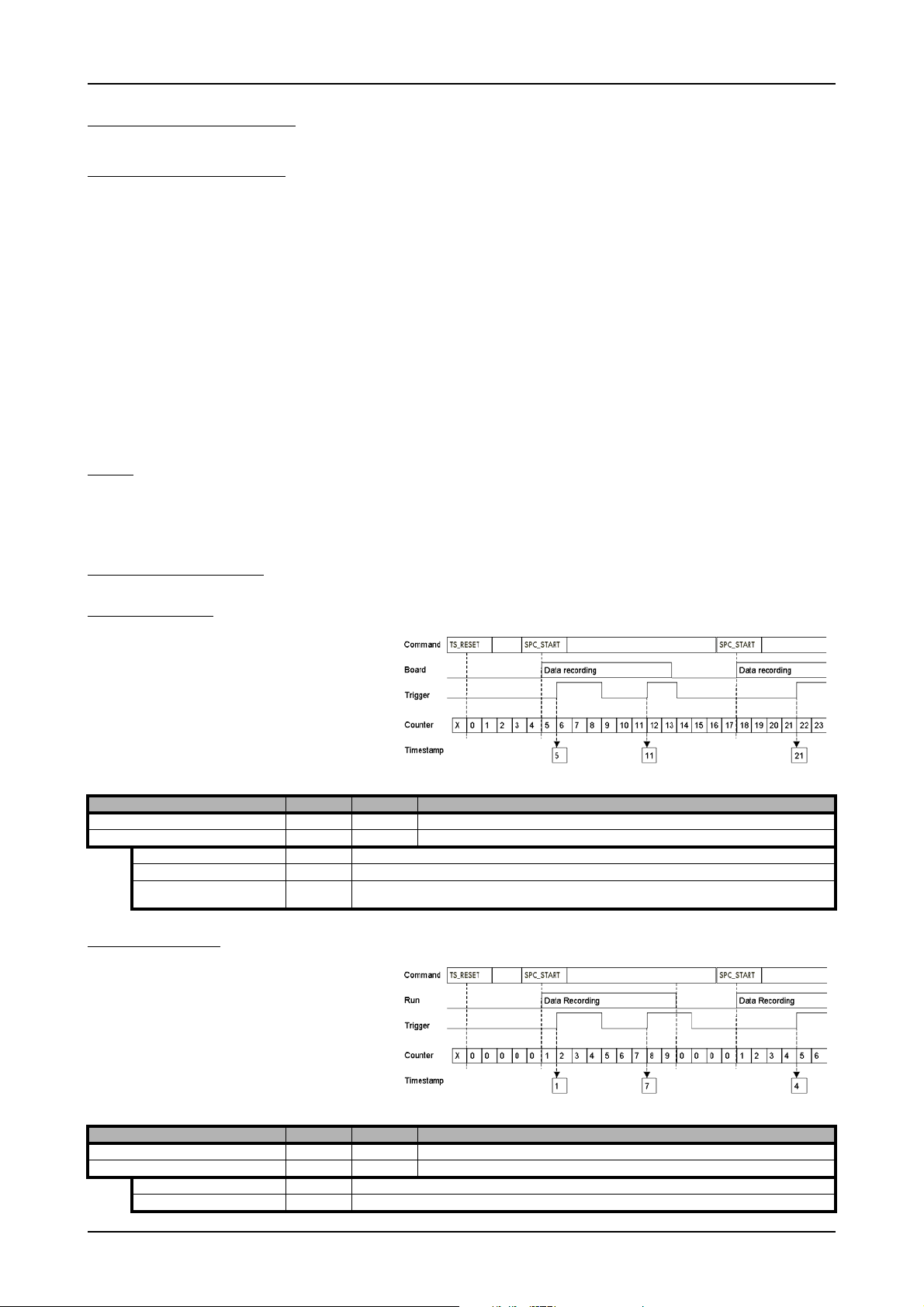
Option Timestamp General information
Option Timestamp
General information
The timestamp function is used to record trigger events relative to the beginning of the measurement, relative to a fixed time-zero point or
synchronized to an external radio clock. This is done by a wide resetable counter that is incremented with every sample rate. With every
detected trigger event the actual counter value is stored in a seperate timestamp memory.
This function is designed as an enhancement to the Multiple Recording and the Gated Sampling mode but can also be used without these
options. If Gated Sampling mode is used, then both the start and end of a recorded segment are timestamped.
The timestamp memory is designed as a FIFO buffer so that it can be read out even while the Spectrum board is recording data continuously
to the PC in the FIFO mode. This extra memory is 64 K Timestamps in size.
Each recorded timestamp consists of the number of samples that has been counted since the last
counter reset has been done. The actual time from the point since the last reset has been done so
t
--------------------------------------------------=
Sample rate
Timestamp
can easily be calculated by the formular besides.
If you want to know the time between two timestamps, you can simply calculate this by the formular besides.
Timestamp
-----------------------------------------------------------------------------------------------------------------------------
∆
=
t
n 1+
Sample rate
Timestamp
–
n
Limits
The timestamp counter is running with the sampling clock on the base card. Some card types (like 2030 and 3025) use an interlace mode
to double the sampling speed. In this case the timestamp counter is only running with the non-interlaced sampling rate. Therefore the maximum
counting frequency of the timestamp option is limited to 125 MS/s.
Timestamp modes
Standard mode
In standard mode the timestamp counter is set to zero
once by writing the TS_RESET commando to the command register. After that command the counter counts
continuously.
The timestamps of all recorded trigger events are referenced to this common zero time. With this mode you
can calculate the exact time difference between different recordings.
The following table shows the valid values that can be
written to the timestamp command register.
Register Value Direction Description
SPC_TIMESTAMP_CMD 47000 w Writes a command to the timestamp command register.
SPC_TIMESTAMP_CMD 47000 r Reads out the actual timestamp mode.
TS_RESET 0 Resets the counter of the timestamp module to zero.
TS_MODE_DISABLE 10 Disables the timestamp module. No timestamps are recorded.
TS_MODE_STANDARD 12 Must be written to enable the Standard timestamp mode. The counter must be manually reset by writing the command
TS_RESET to the command register. The timestamps values will be relative to this reset time.
StartReset mode
In StartReset mode the timestamp counter is set to zero
on every start of the board. After starting the board the
counter counts continuously.
The timestamps of one recording are referenced to the
start of the recording. This mode is very useful for Multiple Recording and Gated Sampling (see according
chapters for detailed information on these two optional
modes).
The following table shows the valid values that can be
written to the timestamp command register.
Register Value Direction Description
SPC_TIMESTAMP_CMD 47000 w Writes a command to the timestamp command register.
SPC_TIMESTAMP_CMD 47000 r Reads out the actual timestamp mode.
TS_RESET 0 Resets the counter of the timestamp module to zero.
TS_MODE_DISABLE 10 Disables the timestamp module. No timestamps are recorded.
(c) Spectrum GmbH 83
Page 84

Timestamp Status Option Timestamp
TS_MODE_STARTRESET 11 Must be written to enable the StartReset timestamp mode. The counter is reset on each start of the board. The times-
tamps values are relative to the board start.
RefClock mode (optional)
The counter is split in a HIGH and a LOW part and an additional seconds signal, that affects both parts of the counter (TTL pulse with f = 1
Hz) must be fed in externally.
The HIGH part counts the seconds that have elapsed since the last counter reset with the reset command TS_RESET. The LOW part is reset to
zero on every seconds signal and is clocked with the actual sample rate. The edge of the external secondssignal must be set seperately as
described below.
This mode allows the recording of an absolute time of a trigger event. This even allows the synchronization of data that has been recorded
with different boards.
Register Value Direction Description
SPC_TIMESTAMP_CMD 47000 w Writes a command to the timestamp command register.
SPC_TIMESTAMP_CMD 47000 r Reads out the actual timestamp mode.
TS_RESET 0 Resets the whole counter of the timestamp module to zero. Waits for synchronization to an external seconds signal.
TS_MODE_DISABLE 10 Disables the timestamp module. No timestamps are recorded.
TS_MODE_REFCLOCK 13 Must be written to enable the RefClock timestamp mode. The counter must be manually reset by writing the command
The edge of the external TTL seconds signal can be programmed by the following register either to detect the rising or falling edge.
Register Value Direction Description
SPC_TIMESTAMP_RESETMODE 47050 r/w Defines the active edge of the external fed in seconds signal to reset the lower part of the counter. The
TS_RESET_POS 10 The lower part of the counter will be reset on every rising edge of the external reset signal (seconds signal).
TS_RESET_NEG 20 The lower part of the counter will be reset on every falling edge of the external reset signal (seconds signal).
This may last up to 1 second. The lower part of the counter can be reset with the external fed in second signal. The
edge of the reset signal can be programmed with the SPC_TIMESTAMP_RESETMODE register as shown in the table
below.
TS_RESET to the command register. The counter is splitted into two parts. The upper part counts the seconds of an
external reference clock. The lower part is reset on each second signal and counts the samples.
values written here do not affect the timestamp command TS_RESET.
To get recordings in relation to each other it is importent to know the absolute start time. This time can be easily read out by the following
register. The time is given back in seconds since midnight (00:00:00), January 1, 1970, which is the standard ’time_t’ in C/C++.
Register Value Direction Description
SPC_TIMESTAMP_STARTTIME 47030 r Reads out the start time of the RefClock mode. Return value is the number of seconds since midnight
(00:00:00), January 1, 1970, which is the standard ’time_t’ in C/C++.
Timestamp Status
The timestamp module has its own status register for the timestamp FIFO. You can easily read out the FIFO status with the help of the timestamp
status register shown in the table below.
Register Value Direction Description
SPC_TIMESTAMP_STATUS 47010 r Reads the status of the timestamp FIFO.
TS_FIFO_EMPTY 0 The timestamp FIFO is still empty.
TS_FIFO_LESSHALF 1 There are values in the timestamp FIFO but less than half of the FIFO is filled.
TS_FIFO_MOREHALF 2 More than half of the FIFO is filled with timestamps.
TS_FIFO_OVERFLOW 3 The timestamp FIFO is full and possibly data has been lost.
Reading out timestamp data
Functions for accessing the data
There are two possibilities to access the timestamps that have been stored in the timestamp FIFO.
Reading out a single timestamp
You can read out one 32 bit value from the timestamp FIFO by using the register shown in the table below.
Register Value Direction Description
SPC_TIMESTAMP_FIFO 47040 r Get one 32 bit value from the timestamp FIFO. If the FIFO is empty a zero will be returned.
Because accessing the timestamp with this function will be done with single accesses, getting the value(s) this
way is much slower than using the SpcGetData function as described below.
84 MC.31xx Manual
Page 85

Option Timestamp Reading out timestamp data
Using this function will not give you back a whole timestamp, as the timestamp values are wider than 32 bit.
Please also refer to the section on the timestamp data format below.
Reading out all the timestamps with SpcGetData
When using the function SpcGetData the data stored in the timestamp FIFO will be read out in one block by the driver. The usage of the
function SpcGetData is described in the relating section earlier in this manual. The following list does only show the different parameters in
a very short way:
SpcGetData (nr, ch, start, len, data)
• nr: Number of the board (Windows). Linux users please refer to the Driver section for differences using linux.
• ch: Channel to be read out. Must be set to CH_TIMESTAMP (9999) to access timestamp FIFO.
• start: [Windows only:] Differing from the standard use, this parameter gives back the number of actually read timestamps and therefore
needs to be a pointer. Please refer to the example at the end of this chapter. Under linux please use the SPC_TIMESTAMP_COUNT register instead and program the „start“ parameter to zero.
• len: Number of timestamps that fit in the data buffer and so defines the number of timestamps to be read out.
• data: Huge buffer for the read out timestamps, that must have at least enough space for 8*len bytes.
It might be that you try to read out more timestamps than there actually are in the timestamp FIFO bacause you don’t know how many trigger
events have been detected. Please make use of the value given back by the parameter start to get to know what parts of your buffer contain
valid timestamps.
Register Value Direction Description
SPC_TIMESTAMP_COUNT 47020 r Return the number of timestamps that have been read be the prior SpcGetData call. Needs only to be
used under Linux.
Data format
Each timestamp is 56 bit long and internally mapped to 64 bit (8 bytes). The counter value contains the number of clocks that have been
recorded with the currently used sample rate since the last counter-reset has been done. The matching time can easily be calculated as described in the general information section at the beginning of this chapter.
The values the counter is counting and that are stored in the timestamp FIFO represent the moments the trigger event occures internally. Compared to the real external trigger event, these values are delayed. The delay is depending on the actual sample rate, the number of activated
channels and the used trigger mode. This delay can be ignored, as it will be identically for all recordings with the same setup.
Timestamp Mode Recording Mode
Standard/StartReset Normal / Multiple Recording Trigger 0
Standard/StartReset Gated Sampling Gate Start 0
RefClock Normal / Multiple Recording Trigger 0
RefClock Gated Sampling Gate Start 0
1st 4 bytes 2nd 4 bytes 3rd 4 bytes 4th 4 bytes 5th 4 bytes 6th 4 bytes
LOW part
LOW part
Counter value
Counter value
Trigger 0
HIGH part
Gate Start 0
HIGH part
Trigger 0
Seconds
Gate Start 0
Seconds
Trigger 1
LOW part
Gate End 0
LOW part
Trigger 1
Counter value
Gate End 0
Counter value
Trigger 1
HIGH part
Gate End 0
HIGH part
Trigger 1
Seconds
Gate End 0
Seconds
Trigger 2
LOW part
Gate Start 1
LOW part
Trigger 2
Counter value
Gate Start 1
Counter value
Trigger 2
HIGH part
Gate Start 1
HIGH part
Trigger 2
Seconds
Gate Start 1
Seconds
(c) Spectrum GmbH 85
Page 86

Example programs Option Timestamp
Example programs
Standard acquisition mode
// ----- Allocate memory for the timestamp data buffer ----plTimeStamps = (ptr32) malloc (MAX_TIMESTAMPS * 8);
// ----- Reset the board and flush the FIFO ----SpcSetParam (hDrv, SPC_COMMAND, SPC_RESET);
// ----- Setup and start timestamp module ----SpcSetParam (hDrv, SPC_TIMESTAMP_CMD, TS_MODE_STANDARD); // Standard mode set
SpcSetParam (hDrv, SPC_TIMESTAMP_CMD, TS_RESET); // Counter is set to Zero
// ----- Start the board 4 times to generate 4 timestamps ----for (i=0; i<4; i++)
{
SpcSetParam (hDrv, SPC_COMMAND, SPC_START); // Start recording
do
{
SpcGetParam (hDrv, SPC_STATUS, &lStatus); // Wait for Status Ready
}
while (lStatus != SPC_READY);
}
// ----- Read out and display the timestamps ----SpcGetData (hDrv, CH_TIMESTAMP, (int32) &lCount, MAX_TIMESTAMPS, (dataptr) plTimeStamps);
for (i=0; i<lCount; i++)
printf ("Timestamp: %d\tHIGH: %08lx\tLOW: %08lx\n", i, plTimeStamps[2*i+1], plTimeStamps[2*i]);
// ----- Free the allocated memory for the timestamp data buffer ----free (plTimeStamps);
}
Acquisition with Multiple Recording
// ----- Reset the board and flush the FIFO ----SpcSetParam (hDrv, SPC_COMMAND, SPC_RESET);
// ----- Simple setup for recording ----SpcSetParam (hDrv, SPC_CHENABLE, 1); // 1 channel for recording
SpcSetParam (hDrv, SPC_SAMPLERATE, 1000000); // Samplerate 1 MHz.
SpcSetParam (hDrv, SPC_TRIGGERMODE, TM_TTLPOS); // External positive Edge
SpcSetParam (hDrv, SPC_MULTI, 1); // Enable Multiple Recording
SpcSetParam (hDrv, SPC_MEMSIZE, 8192); // 8k Memsize
SpcSetParam (hDrv, SPC_POSTTRIGGER, 1024); // Each segment 1k = 8 segments
SpcSetParam (hDrv, SPC_MULTI, 1); // Enable Multiple Recording
// ----- Setup and start timestamp module ----SpcSetParam (hDrv, SPC_TIMESTAMP_CMD, TS_MODE_STANDARD); // Standard Timestamp mode set
SpcSetParam (hDrv, SPC_TIMESTAMP_CMD, TS_RESET); // Counter is set to Zero
// ----- Start the board ----SpcSetParam (hDrv, SPC_COMMAND, SPC_START); // Start recording
do
{
SpcGetParam (hDrv, SPC_STATUS, &lStatus); // Wait for Status Ready
}
while (lStatus != SPC_READY);
// ----- Read out the timestamps ----SpcGetData (hDrv, CH_TIMESTAMP, (int32) &lCount, 8, (dataptr) plTimeStamps);
// ----- display the timestamps (There should be 8 stamps, 1 for each segment) ----for (i=0; i<lCount; i++)
printf (“Segment: %d Counter: %08lx %08lx\n”, i, plTimeStamps[2*i+1], plTimeStamps[2*i]);
86 MC.31xx Manual
Page 87

Option Extra I/O Digital I/Os
Option Extra I/O
Digital I/Os
With this simple-to-use enhancement it is possible to control a wide range of external instruments or other equipment. Therefore you have
several digital I/Os and the 4 analog outputs available. All extra I/O lines are completely independent from the board’s function, data direction or sample rate and directly controlled by software (asynchronous I/Os).
The extra I/O option is useful if an external amplifier should be controlled, any kind of signal source must be programmed, an antenna must
be adjusted, a status information from external machine has to be obtained or different test signals have to be routed to the board.
It is not possible to use this option together with the star hub or timestamp option, because there is just space
for one piggyback module on the on-board expansion slot.
Channel direction
Option -XMF (external connector)
The additional inputs and outputs are mounted on an extra bracket.
The direction of the 24 available digital lines can be programmed for every group of eight lines. The table below shows the direction register
and the possible values. To combine the values so simply have to OR them bitwise.
Register Value Direction Description
SPC_XIO_DIRECTION 47100 r/w Defines bytewise the direction of the digital I/O lines. The values can be combined by a bitwise OR.
XD_CH0_INPUT 0 Sets the direction of channel 0 (bit D7…D0) to input.
XD_CH1_INPUT 0 Sets the direction of channel 1 (bit D15…D8) to input.
XD_CH2_INPUT 0 Sets the direction of channel 2 (bit D23…D16) to input.
XD_CH0_OUTPUT 1 Sets the direction of channel 0 (bit D7…D0) to output.
XD_CH1_OUTPUT 2 Sets the direction of channel 1 (bit D15…D8) to output.
XD_CH2_OUTPUT 4 Sets the direction of channel 2 (bit D23…D16) to output.
Transfer Data
The outputs can be written or read by a single 32 bit register. If the register is read, the actual pin data will be taken. Therefore reading the
data of outputs gives back the generated pattern. The single bits of the digital I/O lines correspond with the bitnumber of the 32 bit register.
Values written to the most significant byte will be ignored.
Register Value Direction Description
SPC_XIO_DIGITALIO 47110 r Reads the data directly from the pins of all digital I/O lines either if they are declared as inputs or
SPC_XIO_DIGITALIO 47110 w Writes the data to all digital I/O lines that are declared as outputs. Bytes that are declared as inputs
outputs.
will ignore the written data.
Analog Outputs
In addition to the digital I/Os there are four analog outputs available. These outputs are directly programmed with the voltage values in mV.
As the analog outputs are driven by a 12 bit DAC, the output voltage can be set in a stepsize of 5 mV. The table below shows the registers,
you must write the desired levels too. If you read these outputs, the actual output level is given back from an internal software register.
Register Value Direction Description Offset range
SPC_XIO_ANALOGOUT0 47120 r/w Defines the output value for the analog output A0. ± 10000 mV in steps of 5 mV
SPC_XIO_ANALOGOUT1 47121 r/w Defines the output value for the analog output A1. ± 10000 mV in steps of 5 mV
SPC_XIO_ANALOGOUT2 47122 r/w Defines the output value for the analog output A2. ± 10000 mV in steps of 5 mV
SPC_XIO_ANALOGOUT3 47123 r/w Defines the output value for the analog output A3. ± 10000 mV in steps of 5 mV
After programming the levels of all analog outputs by the registers above, you have to update the analog outputs. This is done by the register
shown in the table below. To update all of the outputs all you need to do is write a “1“ to the dedicated register.
Register Value Direction Description
SPC_XIO_WRITEDACS 47130 w All the analog outputs are simultaniously updated by the programmed levels if a “1“ is written.
(c) Spectrum GmbH 87
Page 88

Programming example Option Extra I/O
Programming example
The following example shows how to use either the digital I/O#s and the analog outputs.
// ----- output 8 bit on D7 to D0 and read 8 bit on D15 to D8 ----SpcSetParam (hDrv, SPC_XIO_DIRECTION, XD_CH0_OUTPUT | XD_CH1_INPUT); // set directions of digital I/O transfer
SpcSetParam (hDrv, SPC_XIO_DIGITALIO, 0x00005A); // write data to D7-D0
SpcGetParam (hDrv, SPC_XIO_DIGITALIO, &lData); // read data and write values to lData
// ----- write some values to the analog channels. ----SpcSetParam (hDrv, SPC_XIO_ANALOGOUT0, -2000); // -2000 mV = -2.0 V
SpcSetParam (hDrv, SPC_XIO_ANALOGOUT1, 0); // 0 mV = 0.0 V
SpcSetParam (hDrv, SPC_XIO_ANALOGOUT2, +3500); // 3500 mV = 3.5 V
SpcSetParam (hDrv, SPC_XIO_ANALOGOUT3, +10000); // 10000 mV = 10.0 V
SpcSetParam (hDrv, SPC_XIO_WRITEDACS, 1); // Write data simultaneously to DAC
88 MC.31xx Manual
Page 89

Option Digital inputs
Option Digital inputs
This option allows the user to acquire additional digital channels synchronous and phasestable along with the analog data.
Therefore the analog data is filled up with the digital bits up to 16 Bit data width. This leads to a possibility of acquiring 4 additional digital
bits per channel with 12 bit resolution boards.
Sample format
The following table shows the sample format of the standard mode with the digital inputs disabled and the sample format with activated
digital inputs.
Bit Standard Mode Digital Inputs enabled
D15 ADx Bit 11 DIGx Bit 3
D14 ADx Bit 11 DIGx Bit 2
D13 ADx Bit 11 DIGx Bit 1
D12 ADx Bit 11 DIGx Bit 0
D11 ADx Bit 11(MSB) ADx Bit 11(MSB)
D10 ADx Bit 10 ADx Bit 10
D9 ADx Bit 9 ADx Bit 9
D8 ADx Bit 8 ADx Bit 8
D7 ADx Bit 7 ADx Bit 7
D6 ADx Bit 6 ADx Bit 6
D5 ADx Bit 5 ADx Bit 5
D4 ADx Bit 4 ADx Bit 4
D3 ADx Bit 3 ADx Bit 3
D2 ADx Bit 2 ADx Bit 2
D1 ADx Bit 1 ADx Bit 1
D0 ADx Bit 0 (LSB) ADx Bit 0 (LSB)
To enable the recording of the digital inputs you simply have to set the according register shown in the table below.
Register Value Direction Description
SPC_READDIGITAL 110100 read/write Enables the recording of the digital inputs. This is only possible if the option “digital inputs“ is
installed on the board.
Due to technical issues there is a board dependant fixed delay between the analog and digital samples. The
delay for your type of board can be found in the technical data section.
(c) Spectrum GmbH 89
Page 90

The different synchronization options Synchronization (Option)
Synchronization (Option)
This option allows the connection of multiple boards to generate a multi-channel system. It is possible to synchronize multiple Spectrum boards
of the same type as well as different board types. Therefore the synchronized boards must be linked concerning the board’s system clock and
the trigger signals.
If no synchronization is desired for a certain board you can exclude it by setting the register shown in the following table. This must be done
seperately for every board that should not work synchronized.
Register Value Direction Description
SPC_COMMAND 0 r/w Command register of the board
SPC_NOSYNC 120 Disables the synchronization globally.
The different synchronization options
Synchronization with option cascading
With the option cascading up to four Spectrum boards can be synchronized. All boards are connected with one synchronization cable on
their sync-connectors (for details please refer to the chapter about installing the hardware).
As the synchronization lines are organized as a bus topology, there is a need for termination at both ends of the
bus. This is done in factory for the both end-boards. The maximum possible two middle-boards have no termination
on board.
When synchronizing multiple boards, one is set to be the clock master for all the connected boards. All the other
boards are working as clock slaves. It’s also possible to temporarily disable boards from the synchronization.
The same board or another one of the connected boards can be defined as a trigger master for all boards. All
trigger modes of the trigger master board can be used. It is also possible to synchronize the connected boards only
for the samplerate and not for trigger. This can be useful if one generator board is continuously generating a testpattern, while the connected acquisition board is triggering for test results or error conditions of the device under test.
For the fact that the termination is set in factory the order of the syncronized boards cannot be changed by
the user. Please refer to the boards type plate for details on the board’s termination. End boards are marked
with the option „cs-end“ while middle boards are marked with the option „cs-mid“
When the boards are synchronized by the option cascading
there will be a delay of about 500 ps between two adjacent
boards.
The figure on the right shows the clocks of three cascaded
boards with two channels each, where one end-board is defined as a clock master. Slave 1 is therefore a middle-board
and Slave 2 is the other end-board. The resulting delay between data of the two end-boards is therefore about 1 ns.
Please keep in mind that the delay between the channels of
two boards is depending on which board is actually set up as
the clock master and what boards are directly adjacent to the
master.
Synchronization with option starhub
With the option starhub up to 16 Spectrum boards can be synchronized. All boards are connected with a seperate synchronization cable
from their sync-connectors to the starhub module, which is a piggy-back module on one Spectrum board (for details please refer to the chapter
about installing the hardware).
When synchronizing multiple boards, one is set to be the clock master for all the connected boards. All the other boards are working as clock
slaves. It’s also possible to temporarily disable the synchronization of one board. This board then runs individually while the other boards
still are synchronized.
The same board or another one of the connected boards can be defined as a trigger master for all boards. All trigger modes of the board
defined as the trigger master can be used. It is also possible to synchronize the connected boards only for the samplerate and not for trigger.
This can be useful, if one generator board is continuously generating a testpattern, while the connected acquisition board is triggering for
test results or error conditions of the device under test.
Additionally you can even define more than one board as a trigger master. The trigger events of all boards are combined by a
logical OR, so that the first board that detects a trigger will start the boards. This OR connection is available starting with starhub
hardware version V4.
90 MC.31xx Manual
Page 91

Synchronization (Option) The setup order for the different synchronization options
When the boards are synchronized by the option starhub there
will be no delay between the connected boards. This is
achieved as all boards, including the one the starhub module
is mounted on, are connected to the starhub with cables of the
same length.
The figure on the right shows the clock of three boards with two
channels each that are synchronized by starhub.
The setup order for the different synchronization options
If you setup the boards for the use with synchronization it is important to keep the order within the software
commands as mentioned below to get the boards working correctly.
Depending on if you use the board either in standard or in FIFO mode there are slightly different orders in the setup for the synchronization
option. The following steps are showing the setups either for standard or FIFO mode.
Setup Order for use with standard (non FIFO) mode and equally clocked boards
(1) Set up the board parameters
Set all parameters like for example sample rate, memsize and trigger modes for all the synchronized boards, except the dedicated registers
for the synchronization itself that are shown in the tables below.
All boards must be set to the same settings for the entire clocking registers (see the according chapter for sample rate generation), for the
trigger mode and memory and should be set to the same postcounter size to get the same pretrigger sizes as well.
If you use acquisition boards with different pretrigger sizes, please keep in mind that after starting the board
the pretrigger memory of all boards will be recorded first, before the boards trigger detection is armed. Take
care to prevent boards with a long pretrigger setup time from hangup by adequately checking the board’s
status. Long setup times are needed if either you use a huge pretrigger size and/or a slow sample rate.
If you don’t care it might happen that boards with a small pretrigger are armed first and detect a triggerevent, while one or more boards with
a huge pretrigger are still not armed. This might lead to an endless waiting-state on these boards, which should be avoided.
Example of board setup for three boards
// --------- Set the Handles to fit for Windows driver --------hDrv[0] = 0;
hDrv[1] = 1;
hDrv[2] = 2;
// (1) ----- Setup all boards, shortened here !!!----for (i = 0; i < 3; i++)
{
SpcSetParam (hDrv[i], SPC_MEMSIZE, 1024); // memory in samples per channel
SpcSetParam (hDrv[i], SPC_POSTTRIGGER, 512); // posttrigger in samples
// ...
SpcSetParam (hDrv[i], SPC_SAMPLERATE, 10000000); // set sample rate to all boards
SpcSetParam (hDrv[i], SPC_TRIGGERMODE, TM_SOFTWARE); // set trigger mode to all boards
}
(2) Let the master calculate it’s clocking
To obtain proper clock initailization when doing the first start it is necessary to let the clock master do all clock related calculations prior to
setting all the synchronization configuration for the slave boards.
Example of board #0 set as clock master and forced to do the appropriate clock calculation
SpcSetParam (hDrv[0], SPC_COMMAND, SPC_SYNCCALCMASTER); // Calculate clock settings on master
(3) Write Data to on-board memory (output boards only)
If one or more of the synchronized boards are used for generating data (arbitrary waveform generator boards or digital I/O boards with
one or more channels set to output direction) you have to transfer the data to the board’s on-board memory before starting the synchronization.
Please refer to the related chapter for the standard mode in this manual. If none of your synchronized boards is used for generation purposes
you can ignore this step.
(c) Spectrum GmbH 91
Page 92

The setup order for the different synchronization options Synchronization (Option)
Example for data writing
SpcSetData (hDrv[0], 0, 0, 1024, pData[0]);
SpcSetData (hDrv[1], 0, 0, 1024, pData[1]);
SpcSetData (hDrv[2], 0, 0, 1024, pData[2]);
(4) Define the board(s) for trigger master
At least one board must be set as the trigger master to get synchronization running. Every one of the synchronized boards can be programmed
for beeing the trigger master device.
Register Value Direction Description
SPC_COMMAND 0 r/w Command register of the board
SPC_SYNCTRIGGERMASTER 101 Defines the according board as the triggermaster.
Example of board #2 set as trigger master
SpcSetParam (hDrv[2], SPC_COMMAND, SPC_SYNCTRIGGERMASTER); // Set board 2 to trigger master
(4a) Define synchronization OR trigger
If you use synchronization with the starhub option you can even set up more than one board as the trigger master. The boards will be combined by a logical OR and therefore the boards will be started if any of the trigger masters has detected a trigger event.
The synchronization OR-trigger is not available when using the cascading option. It is also not available with
starhub option prior to hardware version V4. See the initialization section of this manual to find out how to
determint the hardware version of the starhub.
If you set up the boards for the synchronization OR trigger all boards that are set as trigger master must be programmed to the same triggermode. If the boards are using different trigger modes this will result in a time shift between the boards. It is of course possible to set different
edges or different trigger levels on the channels.
It is only possible to use the synchronization OR trigger if the board carrying the starhub piggy-back module
is one of the boards that is programmed as a trigger master.
To find out what board is carrying the starhub piggy-back module you make use of the board’s feature registers as described in the
chapter about initialising the board.
Example of setting up three boards to be trigger master
SpcSetParam (hDrv[0], SPC_COMMAND, SPC_SYNCTRIGGERMASTER); // Set board 0 to trigger master
SpcSetParam (hDrv[1], SPC_COMMAND, SPC_SYNCTRIGGERMASTER); // Set board 1 to trigger master
SpcSetParam (hDrv[2], SPC_COMMAND, SPC_SYNCTRIGGERMASTER); // Set board 2 to trigger master
(5) Define the remaining boards as trigger slaves
As you can set more than one board as the trigger master (starhub option only) you have to tell the driver additionally which of the boards
are working as trigger slaves.
Register Value Direction Description
SPC_COMMAND 0 r/w Command register of the board
SPC_SYNCTRIGGERSLAVE 111 Defines the according board as the trigger slave.
Each of the synchronized boards must be set up either as a trigger master or as a trigger slave to get the
synchronization option working correctly. Therefore it does not matter if you use the cascading or starhub
option.
It is assumed that only one of the three boards (board 2 in this case) is set up as trigger master, as described in (3)
SpcSetParam (hDrv[0], SPC_COMMAND, SPC_SYNCTRIGGERSLAVE); // Setting all the other boards to
SpcSetParam (hDrv[1], SPC_COMMAND, SPC_SYNCTRIGGERSLAVE); // trigger slave is a must !
It sometimes might be necessary to exclude one or more boards from the synchronization trigger. An example for this solution is that one or
more output boards are used for continuously generating test patterns, while one or more acqusition boards are triggering for test results or
error conditions. Therefore it is possible to exclude a board from the triggerbus so that only a synchronization for clock is done and the according boards are just using the trigger events they have detected on their own.
Register Value Direction Description
SPC_NOTRIGSYNC 200040 r/w If activated the dedicated board will use its own trigger modes instead of the synchronization trigger.
92 MC.31xx Manual
Page 93

Synchronization (Option) The setup order for the different synchronization options
Even if a board is not using the synchronization trigger, it must have been set as a triggerslave before even
if you exclude the board with the SPC_NOTRIGSYNC register.
After you have excluded one or more of the installed boards from the synchronization trigger it is possible to change the triggermodes
of these boards. So only all the boards that should work synchronously must be set up for the same trigger modes to get the synchronization mode working correctly.
(6) Define the board for clock master
Using the synchronization option requires one board to be set up as the clock master for all the synchronized board. It is not allowed to set
more than one board to clock master.
Register Value Direction Description
SPC_COMMAND 0 r/w Command register of the board
SPC_SYNCMASTER 100 Defines the according board as the clock master for operating in standard (non FIFO) mode only.
Example: board number 0 is clock master
SpcSetParam (hDrv[0], SPC_COMMAND, SPC_SYNCMASTER); // Set board 0 to clock master
(7) Define the remaining boards as clock slaves
It is necessary to set all the remaining boards to clock slaves to obtain correct internal driver settings.
Register Value Direction Description
SPC_COMMAND 0 r/w Command register of the board
SPC_SYNCSLAVE 110 Defines the according board as a clock slave for operating in standard (non FIFO) mode only.
Settings the remining boards to clock slaves. Board number 0 is clock master in the example
SpcSetParam (hDrv[1], SPC_COMMAND, SPC_SYNCSLAVE); // Setting all the other boards to
SpcSetParam (hDrv[2], SPC_COMMAND, SPC_SYNCSLAVE); // clock slave is a must !
(8) Arm the boards for synchronization
Before you can start every single one of the synchronized boards on their own you have to arm all the synchronized boards before for the
use with synchronization. The synchronization has to be started on the clock master board.
Register Value Direction Description
SPC_COMMAND 0 r/w Command register of the board
SPC_SYNCSTART 130 Arms all boards for the use with synchronization.
Example of starting the synchronization. Board number 0 is clock master.
SpcSetParam (hDrv[0], SPC_COMMAND, SPC_SYNCSTART);
(9) Start all of the trigger slave boards
After having armed the synchronized boards, you must start all of the boards that are defined as trigger slaves first.
Register Value Direction Description
SPC_COMMAND 0 r/w Command register of the board
SPC_START 10 Starts the board with the current register settings.
SPC_STARTANDWAIT 11 Starts the board with the current register settings in the interrupt driven mode.
For details on how to start the board in the different modes in standard mode (non FIFO) please refer to the according chapter earlier in this
manual.
If using the interrupt driven mode SPC_STARTANDWAIT it is necessary to start each board in it’s own software
thread. This is necessary because the function does not return until the board has stopped again. If not using
different threads this will result in a program deadlock.
Example of starting trigger slave boards. Board number 2 is trigger master.
SpcSetParam (hDrv[0], SPC_COMMAND, SPC_START);
SpcSetParam (hDrv[1], SPC_COMMAND, SPC_START);
(c) Spectrum GmbH 93
Page 94

Setup synchronization for use with FIFO mode and equally clokked boards Synchronization (Option)
(10) Start all of the trigger master boards
After having armed the synchronized boards, you must start all of the boards, that are defined as trigger masters.
Register Value Direction Description
SPC_COMMAND 0 r/w Command register of the board
SPC_START 10 Starts the board with the current register settings.
SPC_STARTANDWAIT 11 Starts the board with the current register settings in the interrupt driven mode.
For details on how to start the board in the different modes in standard mode (non FIFO) please refer to the according chapter earlier in this
manual.
If you use the synchronization OR with the starhub option it is important to start the board carrying the
starhub piggy-back module as last. Otherwise the trigger masters that are started first might detect trigger
events while other trigger masters haven’t even been started. Be sure that the pretrigger area of all other
trigger masters is filled at the moment when the pretrigger area of the star-hub board has been filled.
To find out what board is carrying the starhub piggy-back module you make use of the board’s feature registers as described in the chapter
about programming the board.
Example of starting the trigger master board
SpcSetParam (hDrv[2], SPC_COMMAND, SPC_START);
(11) Wait for the end of the measurement
After having started the last board, you will have to wait until the measurement is done. Depending if you use the board in standard (non
FIFO) mode interrupt driven or not, you can poll for the board’s status. Please refer to the relating chapter in this manual. It is necessary to
wait until each board returns the status SPC_READY before proceeding.
Example for polling for three synchronzed boards
for (i = 0; i < 3; i++) // For all synchronized boards
do // The status is read out
{
SpcGetParam (hDrv[i], SPC_STATUS, &lStatus); // by polling for SPC_READY
}
while (lStatus != SPC_READY);
}
printf (“All boards have stopped“);
(12) Read data from the on-board memory (acquisition boards only)
If one or more of the synchronized boards are used for recording data (transient recorder boards or digital I/O boards with one or more
channels set to input direction) you have to read out the data from the board’s on-board memory now. Please refer to the related chapter for
the standard (non FIFO) mode in this manual. If none of your synchronized boards is used for recording purposes you can ignore this step.
Example for data reading
SpcGetData (hDrv[0], 0, 0, 1024, pData[0]);
SpcGetData (hDrv[1], 0, 0, 1024, pData[1]);
SpcGetData (hDrv[2], 0, 0, 1024, pData[2]);
(13) Restarting the board for another synchronized run
If you want to restart the synchronized boards with the same settings as before it is sufficient to repeat only the steps starting with (8). This
assumes that on generation boards the output data is not changed as well.
If you want to change the output data of generation boards you’ll have to restart the setup procedure starting with step (2).
If you even want to change any of the boards parameters you’ll have to restart the setup procedure from the first step on.
Setup synchronization for use with FIFO mode and equally clokked boards
Most of the steps are similar to the setup routine for standard synchronization mentioned before. In this passage only the differences between
the two modes are shown. Please have a look at the passage before to see the complete setup procedure. The following steps differ from
standard mode to FIFO mode. All steps that are not mentioned here are similar as described before.
(2) Allocate the FIFO software buffers
If you use the board in FIFO mode additional memory in the PC RAM is needed for software FIFO buffers. For details please refer to the
according chapter for the FIFO mode.
94 MC.31xx Manual
Page 95

Synchronization (Option) Setup synchronization for use with FIFO mode and equally clokked boards
Example of FIFO buffer allocation:
for (i = 0; i < FIFO_BUFFERS; i++)
for (b = 0; b < 3; b++)
{
pnData[b][i] = (ptr16) GlobalAlloc (GMEM_FIXED, FIFO_BUFLEN); // allocate memory
SpcSetParam (b, SPC_FIFO_BUFADR0 + i, (int32) pnData[b][i]); // send the adress to the driver
}
(2a) Write first data for output boards
When using the synchronization FIFO mode with output boards this is the right position to fill the first software buffers with data. As you can
read in the FIFO chapter, output boards need some data to be written to the software FIFO buffers before starting he board.
Example of calulcating and writing output data to software FIFO buffers:
// ----- data calculation routine ----int g_nPos =0; // some global variables
void vCalcOutputData (ptr16 pnData, int32 lBufsize) // function to calculate the
{ // output data. In this case
int i; // a sine function is used.
for (i = 0; i < (lBufsize/2); i++)
pnData[b][i] = (int16) (8191.0 * sin (2 * PI / 500000 * (g_nPos+i)));
g_nPos += lBufsize/2;
}
// ----- main task ----int main(int argc, char **argv)
{
...
for (i =0; i < MAX_BUF; i++) // fill the first buffers with data
for (b = 0; b < 3; b++) // for all installed boards
vCalcOutputData (pnData[b][i], BUFSIZE);
...
}
(6) Define the board for clock master
Using the synchronization option requires one board to be set up as the clock master for all the synchronized board. It is not allowed to set
more than one board to clock master.
Register Value Direction Description
SPC_COMMAND 0 r/w Command register of the board
SPC_SYNCMASTERFIFO 102 Defines the according board as the clock master for operating in FIFO mode only.
Example: board number 0 is clock master
SpcSetParam (hDrv[0], SPC_COMMAND, SPC_SYNCMASTERFIFO); // Set board 0 to clock master
(7) Define the remaining boards as clock slaves
It is necessary to set all the remaining boards to clock slaves to obtain correct internal driver settings.
Register Value Direction Description
SPC_COMMAND 0 r/w Command register of the board
SPC_SYNCSLAVEFIFO 102 Defines the according board as a clock slave for operating in FIFO mode only.
Settings the remaining boards to clock slaves. Board number 0 is clock master in the example
SpcSetParam (hDrv[1], SPC_COMMAND, SPC_SYNCSLAVEFIFO); // Setting all the other boards to
SpcSetParam (hDrv[2], SPC_COMMAND, SPC_SYNCSLAVEFIFO); // clock slave is a must !
(9) Start all of the trigger slave boards
After having armed the synchronized boards, you must start all of the boards, that are defined as trigger slaves first. This is done with the
FIFOSTART command.
Register Value Direction Description
SPC_COMMAND 0 r/w Command register of the board
SPC_FIFOSTART 10 Starts the board with the current register settings in FIFO mode and waits for the first interrupt.
Remember that the FIFO mode is allways interrupt driven. As a result the FIFOSTART function will not return
until the first software buffer is transferred. For that reason it is absolutely necessary to start different threads
(c) Spectrum GmbH 95
Page 96

Setup synchronization for use with FIFO mode and equally clokked boards Synchronization (Option)
for each board that runs synchronuously in FIFO mode. If this is not done a deadlock will occur and the program will
not start properly.
(10) Start all of the trigger master boards
After having armed the synchronized boards, you must start all of the boards, that are defined as trigger masters.
Register Value Direction Description
SPC_COMMAND 0 r/w Command register of the board
SPC_FIFOSTART 10 Starts the board with the current register settings in FIFO mode and waits for the first interrupt.
This example shows how to set up three boards for synchronization in FIFO mode. Board 0 is clock master and board 2 is trigger master.
// (3) ----- trigger synchronization of trigger master board(s) ---- SpcSetParam (hDrv[2], SPC_COMMAND, SPC_SYNCTRIGGERMASTER); // board 2 set as trigger master
// (4) ----- trigger synchronization of trigger slave boards ---- SpcSetParam (hDrv[0], SPC_COMMAND, SPC_SYNCTRIGGERSLAVE); // as trigger slaves
SpcSetParam (hDrv[1], SPC_COMMAND, SPC_SYNCTRIGGERSLAVE); // as trigger slaves
// (5) ----- synchronization information for clock master board ---- SpcSetParam (hDrv[0], SPC_COMMAND, SPC_SYNCMASTERFIFO);
// (6) ----- synchronization information for clock slave boards ---- SpcSetParam (hDrv[1], SPC_COMMAND, SPC_SYNCSLAVEFIFO);
SpcSetParam (hDrv[2], SPC_COMMAND, SPC_SYNCSLAVEFIFO);
// (7) ----- start the synchronization ---- SpcSetParam (hDrv[0], SPC_COMMAND, SPC_SYNCSTART);
// (8) ----- start the FIFO tasks. Trigger slaves are started first ---- CreateThread (NULL, 0, &dwFIFOTask, (void*) hDrv[0], 0, &dwThreadId[b]);
CreateThread (NULL, 0, &dwFIFOTask, (void*) hDRV[1], 0, &dwThreadId[b]);
// (9) ----- start the trigger master FIFO task ---- CreateThread (NULL, 0, &dwFIFOTask, (void*) hDrv[2], 0, &dwThreadId[hDrv[2]]);
It is assumed, that the created threads start in the same order as they are called from within the program. As described before, starting of
the FIFO mode in synchronization has to be done in different threads to avoid a deadlock. A simple example for a FIFO thread can be found
below.
Example of FIFO task. It simply starts the boards and counts the buffers that have been transfered:
unsigned long __stdcall dwFIFOTask (void* phDrv)
{
int16 hDrv = (int16) phDrv;
int32 lCmd = SPC_FIFOSTART;
int16 nBufIdx = 0, nErr;
int32 lTotalBuf;
lTotalBuf = 0;
do
{
nErr = SpcSetParam (hDrv, SPC_COMMAND, lCmd); // wait for buffer
lCmd = SPC_FIFOWAIT; // here you can do
printf ("Board %d Buffer %d total buffers: %d\n", nIdx, nBufIdx, lTotalBuf);// e.g. calculations
// just a printf here
SpcSetParam (hDrv, SPC_COMMAND, SPC_FIFO_BUFREADY0 + nBufIdx); // release buffer
nBufIdx++;
lTotalBuf++;
if (nBufIdx == FIFO_BUFFERS)
nBufIdx = 0;
}
while (nErr == ERR_OK);
return 0;
}
Additions for synchronizing different boards
General information
Spectrum boards with different speed grades, different number of channels or even just different clock settings for the same types of boards
can be synchronized as well. To get the boards working together synchronously some extra setups have to be done, which are described in
the following passages.
96 MC.31xx Manual
Page 97

Synchronization (Option) Setup synchronization for use with FIFO mode and equally clokked boards
All clock rates of all synchronized boards are derived from the clock signal that is distributed via the sync bus. This clock is the sum samplerate
of one module of the clock master board. Based on this speed the clock rates of the slave boards can be set. As these clock rates are divided
from the sync clock, the board with the maximum sum sample rate should be set up as clock master.
Calculating the clock dividers
The sum sample rate can easily be calculated by the formula on the right.
The value for the sample rate of board N must contain the actual desired
SumSampleRateNSampleRate=
ActChPerModule
⋅
N
N
conversion rate for one channel of board N. Please refer to the dedicated
chapter in the board’s manual to get informed about the relation beween
the board model and the number of actually activated channels per module for the different channel setups.
As mentioned above the board with the highest sum sample rate must be
set up as the clock master. This maximum sum sample rate is used as the
overall sync speed, which is distributed via the sync bus. If you have calculated the sync speed you can calculate the clock dividers for the different boards with the formula on the right.
The maximum possible channels per module for all Spectrum boards are
given in the table below.
20xx x 30xx x 31xx x 40xx x 45xx x 60xx x 61xx x 70xx x 72xx x
0x 7005 1
1x 3010 1 3110 2 6110 2 7010 1 7210 1
3011 2 3111 4 6011 2 6111 2 7011 2 7211 1
3012 2 3112 4 6012 2
3013 2
3014 2
3015 1
3016 2
2x 2020 2 3020 1 3120 2 4020 1 4520 2 7020 1 7220 1
2021 2 3021 2 3121 4 4021 2 4521 2 6021 2 7021 2 7221 1
3022 2 3122 4 4022 2 6022 2
3023 2
3024 2
3025 1
3026 2
3027 1
3x 3130 2 4030 1 4530 2 6030 1
2031 2 3031 2 3131 4 4031 2 4531 2 6031 1
3132 4 4032 2
2033 2 3033 2 6033 2
6034 2
4x 4540 2
4541 2
(c) Spectrum GmbH 97
Page 98

Setup synchronization for use with FIFO mode and equally clokked boards Synchronization (Option)
Setting up the clock divider
The clock divider can easily be set by the following register. Please keep in mind that the divider must be set for every synchronized board
to have synchronization working correctly. For more details on the board’s clocking modes please refer to the according chapter in this manual.
Register Value Direction Description
SPC_CLOCKDIV 20040 r/w Extra clock divider for synchronizing different boards.
Available divider values
1 2 4 8 101620405080100200
400 500 800 1000 2000
The clock divider is also used by internal clock generation for all clock rates that are below 1 MS/s sum sample rate per module. If internal clock divider and extra clock divider are used together the resulting clock
divider is one value of the above listed. The driver searches for the best matching divider. Read out the register after all sample rate registers are set to receive the resulting extra clock divider. For correct setting of the clock
divider the sample rate and channel enable information must be set before the clock divider is programmed.
Although this setup is looking very complicated at first glance, it is not really difficult to set up different boards to work synchronously with the
same speed. To give you an idea on how to setup the boards the calculations are shown in the following two examples.
Each example contains of a simple setup of two synchronized boards. It is assumed that all of the available channels on the dedicated boards
have been activated.
Example calculation with synchronous speed where slave clock is divided
Board type 3122 3120
Channels available 8 x 12 bit A/D 2 x 12 bit A/D
Desired sample rate 10 MS/s 10 MS/s
Enabled channels per module 4 2
Sum sample rate 40 MS/s 20 MS/s
Therefore this board is set up
to be the clockmaster.
Sync speed 40 MS/s 40 MS/s
Clock divider 1 2
Divided sum clock 40 MS/s 20 MS/s
Enabled channels per module 4 2
Conversion speed 10 MS/s 10 MS/s
Example calculation with synchronous speed where master clock is divided
Board type 3025 3131
Channels available 2 x 12 bit A/D 4 x 12 bit A/D
Desired sample rate 20 MS/s 20 MS/s
Enabled channels per module 1 2
Sum sample rate 20 MS/s 40 MS/s
Therefore this board is set up
to be the clockmaster.
Sync speed 40 MS/s 40 MS/s
Clock divider 2 1
Divided sum clock 20 MS/s 40 MS/s
Enabled channels per module 1 2
Conversion speed 20 MS/s 20 MS/s
98 MC.31xx Manual
Page 99

Synchronization (Option) Setup synchronization for use with FIFO mode and equally clokked boards
Additions for equal boards with different sample rates
In addition to the possibility of synchronizing different types of boards to one synchronous sample rate it can be also useful in some cases to
synchronize boards of the same type, with one working at a divided speed.
In this case you simply set up the fastest board as the clock master and set it’s clock divider to one. Now you can easily generate divided
clock rates on the slave boards by setting their dividers to according values of the divider list.
Please keep in mind that only the dedicated divider values mentioned in the list above can be used to derive
the sample rates of the slave boards.
The following example calculation is explaining that case by using to acquisition boards. One of the boards is running with only a hundreth
of the other sample rate.
Example with equal boards but asynchronous speeds
Board type 3121 3121
Channels available 4 x 12 bit A/D 4 x 12 bit A/D
Desired sample rate 10 MS/s
Enabled channels per module 4 4
Sum sample rate 40 MS/s
This board is set up to be the
clockmaster now.
Sync speed 40 MS/s 40 MS/s
Clock divider (is set to) 1 100
Divided sum clock 40 MS/s 400 kS/s
Enabled channels per module 4 4
Conversion speed 10 MS/s 100 kS/s
Resulting delays using different boards or speeds
Delay in standard (non FIFO) modes
There is a fixed delay between the samples of the different boards depending on the type of board, the selected clock divider and the activated channels. This delay is fixed for data acquisition or generation with the same setup.
If you use generation boards in the single shot mode this delay will be compensated within the software driver automatically.
Delay in FIFO mode
When the FIFO mode is used a delay is occuring between the data of the different boards. This delay is depending on the type of board, the
selected clock divider and the activated channel. You can read out the actual resulting delay from every board with the following register.
Register Value Direction Description
SPC_STARTDELAY 295110 r Start delay in samples for FIFO synchronization only.
The resulting delay between the clock master board and the single clock
slave boards can be easily calculated with the formular mentioned on
the right.
ResultingDelay ClockMasterDelay ClockSlaveDelay
–=
N
(c) Spectrum GmbH 99
Page 100

Error Codes Appendix
Appendix
Error Codes
The following error codes could occur when a driver function has been called. Please check carefully the allowed setup for the register and
change the settings to run the program.
error name value (hex) value (dec.) error description
ERR_OK 0h 0 Execution OK, no error.
ERR_INIT 1h 1 The board number is not in the range of 0 to 15. When initialisation is executed: the board number is yet
ERR_NR 2h 2 The board is not initialised yet. Use the function SpcInitPCIBoards first. If using ISA boards the function SpcIn-
ERR_TYP 3h 3 Initialisation only: The type of board is unknown. This is a critical error. Please check whether the board is
ERR_FNCNOTSUPPORTED 4h 4 This function is not supported by the hardware version.
ERR_BRDREMAP 5h 5 The board index remap table in the registry is wrong. Either delete this table or check it craefully for double
ERR_KERNELVERSION 6h 6 The version of the kernel driver is not matching the version of the DLL. Please do a complete reinstallation of
ERR_HWDRVVERSION 7h 7 The hardware needs a newer driver version to run properly. Please install the driver that was delivered
ERR_LASTERR 10h 16 Old Error waiting to be read. Please read the full error information before proceeding. The driver is locked
ERR_ABORT 20h 32 Abort of wait function. This return value just tells that the function has been aborted from another thread.
ERR_BOARDLOCKED 30h 48 Access to the driver already locked by another program. Stop the other program before starting this one.
ERR_REG 100h 256 The register is not valid for this type of board.
ERR_VALUE 101h 257 The value for this register is not in a valid range. The allowed values and ranges are listed in the board spe-
ERR_FEATURE 102h 258 Feature (option) is not installed on this board. It’s not possible to access this feature if it’s not installed.
ERR_SEQUENCE 103h 259 Channel sequence is not allowed.
ERR_READABORT 104h 260 Data read is not allowed after aborting the data acquisition.
ERR_NOACCESS 105h 261 Access to this register denied. No access for user allowed.
ERR_POWERDOWN 106h 262 Not allowed if powerdown mode is activated.
ERR_TIMEOUT 107h 263 A timeout occured while waiting for an interrupt. Why this happens depends on the application. Please
ERR_CHANNEL 110h 272 The channel number may not be accessed on the board: Either it is not a valid channel number or the chan-
ERR_RUNNING 120h 288 The board is still running, this function is not available now or this register is not accessible now.
ERR_ADJUST 130h 304 Automatic adjustion has reported an error. Please check the boards inputs.
ERR_NOPCI 200h 512 No PCI BIOS is found on the system.
ERR_PCIVERSION 201h 513 The PCI bus has the wrong version. SPECTRUM PCI boards require PCI revision 2.1 or higher.
ERR_PCINOBOARDS 202h 514 No SPECTRUM PCI boards found. If you have a PCI board in your system please check whether it is cor-
ERR_PCICHECKSUM 203h 515 The checksum of the board information has failed. This could be a critical hardware failure. Restart the sys-
ERR_DMALOCKED 204h 516 DMA buffer not available now.
ERR_MEMALLOC 205h 517 Internal memory allocation failed. Please restart the system and be sure that there is enough free memory.
ERR_FIFOBUFOVERRUN 300h 768 Driver buffer overrun in FIFO mode. The hardware and the driver have been fast enough but the application
ERR_FIFOHWOVERRUN 301h 769 Hardware buffer overrun in FIFO mode. The hardware transfer and the driver has not been fast enough.
ERR_FIFOFINISHED 302h 770 FIFO transfer has been finished, programmed number of buffers has been transferred.
ERR_FIFOSETUP 309h 777 FIFO setup not possible, transfer rate to high (max 250 MB/s).
ERR_TIMESTAMP_SYNC 310h 784 Synchronisation to external timestamp reference clock failed. At initialisation is checked wether there is a
ERR_STARHUB 320h 800 The autorouting function of the star-hub initialisation has failed. Please check whether all cables are mounted
initialised, the old definition will be used.
itBoard must be called first.
correctly plug in the slot and whether you have the latest driver version.
values.
the hardware driver. This error normally only occurs if someone copies the dll manually to the system directory.
together with the board.
until the error information has been read.
Only one program can access the driver at the time.
cific documentation.
check whether the timeout value is programmed too small.
nel is not accessible due to the actual setup (e.g. Only channel 0 is accessible in interlace mode)
rectly plug into the slot connector and whether you have the latest driver version.
tem and check the connection of the board in the slot.
software didn’t manage to transfer the buffers in time.
Please check the system for bottlenecks and make sure that the driver thread has enough time to transfer
data.
clock edge present at the input.
correctly.
100 MC.31xx Manual
 Loading...