


−
−
−
SM8707 series
Clock Generator with Dual PLLs
OVERVIEW
The SM8707 series are dual-PLL clock generator ICs, using a 27MHz master clock, that generate independent
audio clock, video clock, and signal processor clock outputs needed in DVD player/recorder applications. Each
PLL loop filter and crystal oscillator circuit are built-in and require no external components, resulting in highprecision clocks. The lineup includes devices that support both 44.1/48kHz audio sampling frequencies (fs),
switchable using a control pin. The sampling frequency can be switched during operation without generating
any output spike noise.
FEATURES
■
Supply voltage: 3.0 to 3.6V
■
Low current consumption: 35mA typ.
(V
= 3.3V, all outputs with no load)
DD
27MHz master clock
■
(internal PLL reference clock)
Generated clocks (Refer to “Output Frequency Listing” on page 18 for details.)
■
SM8707D SM8707E SM8707F SM8707G SM8707H SM8707K SM8707L
Video system
output
Audio system
output
Signal processor
system output
1. 384fs (fs = 44.1kHz)/768fs (fs = 48kHz)
■
Low jitter output (1-sigma output load capacitance typical values)
27.0000MHz 27.0000MHz 27.0000MHz 27.0000MHz 27.0000MHz
512fs
1
768fs
1
384fs
16.9344MHz
33.8688MHz
512fs 768fs
33.8688MHz
16.9344MHz
33.8688MHz
■
PLL loop filter built-in
■
Crystal oscillator circuit built-in
Sampling frequency fs: 44.1/48kHz
■
16-pin VSOP package (Pb free)
■
512fs 768fs 768fs
18.4320MHz
24.5760MHz
33.8688MHz
36.8640MHz
33.8688MHz
16.9344MHz
33.8688MHz
36.8640MHz
27.0000MHz
24.5760MHz
33.8688MHz
SM8707D SM8707E SM8707F SM8707G SM8707H SM8707K SM8707L
Video system
output
Audio and Signal
processor
system output
20ps 20ps 20ps 20ps 20ps
70ps 55ps 40ps 40ps 70ps 60ps 60ps
APPLICATIONS
■
DVD players/recorders
■
DVD car navigation system
ORDERING INFORMATION
Device Package
SM8707DV
SM8707EV
SM8707FV
SM8707GV
SM8707HV
SM8707KV
SM8707LV
16-pin VSOP
PACKAGE DIMENSIONS
(Unit: mm)
Weight: 0.07g
4.4 0.2
6.4 0.2
0.275typ
5.1 0.2
0.65
+ 0.1
0.22
− 0.05
NIPPON PRECISION CIRCUITS INC.—1
1.15 0.1
0.10 0.05
0.10
M
0.12
0.5 0.2
0.15
+ 0.1
20ps
- 0.05
0 to 10
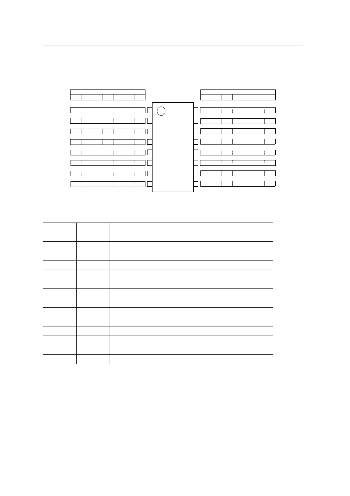
PINOUT
(Top view)
MO ×
SM8707 series
DE FGHKL
MO1
MO2 MO2
SM8707
VDD1
VSS1
MO1 MO1 MO1 MO1
MO2 SO1
NC1NC1
VDD2
VSS2
XTI
XTO
NC1
1
MO1
MO2
8
PIN DESCRIPTION
Name I/O Description
O Video system output
AO ×
SO ×
FSEL I Sampling frequency select
XTI I Crystal oscillator connection or external clock input
XTO O Crystal oscillator connection
VDD1 – Supply for digital block
VSS1 – Ground for digital block
VDD2 – Supply for analog block
VSS2 – Ground for analog block
VDD3 – Supply for digital block
VSS3 – Ground for digital block
NC1 O No connection output (leave pin open circuit)
NC2 I No connection (leave pin open circuit or connect to VDD)
O Audio system output
O Signal processor system output
16
L
SO2
FSELFSEL FSEL FSEL FSEL FSEL
SO1
AO2
AO1 AO1
SO2
AO1
9
SM8707
NC1
NC2
SO2
SO3SO3
VDD3
VSS3
SO2
SO1 SO1
NC2
SO2
AO2 AO2 AO2
AO1 AO1 AO1
DEFGHK
SO2SO4 SO3
SO2
SO1SO1SO1
NIPPON PRECISION CIRCUITS INC.—2

BLOCK DIAGRAM
SM8707 series
FSEL (NC: SM8707G)
XTI
XTO
X'tal
OSC
Reference
Divider 0
Reference
Divider 1
Phase
Detector 0
Loop
Divider 0
Phase
Detector 1
Loop
Divider 1
Charge
Pump 0
Charge
Pump 1
LPF 0 VCO 0
LPF 1 VCO 1
Control
Logic
AO (NC: SM8707G)
SO
MO (NC: SM8707K)
NIPPON PRECISION CIRCUITS INC.—3

−
−
+
−
+
−
° C
° C
°
SM8707 series
Note: Unless otherwise noted, VDD applies to VDD1, VDD2, and VDD3. Similarly, VSS applies to VSS1,
VSS2, and VSS3.
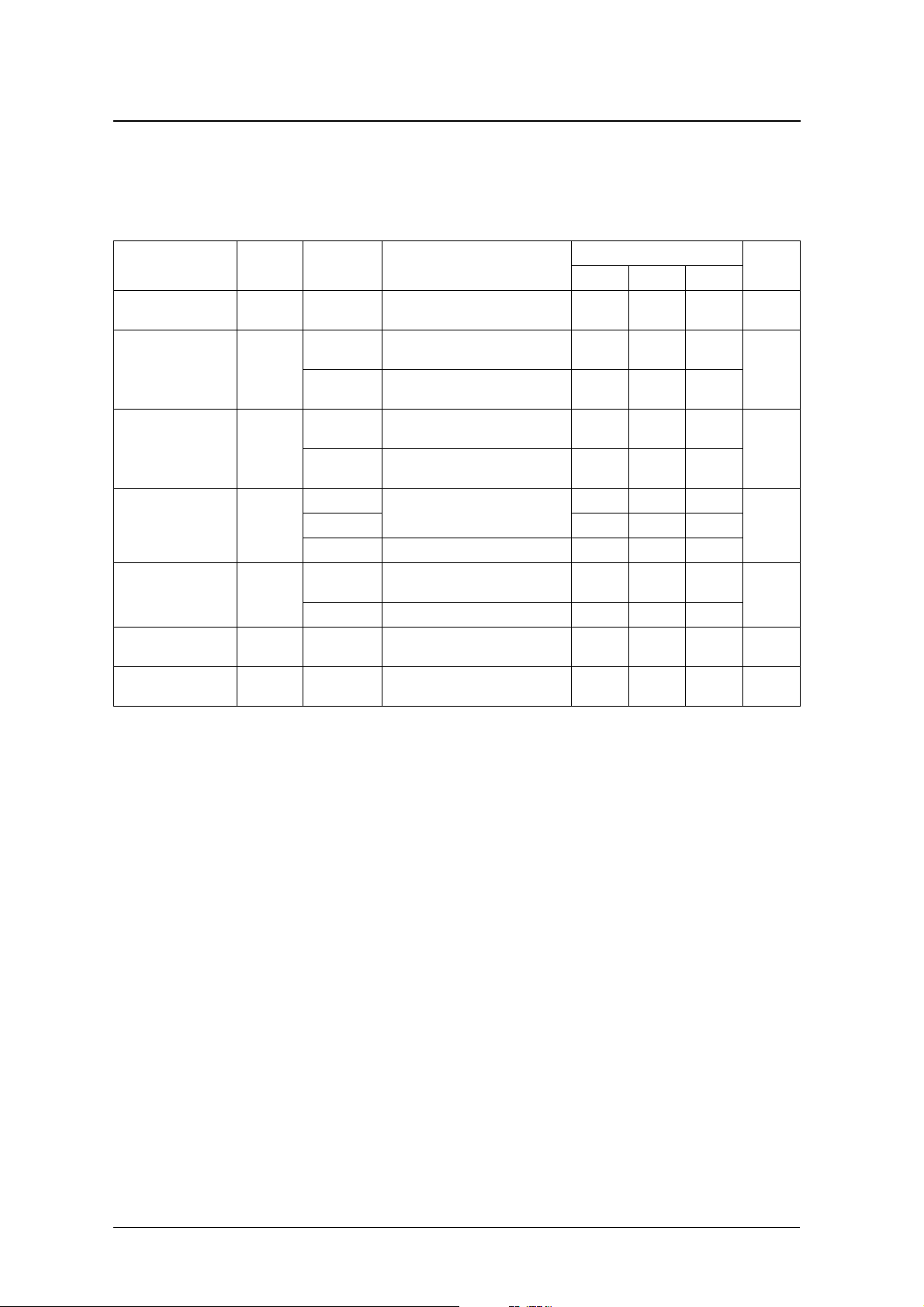
SPECIFICATIONS
Absolute Maximum Ratings
Parameter Symbol Condition Rating Unit
Supply voltage range V
Supply voltage deviation
Input voltage range V
Output voltage range V
Power dissipation P
Storage temperature range T
DD1
V
V
, V
, V
DD2
DD3
– V
– V
– V
OUT
,
DD2
,
DD3
DD3
IN
D
stg
DD1
DD1
V
DD2
0.3 to + 6.5 V
± 0.1 V
0.3 to V
0.3 to V
0.3 V
DD
0.3 V
DD
165 mW
55 to + 125
Recommended Operating Conditions
V
= V
SS
Note 1: The supply voltage is defined relative to V
Note 2:The supply voltages applied on VDD1, VDD2, and VDD3 should be derived from a common supply
Note 3: If the supply voltages on VDD1, VDD2, and VDD3 are from different sources, they should be applied
SM8707D
Supply voltage ranges V
Output load capacitance 1 C
Output load capacitance 2 C
Master clock frequency f
Operating temperature range T
SM8707E
Supply voltage ranges V
Output load capacitance 1 C
Output load capacitance 2 C
Output load capacitance 3 C
Master clock frequency f
Operating temperature range T
= V
SS1
SS2
= V
= 0V unless otherwise noted.
SS3
SS
= 0V.
source.
simultaneously. The SM8707 may be damaged if the supply voltage timing is different.
Parameter Symbol Condition
, V
DD1
DD2
XTAL
opr
, V
L1
L2
(Note 1, 2, 3) + 3.0 – + 3.6 V
DD3
MO1, MO2, SO1, SO2 outputs – – 25 pF
AO1, AO2 outputs – – 15 pF
When using crystal oscillator – 27.0000 – MHz
Parameter Symbol Condition
, V
DD1
DD2
XTAL
opr
, V
L1
L2
L3
(Note 1, 2, 3) + 3.0 – + 3.6 V
DD3
MO1 output – – 40 pF
MO2 output – – 25 pF
SO1, SO2, AO1, AO2 outputs – – 15 pF
When using crystal oscillator – 27.0000 – MHz
min typ max
– 40 – + 85
min typ max
– 10 – + 75
Rating
Rating
Unit
Unit
C
NIPPON PRECISION CIRCUITS INC.—4

SM8707F
SM8707 series
° C
° C
° C
° C
°
Parameter Symbol Condition
Supply voltage ranges V
DD1
Output load capacitance 1 C
Output load capacitance 2 C
Master clock frequency f
Operating temperature range T
SM8707G
Parameter Symbol Condition
Supply voltage ranges V
DD1
Output load capacitance 1 C
Output load capacitance 2 C
Output load capacitance 3 C
Master clock frequency f
Operating temperature range T
SM8707H
Rating
min typ max
, V
DD2
XTAL
opr
, V
L1
L2
(Note 1, 2, 3) + 3.0 – + 3.6 V
DD3
MO1, SO1, SO2 outputs – – 25 pF
AO1, AO2 outputs – – 15 pF
When using crystal oscillator – 27.0000 – MHz
– 40 – + 85
Rating
min typ max
, V
DD2
XTAL
opr
, V
L1
L2
L3
(Note 1, 2, 3) + 3.0 – + 3.6 V
DD3
MO1 output – – 40 pF
SO3 output – – 25 pF
SO1, SO2 outputs – – 15 pF
When using crystal oscillator – 27.0000 – MHz
– 10 – + 75
Unit
Unit
Parameter Symbol Condition
Supply voltage ranges V
DD1
Output load capacitance 1 C
Output load capacitance 2 C
Master clock frequency f
Operating temperature range T
SM8707K
Parameter Symbol Condition
Supply voltage ranges V
DD1
Output load capacitance C
Master clock frequency f
Operating temperature range T
SM8707L
Parameter Symbol Condition
Supply voltage ranges V
Output load capacitance C
Master clock frequency f
Operating temperature range T
DD1
Rating
min typ max
, V
DD2
XTAL
opr
, V
L1
L2
(Note 1, 2, 3) + 3.0 – + 3.6 V
DD3
MO1, MO2, SO2, SO3 outputs – – 25 pF
AO1, SO1 outputs – – 15 pF
When using crystal oscillator – 27.0000 – MHz
– 40 – + 85
Rating
min typ max
, V
DD2
XTAL
opr
, V
L
(Note 1, 2, 3) + 3.0 – + 3.6 V
DD3
Outputs – – 25 pF
When using crystal oscillator – 27.0000 – MHz
– 40 – + 85
Rating
min typ max
, V
DD2
XTAL
opr
, V
L
(Note 1, 2, 3) + 3.0 – + 3.6 V
DD3
Outputs excluding XTO – – 15 pF
When using crystal oscillator – 27.0000 – MHz
– 40 – + 85
Unit
Unit
Unit
C
NIPPON PRECISION CIRCUITS INC.—5

DC Electrical Characteristics
■
SM8707D/F/H/K/L
f
XTAL
■
SM8707E/G
f
XTAL
= 27.0000MHz, V
= 27.0000MHz, V
= 3.3V ± 0.3V, V
DD
= 3.3V ± 0.3V, V
DD
SM8707 series
= 0V, Ta = – 40 to + 85 ° C unless otherwise noted.
SS
= 0V, Ta = – 10 to + 75 ° C unless otherwise noted.
SS
Parameter Symbol Pins Condition
Current
consumption
Input voltage
Input current
Output voltage
= 3.3V, Ta = 25 ° C,
DD
I
VDD
DD
fs = 48kHz, Crystal
oscillator connected,
no load on all outputs
V
IH
FSEL, XTI V
V
IL
I
IH1
I
IL1
I
IH2
I
IL2
V
OH
V
OL
1
FSEL
XTI
All outputs
excluding XTO
= 3.3V
DD
VIN = V
DD
VIN = 0V – 100 – −
VIN = V
DD
VIN = 0V – 40 – −
I
= − 2mA VDD − 0.4 – –
OH
IOL = 2mA – – 0.4
Excluding
SM8707G
SM8707G – 20 27
V
1. FSEL pin has Schmitt-trigger input and built-in pull-up resistor (SM8707G: NC pin).
Rating
min typ max
–3545
0.8 V
DD
– – 0.2 V
––
DD
––1
––40
Unit
mA
V
µA
V
NIPPON PRECISION CIRCUITS INC.—6
SM8707 series
AC Electrical Characteristics
SM8707D
f
= 27.0000MHz, VDD = 3.3V ± 0.3V, VSS = 0V, Ta = – 40 to + 85 °C unless otherwise noted.
XTAL
Parameter Symbol Pins Condition
Unit
min typ max
Rating
External input clock
1
frequency
Output clock rise time
Output clock fall time
Output clock jitter
3
Output clock duty cycle
Settling time
Power-up time
2
2, 4
f
2
2
t
(1-sigma)
2
XTI Applies to external clock input use only – 27.0000 – MHz
XTI
MO1, MO2,
SO1, SO2
t
r
AO1, AO2
MO1, MO2,
SO1, SO2
t
f
AO1, AO2
MO1, MO2
jitter
AO1, AO2 Ta = 25°C, CL = 15pF, VO = 0.5V
MO1, MO2,
SO1, SO2
Dt
AO1, AO2 Ta = 25°C, C
All outputs
t
S
excluding XTO
All outputs
t
P
excluding XTO
CL = 25 pF, transition between VOL =
0.2VDD and VOH = 0.8V
= 15pF, transition between
C
L
V
= 0.2VDD and VOH = 0.8V
OL
DD
DD
CL = 25pF, transition between VOH =
0.8VDD and VOL = 0.2V
= 15pF, transition between
C
L
VOH = 0.8VDD and VOL = 0.2V
Ta = 25°C, C
Ta = 25°C, C
L
L
L
DD
= 25pF, VO = 0.5V
= 25pF, VO = 0.5V
=15 pF, VO = 0.5V
DD
DD
DD
DD
DD
– 2.0 –
– 2.0 –
– 2.0 –
– 2.0 –
–20–
–70–
45 50 55
45 50 55
––1µs
–15ms
ns
ns
psSO1, SO2 – 70 –
%
1. When using an external clock input, the XTI duty should be 50% with 3.3V clock signal amplitude level. The input signal voltage should not exceed the
absolute maximum rating, otherwise damage may occur.
2. The numeric values are measured values obtained using the circuit in Figure 1 and the NPC standard evaluation board.
3. The numeric values are measured values obtained using the circuit in Figure 2 and the NPC standard evaluation board.
4. This is the time, after the supply is turned ON from the OFF state, until the output clock reaches ± 0.1% of the specified frequency.
NIPPON PRECISION CIRCUITS INC.—7

SM8707 series
SM8707E
f
= 27.0000MHz, VDD = 3.3V ± 0.3V, VSS = 0V, Ta = – 10 to + 75 °C unless otherwise noted.
XTAL
Parameter Symbol Pins Condition
External input clock
1
frequency
Output clock rise time
Output clock fall time
f
2
2
XTI Applies to external clock input use only – 27.0000 – MHz
XTI
= 40 pF, transition between VOL =
C
MO1
t
r
SO1, SO2,
AO1, AO2
MO1
t
f
SO1, SO2,
AO1, AO2
L
0.2VDD and VOH = 0.8V
= 25 pF, transition between VOL =
C
L
0.2VDD and VOH = 0.8V
C
= 15pF, transition between VOL =
L
0.2VDD and VOH = 0.8V
= 40pF, transition between VOH =
C
L
0.8VDD and VOL = 0.2V
= 25pF, transition between VOH =
C
L
0.8VDD and VOL = 0.2V
C
= 15pF, transition between VOH =
L
0.8VDD and VOL = 0.2V
MO1 Ta = 25°C, CL = 40pF, VO = 0.5V
Output clock jitter
3
t
(1-sigma)
MO2 Ta = 25°C, CL = 25pF, VO = 0.5V
jitter
SO1, SO2,
AO1, AO2
Ta = 25°C, C
MO1 Ta = 25°C, C
Output clock duty cycle
Settling time
Power-up time
2
2, 4
2
MO2 Ta = 25°C, CL = 25pF, VO = 0.5V
Dt
SO1, SO2,
AO1, AO2
t
AO1, AO2 – – 1 µs
S
All outputs
t
P
excluding XTO
Ta = 25°C, C
DD
DD
DD
DD
DD
DD
= 15pF, VO = 0.5V
L
= 40pF, VO = 0.5V
L
=15 pF, VO = 0.5V
L
min typ max
– 2.0 –
– 2.0 –
– 2.0 –
– 2.0 –
– 2.0 –
– 2.0 –
DD
DD
DD
DD
DD
DD
–20–
–20–
–55–
45 50 55
45 50 55
45 50 55
–15ms
Unit
nsMO2
nsMO2
ps
%
1. When using an external clock input, the XTI duty should be 50% with 3.3V clock signal amplitude level. The input signal voltage should not exceed the
absolute maximum rating, otherwise damage may occur.
2. The numeric values are measured values obtained using the circuit in Figure 1 and the NPC standard evaluation board.
3. The numeric values are measured values obtained using the circuit in Figure 2 and the NPC standard evaluation board.
4. This is the time, after the supply is turned ON from the OFF state, until the output clock reaches ± 0.1% of the specified frequency.
Rating
NIPPON PRECISION CIRCUITS INC.—8

SM8707 series
SM8707F
f
= 27.0000MHz, VDD = 3.3V ± 0.3V, VSS = 0V, Ta = – 40 to + 85 °C unless otherwise noted.
XTAL
Parameter Symbol Pins Condition
External input clock
1
frequency
Output clock rise time
Output clock fall time
f
2
2
XTI Applies to external clock input use only – 27.0000 – MHz
XTI
MO1, SO1,
SO2
t
r
AO1, AO2
MO1, SO1,
SO2
t
f
AO1, AO2
CL = 25 pF, transition between VOL =
0.2VDD and VOH = 0.8V
= 15pF, transition between
C
L
VOL = 0.2VDD and VOH = 0.8V
CL = 25pF, transition between VOH =
0.8VDD and VOL = 0.2V
= 15pF, transition between
C
L
VOH = 0.8VDD and VOL = 0.2V
MO1
Output clock jitter
3
t
jitter
(1-sigma)
Ta = 25°C, C
AO1, AO2 Ta = 25°C, CL = 15pF, VO = 0.5V
Output clock duty cycle
MO1, SO1,
2
SO2
Dt
Ta = 25°C, CL = 25pF, VO = 0.5V
AO1, AO2 Ta = 25°C, C
Settling time
Power-up time
2
2, 4
t
S
t
P
All outputs
excluding XTO
All outputs
excluding XTO
DD
DD
= 25pF, VO = 0.5V
L
=15 pF, VO = 0.5V
L
min typ max
– 2.0 –
DD
– 2.0 –
– 2.0 –
DD
– 2.0 –
–20–
DD
DD
DD
DD
–40–
45 50 55
45 50 55
––1µs
–15ms
Unit
ns
ns
psSO1, SO2 – 40 –
%
1. When using an external clock input, the XTI duty should be 50% with 3.3V clock signal amplitude level. The input signal voltage should not exceed the
absolute maximum rating, otherwise damage may occur.
2. The numeric values are measured values obtained using the circuit in Figure 1 and the NPC standard evaluation board.
3. The numeric values are measured values obtained using the circuit in Figure 2 and the NPC standard evaluation board.
4. This is the time, after the supply is turned ON from the OFF state, until the output clock reaches ± 0.1% of the specified frequency.
Rating
NIPPON PRECISION CIRCUITS INC.—9

SM8707 series
SM8707G
f
= 27.0000MHz, VDD = 3.3V ± 0.3V, VSS = 0V, Ta = – 10 to + 75 °C unless otherwise noted.
XTAL
Parameter Symbol Pins Condition
External input clock
1
frequency
Output clock rise time
Output clock fall time
f
2
2
XTI Applies to external clock input use only – 27.0000 – MHz
XTI
= 40 pF, transition between VOL =
C
MO1
t
r
SO1, SO2
MO1
t
f
SO1, SO2
L
0.2VDD and VOH = 0.8V
= 25 pF, transition between VOL =
C
L
0.2VDD and VOH = 0.8V
= 15pF, transition between VOL =
C
L
0.2VDD and VOH = 0.8V
= 40pF, transition between VOH =
C
L
0.8VDD and VOL = 0.2V
= 25pF, transition between VOH =
C
L
0.8VDD and VOL = 0.2V
= 15pF, transition between VOH =
C
L
0.8VDD and VOL = 0.2V
MO1 Ta = 25°C, C
Output clock jitter
3
t
jitter
(1-sigma)
SO1, SO2 Ta = 25°C, CL = 15pF, VO = 0.5V
MO1 Ta = 25°C, CL = 40pF, VO = 0.5V
Output clock duty cycle
2
Dt
SO1, SO2 Ta = 25°C, CL =15 pF, VO = 0.5V
Power-up time
2, 4
t
P
All outputs
excluding XTO
DD
DD
DD
DD
DD
DD
= 40pF, VO = 0.5V
L
min typ max
– 2.0 –
– 2.0 –
– 2.0 –
– 2.0 –
– 2.0 –
– 2.0 –
DD
DD
DD
DD
DD
DD
–20–
–40–
–40–
45 50 55
45 50 55
45 50 55
–15ms
Unit
nsSO3
nsSO3
psSO3 Ta = 25°C, CL = 25pF, VO = 0.5V
%SO3 Ta = 25°C, CL = 25pF, VO = 0.5V
1. When using an external clock input, the XTI duty should be 50% with 3.3V clock signal amplitude level. The input signal voltage should not exceed the
absolute maximum rating, otherwise damage may occur.
2. The numeric values are measured values obtained using the circuit in Figure 1 and the NPC standard evaluation board.
3. The numeric values are measured values obtained using the circuit in Figure 2 and the NPC standard evaluation board.
4. This is the time, after the supply is turned ON from the OFF state, until the output clock reaches ± 0.1% of the specified frequency.
Rating
NIPPON PRECISION CIRCUITS INC.—10

SM8707 series
SM8707H
f
= 27.0000MHz, VDD = 3.3V ± 0.3V, VSS = 0V, Ta = – 40 to + 85 °C unless otherwise noted.
XTAL
Parameter Symbol Pins Condition
External input clock
1
frequency
Output clock rise time
Output clock fall time
f
2
2
XTI Applies to external clock input use only – 27.0000 – MHz
XTI
t
t
MO1, MO2,
SO2, SO3
r
SO1, AO1
MO1, MO2,
SO2, SO3
f
SO1, AO1
CL = 25 pF, transition between VOL =
0.2VDD and VOH = 0.8V
= 15pF, transition between
C
L
VOL = 0.2VDD and VOH = 0.8V
CL = 25pF, transition between VOH =
0.8VDD and VOL = 0.2V
= 15pF, transition between
C
L
VOH = 0.8VDD and VOL = 0.2V
MO1, MO2
Output clock jitter
3
t
jitter
(1-sigma)
Ta = 25°C, C
SO1, AO1 Ta = 25°C, CL = 15pF, VO = 0.5V
Output clock duty cycle
MO1, MO2,
2
SO2, SO3
Dt
Ta = 25°C, CL = 25pF, VO = 0.5V
SO1, AO1 Ta = 25°C, C
Settling time
Power-up time
2
2, 4
t
S
t
P
All outputs
excluding XTO
All outputs
excluding XTO
DD
DD
= 25pF, VO = 0.5V
L
=15 pF, VO = 0.5V
L
min typ max
– 2.0 –
DD
– 2.0 –
– 2.0 –
DD
– 2.0 –
–20–
DD
DD
DD
DD
–70–
45 50 55
45 50 55
––1µs
–15ms
Unit
ns
ns
psSO2, SO3 – 70 –
%
1. When using an external clock input, the XTI duty should be 50% with 3.3V clock signal amplitude level. The input signal voltage should not exceed the
absolute maximum rating, otherwise damage may occur.
2. The numeric values are measured values obtained using the circuit in Figure 1 and the NPC standard evaluation board.
3. The numeric values are measured values obtained using the circuit in Figure 2 and the NPC standard evaluation board.
4. This is the time, after the supply is turned ON from the OFF state, until the output clock reaches ± 0.1% of the specified frequency.
Rating
NIPPON PRECISION CIRCUITS INC.—11

SM8707 series
SM8707K
f
= 27.0000MHz, VDD = 3.3V ± 0.3V, VSS = 0V, Ta = – 40 to + 85 °C unless otherwise noted.
XTAL
Parameter Symbol Pins Condition
External input clock
1
frequency
Frequency deviation
1
Output clock rise time
Output clock fall time
Output clock jitter
3
Output clock duty cycle
Settling time
Power-up time
2
2, 4
f
2
2
t
(1-sigma)
2
XTI Applies to external clock input use only – 27.0000 – MHz
XTI
D
jitter
Dt
t
t
f
t
r
t
f
S
P
SO1, SO2, SO3,
SO4, AO1
SO1, SO2, SO3,
SO4, AO1
SO1, SO2, SO3,
SO4, AO1
SO1, SO2, SO3,
SO4, AO1
SO1, SO2, SO3,
SO4, AO1
All outputs
excluding XTO
All outputs
excluding XTO
Applies to external clock input use only,
When frequency deviation of master
clock is 0ppm
CL = 25 pF, transition between VOL =
0.2VDD and VOH = 0.8V
CL = 25pF, transition between VOH =
0.8VDD and VOL = 0.2V
Ta = 25°C, C
Ta = 25°C, C
DD
DD
= 25pF, VO = 0.5V
L
= 25pF, VO = 0.5V
L
min typ max
–15 – +15 ppm
– 2.0 – ns
– 2.0 – ns
DD
DD
–60–ps
45 50 55 %
––1µs
–15ms
Unit
1. When using an external clock input, the XTI duty should be 50% with 3.3V clock signal amplitude level. The input signal voltage should not exceed the
absolute maximum rating, otherwise damage may occur.
2. The numeric values are measured values obtained using the circuit in Figure 1 and the NPC standard evaluation board.
3. The numeric values are measured values obtained using the circuit in Figure 2 and the NPC standard evaluation board.
4. This is the time, after the supply is turned ON from the OFF state, until the output clock reaches ± 0.1% of the specified frequency.
Rating
NIPPON PRECISION CIRCUITS INC.—12

SM8707 series
SM8707L
f
= 27.0000MHz, VDD = 3.3V ± 0.3V, VSS = 0V, Ta = – 40 to + 85 °C unless otherwise noted.
XTAL
Parameter Symbol Pins Condition
External input clock
1
frequency
Output clock rise time
Output clock fall time
f
2
2
XTI Applies to external clock input use only – 27.0000 – MHz
XTI
t
r
t
f
MO1, MO2, SO1,
SO2, AO1, AO2
MO1, MO2, SO1,
SO2, AO1, AO2
CL = 15 pF, transition between VOL =
0.2VDD and VOH = 0.8V
CL = 15pF, transition between VOH =
0.8VDD and VOL = 0.2V
MO1, MO2
Output clock jitter
3
t
jitter
(1-sigma)
SO1, SO2,
Ta = 25°C, C
AO1, AO2
Output clock duty cycle
Settling time
Power-up time
2
2, 4
2
Dt
t
S
t
P
MO1, MO2, SO1,
SO2, AO1, AO2
All outputs
excluding XTO
All outputs
excluding XTO
Ta = 25°C, C
DD
DD
= 15pF, VO = 0.5V
L
= 15pF, VO = 0.5V
L
min typ max
– 2.0 – ns
– 2.0 – ns
–20–ps
DD
DD
–60–ps
45 50 55 %
––1µs
–15ms
Unit
1. When using an external clock input, the XTI duty should be 50% with 3.3V clock signal amplitude level. The input signal voltage should not exceed the
absolute maximum rating, otherwise damage may occur.
2. The numeric values are measured values obtained using the circuit in Figure 1 and the NPC standard evaluation board.
3. The numeric values are measured values obtained using the circuit in Figure 2 and the NPC standard evaluation board.
4. This is the time, after the supply is turned ON from the OFF state, until the output clock reaches ± 0.1% of the specified frequency.
Rating
27MHz
DUT
DUT:Device under test
Active Probe
(HP1152A)
Passive Probe
(HP10435A)
Figure 1. Measurement circuit 1
Oscilloscope
(Infinium
HP54845A)
Frequency &
Time Interval
Analyzer
(HP5371A)
27MHz
DUT
DUT:Device under test
Figure 2. Measurement circuit 2
Active Probe
(HP54701A)
Oscilloscope
(HP54720D
+HP54721A)
Jitter
Measurement
System
(ASA, M1)
NIPPON PRECISION CIRCUITS INC.—13

SM8707 series
FUNCTIONAL DESCRIPTION
27MHz Master Clock
The SM8707 series 27MHz master clock circuit is configured, as shown in Figure 3 and 4, with the crystal
oscillator element connected between XTI (pin 7) and XTO (pin 8).
Alternatively, the 27MHz master clock can be supplied from an external master clock input on XTI, as shown
in Figure 5 and 6.
If an external input clock on XTI is used, it is recommended that the frequency be 27.0000MHz, with 50%
duty, and 3.3V voltage amplitude level.
Furthermore, when using an external clock input, the input signal voltage should not exceed the absolute maximum rating, otherwise damage may occur.
C1
XTI (Pin 7)
Oscillator
XTO (Pin 8)
C2
C1, C2 = 5 to 33pF
Figure 3. Crystal oscillator connection
(excluding SM8707K)
External Clock
Open
XTI (Pin 7)
Oscillator
XTO (Pin 8)
Figure 5. External clock input
(excluding SM8707K)
Internal
Circuits
Internal
Circuits
MO
MO
C1
XTI (Pin 7)
Oscillator
XTO (Pin 8)
C2
C1, C2 = 5 to 33pF
Figure 4. Crystal oscillator connection
(SM8707K)
External Clock
Open
XTI (Pin 7)
Oscillator
XTO (Pin 8)
Figure 6. External clock input
(SM8707K)
Internal
Circuits
Internal
Circuits
NIPPON PRECISION CIRCUITS INC.—14

SM8707 series
Sampling Frequency and Output Clock Frequency
SM8707D
The SM8707D sampling frequency fs can be switched between 44.1kHz when FSEL (pin 14) is HIGH, and
48kHz when FSEL is LOW. The audio output (AO1) is a 384fs frequency clock when FSEL is HIGH (fs =
44.1kHz), and 768fs frequency clock when FSEL is LOW (fs = 48kHz) where fs is determined by the setting
on FSEL. The audio output (AO2) is a 512fs frequency clock. In addition, the signal processor output (SO1 and
SO2) is a 16.9344MHz, 33.8688MHz frequency clock derived from the master clock. And the video output
(MO1 and MO2) is a 27MHz frequency clock, identical to the master clock.
The SM8707D possible output clock frequencies are shown in Table 1.
Table 1. Sampling frequency and output clock frequency (27.0000MHz master clock frequency)
FSEL
(Pin 14)
HIGH 44.1
LOW 48
Sampling
frequency fs
[kHz]
AO1 (Pin 9) AO2 (Pin 10) SO1 (Pin 13) SO2 (Pin 15) MO1 (Pin 3) MO2 (Pin 4)
16.9344
(384fs)
36.8640
(768fs)
22.5792
(512fs)
24.5760
(512fs)
Output clock frequency [MHz]
16.9344 33.8688 27.0000 27.0000
16.9344 33.8688 27.0000 27.0000
SM8707E
The SM8707E sampling frequency fs can be switched between 44.1kHz when FSEL (pin 14) is LOW, and
48kHz when FSEL is HIGH. The audio output (AO1 and AO2) is a 512fs frequency clock, where fs is determined by the setting on FSEL. In addition, the signal processor output (SO1 and SO2) is a 33.8688MHz frequency clock derived from the master clock. And the video output (MO1 and MO2) is a 27MHz frequency
clock, identical to the master clock.
The SM8707E possible output clock frequencies are shown in Table 2.
Table 2. Sampling frequency and output clock frequency (27.0000MHz master clock frequency)
FSEL
(Pin 14)
HIGH 48
Sampling
frequency fs
[kHz]
AO1 (Pin 9) AO2 (Pin 10) SO1 (Pin 13) SO2 (Pin 15) MO1 (Pin 3) MO2 (Pin 4)
24.5760
(512fs)
24.5760
(512fs)
Output clock frequency [MHz]
33.8688 33.8688 27.0000 27.0000
LOW 44.1
22.5792
(512fs)
22.5792
(512fs)
33.8688 33.8688 27.0000 27.0000
NIPPON PRECISION CIRCUITS INC.—15

SM8707 series
SM8707F
The SM8707F sampling frequency fs can be switched between 44.1kHz when FSEL (pin 14) is HIGH, and
48kHz when FSEL is LOW. The audio outputs (AO1 and AO2) are equivalent to 768fs, where fs is determined
by the setting on FSEL. In addition, the signal processor outputs (SO1 and SO2) are 16.9344MHz and
33.8688MHz clocks, respectively, derived from the master clock. The video output (MO1) is a 27MHz clock,
identical to the master clock.
The SM8707F supported clock frequencies are shown in Table 3.
Table 3. Sampling frequency and output clock frequency (27.0000MHz master clock frequency)
FSEL
(Pin 14)
HIGH 44.1
LOW 48
Sampling
frequency fs
[kHz]
AO1 (Pin 9) AO2 (Pin 10) SO1 (Pin 13) SO2 (Pin 15) MO1 (Pin 3)
33.8688
(768fs)
36.8640
(768fs)
Output clock frequency [MHz]
33.8688
(768fs)
36.8640
(768fs)
16.9344 33.8688 27.0000
16.9344 33.8688 27.0000
SM8707G
The SM8707G signal processor outputs (SO1, SO2 and SO3) are all 33.8688MHz clocks, derived from the
master clock. The video output (MO1) is a 27MHz clock, identical to the master clock.
The SM8707G supported clock frequencies are shown in Table 4.
Table 4. Sampling frequency and output clock frequency (27.0000MHz master clock frequency)
Output clock frequency [MHz]
SO1 (Pin 9) SO2 (Pin 10) SO3 (Pin 13) MO1 (Pin 3)
33.8688 33.8688 33.8688 27.0000
SM8707H
The SM8707H sampling frequency fs can be switched between 44.1kHz when FSEL (pin 14) is HIGH, and
48kHz when FSEL is LOW. The audio output (AO1) is equivalent to 512fs, where fs is determined by the setting on FSEL. In addition, the signal processor outputs (SO1, SO2 and SO3) are 36.8640MHz, 16.9344MHz
and 33.8688MHz clocks, respectively, derived from the master clock. The video outputs (MO1 and MO2) are
27MHz clocks, identical to the master clock.
The SM8707H supported clock frequencies are shown in Table 5.
Table 5. Sampling frequency and output clock frequency (27.0000MHz master clock frequency)
FSEL
(Pin 14)
HIGH 44.1
LOW 48
Sampling
frequency fs
[kHz]
AO1 (Pin 10) SO1 (Pin 9) SO2 (Pin 13) SO3 (Pin 15) MO1 (Pin 3) MO2 (Pin 4)
22.5792
(512fs)
24.5760
(512fs)
36.8640 16.9344 33.8688 27.0000 27.0000
36.8640 16.9344 33.8688 27.0000 27.0000
Output clock frequency [MHz]
NIPPON PRECISION CIRCUITS INC.—16

SM8707 series
SM8707K
The SM8707K sampling frequency fs can be switched between 44.1kHz when FSEL (pin 14) is HIGH, and
48kHz when FSEL is LOW. The audio output (AO1) is equivalent to 768fs, where fs is determined by the setting on FSEL. In addition, the signal processor output (SO1, SO2, SO3 and SO4) is 24.5760MHz,
18.4320MHz, 36.8640MHz and 33.8688MHz clocks, respectively, derived from the master clock. Also, the
audio output AO1 36.8688MHz clock is synchronized with the signal processor output SO4 clock, and audio
output AO1 36.8640MHz clock is synchronized with the signal processor output SO3 clock.
The SM8707K supported clock frequencies are shown in Table 6.
Table 6. Sampling frequency and output clock frequency (27.0000MHz master clock frequency)
FSEL
(Pin 14)
HIGH 44.1
LOW 48
Sampling
frequency fs
[kHz]
AO1 (Pin 10) SO1 (Pin 4) SO2 (Pin 9) SO3 (Pin 13) SO4 (Pin 15)
33.8688
(768fs)
36.8640
(768fs)
Output clock frequency [MHz]
24.5760 18.4320 36.8640 33.8688
24.5760 18.4320 36.8640 33.8688
SM8707L
The SM8707L sampling frequency fs can be switched between 44.1kHz when FSEL (pin 14) is LOW, and
48kHz when FSEL is HIGH. The audio output (AO1 and AO2) is a 768fs frequency clock, where fs is determined by the setting on FSEL. In addition, the signal processor output (SO1 and SO2) is 24.5760MHz and
33.8688MHz frequency clock derived from the master clock. And the video output (MO1 and MO2) is a
27MHz frequency clock, identical to the master clock.
The SM8707L supported clock frequencies are shown in Table 7.
Table 7. Sampling frequency and output clock frequency (27.0000MHz master clock frequency)
FSEL
(Pin 14)
HIGH 44.1
Sampling
frequency fs
[kHz]
AO1 (Pin 9) AO2 (Pin 10) SO1 (Pin 13) SO2 (Pin 15) MO1 (Pin 3) MO2 (Pin 4)
33.8688
(768fs)
33.8688
(768fs)
Output clock frequency [MHz]
24.5760 33.8688 27.0000 27.0000
LOW 48
36.8640
(768fs)
36.8640
(768fs)
24.5760 33.8688 27.0000 27.0000
NIPPON PRECISION CIRCUITS INC.—17

SM8707 series
Spike Noise Prevention Function
All device versions, excluding the SM8707G which has no FSEL input, have a spike noise prevention circuit
that prevents any spike noise generation in the audio output clocks when the sampling frequency is switched
using FSEL.
The state of the AO× output before and after FSEL is switched is shown in Figure 7.
When FSEL is switched, either from LOW to HIGH or HIGH to LOW, the spike noise prevention circuit stops
the AO× clock output by a maximum of 1µs, and then the output clock changes to reflect the current FSEL setting.
fs = 44.1kHz
(SM8707E: fs = 48kHz)
fs = 48kHz
(SM8707E: fs = 44.1kHz)
FSEL
AO
1µs (max)
Figure 7. Spike noise prevention circuit timing at sampling frequency switching
Sampling Frequency Switching Settling Time
The clock output response when the sampling frequency is switched using FSEL is shown in Figure 8. Note
that all device versions, excluding the SM8707G which has no FSEL input, have a spike noise prevention circuit which stops the output AO× clocks for a fixed interval, which means the settling time is a maximum 1µs
when the sampling frequency is switched.
0.8V
FSEL
AO
DD
t
S
fs = 48kHz
(SM8707E: fs = 44.1kHz)
fs = 44.1kHz
(SM8707E: fs = 48kHz)
0.2V
DD
t
S
fs = 48kHz
(SM8707E: fs = 44.1kHz)
MO
SO
27.0000MHz
16.9344/33.8688MHz (SM8707D/F)
33.8688MHz (SM8707E)
16.9344/33.8688/36.8640MHz (SM8707H)
18.4320/24.5760/33.8688/36.8640MHz (SM8707K)
24.5760/33.8688MHz (SM8707L)
Figure 8. Output signal switching timing
NIPPON PRECISION CIRCUITS INC.—18

SM8707 series
SM8707 series OUTPUT FREQUENCY LISTING
Version
SM8707D
SM8707E
SM8707F
FSEL polarity
(Pin 14)
H 44.1 27.0000 27.0000
L 48.0 27.0000 27.0000
Output load capacitance [pF] 25 25 15 15 25 25
Pin name MO1 MO2 AO1 AO2 SO1 SO2
H 48.0 27.0000 27.0000
L 44.1 27.0000 27.0000
Output load capacitance [pF] 40 25 15 15 15 15
Pin name MO1 MO2 AO1 AO2 SO1 SO2
H 44.1 27.0000
L 48.0 27.0000
Output load capacitance [pF] 25 − 15 15 25 25
Sampling
frequency
fs [kHz]
Pin 3 Pin 4 Pin 9 Pin 10 Pin 13 Pin 15
Output clock frequency [MHz]
16.9344
(384fs)
36.8640
(768fs)
24.5760
(512fs)
22.5792
(512fs)
33.8688
(768fs)
−
36.8640
(768fs)
22.5792
(512fs)
24.5760
(512fs)
24.5760
(512fs)
22.5792
(512fs)
33.8688
(768fs)
36.8640
(768fs)
16.9344 33.8688
16.9344 33.8688
33.8688 33.8688
33.8688 33.8688
16.9344 33.8688
16.9344 33.8688
SM8707G
SM8707H
SM8707K
SM8707L
Pin name MO1 NC1 AO1 AO2 SO1 SO2
−−27.0000 − 33.8688 33.8688 33.8688 −
Output load capacitance [pF] 40 − 15 15 25 −
Pin name MO1 NC1 SO1 SO2 SO3 NC1
H 44.1 27.0000 27.0000 36.8640
L 48.0 27.0000 27.0000 36.8640
Output load capacitance [pF] 25 25 15 15 25 25
Pin name MO1 MO2 SO1 AO1 SO2 SO3
H 44.1
−
L 48.0 24.5760 18.4320
Output load capacitance [pF] − 25 25 25 25 25
Pin name NC1 SO1 SO2 AO1 SO3 SO4
H 44.1 27.0000 27.0000
L 48.0 27.0000 27.0000
24.5760 18.4320
33.8688
(768fs)
36.8640
(768fs)
22.5792
(512fs)
24.5760
(512fs)
33.8688
(768fs)
36.8640
(768fs)
33.8688
(768fs)
36.8640
(768fs)
16.9344 33.8688
16.9344 33.8688
36.8640 33.8688
36.8640 33.8688
24.5760 33.8688
24.5760 33.8688
Output load capacitance [pF] 15 15 15 15 15 15
Pin name MO1 MO2 AO1 AO2 SO1 SO2
NIPPON PRECISION CIRCUITS INC.—19

SM8707 series
Please pay your attention to the following points at time of using the products shown in this document.
The products shown in this document (hereinafter “Products”) are not intended to be used for the apparatus that exerts harmful influence on
human lives due to the defects, failure or malfunction of the Products. Customers are requested to obtain prior written agreement for such
use from NIPPON PRECISION CIRCUITS INC. (hereinafter “NPC”). Customers shall be solely responsible for, and indemnify and hold NPC
free and harmless from, any and all claims, damages, losses, expenses or lawsuits, due to such use without such agreement. NPC reserves
the right to change the specifications of the Products in order to improve the characteristic or reliability thereof. NPC makes no claim or
warranty that the contents described in this document dose not infringe any intellectual property right or other similar right owned by third
parties. Therefore, NPC shall not be responsible for such problems, even if the use is in accordance with the descriptions provided in this
document. Any descriptions including applications, circuits, and the parameters of the Products in this document are for reference to use the
Products, and shall not be guaranteed free from defect, inapplicability to the design for the mass-production products without further testing
or modification. Customers are requested not to export or re-export, directly or indirectly, the Products to any country or any entity not in
compliance with or in violation of the national export administration laws, treaties, orders and regulations. Customers are requested
appropriately take steps to obtain required permissions or approvals from appropriate government agencies.
NIPPON PRECISION CIRCUITS INC.
4-3, Fukuzumi 2-chome, Koto-ku,
Tokyo 135-8430, Japan
Telephone: +81-3-3642-6661
Facsimile: +81-3-3642-6698
http://www.npc.co.jp/
Email: sales
@npc.co.jp
NC0107CE 2003.12
NIPPON PRECISION CIRCUITS INC.—20
 Loading...