

Page 1
2.7~5.5V
VBG
PGA
Gain = 32, 64, 128
24-bit
ADC
Input
MUX
Digital
Interface
Analog Supply Regulator
Internal
Oscillator
Bandgap Reference
HX711
XI XO
DOUT
PD_SCK
RATE
BASE VSUP DVDD
INB-
INB+
INA-
INA+
To/From
MCU
AVDD
AGND
Load cell
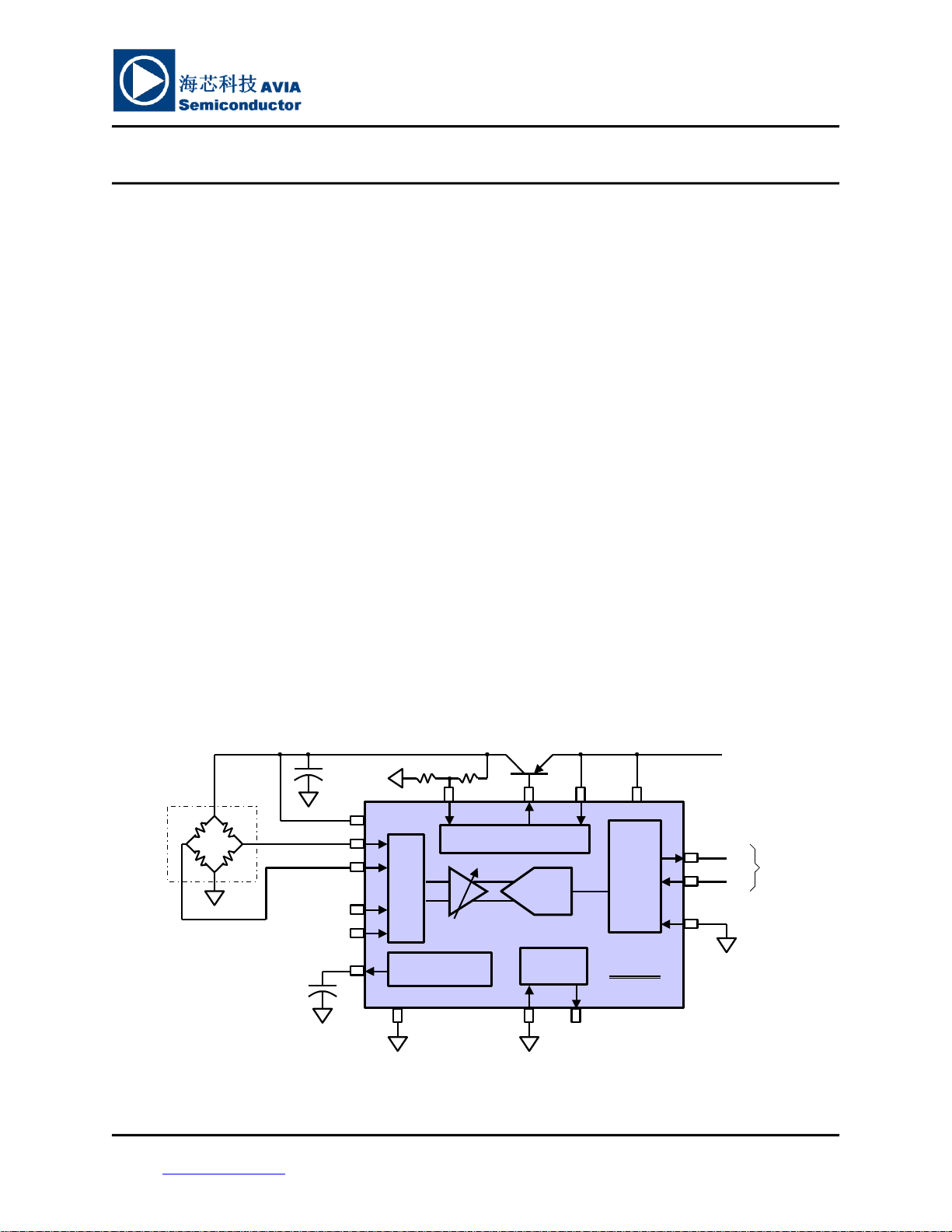
Fig. 1 Typical weigh scale application block diagram
VFB
R2R
1
0.1uF
10uF
S8550
V
AVDD
V
SUP
HX711
24-Bit Analog-to-Digital Converter (ADC) for Weigh Scales
DESCRIPTION
Based on Avia Semiconductor’s patented
technology, HX711 is a precision 24-bit analogto-digital converter (ADC) designed for weigh
scales and industrial control applications to
interface directly with a bridge sensor.
The input multiplexer selects either Channel A
or B differential input to the low-noise
programmable gain amplifier (PGA). Channel A
can be programmed with a gain of 128 or 64,
corresponding to a full-scale differential input
voltage of ±20mV or ±40mV respectively, when
a 5V supply is connected to AVDD analog power
supply pin. Channel B has a fixed gain of 32. Onchip power supply regulator eliminates the need
for an external supply regulator to provide analog
power for the ADC and the sensor. Clock input is
flexible. It can be from an external clock source, a
crystal, or the on-chip oscillator that does not
require any external component. On-chip poweron-reset circuitry simplifies digital interface
initialization.
There is no programming needed for the
internal registers. All controls to the HX711 are
through the pins.
FEATURES
• Two selectable differential input channels
• On-chip active low noise PGA with selectable gain
of 32, 64 and 128
• On-chip power supply regulator for load-cell and
ADC analog power supply
• On-chip oscillator requiring no external
component with optional external crystal
• On-chip power-on-reset
• Simple digital control and serial interface:
pin-driven controls, no programming needed
• Selectable 10SPS or 80SPS output data rate
• Simultaneous 50 and 60Hz supply rejection
• Current consumption including on-chip analog
power supply regulator:
normal operation < 1.5mA, power down < 1uA
• Operation supply voltage range: 2.6 ~ 5.5V
• Operation temperature range: -40 ~ +85℃
• 16 pin SOP-16 package
APPLICATIONS
• Weigh Scales
• Industrial Process Control
Page 2
2
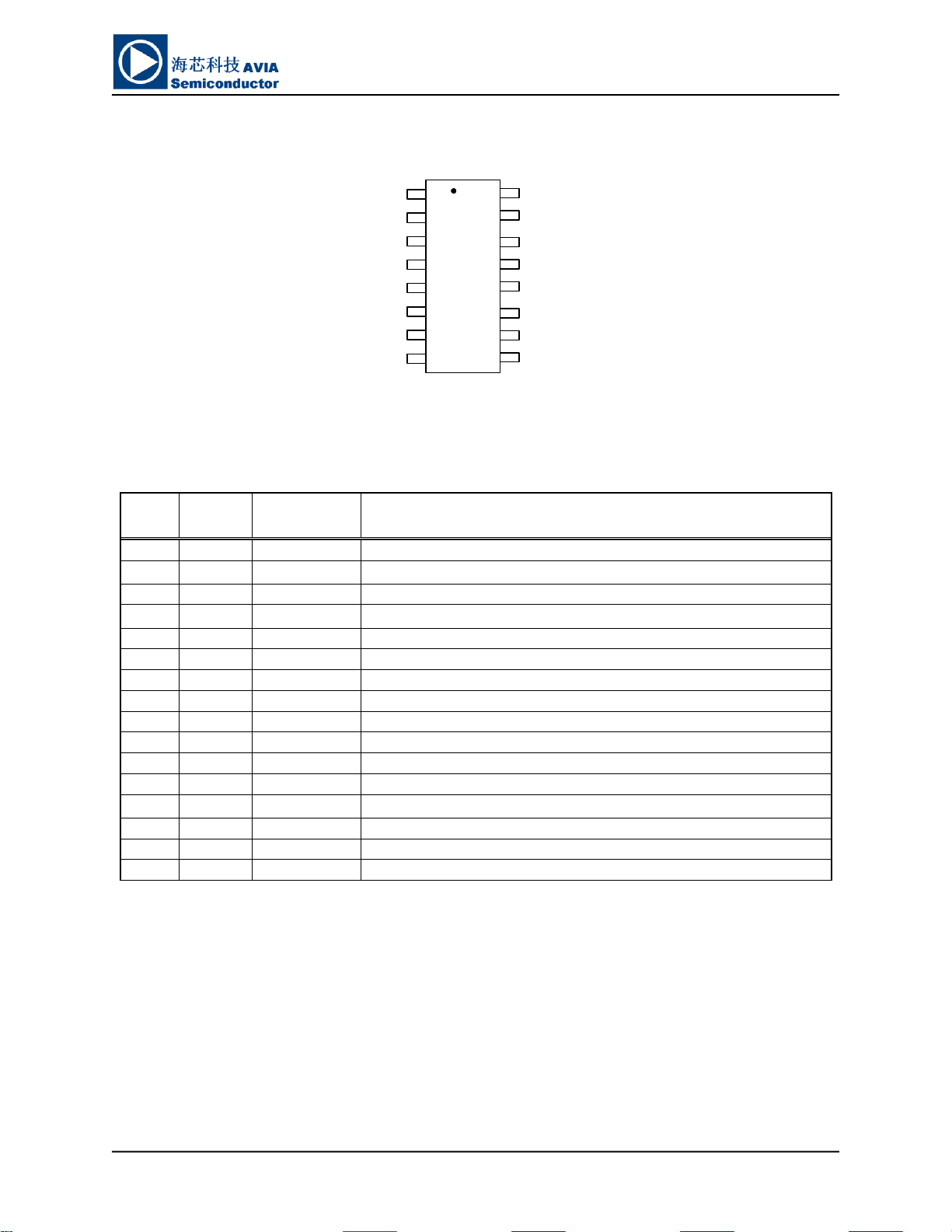
SOP-16L Package
VSUP
Analog Ground
BASE
Analog Power AVDD
Ch. A Negative Input
VFB
Ch. A Positive Input
AGND
Regulator Power
VBG
Regulator Control Output
INNA
INPA
Output Data Rate Control Input
Crystal I/O and External Clock Input
DVDD
RATE
XI
XO
DOUT
PD_SCK
INPB
INNB
1
2
3
4
5
6
7
8
16
15
14
13
12
11
10
9
Regulator Control Input
Reference Bypass
Ch. B Negative Input
Ch. B Positive Input
Serial Data Output
Power Down and Serial Clock Input
Digital Power
Crystal I/O
Pin #
Name
Function
Description
1
VSUP
Power
Regulator supply: 2.7 ~ 5.5V
2
BASE
Analog Output
Regulator control output(NC when not used)
3
AVDD
Power
Analog supply: 2.6 ~ 5.5V
4
VFB
Analog Input
Regulator control input(connect to AGND when not used)
5
AGND
Ground
Analog Ground
6
VBG
Analog Output
Reference bypass output
7
INA-
Analog Input
Channel A negative input
8
INA+
Analog Input
Channel A positive input
9
INB-
Analog Input
Channel B negative input
10
INB+
Analog Input
Channel B positive input
11
PD_SCK
Digital Input
Power down control (high active) and serial clock input
12
DOUT
Digital Output
Serial data output
13
XO
Digital I/O
Crystal I/O (NC when not used)
14
XI
Digital Input
Crystal I/O or external clock input, 0: use on-chip oscillator
15
RATE
Digital Input
Output data rate control, 0: 10Hz; 1: 80Hz
16
DVDD
Power
Digital supply: 2.6 ~ 5.5V
Pin Description
HX711
Table 1 Pin Description
AVIA SEMICONDUCTOR V2.0
Page 3
HX711
3
Parameter
Notes
MIN
TYP
MAX
UNIT
Full scale differential
input range
V(inp)-V(inn)
±0.5(AVDD/GAIN)
V
Common mode input
AGND+1.2
AVDD-1.3
V
Output data rate
Internal Oscillator, RATE = 0
10
Hz
Internal Oscillator, RATE =
DVDD
80
Crystal or external clock,
RATE = 0
f
clk
/1,105,920
Crystal or external clock,
RATE = DVDD
f
clk
/138,240
Output data coding
2’s complement
800000
7FFFFF
HEX
Output settling time
(1)
RATE = 0
400
ms
RATE = DVDD
50
Input offset drift
Gain = 128
0.2
mV
Gain = 64
0.4
Input noise
Gain = 128,RATE = 0
50
nV(rms)
Gain = 128,RATE = DVDD
90
Temperature drift
Input offset(Gain = 128)
±6
nV/℃
Gain(Gain = 128)
±5
ppm/℃
Input common mode
rejection
Gain = 128,RATE = 0
100
dB
Power supply rejection
Gain = 128,RATE = 0
100
dB
Reference bypass
(VBG)
1.25
V
Crystal or external clock
frequency
1
11.0592
20
MHz
Power supply voltage
DVDD
2.6
5.5
V
AVDD,VSUP
2.6
5.5
Analog supply current
(including regulator)
Normal
1400
A
Power down
0.3
Digital supply current
Normal
100
A
Power down
0.2
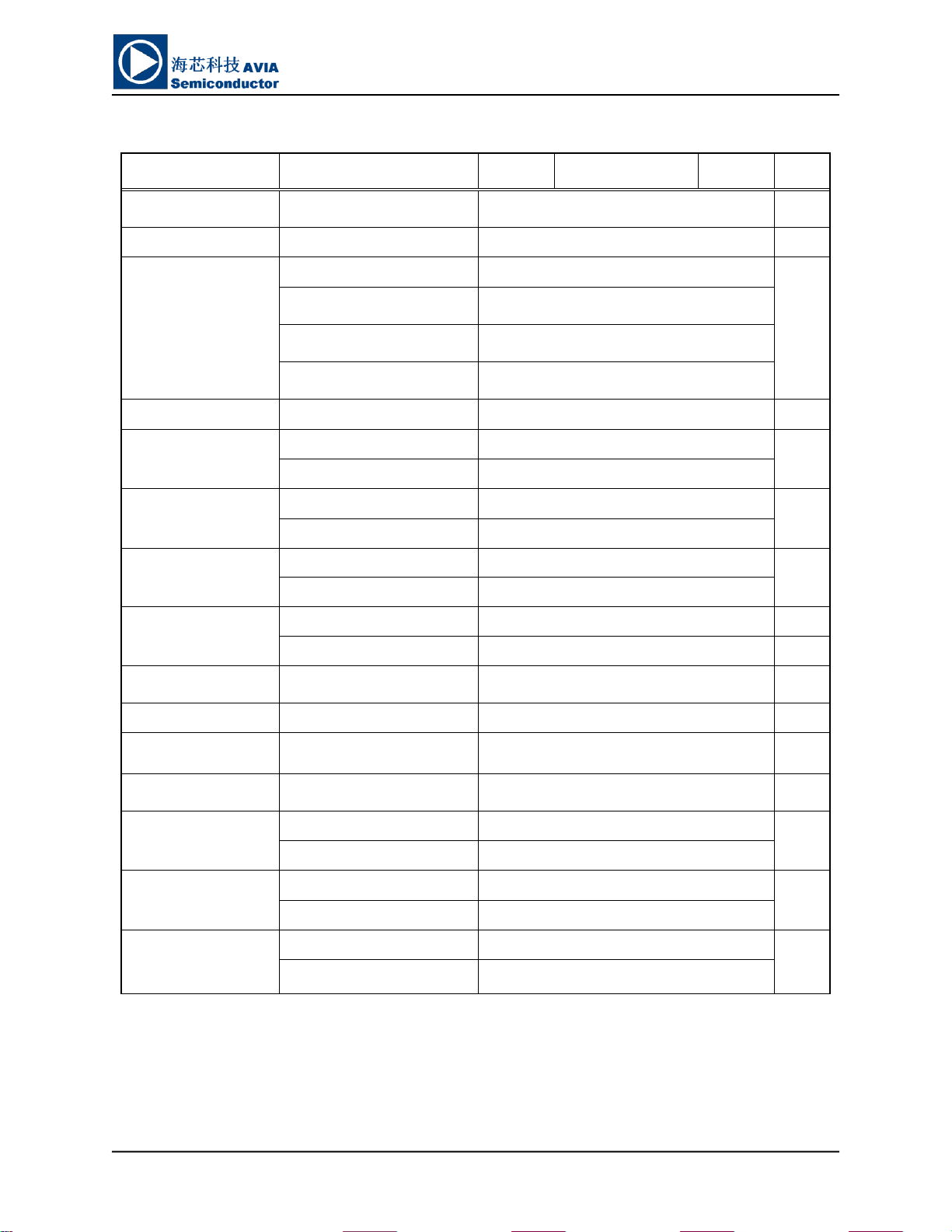
KEY ELECTRICAL CHARACTERISTICS
(1)Settling time refers to the time from power up, reset, input channel change and gain change
to valid stable output data.
AVIA SEMICONDUCTOR V2.0
Table 2 Key Electrical Characteristics
Page 4
4
PD_SCK Pulses
Input
channel
Gain
25
A
128
26
B
32
27
A
64
Analog Inputs
HX711
Channel A differential input is designed to
interface directly with a bridge sensor’s
differential output. It can be programmed with a
gain of 128 or 64. The large gains are needed to
accommodate the small output signal from the
sensor. When 5V supply is used at the AVDD pin,
these gains correspond to a full-scale differential
input voltage of ±20mV or ±40mV respectively.
Channel B differential input has a fixed gain of
32. The full-scale input voltage range is ±80mV,
when 5V supply is used at the AVDD pin.
Power Supply Options
Digital power supply (DVDD) should be the
same power supply as the MCU power supply.
When using internal analog supply regulator,
the dropout voltage of the regulator depends on
the external transistor used. The output voltage is
equal to V
AVDD=VBG
*(R1+R2)/R2 (Fig.1). This
voltage should be designed with a minimum of
100mV below VSUP voltage.
If the on-chip analog supply regulator is not
used, the VSUP pin should be connected to either
AVDD or DVDD, depending on which voltage is
higher. Pin VFB should be connected to Ground
and pin BASE becomes NC. The external 0.1uF
bypass capacitor shown on Fig. 1 at the VBG
output pin is then not needed.
Clock Source Options
By connecting pin XI to Ground, the on-chip
oscillator is activated. The nominal output data
rate when using the internal oscillator is 10
(RATE=0) or 80SPS (RATE=1).
Output Data Rate and Format
When using the on-chip oscillator, output data
rate is typically 10 (RATE=0) or 80SPS
(RATE=1).
When using external clock or crystal, output
data rate is directly proportional to the clock or
crystal frequency. Using 11.0592MHz clock or
crystal results in an accurate 10 (RTE=0) or
80SPS (RATE=1) output data rate.
The output 24 bits of data is in 2’s complement
format. When input differential signal goes out of
the 24-bit range, the output data will be saturated
at 800000h (MIN) or 7FFFFFh (MAX), until the
input signal comes back to the input range.
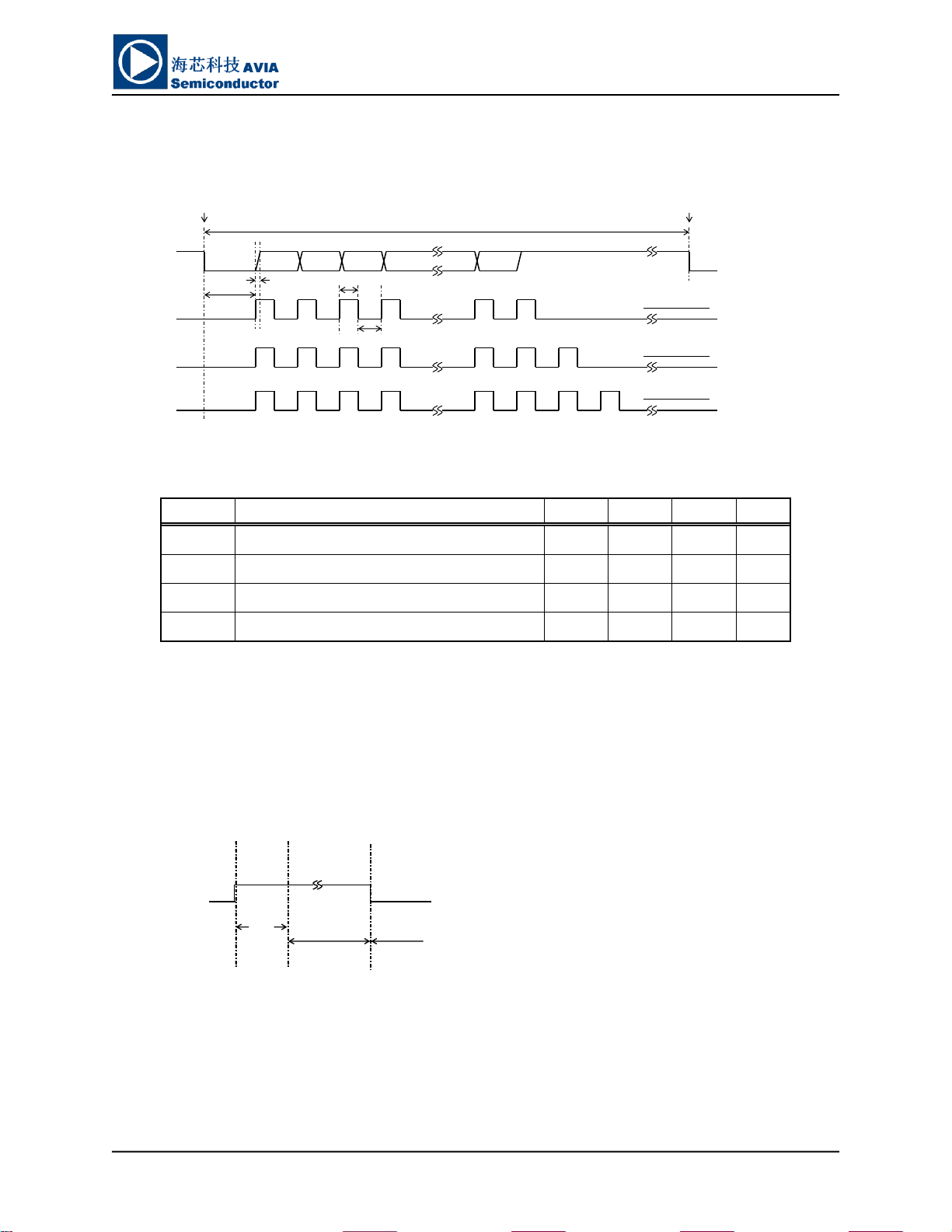
Serial Interface
Pin PD_SCK and DOUT are used for data
retrieval, input selection, gain selection and power
down controls.
When output data is not ready for retrieval,
digital output pin DOUT is high. Serial clock
input PD_SCK should be low. When DOUT goes
to low, it indicates data is ready for retrieval. By
applying 25~27 positive clock pulses at the
PD_SCK pin, data is shifted out from the DOUT
output pin. Each PD_SCK pulse shifts out one bit,
starting with the MSB bit first, until all 24 bits are
shifted out. The 25th pulse at PD_SCK input will
pull DOUT pin back to high (Fig.2).
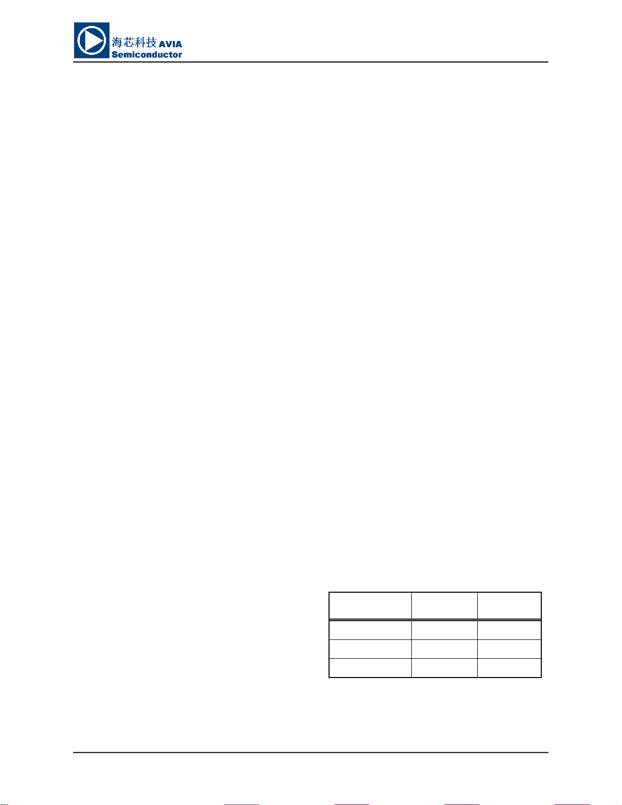
Input and gain selection are controlled by the
number of the input PD_SCK pulses (Table 3).
PD_SCK clock pulses should not be less than 25
or more than 27 within one conversion period, to
avoid causing serial communication error.
If accurate output data rate is needed, crystal or
external reference clock can be used. A crystal
can be directly connected across XI and XO pins.
An external clock can be connected to XI pin,
through a 20pF ac coupled capacitor. This
external clock is not required to be a square wave.
It can come directly from the crystal output pin of
the MCU chip, with amplitude as low as 150 mV.
When using a crystal or an external clock, the
internal oscillator is automatically powered down.
AVIA SEMICONDUCTOR V2.0
Table 3 Input Channel and Gain Selection
Page 5
HX711
5
DOUT
PD_SCK 1 2
MSB LSB
24 25
Next Conversion:CH.A, Gain:128
Current Output Data
Next Output Data
3 4
PD_SCK 1 2 24 25
Next Conversion:CH.B, Gain:32
3 4 26
PD_SCK 1 2 24 25
Next Conversion:CH.A, Gain:64
3 4 26 27
Fig.2 Data output, input and gain selection timing and control
T
1
T
2
T
3
T
4
One conversion period
Symbol
Note
MIN
TYP
MAX
Unit
T1
DOUT falling edge to PD_SCK rising edge
0.1
s
T2
PD_SCK rising edge to DOUT data ready
0.1
s
T3
PD_SCK high time
0.2 1 50
s
T4
PD_SCK low time
0.2 1
s
60s
Power down:
PD_SCK
Power down
Normal
Reset and Power-Down
When chip is powered up, on-chip power on
rest circuitry will reset the chip.
Pin PD_SCK input is used to power down the
HX711. When PD_SCK Input is low, chip is in
normal working mode.
When PD_SCK pin changes from low to high
and stays at high for longer than 60s, HX711
enters power down mode (Fig.3). When internal
regulator is used for HX711 and the external
Fig.3 Power down control
transducer, both HX711 and the transducer will be
powered down. When PD_SCK returns to low,
AVIA SEMICONDUCTOR V2.0
chip will return back to the setup conditions
before power down and enter normal operation
mode.
If PD_SCK pulse number is changed during
the current conversion period, power down should
be executed after current conversion period is
completed. This is to ensure that the change is
saved. When chip returns back to normal
operation from power down, it will return to the
set up conditions of the last change.
Application Example
Fig.1 is a typical weigh scale application using
HX711. It uses on-chip oscillator (XI=0), 10Hz
output data rate (RATE=0). A Single power
supply (2.7~5.5V) comes directly from MCU
power supply. Channel B can be used for battery
level detection. The related circuitry is not shown
on Fig. 1.
Page 6
HX711
6
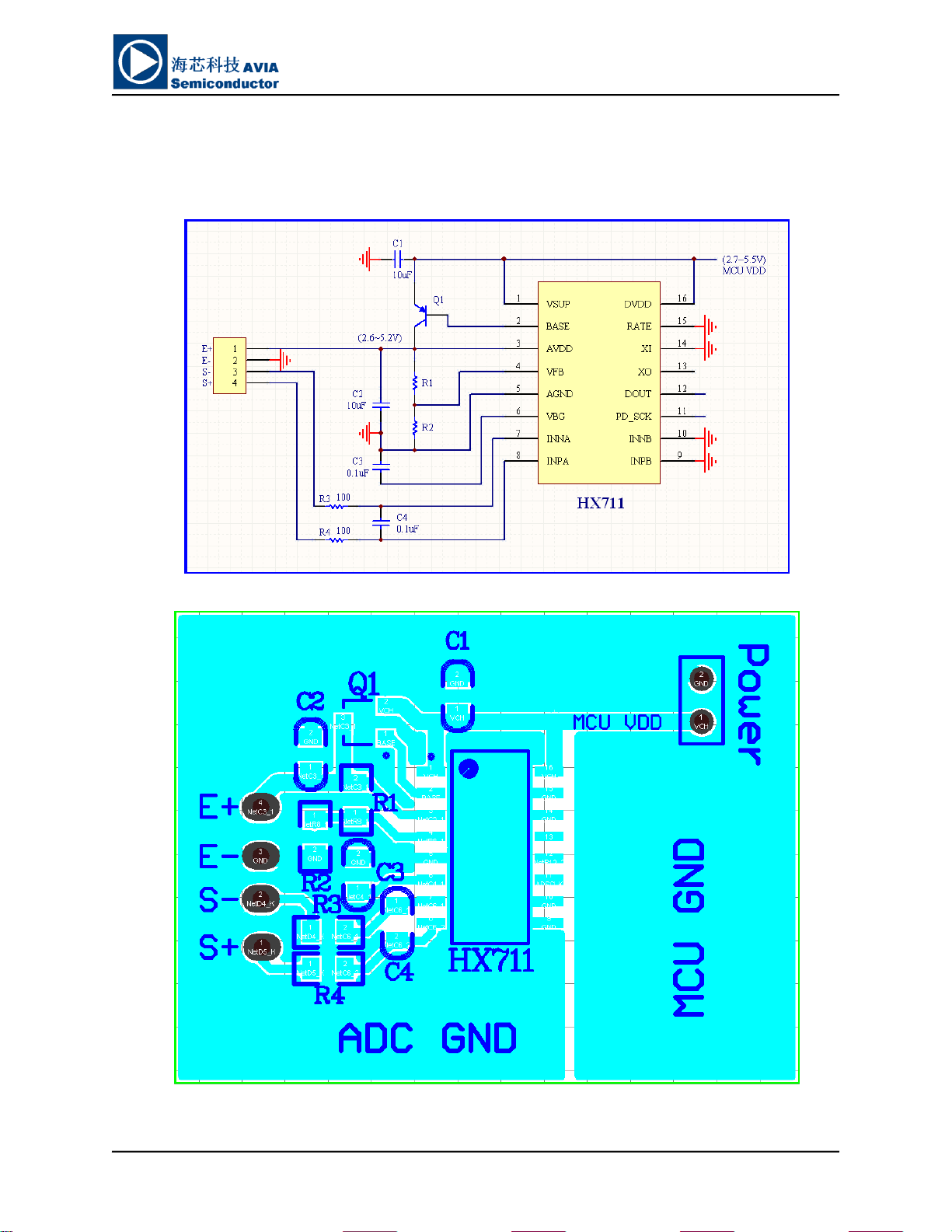
Reference PCB Board (Single Layer)
Fig.4 Reference PCB board schematic
Fig.5 Reference PCB board layout
AVIA SEMICONDUCTOR V2.0
Page 7

HX711
7
Reference Driver (Assembly)
/*------------------------------------------------------------------Call from ASM: LCALL ReaAD
Call from C: extern unsigned long ReadAD(void);
.
.
unsigned long data;
data=ReadAD();
.
.
----------------------------------------------------------------------*/
PUBLIC ReadAD
HX711ROM segment code
rseg HX711ROM
sbit ADDO = P1.5;
sbit ADSK = P0.0;
/*------------------------------------------------- OUT: R4, R5, R6, R7 R7=>LSB
---------------------------------------------------*/
ReadAD:
CLR ADSK //AD Enable(PD_SCK set low)
SETB ADDO //Enable 51CPU I/0
JB ADDO,$ //AD conversion completed?
MOV R4,#24
ShiftOut:
SETB ADSK //PD_SCK set high(positive pulse)
NOP
CLR ADSK //PD_SCK set low
MOV C,ADDO //read on bit
XCH A,R7 //move data
RLC A
XCH A,R7
XCH A,R6
RLC A
XCH A,R6
XCH A,R5
RLC A
XCH A,R5
DJNZ R4,ShiftOut //moved 24BIT?
SETB ADSK
NOP
CLR ADSK
RET
END
AVIA SEMICONDUCTOR V2.0
Page 8
HX711
8
10.10
9.70
6.20
5.80
1.27 0.48
0.39
1.60
1.20
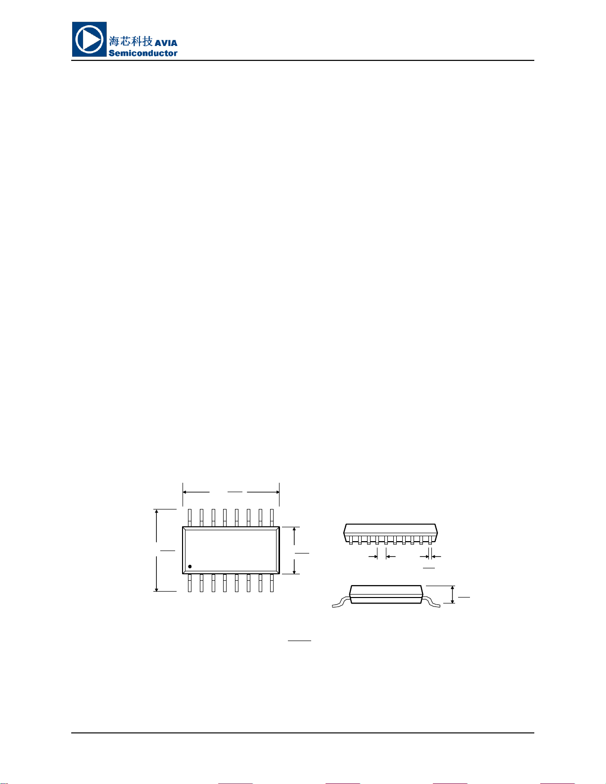
SOP-16L Package
Unit: mm
MAX
MIN
Typ
6.00
9.90
4.10
3.70
3.90
Reference Driver(C)
//-------------------------------------------------------------------
sbit ADDO = P1^5;
sbit ADSK = P0^0;
unsigned long ReadCount(void){
unsigned long Count;
unsigned char i;
ADDO=1;
ADSK=0;
Count=0;
while(ADDO);
for (i=0;i<24;i++){
ADSK=1;
Count=Count<<1;
ADSK=0;
if(ADDO) Count++;
}
ADSK=1;
Count=Count^0x800000;
ADSK=0;
return(Count);
}
Package Dimensions
AVIA SEMICONDUCTOR V2.0
Page 9
9
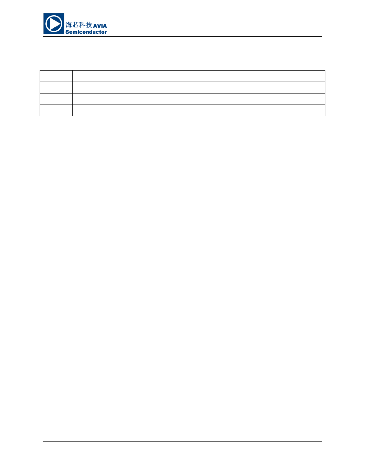
revision
record
1.0
initial version
2.0
change “Reset and Power-Down”
Revision History
HX711
AVIA SEMICONDUCTOR V2.0
 Loading...