


SiFive FE310-G002 Manual
v19p05
© SiFive, Inc.

SiFive FE310-G002 Manual
Proprietary Notice
Copyright © 2019, SiFive Inc. All rights reserved.
Information in this document is provided “as is,” with all faults.
SiFive expressly disclaims all warranties, representations, and conditions of any kind, whether
express or implied, including, but not limited to, the implied warranties or conditions of merchantability, fitness for a particular purpose and non-infringement.
SiFive does not assume any liability rising out of the application or use of any product or circuit,
and specifically disclaims any and all liability, including without limitation indirect, incidental, special, exemplary, or consequential damages.
SiFive reserves the right to make changes without further notice to any products herein.
Release Information
Version Date Changes
v19p04 April 11, 2019 • Initial release
v19p05 May 08, 2019 • Correct UART1 pin assignment

Contents
1 Introduction ..............................................................................................................8
1.1 FE310-G002 Overview ................................................................................................8
1.2 E31 RISC‑V Core .....................................................................................................10
1.3 Interrupts .................................................................................................................10
1.4 On-Chip Memory System...........................................................................................11
1.5 Always-On (AON) Block ............................................................................................11
1.6 GPIO Complex ......................................................................................................... 11
1.7 Universal Asynchronous Receiver/Transmitter.............................................................11
1.8 Hardware Serial Peripheral Interface (SPI) ..................................................................11
1.9 Pulse Width Modulation.............................................................................................12
1.10 I²C .........................................................................................................................12
1.11 Debug Support .......................................................................................................12
2 List of Abbreviations and Terms .................................................................13
3 E31 RISC-V Core ..................................................................................................15
3.1 Instruction Memory System........................................................................................15
3.1.1 I-Cache Reconfigurability ..................................................................................16
3.2 Instruction Fetch Unit ................................................................................................16
3.3 Execution Pipeline ....................................................................................................16
3.4 Data Memory System................................................................................................17
3.5 Atomic Memory Operations........................................................................................17
3.6 Supported Modes .....................................................................................................18
3.7 Physical Memory Protection (PMP).............................................................................18
3.7.1 Functional Description ......................................................................................18
3.7.2 Region Locking ................................................................................................18
3.8 Hardware Performance Monitor..................................................................................19
4 Memory Map ...........................................................................................................21
1

5 Boot Process.......................................................................................................... 23
5.1 Reset Vector............................................................................................................. 23
5.1.1 Mask ROM (MROM).........................................................................................24
5.1.2 One-Time Programmable (OTP) Memory ...........................................................24
5.1.3 Quad SPI Flash Controller (QSPI)......................................................................24
6 Clock Generation .................................................................................................25
6.1 Clock Generation Overview .......................................................................................25
6.2 PRCI Address Space Usage ......................................................................................26
6.3 Internal Trimmable Programmable 72 MHz Oscillator (HFROSC) ..................................26
6.4 External 16 MHz Crystal Oscillator (HFXOSC).............................................................27
6.5 Internal High-Frequency PLL (HFPLL) ........................................................................28
6.6 PLL Output Divider.................................................................................................... 30
6.7 Internal Programmable Low-Frequency Ring Oscillator (LFROSC) ................................31
2
6.8 Alternate Low-Frequency Clock (LFALTCLK)...............................................................32
6.9 Clock Summary ........................................................................................................ 32
7 Power Modes.......................................................................................................... 33
7.1 Run Mode ................................................................................................................33
7.2 Wait Mode................................................................................................................ 33
7.3 Sleep Mode..............................................................................................................33
8 Interrupts..................................................................................................................35
8.1 Interrupt Concepts ....................................................................................................35
8.2 Interrupt Operation....................................................................................................36
8.2.1 Interrupt Entry and Exit .....................................................................................36
8.3 Interrupt Control Status Registers...............................................................................37
8.3.1 Machine Status Register (mstatus) ..................................................................37
8.3.2 Machine Trap Vector (mtvec)............................................................................37
8.3.3 Machine Interrupt Enable (mie) .........................................................................39
8.3.4 Machine Interrupt Pending (mip) .......................................................................39
8.3.5 Machine Cause (mcause) .................................................................................39
8.4 Interrupt Priorities .....................................................................................................40

8.5 Interrupt Latency.......................................................................................................41
9 Core-Local Interruptor (CLINT).....................................................................42
9.1 CLINT Memory Map..................................................................................................42
9.2 MSIP Registers.........................................................................................................42
9.3 Timer Registers ........................................................................................................ 43
10 Platform-Level Interrupt Controller (PLIC)...........................................44
10.1 Memory Map ..........................................................................................................44
10.2 Interrupt Sources ....................................................................................................45
10.3 Interrupt Priorities.................................................................................................... 46
10.4 Interrupt Pending Bits ..............................................................................................46
10.5 Interrupt Enables.....................................................................................................47
10.6 Priority Thresholds .................................................................................................. 48
3
10.7 Interrupt Claim Process ........................................................................................... 48
10.8 Interrupt Completion................................................................................................49
11 Error Device .........................................................................................................51
12 One-Time Programmable Memory (OTP) Peripheral......................52
12.1 Memory Map ..........................................................................................................52
12.2 Programmed-I/O lock register (otp_lock)................................................................53
12.3 Programmed-I/O Sequencing...................................................................................54
12.4 Read sequencer control register (otp_rsctrl) ........................................................54
12.5 OTP Programming Warnings....................................................................................54
12.6 OTP Programming Procedure ..................................................................................55
13 Always-On (AON) Domain ............................................................................56
13.1 AON Power Source.................................................................................................57
13.2 AON Clocking.........................................................................................................57
13.3 AON Reset Unit ...................................................................................................... 57
13.4 Power-On Reset Circuit ...........................................................................................57
13.5 External Reset Circuit..............................................................................................58
13.6 Reset Cause...........................................................................................................58

13.7 Watchdog Timer (WDT) ........................................................................................... 58
13.8 Real-Time Clock (RTC)............................................................................................58
13.9 Backup Registers....................................................................................................58
13.10 Power-Management Unit (PMU) .............................................................................58
13.11 AON Memory Map.................................................................................................58
14 Watchdog Timer (WDT) ..................................................................................61
14.1 Watchdog Count Register (wdogcount) ...................................................................61
14.2 Watchdog Clock Selection ....................................................................................... 62
14.3 Watchdog Configuration Register (wdogcfg).............................................................62
14.4 Watchdog Compare Register (wdogcmp)...................................................................63
14.5 Watchdog Key Register (wdogkey) ..........................................................................63
14.6 Watchdog Feed Address (wdogfeed).......................................................................64
14.7 Watchdog Configuration ..........................................................................................64
4
14.8 Watchdog Resets.................................................................................................... 64
14.9 Watchdog Interrupts (wdogip0) ...............................................................................64
15 Power-Management Unit (PMU).................................................................65
15.1 PMU Overview........................................................................................................ 66
15.2 Memory Map ..........................................................................................................66
15.3 PMU Key Register (pmukey)....................................................................................67
15.4 PMU Program.........................................................................................................67
15.5 Initiate Sleep Sequence Register (pmusleep) ...........................................................68
15.6 Wakeup Signal Conditioning ....................................................................................68
15.7 PMU Interrupt Enables (pmuie) and Wakeup Cause (pmucause) ...............................69
16 Real-Time Clock (RTC) ...................................................................................71
16.1 RTC Count Registers (rtccounthi/rtccountlo) ...................................................71
16.2 RTC Configuration Register (rtccfg) ......................................................................72
16.3 RTC Compare Register (rtccmp) ............................................................................72
17 General Purpose Input/Output Controller (GPIO) ............................74
17.1 GPIO Instance in FE310-G002.................................................................................76

17.2 Memory Map ..........................................................................................................76
17.3 Input / Output Values ............................................................................................... 76
17.4 Interrupts................................................................................................................ 77
17.5 Internal Pull-Ups ..................................................................................................... 77
17.6 Drive Strength.........................................................................................................77
17.7 Output Inversion .....................................................................................................77
17.8 HW I/O Functions (IOF) ...........................................................................................77
18 Universal Asynchronous Receiver/Transmitter (UART)...............79
18.1 UART Overview ...................................................................................................... 79
18.2 UART Instances in FE310-G002...............................................................................79
18.3 Memory Map ..........................................................................................................80
18.4 Transmit Data Register (txdata) .............................................................................80
18.5 Receive Data Register (rxdata)..............................................................................80
5
18.6 Transmit Control Register (txctrl) .........................................................................81
18.7 Receive Control Register (rxctrl) ..........................................................................81
18.8 Interrupt Registers (ip and ie) ................................................................................82
18.9 Baud Rate Divisor Register (div) .............................................................................82
19 Serial Peripheral Interface (SPI) ................................................................84
19.1 SPI Overview.......................................................................................................... 84
19.2 SPI Instances in FE310-G002 ..................................................................................84
19.3 Memory Map ..........................................................................................................85
19.4 Serial Clock Divisor Register (sckdiv) .....................................................................86
19.5 Serial Clock Mode Register (sckmode) .....................................................................87
19.6 Chip Select ID Register (csid) ................................................................................87
19.7 Chip Select Default Register (csdef) .......................................................................88
19.8 Chip Select Mode Register (csmode)........................................................................88
19.9 Delay Control Registers (delay0 and delay1) .........................................................89
19.10 Frame Format Register (fmt).................................................................................89
19.11 Transmit Data Register (txdata) ...........................................................................90
19.12 Receive Data Register (rxdata) ............................................................................91
19.13 Transmit Watermark Register (txmark) ..................................................................91

19.14 Receive Watermark Register (rxmark) ...................................................................92
19.15 SPI Interrupt Registers (ie and ip) ........................................................................92
19.16 SPI Flash Interface Control Register (fctrl) ..........................................................93
19.17 SPI Flash Instruction Format Register (ffmt) ..........................................................93
20 Pulse Width Modulator (PWM) ...................................................................94
20.1 PWM Overview .......................................................................................................94
20.2 PWM Instances in FE310-G002 ...............................................................................95
20.3 PWM Memory Map .................................................................................................95
20.4 PWM Count Register (pwmcount) ............................................................................96
20.5 PWM Configuration Register (pwmcfg) .....................................................................97
20.6 Scaled PWM Count Register (pwms).........................................................................98
20.7 PWM Compare Registers (pwmcmp0–pwmcmp3) ........................................................98
20.8 Deglitch and Sticky Circuitry.....................................................................................99
6
20.9 Generating Left- or Right-Aligned PWM Waveforms .................................................100
20.10 Generating Center-Aligned (Phase-Correct) PWM Waveforms ................................100
20.11 Generating Arbitrary PWM Waveforms using Ganging............................................101
20.12 Generating One-Shot Waveforms .........................................................................102
20.13 PWM Interrupts...................................................................................................102
21 Inter-Integrated Circuit (I²C) Master Interface ..................................103
21.1 I²C Instance in FE310-G002...................................................................................103
22 Debug .................................................................................................................... 104
22.1 Debug CSRs ........................................................................................................104
22.1.1 Trace and Debug Register Select (tselect)..................................................104
22.1.2 Trace and Debug Data Registers (tdata1-3) ................................................105
22.1.3 Debug Control and Status Register (dcsr) .....................................................106
22.1.4 Debug PC dpc ............................................................................................. 106
22.1.5 Debug Scratch dscratch.............................................................................106
22.2 Breakpoints ..........................................................................................................106
22.2.1 Breakpoint Match Control Register mcontrol ................................................106
22.2.2 Breakpoint Match Address Register (maddress).............................................108

22.2.3 Breakpoint Execution ....................................................................................108
22.2.4 Sharing Breakpoints Between Debug and Machine Mode ................................109
22.3 Debug Memory Map..............................................................................................109
22.3.1 Debug RAM and Program Buffer (0x300–0x3FF) ...........................................109
22.3.2 Debug ROM (0x800–0xFFF) ........................................................................109
22.3.3 Debug Flags (0x100–0x110, 0x400–0x7FF) ................................................110
22.3.4 Safe Zero Address........................................................................................110
23 Debug Interface................................................................................................111
23.1 JTAG TAPC State Machine ....................................................................................111
23.2 Resetting JTAG Logic............................................................................................112
23.3 JTAG Clocking......................................................................................................112
23.4 JTAG Standard Instructions ...................................................................................113
23.5 JTAG Debug Commands .......................................................................................113
7
24 References..........................................................................................................114

Chapter 1
Introduction
The FE310-G002 is the second revision of the General Purpose Freedom E300 family.
The FE310-G002 is built around the E31 Core Complex instantiated in the Freedom E300 platform and fabricated in the TSMC CL018G 180nm process. This manual serves as an architectural reference and integration guide for the FE310-G002.
The FE310-G002 is compatible with all applicable RISC‑V standards, and this document should
be read together with the official RISC‑V user-level, privileged, and external debug architecture
specifications.
1.1 FE310-G002 Overview
Figure 1 shows the overall block diagram of the FE310-G002.
A feature summary table can be found in Table 1.
8

Copyright © 2019, SiFive Inc. All rights reserved. 9
Figure 1: FE310-G002 top-level block diagram.

Copyright © 2019, SiFive Inc. All rights reserved. 10
Feature Description
1× E31 RISC‑V cores with machine and user mode,
RISC-V Core
Interrupts
UART 0
UART 1
QSPI 0
SPI 1 Serial Peripheral Interface. SPI 1 has 4 chip select signals.
SPI 2 Serial Peripheral Interface. SPI 2 has 1 chip select signal.
PWM 0 8-bit Pulse-width modulator with 4 comparators.
PWM 1 16-bit Pulse-width modulator with 4 comparators.
PWM 2 16-bit Pulse-width modulator with 4 comparators.
I²C 0 Inter-Integrated Circuit (I²C) controller.
GPIO 32 General Purpose I/O pins.
Always On
Domain
16 KiB 2-way L1 I-cache, and 16 KiB data tightly integrated memory (DTIM).
Software and timer interrupts, 52 peripheral interrupts connected to the PLIC with 7 levels of priority.
Universal Asynchronous/Synchronous Transmitters for
serial communication.
Universal Asynchronous/Synchronous Transmitters for
serial communication.
Serial Peripheral Interface. QSPI 0 has 1 chip select signal.
Supports low-power operation and wakeup.
Table 1: FE310-G002 Feature Summary.
Available in
QFN48
✔
✔
✔
✔
✔
(4 DQ lines)
✔
(3 CS lines)
(2 DQ lines)
✔
✔
✔
✔
✔
✔
1.2 E31 RISC‑V Core
The FE310-G002 includes a 32-bit E31 RISC‑V core, which has a high-performance singleissue in-order execution pipeline, with a peak sustainable execution rate of one instruction per
clock cycle. The E31 core supports Machine and User privilege modes as well as standard Multiply, Atomic, and Compressed RISC‑V extensions (RV32IMAC).
The core is described in more detail in Chapter 3.
1.3 Interrupts
The FE310-G002 includes a RISC-V standard platform-level interrupt controller (PLIC), which
supports 52 global interrupts with 7 priority levels. The FE310-G002 also provides the standard
RISC‑V machine-mode timer and software interrupts via the Core-Local Interruptor (CLINT).
Interrupts are described in Chapter 8. The CLINT is described in Chapter 9. The PLIC is
described in Chapter 10.

Copyright © 2019, SiFive Inc. All rights reserved. 11
1.4 On-Chip Memory System
The E31 core has a(n) 2-way set-associative 16 KiB L1 instruction cache and a(n) 16 KiB L1
DTIM.
All cores have Physical Memory Protection (PMP) units.
The Level 1 memories are described in Chapter 3. The PMP is described in Section 3.7.
1.5 Always-On (AON) Block
The AON block contains the reset logic for the chip, an on-chip low-frequency oscillator, a
watchdog timer, connections for an off-chip low-frequency oscillator, the real-time clock, a programmable power-management unit, and 32×32-bit backup registers that retain state while the
rest of the chip is in a low-power mode.
The AON can be instructed to put the system to sleep. The AON can be programmed to exit
sleep mode on a real-time clock interrupt or when the external digital wakeup pin, dwakeup_n, is
pulled low. The dwakeup_n input supports wired-OR connections of multiple wakeup sources.
The Always-On block is described in Chapter 13.
1.6 GPIO Complex
The GPIO complex manages the connection of digital I/O pads to digital peripherals, including
SPI, UART, I²C, and PWM controllers, as well as for regular programmed I/O operations.
The GPIO complex is described in more detail in Chapter 17.
1.7 Universal Asynchronous Receiver/Transmitter
Multiple universal asynchronous receiver/transmitter (UARTs) are available and provide a
means for serial communication between the FE310-G002 and off-chip devices.
The UART peripherals are described in Chapter 18.
1.8 Hardware Serial Peripheral Interface (SPI)
There are 3 serial peripheral interface (SPI) controllers. Each controller provides a means for
serial communication between the FE310-G002 and off-chip devices, like quad-SPI Flash memory. Each controller supports master-only operation over single-lane, dual-lane, and quad-lane
protocols. Each controller supports burst reads of 32 bytes over TileLink to accelerate instruction cache refills. 1 SPI controller can be programmed to support eXecute-In-Place (XIP) modes
to reduce SPI command overhead on instruction cache refills.

Copyright © 2019, SiFive Inc. All rights reserved. 12
The SPI interface is described in more detail in Chapter 19.
1.9 Pulse Width Modulation
The pulse width modulation (PWM) peripheral can generate multiple types of waveforms on
GPIO output pins and can also be used to generate several forms of internal timer interrupt.
The PWM peripherals are described in Chapter 20.
1.10 I²C
The FE310-G002 has an I²C controller to communicate with external I²C devices, such as sensors, ADCs, etc.
The I²C is described in detail in Chapter 21.
1.11 Debug Support
The FE310-G002 provides external debugger support over an industry-standard JTAG port,
including 8 hardware-programmable breakpoints per hart.
Debug support is described in detail in Chapter 22, and the debug interface is described in
Chapter 23.

Chapter 2
List of Abbreviations and Terms
13

Copyright © 2019, SiFive Inc. All rights reserved. 14
Term Definition
BHT Branch History Table
BTB Branch Target Buffer
RAS Return-Address Stack
CLINT Core-Local Interruptor. Generates per-hart software interrupts and timer
interrupts.
CLIC Core-Local Interrupt Controller. Configures priorities and levels for core
local interrupts.
hart HARdware Thread
DTIM Data Tightly Integrated Memory
ITIM Instruction Tightly Integrated Memory
JTAG Joint Test Action Group
LIM Loosely Integrated Memory. Used to describe memory space delivered in
a SiFive Core Complex but not tightly integrated to a CPU core.
PMP Physical Memory Protection
PLIC Platform-Level Interrupt Controller. The global interrupt controller in a
RISC-V system.
TileLink A free and open interconnect standard originally developed at UC Berke-
ley.
RO Used to describe a Read Only register field.
RW Used to describe a Read/Write register field.
WO Used to describe a Write Only registers field.
WARL Write-Any Read-Legal field. A register field that can be written with any
value, but returns only supported values when read.
WIRI Writes-Ignored, Reads-Ignore field. A read-only register field reserved for
future use. Writes to the field are ignored, and reads should ignore the
value returned.
WLRL Write-Legal, Read-Legal field. A register field that should only be written
with legal values and that only returns legal value if last written with a
legal value.
WPRI Writes-Preserve Reads-Ignore field. A register field that might contain
unknown information. Reads should ignore the value returned, but writes
to the whole register should preserve the original value.

Chapter 3
E31 RISC-V Core
This chapter describes the 32-bit E31 RISC‑V processor core used in the FE310-G002. The
E31 processor core comprises an instruction memory system, an instruction fetch unit, an execution pipeline, a data memory system, and support for global, software, and timer interrupts.
The E31 feature set is summarized in Table 2.
Feature Description
ISA RV32IMAC.
Instruction Cache 16 KiB 2-way instruction cache.
Instruction Tightly Integrated Memory The E31 has support for an ITIM with a maxi-
mum size of 8 KiB.
Data Tightly Integrated Memory 16 KiB DTIM.
Modes The E31 supports the following modes:
Machine Mode, User Mode.
Table 2: E31 Feature Set
3.1 Instruction Memory System
The instruction memory system consists of a dedicated 16 KiB 2-way set-associative instruction
cache. The access latency of all blocks in the instruction memory system is one clock cycle. The
instruction cache is not kept coherent with the rest of the platform memory system. Writes to
instruction memory must be synchronized with the instruction fetch stream by executing a
FENCE.I instruction.
The instruction cache has a line size of 32 bytes, and a cache line fill triggers a burst access.
The core caches instructions from executable addresses, with the exception of the Instruction
Tightly Integrated Memory (ITIM), which is further described in Section 3.1.1. See the
FE310-G002 Memory Map in Chapter 4 for a description of executable address regions that are
denoted by the attribute X.
Trying to execute an instruction from a non-executable address results in a synchronous trap.
15

Copyright © 2019, SiFive Inc. All rights reserved. 16
3.1.1 I-Cache Reconfigurability
The instruction cache can be partially reconfigured into ITIM, which occupies a fixed address
range in the memory map. ITIM provides high-performance, predictable instruction delivery.
Fetching an instruction from ITIM is as fast as an instruction-cache hit, with no possibility of a
cache miss. ITIM can hold data as well as instructions, though loads and stores from a core to
its ITIM are not as performant as loads and stores to its Data Tightly Integrated Memory (DTIM).
The instruction cache can be configured as ITIM for all ways except for 1 in units of cache lines
(32 bytes). A single instruction cache way must remain an instruction cache. ITIM is allocated
simply by storing to it. A store to the nthbyte of the ITIM memory map reallocates the first n+1
bytes of instruction cache as ITIM, rounded up to the next cache line.
ITIM is deallocated by storing zero to the first byte after the ITIM region, that is, 8 KiB after the
base address of ITIM as indicated in the Memory Map in Chapter 4. The deallocated ITIM space
is automatically returned to the instruction cache.
For determinism, software must clear the contents of ITIM after allocating it. It is unpredictable
whether ITIM contents are preserved between deallocation and allocation.
3.2 Instruction Fetch Unit
The E31 instruction fetch unit contains branch prediction hardware to improve performance of
the processor core. The branch predictor comprises a 28-entry branch target buffer (BTB) which
predicts the target of taken branches, a 512-entry branch history table (BHT), which predicts the
direction of conditional branches, and a 6-entry return-address stack (RAS) which predicts the
target of procedure returns. The branch predictor has a one-cycle latency, so that correctly predicted control-flow instructions result in no penalty. Mispredicted control-flow instructions incur a
three-cycle penalty.
The E31 implements the standard Compressed (C) extension to the RISC‑V architecture, which
allows for 16-bit RISC‑V instructions.
3.3 Execution Pipeline
The E31 execution unit is a single-issue, in-order pipeline. The pipeline comprises five stages:
instruction fetch, instruction decode and register fetch, execute, data memory access, and register writeback.
The pipeline has a peak execution rate of one instruction per clock cycle, and is fully bypassed
so that most instructions have a one-cycle result latency. There are several exceptions:
• LW has a two-cycle result latency, assuming a cache hit.
• LH, LHU, LB, and LBU have a three-cycle result latency, assuming a cache hit.
• CSR reads have a three-cycle result latency.

Copyright © 2019, SiFive Inc. All rights reserved. 17
• MUL, MULH, MULHU, and MULHSU have a 5-cycle result latency.
• DIV, DIVU, REM, and REMU have between a 2-cycle and 33-cycle result latency, depending
on the operand values.
The pipeline only interlocks on read-after-write and write-after-write hazards, so instructions
may be scheduled to avoid stalls.
The E31 implements the standard Multiply (M) extension to the RISC‑V architecture for integer
multiplication and division. The E31 has a 8-bit per cycle hardware multiply and a 1-bit per cycle
hardware divide. The multiplier can only execute one operation at a time and will block until the
previous operation completes.
The hart will not abandon a Divide instruction in flight. This means if an interrupt handler tries to
use a register that is the destination register of a divide instruction the pipeline stalls until the
divide is complete.
Branch and jump instructions transfer control from the memory access pipeline stage. Correctlypredicted branches and jumps incur no penalty, whereas mispredicted branches and jumps
incur a three-cycle penalty.
Most CSR writes result in a pipeline flush with a five-cycle penalty.
3.4 Data Memory System
The E31 data memory system consists of a DTIM. The access latency from a core to its own
DTIM is two clock cycles for full words and three clock cycles for smaller quantities. Misaligned
accesses are not supported in hardware and result in a trap to allow software emulation.
Stores are pipelined and commit on cycles where the data memory system is otherwise idle.
Loads to addresses currently in the store pipeline result in a five-cycle penalty.
3.5 Atomic Memory Operations
The E31 core supports the RISC‑V standard Atomic (A) extension on the DTIM and the peripheral memory region. Atomic memory operations to regions that do not support them generate an
access exception precisely at the core.
The load-reserved and store-conditional instructions are only supported on cached regions,
hence generate an access exception on DTIM and other uncached memory regions.
See The RISC‑V Instruction Set Manual, Volume I: User-Level ISA, Version 2.1 for more infor-
mation on the instructions added by this extension.

Copyright © 2019, SiFive Inc. All rights reserved. 18
3.6 Supported Modes
The E31 supports RISC‑V user mode, providing two levels of privilege: machine (M) and user
(U). U-mode provides a mechanism to isolate application processes from each other and from
trusted code running in M-mode.
See The RISC‑V Instruction Set Manual, Volume II: Privileged Architecture, Version 1.10 for
more information on the privilege modes.
3.7 Physical Memory Protection (PMP)
The E31 includes a Physical Memory Protection (PMP) unit compliant with The RISC‑V Instruction Set Manual, Volume II: Privileged Architecture, Version 1.10. PMP can be used to set mem-
ory access privileges (read, write, execute) for specified memory regions. The E31 PMP supports 8 regions with a minimum region size of 4 bytes.
This section describes how PMP concepts in the RISC‑V architecture apply to the E31. The
definitive resource for information about the RISC‑V PMP is The RISC‑V Instruction Set Manual,
Volume II: Privileged Architecture, Version 1.10.
3.7.1 Functional Description
The E31 includes a PMP unit, which can be used to restrict access to memory and isolate
processes from each other.
The E31 PMP unit has 8 regions and a minimum granularity of 4 bytes. Overlapping regions are
permitted. The E31 PMP unit implements the architecturally defined pmpcfgX CSRs pmpcfg0
and pmpcfg1 supporting 8 regions. pmpcfg2 and pmpcfg3 are implemented but hardwired to
zero.
The PMP registers may only be programmed in M-mode. Ordinarily, the PMP unit enforces permissions on U-mode accesses. However, locked regions (see Section 3.7.2) additionally
enforce their permissions on M-mode.
3.7.2 Region Locking
The PMP allows for region locking whereby, once a region is locked, further writes to the configuration and address registers are ignored. Locked PMP entries may only be unlocked with a
system reset. A region may be locked by setting the L bit in the pmpicfg register.
In addition to locking the PMP entry, the L bit indicates whether the R/W/X permissions are
enforced on M-Mode accesses. When the L bit is clear, the R/W/X permissions apply only to Umode.

Copyright © 2019, SiFive Inc. All rights reserved. 19
3.8 Hardware Performance Monitor
The FE310-G002 supports a basic hardware performance monitoring facility compliant with The
RISC‑V Instruction Set Manual, Volume II: Privileged Architecture, Version 1.10. The mcycle
CSR holds a count of the number of clock cycles the hart has executed since some arbitrary
time in the past. The minstret CSR holds a count of the number of instructions the hart has
retired since some arbitrary time in the past. Both are 64-bit counters. The mcycle and
minstret CSRs hold the 32 least-significant bits of the corresponding counter, and the mcycleh
and minstreth CSRs hold the most-significant 32 bits.
The hardware performance monitor includes two additional event counters, mhpmcounter3 and
mhpmcounter4. The event selector CSRs mhpmevent3 and mhpmevent4 are registers that con-
trol which event causes the corresponding counter to increment. The mhpmcounters are 40-bit
counters. The mhpmcounter_i CSR holds the 32 least-significant bits of the corresponding
counter, and the mhpmcounter_ih CSR holds the 8 most-significant bits.
The event selectors are partitioned into two fields, as shown in Table 3: the lower 8 bits select
an event class, and the upper bits form a mask of events in that class. The counter increments if
the event corresponding to any set mask bit occurs. For example, if mhpmevent3 is set to
0x4200, then mhpmcounter3 will increment when either a load instruction or a conditional
branch instruction retires. An event selector of 0 means "count nothing."
Note that in-flight and recently retired instructions may or may not be reflected when reading or
writing the performance counters or writing the event selectors.

Copyright © 2019, SiFive Inc. All rights reserved. 20
Machine Hardware Performance Monitor Event Register
Instruction Commit Events, mhpeventX[7:0] = 0
Bits Meaning
8 Exception taken
9 Integer load instruction retired
10 Integer store instruction retired
11 Atomic memory operation retired
12 System instruction retired
13 Integer arithmetic instruction retired
14 Conditional branch retired
15 JAL instruction retired
16 JALR instruction retired
17 Integer multiplication instruction retired
18 Integer division instruction retired
Microarchitectural Events , mhpeventX[7:0] = 1
Bits Meaning
8 Load-use interlock
9 Long-latency interlock
10 CSR read interlock
11 Instruction cache/ITIM busy
12 Data cache/DTIM busy
13 Branch direction misprediction
14 Branch/jump target misprediction
15 Pipeline flush from CSR write
16 Pipeline flush from other event
17 Integer multiplication interlock
Memory System Events, mhpeventX[7:0] = 2
Bits Meaning
8 Instruction cache miss
9 Memory-mapped I/O access
Table 3: mhpmevent Register Description

Chapter 4
Memory Map
The memory map of the FE310-G002 is shown in Table 4.
21

Copyright © 2019, SiFive Inc. All rights reserved. 22
Base Top Attr. Description Notes
0x0000_0000 0x0000_0FFF RWX A Debug
0x0000_1000 0x0000_1FFF R XC Mode Select
0x0000_2000 0x0000_2FFF Reserved
0x0000_3000 0x0000_3FFF RWX A Error Device
0x0000_4000 0x0000_FFFF Reserved
0x0001_0000 0x0001_1FFF R XC Mask ROM (8 KiB)
0x0001_2000 0x0001_FFFF Reserved
0x0002_0000 0x0002_1FFF R XC OTP Memory Region
0x0002_2000 0x001F_FFFF Reserved
0x0200_0000 0x0200_FFFF RW A CLINT
0x0201_0000 0x07FF_FFFF Reserved
0x0800_0000 0x0800_1FFF RWX A E31 ITIM (8 KiB)
0x0800_2000 0x0BFF_FFFF Reserved
0x0C00_0000 0x0FFF_FFFF RW A PLIC
0x1000_0000 0x1000_0FFF RW A AON
0x1000_1000 0x1000_7FFF Reserved
0x1000_8000 0x1000_8FFF RW A PRCI
0x1000_9000 0x1000_FFFF Reserved
0x1001_0000 0x1001_0FFF RW A OTP Control
0x1001_1000 0x1001_1FFF Reserved
0x1001_2000 0x1001_2FFF RW A GPIO
0x1001_3000 0x1001_3FFF RW A UART 0
0x1001_4000 0x1001_4FFF RW A QSPI 0
0x1001_5000 0x1001_5FFF RW A PWM 0
0x1001_6000 0x1001_6FFF RW A I2C 0
0x1001_7000 0x1002_2FFF Reserved
0x1002_3000 0x1002_3FFF RW A UART 1
0x1002_4000 0x1002_4FFF RW A SPI 1
0x1002_5000 0x1002_5FFF RW A PWM 1
0x1002_6000 0x1003_3FFF Reserved
0x1003_4000 0x1003_4FFF RW A SPI 2
0x1003_5000 0x1003_5FFF RW A PWM 2
0x1003_6000 0x1FFF_FFFF Reserved
0x2000_0000 0x3FFF_FFFF R XC QSPI 0 Flash
(512 MiB)
0x4000_0000 0x7FFF_FFFF Reserved
0x8000_0000 0x8000_3FFF RWX A E31 DTIM (16 KiB)
0x8000_4000 0xFFFF_FFFF Reserved
Debug Address Space
On-Chip Non Volatile Memory
On-Chip Peripherals
Off-Chip Non-Volatile Memory
On-Chip Volatile Memory
Table 4: FE310-G002 Memory Map. Memory Attributes: R - Read, W - Write, X - Execute, C -
Cacheable, A - Atomics

Chapter 5
Boot Process
The FE310-G002 supports booting from several sources, which are controlled using the Mode
Select (MSEL[1:0]) pins on the chip. All possible values are enumerated in Table 5.
MSEL Purpose
00 loops forever waiting for debugger
01 jump directly to 0x2000_0000 (memory-mapped QSPI0)
10 jump directly to 0x0002_0000 (OTP)
11 jump directly to 0x0001_0000 (Mask ROM: Default Boot Mode)
Table 5: Boot media based on MSEL pins
5.1 Reset Vector
On power-on, the core’s reset vector is 0x1004.
Address Contents
0x1000 The MSEL pin state
0x1004 auipc t0, 0
0x1008 lw t1, -4(t0)
0x100C slli t1, t1, 0x3
0x1010 add t0, t0, t1
0x1014 lw t0, 252(t0)
0x1018 jr t0
Table 6: Reset vector ROM
This small gate ROM implements an MSEL-dependent jump for all cores as follows:
23

Copyright © 2019, SiFive Inc. All rights reserved. 24
MSEL Reset address Purpose
00 0x0000_1004 loops forever waiting for debugger
01 0x2000_0000 memory-mapped QSPI0
10 0x0002_0000 memory-mapped OTP
11 0x0001_0000 memory-mapped Mask ROM (jumps to OTP)
Table 7: Target of the reset vector
5.1.1 Mask ROM (MROM)
MROM is fixed at design time, and is located on the peripheral bus on FE310-G002, but instructions fetched from MROM are cached by the core’s I-cache. The MROM contains an instruction
at address 0x1_0000 which jumps to the OTP start address at 0x2_0000.
5.1.2 One-Time Programmable (OTP) Memory
The OTP is located on the peripheral bus, with both a control register interface to program the
OTP, and a memory read port interface to fetch words from the OTP. Instruction fetches from the
OTP memory read port are cached in the E31 core’s instruction cache.
The OTP needs to be programmed before use and can only be programmed by code running
on the core. The OTP bits contain all 0s prior to programming.
5.1.3 Quad SPI Flash Controller (QSPI)
The dedicated QSPI flash controller connects to external SPI flash devices that are used for
execute-in-place code. SPI flash is not available in certain scenarios such as package testing or
board designs not using SPI flash (e.g., just using on-chip OTP).
Off-chip SPI devices can vary in number of supported I/O bits (1, 2, or 4). SPI flash bits contain
all 1s prior to programming.

Chapter 6
Clock Generation
The FE310-G002 supports many alternative clock-generation schemes to match application
needs. This chapter describes the structure of the clock generation system. The various clock
configuration registers live either in the AON block (Chapter 13) or the PRCI block (Section 6.2).
6.1 Clock Generation Overview
Figure 2: FE310-G002 clock generation scheme
Figure 2 shows an overview of the FE310-G002 clock generation scheme. Most digital clocks
on the chip are divided down from a central high-frequency clock hfclk produced from either
the PLL or an on-chip trimmable oscillator. The PLL can be driven from either the on-chip oscil-
25

Copyright © 2019, SiFive Inc. All rights reserved. 26
lator or an off-chip crystal oscillator. The off-chip oscillator can also drive the high-frequency
clock directly.
For the FE310-G002, the TileLink bus clock (tlclk) is fixed to be the same as the processor
core clock (coreclk).
The Always-On block includes a real-time clock circuit that is driven from one of the low-frequency clock sources: an off-chip oscillator (LFOSC) or an an on-chip low-frequency oscillator
(LFROSC).
6.2 PRCI Address Space Usage
PRCI (Power, Reset, Clock, Interrupt) is an umbrella term for platform non-AON memorymapped control and status registers controlling component power states, resets, clock selection,
and low-level interrupts, hence the name. The PRCI registers are generally only made visible to
machine-mode software. The AON block contains registers with similar functions, but only for
the AON block units.
Table 8 shows the memory map for the PRCI on the FE310-G002.
Offset Name Description
0x00 hfrosccfg Ring Oscillator Configuration and Status
0x04 hfxosccfg Crystal Oscillator Configuration and Status
0x08 pllcfg PLL Configuration and Status
0x0C plloutdiv PLL Final Divide Configuration
0xF0 procmoncfg Process Monitor Configuration and Status
Table 8: SiFive PRCI memory map, offsets relative to PRCI base address.
6.3 Internal Trimmable Programmable 72 MHz Oscillator (HFROSC)
An internal trimmable high-frequency ring oscillator (HFROSC) is used to provide the default
clock after reset, and can be used to allow operation without an external high-frequency crystal
or the PLL.
The oscillator is controlled by the hfrosccfg register, which is memory-mapped in the PRCI
address space, and whose format is shown in Table 9.

Copyright © 2019, SiFive Inc. All rights reserved. 27
hfrosccfg: Ring Oscillator Configuration and Status (hfrosccfg)
Register Offset 0x0
Bits Field Name Attr. Rst. Description
[5:0] hfroscdiv RW 0x4 Ring Oscillator Divider Register
[15:6] Reserved
[20:16] hfrosctrim RW 0x10 Ring Oscillator Trim Register
[29:21] Reserved
30 hfroscen RW 0x1 Ring Oscillator Enable
31 hfroscrdy RO X Ring Oscillator Ready
Table 9: hfrosccfg: Ring Oscillator Configuration and Status
The frequency can be adjusted in software using a 5-bit trim value in the hfrosctrim. The trim
value (from 0–31) adjusts which tap of the variable delay chain is fed back to the start of the
ring. A value of 0 corresponds to the longest chain and slowest frequency, while higher values
correspond to shorter chains and therefore higher frequencies.
The HFROSC oscillator output frequency can be divided by an integer between 1 and 64 giving
a frequency range of 1.125 MHz–72 MHz assuming the trim value is set to give a 72 MHz output. The value of the divider is given in the hfroscdiv field, where the divide ratio is one greater
than the binary value held in the field (i.e., hfroscdiv=0 indicates divide by 1, hfroscdiv=1
indicates divide by 2, etc.). The value of the divider can be changed at any time.
The HFROSC is the default clock source used for the system core at reset. After a reset, the
hfrosctrim value is reset to 16, the middle of the adjustable range, and the divider is reset to
divide-by-5 (hfroscdiv=4), which gives a nominal 13.8 MHz (±50%) output frequency.
The value of hfrosctrim that most closely achieves an 72 MHz clock output at nominal conditions (1.8 V at 25 °C) is determined by manufacturing-time calibration and is stored in on-chip
OTP storage. Upon reset, software in the processor boot sequence can write the calibrated
value into the hfrosctrim field, but the value can be altered at any time during operation
including when the processor is running from HFROSC.
To save power, the HFROSC can be disabled by clearing hfroscen. The processor must be
running from a different clock source (the PLL, external crystal, or external clock) before disabling HFROSC. HFROSC can be explicitly renabled by setting hfroscen. HFROSC will be
automatically re-enabled at every reset.
The status bit hfroscrdy indicates if the oscillator is operational and ready for use as a clock
source.
6.4 External 16 MHz Crystal Oscillator (HFXOSC)
An external high-frequency 16 MHz crystal oscillator can be used to provide a precise clock
source. The crystal oscillator should have a capacitive load of ≤ 12 pF and an ESR ≤ 80 Ω.

Copyright © 2019, SiFive Inc. All rights reserved. 28
When used to drive the PLL, the 16 MHz crystal oscillator output frequency must be divided by
two in the first-stage divider of the PLL (i.e., ) to provide an 8 MHz reference clock to the
VCO.
The input pad of the HFXOSC can also be used to supply an external clock source, in which
case, the output pad should be left unconnected.
The HFXOSC input can be used to generate hfclk directly if the PLL is set to bypass.
The HFXOSC is controlled via the memory-mapped hfxosccfg register.
hfxosccfg: Crystal Oscillator Configuration and Status (hfxosccfg)
Register Offset 0x4
Bits Field Name Attr. Rst. Description
[29:0] Reserved
30 hfxoscen RW 0x1 Crystal Oscillator Enable
31 hfxoscrdy RO X Crystal Oscillator Ready
Table 10: hfxosccfg: Crystal Oscillator Configuration and Status
The hfxoscen bit turns on the crystal driver and is set on wakeup reset, but can be cleared to
turn off the crystal driver and reduce power consumption. The hfxoscrdy bit indicates if the
crystal oscillator output is ready for use.
The hfxoscen bit must also be turned on to use the HFXOSC input pad to connect an external
clock source.
6.5 Internal High-Frequency PLL (HFPLL)
The PLL generates a high-frequency clock by multiplying a mid-frequency reference source
clock, either the HFROSC or the HFXOSC. The input frequency to the PLL can be in the range
6–48 MHz. The PLL can generate output clock frequencies in the range 48–384 MHz.
The PLL is controlled by a memory-mapped read-write pllcfg register in the PRCI address
space. The format of pllcfg is shown in Table 11.

Copyright © 2019, SiFive Inc. All rights reserved. 29
pllcfg: PLL Configuration and Status (pllcfg)
Register Offset 0x8
Bits Field Name Attr. Rst. Description
[2:0] pllr RW 0x1 PLL R Value
3 Reserved
[9:4] pllf RW 0x1F PLL F Value
[11:10] pllq RW 0x3 PLL Q Value
[15:12] Reserved
16 pllsel RW 0x0 PLL Select
17 pllrefsel RW 0x1 PLL Reference Select
18 pllbypass RW 0x1 PLL Bypass
[30:19] Reserved
31 plllock RO X PLL Lock
Table 11: pllcfg: PLL Configuration and Status
Figure 3 shows how the PLL output frequency is set using a combination of three read-write
fields: pllr[2:0], pllf[2:0], pllq[1:0]. The frequency constraints must be observed
between each stage for correct operation.
Figure 3: Controlling the FE310-G002 PLL output frequency.
The pllr[1:0] field encodes the reference clock divide ratio as a 2-bit binary value, where the
value is one less than the divide ratio (i.e., 00=1, 11=4). The frequency of the output of the reference divider (refr) must lie between 6–12 MHz.
The pllf[5:0] field encodes the PLL VCO multiply ratio as a 6-bit binary value,
divide ratio of
(vco) must lie between 384–768 MHz. Table 12 summarizes the valid settings of the multiply
ratio.
(i.e., 000000=2, 111111=128). The frequency of the VCO output
, signifying a

Copyright © 2019, SiFive Inc. All rights reserved. 30
Legal pllf multiplier vco frequency (MHz)refr (MHz)
Min Max Min Max
6 64 128 384 768
8 48 96 384 768
10 39 76 390 760
12 32 64 384 768
Table 12: Valid PLL multiply ratios. The multiplier setting in the
table is given as the actual multiply ratio; the binary value
stored in pllf field should be
.
The pllq[1:0] field encodes the PLL output divide ratio as follows, 01=2, 10=4, 11=8. The
value 00 is not supported. The final output of the PLL must have a frequency that lies between
48–384 MHz.
The one-bit read-write pllbypass field in the pllcfg register turns off the PLL when written with
a 1 and then pllout is driven directly by the clock indicated by pllrefsel. The other PLL registers can be configured when pllbypass is set. The agent that writes pllcfg should be running from a different clock source before disabling the PLL. The PLL is also disabled with
pllbypass=1 after a wakeup reset.
for a multiply ratio
The pllsel bit must be set to drive the final hfclk with the PLL output, bypassed or otherwise.
When pllsel is clear, the hfroscclk directly drives hfclk. The pllsel bit is clear on wakeup
reset.
The pllcfg register is reset to: bypass and power off the PLL pllbypass=1; input driven from
external HFXOSC oscillator pllrefsel=1; PLL not driving system clock pllsel=0; and the PLL
ratios are set to R=2, F=64, and Q=8 (pllr=01, pllf=011111, pllq=11).
The PLL provides a lock signal which is set when the PLL has achieved lock, and which can be
read from the most-significant bit of the pllcfg register. The PLL requires up to 100 μs to
regain lock once enabled, and the lock signal will not necessarily be stable during this initial lock
period so should only be interrogated after this period. The PLL may not achieve lock and the
lock signal might not remain asserted if there is excessive jitter in the source clock.
The PLL requires dedicated 1.8 V power supply pads with a supply filter on the circuit board.
The supply filter should be a 100 Ω resistor in series with the board 1.8 V supply decoupled with
a 100 nF capacitor across the VDDPLL/VSSPLL supply pins. The VSSPLL pin should not be
connected to board VSS.
6.6 PLL Output Divider
The plloutdiv register controls a clock divider that divides the output of the PLL.
Copyright © 2019, SiFive Inc. All rights reserved. 31
plloutdiv: PLL Final Divide Configuration (plloutdiv)
Register Offset 0xC
Bits Field Name Attr. Rst. Description
[5:0] plloutdiv RW 0x0 PLL Final Divider Value
[7:6] Reserved
[13:8] plloutdivby1 RW 0x1 PLL Final Divide By 1
[31:14] Reserved
Table 13: plloutdiv: PLL Final Divide Configuration
If the plloutdivby1 bit is set, the PLL output clock is passed through undivided. If
plloutdivby1 is clear, the value
(between 2–128). The output divider expands the PLL output frequency range to
0.375–384 MHz.
The plloutdivby1 register is reset to divide-by-1 (plloutdivby1=1).
in plloutdiv sets the clock-divide ratio to
6.7 Internal Programmable Low-Frequency Ring Oscillator (LFROSC)
A second programmable ring oscillator (LFROSC) is used to provide an internal low-frequency
32 kHz clock source. The LFROSC can generate frequencies in the range 1.5–230 kHz
(±45%).
The lfrosccfg register lives in the AON block as shown in Table 36.
At power-on reset, the LFROSC resets to selecting the middle tap (lfrosctrim=16) and ÷5
(lfroscdiv=4), resulting in an output frequency of
The LFROSC can be calibrated in software using a more accurate high-frequency clock source.
lfrosccfg: Ring Oscillator Configuration and Status (lfrosccfg)
Register Offset 0x70
Bits Field Name Attr. Rst. Description
[5:0] lfroscdiv RW 0x4 Ring Oscillator Divider Register
[15:6] Reserved
[20:16] lfrosctrim RW 0x10 Ring Oscillator Trim Register
[29:21] Reserved
30 lfroscen RW 0x1 Ring Oscillator Enable
31 lfroscrdy RO X Ring Oscillator Ready
30 kHz.
Table 14: lfrosccfg: Ring Oscillator Configuration and Status
Copyright © 2019, SiFive Inc. All rights reserved. 32
6.8 Alternate Low-Frequency Clock (LFALTCLK)
An external low-frequency clock can be driven on the psdlfaltclk pad, when the
psdlfaltclksel is tied low. This mux selection can also be controlled by software using the
lfextclk_sel in lfclkmux shown in Table 15. The current value of the psdlfaltclksel pad
can be read in lfextclk_mux_status field.
lfclkmux: Low-Frequency Clock Mux Control and Status (lfclkmux)
Register Offset 0x7C
Bits Field Name Attr. Rst. Description
0 lfextclk_sel RW 0x0 Low Frequency Clock Source Selector
[30:1] Reserved
31 lfextclk_mux_status RO X Setting of the aon_lfclksel pin
Table 15: lfclkmux: Low-Frequency Clock Mux Control and Status
6.9 Clock Summary
Table 16 summarizes the major clocks on the FE310-G002 and their initial reset conditions. At
external reset, the AON domain lfclk is clocked by either the LFROSC or psdlfaltclk, as
selected by psdlfaltclksel. At wakeup reset, the MOFF domain hfclk is clocked by the
HFROSC.
FrequencyName Reset
Source
LFROSC lfroscrst 32 kHz 1.5 kHz 230 kHz ±45%
psdlfaltclk - - 0 kHz 500 kHz When selected
HFROSC hfclkrst 13.8 MHz 0.77 MHz 20 MHz ±45%
HFXOSC crystal hfclkrst ON 10 MHz 20 MHz 16 MHz on
HFXOSC input hfclkrst ON 0 MHz 20 MHz External clock
PLL hfclkrst OFF 0.375 MHz 384 MHz
JTAG TCK - OFF 0 MHz 16 MHz
Table 16: FE310-G002 Clock Sources
Reset Min Max
AON Domain
MOFF Domain
Notes
by
psdlfaltclksel
HiFive
source

Chapter 7
Power Modes
This chapter describes the different power modes available on the FE310-G002. The
FE310-G002 supports three power modes: Run, Wait, and Sleep.
7.1 Run Mode
Run mode corresponds to regular execution where the processor is running. Power consumption can be adjusted by varying the clock frequency of the processor and peripheral bus, and by
enabling or disabling individual peripheral blocks. The processor exits run mode by executing a
"Wait for Interrupt" (WFI) instruction.
7.2 Wait Mode
When the processor executes a WFI instruction it enters Wait mode, which halts instruction execution and gates the clocks driving the processor pipeline. All state is preserved in the system.
The processor will resume in Run mode when there is a local interrupt pending or when the
PLIC sends an interrupt notification. The processor may also exit wait mode for other events,
and software must check system status when exiting wait mode to determine the correct course
of action.
7.3 Sleep Mode
Sleep mode is entered by writing to a memory-mapped register pmusleep in the power-management unit (PMU). The pmusleep register is protected by the pmukey register which must be
written with a defined value before writing to pmusleep.
The PMU will then execute a power-down sequence to turn off power to the processor and main
pads. All volatile state in the system is lost except for state held in the AON domain. The main
output pads will be left floating.
33

Copyright © 2019, SiFive Inc. All rights reserved. 34
Sleep mode is exited when an enabled wakeup event occurs, whereupon the PMU will initiate a
wakeup sequence. The wakeup sequence turns on the core and pad power supplies while
asserting reset on the clocks, core and pads. After the power supplies stabilize, the clock reset
is deasserted to allow the clocks to stabilize. Once the clocks are stable, the pad and processor
resets are deasserted, and the processor begins running from the reset vector.
Software must reinitialize the core and can interrogate the PMU pmucause register to determine
the cause of reset, and can recover pre-sleep state from the backup registers. The processor
always initially runs from the HFROSC at the default setting, and must reconfigure clocks to run
from an alternate clock source (HFXOSC or PLL) or at a different setting on the HFROSC.
Because the FE310-G002 has no internal power regulator, the PMU’s control of the power supplies is through chip outputs, pmu_out_0 and pmu_out_1. The system integrator can use these
outputs to enable and disable the power supplies connected to the FE310-G002.

Chapter 8
Interrupts
This chapter describes how interrupt concepts in the RISC‑V architecture apply to the
FE310-G002.
The definitive resource for information about the RISC‑V interrupt architecture is The RISC‑V
Instruction Set Manual, Volume II: Privileged Architecture, Version 1.10.
8.1 Interrupt Concepts
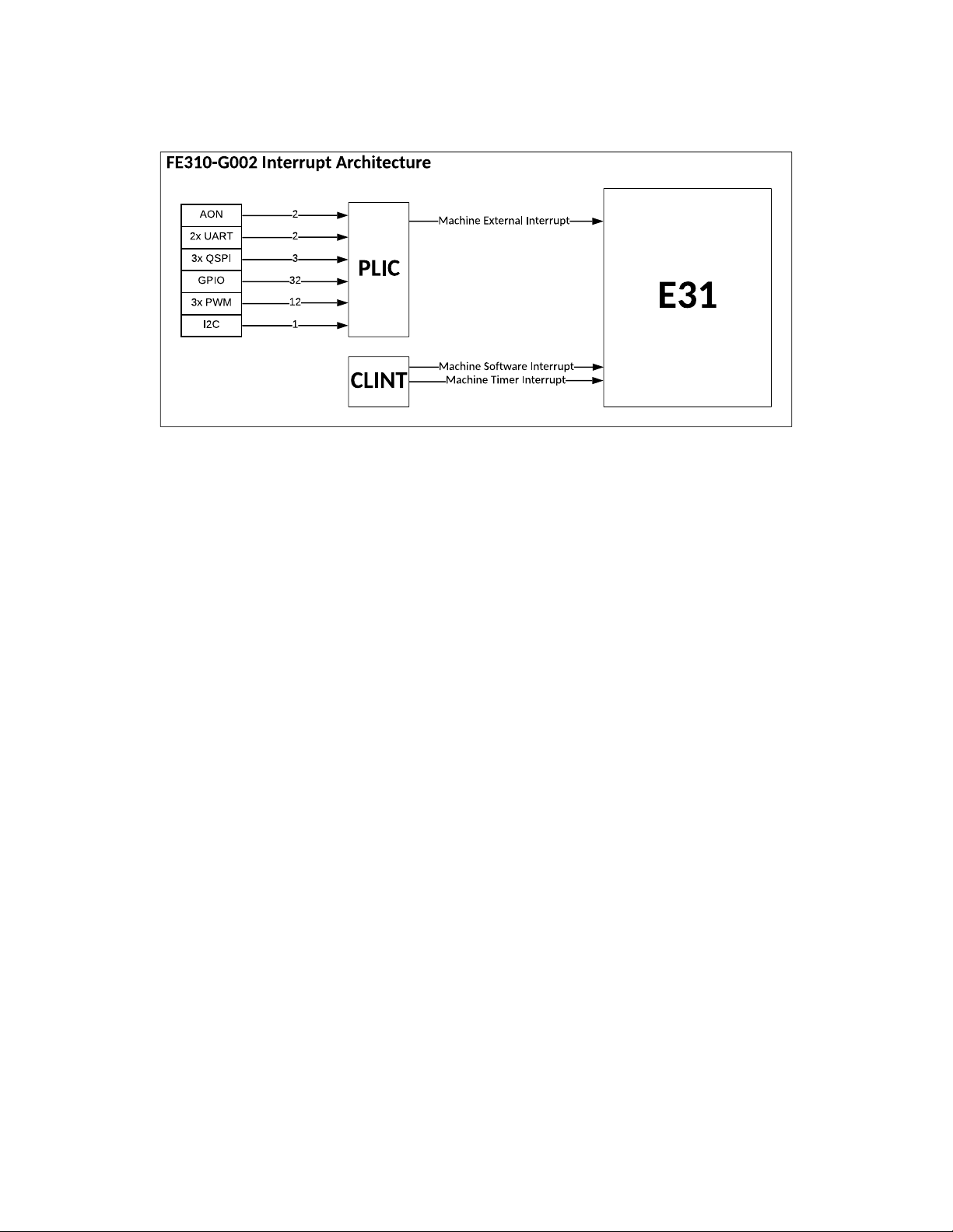
The FE310-G002 supports Machine Mode interrupts. It also has support for the following types
of RISC‑V interrupts: local and global.
Local interrupts are signaled directly to an individual hart with a dedicated interrupt value. This
allows for reduced interrupt latency as no arbitration is required to determine which hart will service a given request and no additional memory accesses are required to determine the cause of
the interrupt.
Software and timer interrupts are local interrupts generated by the Core-Local Interruptor
(CLINT). The FE310-G002 contains no other local interrupt sources.
Global interrupts, by contrast, are routed through a Platform-Level Interrupt Controller (PLIC),
which can direct interrupts to any hart in the system via the external interrupt. Decoupling global
interrupts from the hart(s) allows the design of the PLIC to be tailored to the platform, permitting
a broad range of attributes like the number of interrupts and the prioritization and routing
schemes.
This chapter describes the FE310-G002 interrupt architecture.
Chapter 9 describes the Core-Local Interruptor.
Chapter 10 describes the global interrupt architecture and the PLIC design.
The FE310-G002 interrupt architecture is depicted in Figure 4.
35
Copyright © 2019, SiFive Inc. All rights reserved. 36
Figure 4: FE310-G002 Interrupt Architecture Block Diagram.
8.2 Interrupt Operation
If the global interrupt-enable mstatus.MIE is clear, then no interrupts will be taken. If
mstatus.MIE is set, then pending-enabled interrupts at a higher interrupt level will preempt cur-
rent execution and run the interrupt handler for the higher interrupt level.
When an interrupt or synchronous exception is taken, the privilege mode is modified to reflect
the new privilege mode. The global interrupt-enable bit of the handler’s privilege mode is
cleared.
8.2.1 Interrupt Entry and Exit
When an interrupt occurs:
• The value of mstatus.MIE is copied into mcause.MPIE, and then mstatus.MIE is cleared,
effectively disabling interrupts.
• The privilege mode prior to the interrupt is encoded in mstatus.MPP.
• The current pc is copied into the mepc register, and then pc is set to the value specified by
mtvec as defined by the mtvec.MODE described in Table 19.
At this point, control is handed over to software in the interrupt handler with interrupts disabled.
Interrupts can be re-enabled by explicitly setting mstatus.MIE or by executing an MRET instruction to exit the handler. When an MRET instruction is executed, the following occurs:
• The privilege mode is set to the value encoded in mstatus.MPP.
• The global interrupt enable, mstatus.MIE, is set to the value of mcause.MPIE.
• The pc is set to the value of mepc.

Copyright © 2019, SiFive Inc. All rights reserved. 37
At this point control is handed over to software.
The Control and Status Registers involved in handling RISC‑V interrupts are described in Section 8.3.
8.3 Interrupt Control Status Registers
The FE310-G002 specific implementation of interrupt CSRs is described below. For a complete
description of RISC‑V interrupt behavior and how to access CSRs, please consult The RISC‑V
Instruction Set Manual, Volume II: Privileged Architecture, Version 1.10.
8.3.1 Machine Status Register (mstatus)
The mstatus register keeps track of and controls the hart’s current operating state, including
whether or not interrupts are enabled. A summary of the mstatus fields related to interrupts in
the FE310-G002 is provided in Table 17. Note that this is not a complete description of mstatus
as it contains fields unrelated to interrupts. For the full description of mstatus, please consult
the The RISC‑V Instruction Set Manual, Volume II: Privileged Architecture, Version 1.10.
Machine Status Register
CSR mstatus
Bits Field Name Attr. Description
[2:0] Reserved WPRI
3 MIE RW Machine Interrupt Enable
[6:4] Reserved WPRI
7 MPIE RW Machine Previous Interrupt Enable
[10:8] Reserved WPRI
[12:11] MPP RW Machine Previous Privilege Mode
Table 17: FE310-G002 mstatus Register (partial)
Interrupts are enabled by setting the MIE bit in mstatus and by enabling the desired individual
interrupt in the mie register, described in Section 8.3.3.
8.3.2 Machine Trap Vector (mtvec)
The mtvec register has two main functions: defining the base address of the trap vector, and
setting the mode by which the FE310-G002 will process interrupts. The interrupt processing
mode is defined in the lower two bits of the mtvec register as described in Table 19.

Copyright © 2019, SiFive Inc. All rights reserved. 38
Machine Trap Vector Register
CSR mtvec
Bits Field Name Attr. Description
[1:0] MODE WARL MODE Sets the interrupt processing mode.
The encoding for the FE310-G002 supported
modes is described in Table 19.
[31:2] BASE[31:2] WARL Interrupt Vector Base Address. Requires
64-byte alignment.
Table 18: mtvec Register
MODE Field Encoding mtvec.MODE
Value Name Description
0x0 Direct All exceptions set pc to BASE
0x1 Vectored Asynchronous interrupts set pc to BASE + 4 ×
mcause.EXCCODE.
≥ 2 Reserved
Table 19: Encoding of mtvec.MODE
See Table 18 for a description of the mtvec register. See Table 19 for a description of the
mtvec.MODE field. See Table 23 for the FE310-G002 interrupt exception code values.
Mode Direct
When operating in direct mode all synchronous exceptions and asynchronous interrupts trap to
the mtvec.BASE address. Inside the trap handler, software must read the mcause register to
determine what triggered the trap.
Mode Vectored
While operating in vectored mode, interrupts set the pc to mtvec.BASE + 4 × exception code.
For example, if a machine timer interrupt is taken, the pc is set to mtvec.BASE + 0x1C. Typically,
the trap vector table is populated with jump instructions to transfer control to interrupt-specific
trap handlers.
In vectored interrupt mode, BASE must be 64-byte aligned.
All machine external interrupts (global interrupts) are mapped to exception code of 11. Thus,
when interrupt vectoring is enabled, the pc is set to address mtvec.BASE + 0x2C for any global
interrupt.

Copyright © 2019, SiFive Inc. All rights reserved. 39
8.3.3 Machine Interrupt Enable (mie)
Individual interrupts are enabled by setting the appropriate bit in the mie register. The mie register is described in Table 20.
Machine Interrupt Enable Register
CSR mie
Bits Field Name Attr. Description
[2:0] Reserved WPRI
3 MSIE RW Machine Software Interrupt Enable
[6:4] Reserved WPRI
7 MTIE RW Machine Timer Interrupt Enable
[10:8] Reserved WPRI
11 MEIE RW Machine External Interrupt Enable
[31:12] Reserved WPRI
Table 20: mie Register
8.3.4 Machine Interrupt Pending (mip)
The machine interrupt pending (mip) register indicates which interrupts are currently pending.
The mip register is described in Table 21.
Machine Interrupt Pending Register
CSR mip
Bits Field Name Attr. Description
[2:0] Reserved WIRI
3 MSIP RO Machine Software Interrupt Pending
[6:4] Reserved WIRI
7 MTIP RO Machine Timer Interrupt Pending
[10:8] Reserved WIRI
11 MEIP RO Machine External Interrupt Pending
[31:12] Reserved WIRI
Table 21: mip Register
8.3.5 Machine Cause (mcause)
When a trap is taken in machine mode, mcause is written with a code indicating the event that
caused the trap. When the event that caused the trap is an interrupt, the most-significant bit of
mcause is set to 1, and the least-significant bits indicate the interrupt number, using the same
encoding as the bit positions in mip. For example, a Machine Timer Interrupt causes mcause to
be set to 0x8000_0007. mcause is also used to indicate the cause of synchronous exceptions, in
which case the most-significant bit of mcause is set to 0.
See Table 22 for more details about the mcause register. Refer to Table 23 for a list of synchronous exception codes.

Copyright © 2019, SiFive Inc. All rights reserved. 40
Machine Cause Register
CSR mcause
Bits Field Name Attr. Description
[9:0] Exception Code WLRL A code identifying the last exception.
[30:10] Reserved WLRL
31 Interrupt WARL 1 if the trap was caused by an interrupt; 0
otherwise.
Table 22: mcause Register
Interrupt Exception Codes
Interrupt Exception Code Description
1 0–2 Reserved
1 3 Machine software interrupt
1 4–6 Reserved
1 7 Machine timer interrupt
1 8–10 Reserved
1 11 Machine external interrupt
1 ≥ 12 Reserved
0 0 Instruction address misaligned
0 1 Instruction access fault
0 2 Illegal instruction
0 3 Breakpoint
0 4 Load address misaligned
0 5 Load access fault
0 6 Store/AMO address misaligned
0 7 Store/AMO access fault
0 8 Environment call from U-mode
0 9–10 Reserved
0 11 Environment call from M-mode
0 ≥ 12 Reserved
Table 23: mcause Exception Codes
8.4 Interrupt Priorities
Individual priorities of global interrupts are determined by the PLIC, as discussed in Chapter 10.
FE310-G002 interrupts are prioritized as follows, in decreasing order of priority:
• Machine external interrupts
• Machine software interrupts
• Machine timer interrupts

Copyright © 2019, SiFive Inc. All rights reserved. 41
8.5 Interrupt Latency
Interrupt latency for the FE310-G002 is 4 cycles, as counted by the numbers of cycles it takes
from signaling of the interrupt to the hart to the first instruction fetch of the handler.
Global interrupts routed through the PLIC incur additional latency of 3 cycles where the PLIC is
clocked by coreClk. This means that the total latency, in cycles, for a global interrupt is: 4 + 3.
This is a best case cycle count and assumes the handler is cached or located in ITIM. It does
not take into account additional latency from a peripheral source.

Chapter 9
Core-Local Interruptor (CLINT)
The CLINT block holds memory-mapped control and status registers associated with software
and timer interrupts. The FE310-G002 CLINT complies with The RISC‑V Instruction Set Manual,
Volume II: Privileged Architecture, Version 1.10.
9.1 CLINT Memory Map
Table 24 shows the memory map for CLINT on SiFive FE310-G002.
Address Width Attr. Description Notes
0x2000000 4B RW msip for hart 0 MSIP Registers (1 bit wide)
0x2004008
…
0x200bff7
0x2004000 8B RW mtimecmp for hart 0 MTIMECMP Registers
0x2004008
…
0x200bff7
0x200bff8 8B RW mtime Timer Register
0x200c000 Reserved
Reserved
Reserved
Table 24: CLINT Register Map
9.2 MSIP Registers
Machine-mode software interrupts are generated by writing to the memory-mapped control register msip. Each msip register is a 32-bit wide WARL register where the upper 31 bits are tied to
0. The least significant bit is reflected in the MSIP bit of the mip CSR. Other bits in the msip register are hardwired to zero. On reset, each msip register is cleared to zero.
Software interrupts are most useful for interprocessor communication in multi-hart systems, as
harts may write each other’s msip bits to effect interprocessor interrupts.
42

Copyright © 2019, SiFive Inc. All rights reserved. 43
9.3 Timer Registers
mtime is a 64-bit read-write register that contains the number of cycles counted from the rtcclk
input described in Chapter 13. A timer interrupt is pending whenever mtime is greater than or
equal to the value in the mtimecmp register. The timer interrupt is reflected in the mtip bit of the
mip register described in Chapter 8.
On reset, mtime is cleared to zero. The mtimecmp registers are not reset.

Chapter 10
Platform-Level Interrupt Controller
(PLIC)
This chapter describes the operation of the platform-level interrupt controller (PLIC) on the
FE310-G002. The PLIC complies with The RISC‑V Instruction Set Manual, Volume II: Privileged
Architecture, Version 1.10 and supports 52 interrupt sources with 7 priority levels.
10.1 Memory Map
The memory map for the FE310-G002 PLIC control registers is shown in Table 25. The PLIC
memory map has been designed to only require naturally aligned 32-bit memory accesses.
44

Copyright © 2019, SiFive Inc. All rights reserved. 45
PLIC Register Map
Address Width Attr. Description Notes
0x0C00_0000 Reserved
0x0C00_0004 4B RW source 1 priority
…
0x0C00_00D0 4B RW source 52 priority
0x0C00_00D4
…
0x0C00_1000 4B RO Start of pending array
…
0x0C00_1004 4B RO Last word of pending array
0x0C00_1008
…
0x0C00_2000 4B RW Start Hart 0 M-Mode inter-
Reserved
Reserved
rupt enables
…
0x0C00_2004 4B RW End Hart 0 M-Mode interrupt
See Section 10.3 for more
information
See Section 10.4 for more
information
See Section 10.5 for more
information
enables
0x0C00_2008
…
0x0C20_0000 4B RW Hart 0 M-Mode priority
0x0C20_0004 4B RW Hart 0 M-Mode claim/com-
0x0C20_0008
…
0x1000_0000 End of PLIC Memory Map
Reserved
threshold
plete
Reserved
See Section 10.6 for more
information
See Section 10.7 for more
information
Table 25: SiFive PLIC Register Map. Only naturally aligned 32-bit memory accesses are
required.
10.2 Interrupt Sources
The FE310-G002 has 52 interrupt sources. These are driven by various on-chip devices as
listed in Table 26. These signals are positive-level triggered.
In the PLIC, as specified in The RISC‑V Instruction Set Manual, Volume II: Privileged Architec-
ture, Version 1.10, Global Interrupt ID 0 is defined to mean "no interrupt."
Copyright © 2019, SiFive Inc. All rights reserved. 46
Source Start Source End Source
1 1 AON Watchdog
2 2 AON RTC
3 3 UART0
4 4 UART1
5 5 QSPI0
6 6 SPI1
7 7 SPI2
8 39 GPIO
40 43 PWM0
44 47 PWM1
48 51 PWM2
52 52 I2C
Table 26: PLIC Interrupt Source Mapping
10.3 Interrupt Priorities
Each PLIC interrupt source can be assigned a priority by writing to its 32-bit memory-mapped
priority register. The FE310-G002 supports 7 levels of priority. A priority value of 0 is
reserved to mean "never interrupt" and effectively disables the interrupt. Priority 1 is the lowest
active priority, and priority 7 is the highest. Ties between global interrupts of the same priority
are broken by the Interrupt ID; interrupts with the lowest ID have the highest effective priority.
See Table 27 for the detailed register description.
PLIC Interrupt Priority Register (priority)
Base Address 0x0C00_0000 + 4 × Interrupt ID
Bits Field Name Attr. Rst. Description
[2:0] Priority RW X Sets the priority for a given global inter-
rupt.
[31:3] Reserved RO 0
Table 27: PLIC Interrupt Priority Registers
10.4 Interrupt Pending Bits
The current status of the interrupt source pending bits in the PLIC core can be read from the
pending array, organized as 2 words of 32 bits. The pending bit for interrupt ID
of word . As such, the FE310-G002 has 2 interrupt pending registers. Bit
0 of word 0, which represents the non-existent interrupt source 0, is hardwired to zero.
A pending bit in the PLIC core can be cleared by setting the associated enable bit then performing a claim as described in Section 10.7.
is stored in bit

Copyright © 2019, SiFive Inc. All rights reserved. 47
PLIC Interrupt Pending Register 1 (pending1)
Base Address 0x0C00_1000
Bits Field Name Attr. Rst. Description
0 Interrupt 0 Pend-
ing
1 Interrupt 1 Pend-
ing
2 Interrupt 2 Pend-
ing
31 Interrupt 31 Pend-
ing
Table 28: PLIC Interrupt Pending Register 1
PLIC Interrupt Pending Register 2 (pending2)
Base Address 0x0C00_1004
Bits Field Name Attr. Rst. Description
0 Interrupt 32 Pend-
ing
20 Interrupt 52 Pend-
ing
[31:21] Reserved WIRI X
Table 29: PLIC Interrupt Pending Register 2
RO 0 Non-existent global interrupt 0 is hard-
wired to zero
RO 0 Pending bit for global interrupt 1
RO 0 Pending bit for global interrupt 2
…
RO 0 Pending bit for global interrupt 31
RO 0 Pending bit for global interrupt 32
…
RO 0 Pending bit for global interrupt 52
10.5 Interrupt Enables
Each global interrupt can be enabled by setting the corresponding bit in the enables registers.
The enables registers are accessed as a contiguous array of 2 × 32-bit words, packed the
same way as the pending bits. Bit 0 of enable word 0 represents the non-existent interrupt ID 0
and is hardwired to 0.
Only 32-bit word accesses are supported by the enables array in SiFive RV32 systems.

Copyright © 2019, SiFive Inc. All rights reserved. 48
PLIC Interrupt Enable Register 1 (enable1) for Hart 0 M-Mode
Base Address 0x0C00_2000
Bits Field Name Attr. Rst. Description
0 Interrupt 0 Enable RO 0 Non-existent global interrupt 0 is hard-
wired to zero
1 Interrupt 1 Enable RW X Enable bit for global interrupt 1
2 Interrupt 2 Enable RW X Enable bit for global interrupt 2
…
31 Interrupt 31
Enable
Table 30: PLIC Interrupt Enable Register 1 for Hart 0 M-Mode
PLIC Interrupt Enable Register 2 (enable2) for Hart 0 M-Mode
Base Address 0x0C00_2004
Bits Field Name Attr. Rst. Description
0 Interrupt 32
Enable
20 Interrupt 52
Enable
[31:21] Reserved RO 0
Table 31: PLIC Interrupt Enable Register 2 for Hart 0 M-Mode
RW X Enable bit for global interrupt 31
RW X Enable bit for global interrupt 32
…
RW X Enable bit for global interrupt 52
10.6 Priority Thresholds
The FE310-G002 supports setting of an interrupt priority threshold via the threshold register.
The threshold is a WARL field, where the FE310-G002 supports a maximum threshold of 7.
The FE310-G002 masks all PLIC interrupts of a priority less than or equal to threshold. For
example, a threshold value of zero permits all interrupts with non-zero priority, whereas a
value of 7 masks all interrupts.
PLIC Interrupt Priority Threshold Register (threshold)
Base Address 0x0C20_0000
[2:0] Threshold RW X Sets the priority threshold
[31:3] Reserved RO 0
Table 32: PLIC Interrupt Threshold Register
10.7 Interrupt Claim Process
A FE310-G002 hart can perform an interrupt claim by reading the claim/complete register
(Table 33), which returns the ID of the highest-priority pending interrupt or zero if there is no

Copyright © 2019, SiFive Inc. All rights reserved. 49
pending interrupt. A successful claim also atomically clears the corresponding pending bit on
the interrupt source.
A FE310-G002 hart can perform a claim at any time, even if the MEIP bit in its mip (Table 21)
register is not set.
The claim operation is not affected by the setting of the priority threshold register.
10.8 Interrupt Completion
A FE310-G002 hart signals it has completed executing an interrupt handler by writing the interrupt ID it received from the claim to the claim/complete register (Table 33). The PLIC does not
check whether the completion ID is the same as the last claim ID for that target. If the completion ID does not match an interrupt source that is currently enabled for the target, the completion
is silently ignored.

Copyright © 2019, SiFive Inc. All rights reserved. 50
PLIC Claim/Complete Register (claim)
Base Address 0x0C20_0004
[31:0] Interrupt Claim/
Complete for Hart
0 M-Mode
Table 33: PLIC Interrupt Claim/Complete Register for Hart 0 M-Mode
RW X A read of zero indicates that no inter-
rupts are pending. A non-zero read
contains the id of the highest pending
interrupt. A write to this register signals
completion of the interrupt id written.

Chapter 11
Error Device
The error device is a TileLink slave that responds to all requests with a TileLink error. It has no
registers. The entire memory range discards writes and returns zeros on read. Both operation
acknowledgments carry an error indication.
The error device serves a dual role. Internally, it is used as a landing pad for illegal off-chip
requests. However, it also useful for testing software handling of bus errors.
51

Chapter 12
One-Time Programmable Memory (OTP)
Peripheral
This chapter describes the operation of the One-Time Programmable Memory (OTP) Controller.
Device configuration and power-supply control is principally under software control. The controller is reset to a state that allows memory-mapped reads, under the assumption that the controller’s clock rate is between 1 MHz and 37 MHz. vrren is asserted during synchronous reset;
it is safe to read from OTP immediately after reset if reset is asserted for at least 150 us while
the controller’s clock is running.
Programmed-I/O reads and writes are sequenced entirely by software.
12.1 Memory Map
The memory map for the OTP control registers is shown in Table 34. The control-register memory map has been designed to only require naturally aligned 32-bit memory accesses. The OTP
controller also contains a read sequencer, which exposes the OTP’s contents as a read/execute-only memory-mapped device.
52

Copyright © 2019, SiFive Inc. All rights reserved. 53
Offset Name Description
0x00 otp_lock Programmed-I/O lock register
0x04 otp_ck OTP device clock signals
0x08 otp_oe OTP device output-enable signal
0x0C otp_sel OTP device chip-select signal
0x10 otp_we OTP device write-enable signal
0x14 otp_mr OTP device mode register
0x18 otp_mrr OTP read-voltage regulator control
0x1C otp_mpp OTP write-voltage charge pump control
0x20 otp_vrren OTP read-voltage enable
0x24 otp_vppen OTP write-voltage enable
0x28 otp_a OTP device address
0x2C otp_d OTP device data input
0x30 otp_q OTP device data output
0x34 otp_rsctrl OTP read sequencer control
Table 34: Register offsets within the OTP Controller memory map
12.2 Programmed-I/O lock register (otp_lock)
The otp_lock register supports synchronization between the read sequencer and the programmed-I/O interface. When the lock is clear, memory-mapped reads may proceed. When the
lock is set, memory-mapped reads do not access the OTP device, and instead return 0 immediately.
The otp_lock should be acquired before writing to any other control register. Software can
attempt to acquire the lock by storing 1 to otp_lock. If a memory-mapped read is in progress,
the lock will not be acquired, and will retain the value 0. Software can check if the lock was successfully acquired by loading otp_lock and checking that it has the value 1.
After a programmed-I/O sequence, software should restore the previous value of any control
registers that were modified, then store 0 to otp_lock.
Listing 1 shows the synchronization code sequence.
Listing 1: Sequence to acquire and release otp_lock.
la t0, otp_lock
li t1, 1
loop: sw t1, (t0)
lw t2, (t0)
beqz t2, loop
#
# Programmed I/O sequence goes here.
#
sw x0, (t0)

Copyright © 2019, SiFive Inc. All rights reserved. 54
12.3 Programmed-I/O Sequencing
The programmed-I/O interface exposes the OTP device’s and power-supply’s control signals
directly to software. Software is responsible for respecting these signals' setup and hold times.
The OTP device requires that data be programmed one bit at a time and that the result be reread and retried according to a specific protocol.
See the OTP device and power supply data sheets for timing constraints, control signal descriptions, and the programming algorithm.
12.4 Read sequencer control register (otp_rsctrl)
The read sequence consists of an address-setup phase, a read-pulse phase, and a read-access
phase. The duration of these phases, in terms of controller clock cycles, is set by a programmable clock divider. The divider is controlled by the otp_rsctrl register, the layout of which is
shown in Table 35.
The number of clock cycles in each phase is given by
be optionally scaled by 3. That is, the number of controller clock cycles in the address-setup
phase is given by the expression
pulse phase is given by ; and the read-access phase is
cycles long.
Software should acquire the otp_lock prior to modifying otp_rsctrl.
otp_rsctrl: OTP read sequencer control (otp_rsctrl)
Register Offset 0x34
Bits Field Name Attr. Rst. Description
[2:0] scale RW 0x1 OTP timescale
3 tas RW 0x0 Address setup time
4 trp RW 0x0 Read pulse time
5 tacc RW 0x0 Read access time
[31:6] Reserved
Table 35: otp_rsctrl: OTP read sequencer control
; the number of clock cycles in the read-
, and the width of each phase may
12.5 OTP Programming Warnings
Warning: Improper use of the One Time Programmable (OTP) memory may result in a non-
functional device and/or unreliable operation.
• OTP Memory must be programmed following the procedure outlined below exactly.
• OTP Memory is designed to be programmed or accessed only while coreClk is running
between 1 MHz and 37 MHz.

Copyright © 2019, SiFive Inc. All rights reserved. 55
• OTP Memory must be programmed only while the power supply voltages remain within
specification.
12.6 OTP Programming Procedure
1. LOCK the otp:
a. Write 0x1 to otp_lock
b. Check that 0x1 is read back from otp_lock.
c. Repeat this step until 0x1 is read successfully.
2. SET the programming voltages by writing the following values:
otp_mrr=0x4
otp_mpp=0x0
otp_vppen=0x0
3. WAIT 20 us for the programming voltages to stabilize.
4. ADDRESS the memory by setting otp_a.
5. WRITE one bit at a time:
a. Set only the bit you want to write high in otp_d
b. Bring otp_ck HIGH for 50 us
c. Bring otp_ck LOW. Note that this means only one bit of otp_d should
be high at any time.
6. VERIFY the written bits setting otp_mrr=0x9 for read margin.
7. SOAK any verification failures by repeating steps 2-5 using 400 us pulses.
8. REVERIFY the rewritten bits setting otp_mrr=0xF. Steps 7,8 may be repeated up to
10 times before failing the part.
9. UNLOCK the otp by writing 0x0 to otp_lock.

Chapter 13
Always-On (AON) Domain
The FE310-G002 supports an always-on (AON) domain that includes real-time counter, a
watchdog timer, backup registers, low frequency clocking, and reset and power-management
circuitry for the rest of the system. Figure 5 shows an overview of the AON block.
Figure 5: FE310-G002 Always-On Domain
56

Copyright © 2019, SiFive Inc. All rights reserved. 57
13.1 AON Power Source
The AON domain is continuously powered from an off-chip power source, either a regulated
power supply or a battery.
13.2 AON Clocking
The AON domain is clocked by the low-frequency clock, lfclk. The core domain’s Tilelink
peripheral bus uses the high-frequency coreClk. A HF-LF power-clock-domain crossing
(VCDC) bridges between the two power and clock domains.
An alternative low-frequency clock source can be provided via the aon_lfaltclksel and
aon_lfaltclk pads.
13.3 AON Reset Unit
An AON reset is the widest reset on the FE310-G002, and resets all state except for the JTAG
debug interface.
An AON reset can be triggered by an on-chip power-on reset (POR) circuit when power is first
applied to the AON domain, an external active-low reset pin (erst_n), a debug unit reset
(ndreset), or expiration of the watchdog timer (wdogrst).
These sources provide a short initial reset pulse frst, which is extended by a reset stretcher to
provide the LFROSC reset signal lfroscrst and a longer stretched internal reset, srst.
The lfroscrst signal is used to initialize the ring oscillator in the LFROSC. This oscillator provides lfclk, which is used to clock the AON. lfclk is also used as the clock input to mtime in
the CLINT.
The srst strobe is passed to a reset synchronizer clocked by lfclk to generate aonrst, an
asychronous-onset/synchronous-release reset signal used to reset most of the AON block.
The "mostly off" (MOFF) resets coreclkrst and corerst are generated by the Power Management Unit (PMU) state machine after aonrst is deasserted.
13.4 Power-On Reset Circuit
The power-on-reset circuit holds its output low until the voltage in the AON block rises above a
preset threshold.

Copyright © 2019, SiFive Inc. All rights reserved. 58
13.5 External Reset Circuit
The FE310-G002 can be reset by pulling down on the external reset pin (erst_n), which has a
weak pullup. An external power-on reset circuit consisting of a resistor and capacitor can be
provided to generate a sufficiently long pulse to allow supply voltage to rise and then initiate the
reset stretcher.
The external reset circuit can include a diode as shown to quickly discharge the capacitor after
the supply is removed to rearm the external power-on reset circuit.
A manual reset button can be connected in parallel with the capacitor.
13.6 Reset Cause
The cause of an AON reset is latched in the Reset Unit and can be read from the pmucause register in the PMU, as described in Chapter 15.
13.7 Watchdog Timer (WDT)
The watchdog timer can be used to provide a watchdog reset function, or a periodic timer interrupt. The watchdog is described in detail in Chapter 14.
13.8 Real-Time Clock (RTC)
The real-time clock maintains time for the system and can also be used to generate interrupts
for timed wakeup from sleep-mode or timer interrupts during normal operation. The Real-Time
Clock is described in detail in Chapter 16.
13.9 Backup Registers
The backup registers provide a place to store critical data during sleep. The FE310-G002 has
32 32-bit backup registers.
13.10 Power-Management Unit (PMU)
The power-management unit (PMU) sequences the system power supplies and reset signals
when transitioning into and out of sleep mode. The PMU also monitors AON signals for wakeup
conditions. The PMU is described in detail in Chapter 15.
13.11 AON Memory Map
Table 36 shows the memory map of the AON block.

Copyright © 2019, SiFive Inc. All rights reserved. 59
Offset Name Description
0x000 wdogcfg wdog Configuration
0x008 wdogcount Counter Register
0x010 wdogs Scaled value of Counter
0x018 wdogfeed Feed register
0x01C wdogkey Key Register
0x020 wdogcmp0 Comparator 0
0x040 rtccfg rtc Configuration
0x048 rtccountlo Low bits of Counter
0x04C rtccounthi High bits of Counter
0x050 rtcs Scaled value of Counter
0x060 rtccmp0 Comparator 0
0x070 lfrosccfg Ring Oscillator Configuration and Status
0x07C lfclkmux Low-Frequency Clock Mux Control and Status
0x080 backup_0 Backup Register 0
0x084 backup_1 Backup Register 1
0x088 backup_2 Backup Register 2
0x08C backup_3 Backup Register 3
0x090 backup_4 Backup Register 4
0x094 backup_5 Backup Register 5
0x098 backup_6 Backup Register 6
0x09C backup_7 Backup Register 7
0x0A0 backup_8 Backup Register 8
0x0A4 backup_9 Backup Register 9
0x0A8 backup_10 Backup Register 10
0x0AC backup_11 Backup Register 11
0x0B0 backup_12 Backup Register 12
0x0B4 backup_13 Backup Register 13
0x0B8 backup_14 Backup Register 14
0x0BC backup_15 Backup Register 15
0x100 pmuwakeupi0 Wakeup program instruction 0
0x104 pmuwakeupi1 Wakeup program instruction 1
0x108 pmuwakeupi2 Wakeup program instruction 2
0x10C pmuwakeupi3 Wakeup program instruction 3
0x110 pmuwakeupi4 Wakeup program instruction 4
0x114 pmuwakeupi5 Wakeup program instruction 5
0x118 pmuwakeupi6 Wakeup program instruction 6
0x11C pmuwakeupi7 Wakeup program instruction 7
0x120 pmusleepi0 Sleep program instruction 0
0x124 pmusleepi1 Sleep program instruction 1
0x128 pmusleepi2 Sleep program instruction 2
0x12C pmusleepi3 Sleep program instruction 3
Table 36: AON Domain Memory Map

Copyright © 2019, SiFive Inc. All rights reserved. 60
Offset Name Description
0x130 pmusleepi4 Sleep program instruction 4
0x134 pmusleepi5 Sleep program instruction 5
0x138 pmusleepi6 Sleep program instruction 6
0x13C pmusleepi7 Sleep program instruction 7
0x140 pmuie PMU Interrupt Enables
0x144 pmucause PMU Wakeup Cause
0x148 pmusleep Initiate PMU Sleep Sequence
0x14C pmukey PMU Key. Reads as 1 when PMU is unlocked
0x210 SiFiveBandgap Bandgap configuration
0x300 AONCFG AON Block Configuration Information
Table 36: AON Domain Memory Map

Chapter 14
wdogcmp
wdogcf g
wdogcmpi p
wdogcl k
aonrst
wdogcount
wdogs
wdogscal e
>=?
Wdog TileLink
wdogf eed
reset
wdogrst
aonrst
en
wdogcl k
wdogkey
cor er s t
Synch
wdogzer ocmp
wdogrst en
wdogenal ways
wdogencor eawake
Watchdog Timer (WDT)
The watchdog timer (WDT) is used to cause a full power-on reset if either hardware or software
errors cause the system to malfunction. The WDT can also be used as a programmable periodic
interrupt source if the watchdog functionality is not required. The WDT is implemented as an
upcounter in the Always-On domain that must be reset at regular intervals before the count
reaches a preset threshold, else it will trigger a full power-on reset. To prevent errant code from
resetting the counter, the WDT registers can only be updated by presenting a WDT key
sequence.
Figure 6: Watchdog Timer
14.1 Watchdog Count Register (wdogcount)
The WDT is based around a 31-bit counter held in wdogcount[30:0]. The counter can be read
or written over the TileLink bus. Bit 31 of wdogcount returns a zero when read.
61

Copyright © 2019, SiFive Inc. All rights reserved. 62
The counter is incremented at a maximum rate determined by the watchdog clock selection.
Each cycle, the counter can be conditionally incremented depending on the existence of certain
conditions, including always incrementing or incrementing only when the processor is not
asleep.
The counter can also be reset to zero depending on certain conditions, such as a successful
write to wdogfeed or the counter matching the compare value.
14.2 Watchdog Clock Selection
The WDT unit clock, wdogclk, is driven by the low-frequency clock lfclk. It runs at approximately 32 kHz.
14.3 Watchdog Configuration Register (wdogcfg)
wdogcfg: wdog Configuration (wdogcfg)
Register Offset 0x0
Bits Field Name Attr. Rst. Description
[3:0] wdogscale RW X Counter scale value.
[7:4] Reserved
8 wdogrsten RW 0x0 Controls whether the comparator output can set
the wdogrst bit and hence cause a full reset.
9 wdogzerocmp RW X Reset counter to zero after match.
[11:10] Reserved
12 wdogenalways RW 0x0 Enable Always - run continuously
13 wdogcoreawake RW 0x0 Increment the watchdog counter if the processor is
not asleep
[27:14] Reserved
28 wdogip0 RW X Interrupt 0 Pending
[31:29] Reserved
Table 37: wdogcfg: wdog Configuration
The wdogen* bits control the conditions under which the watchdog counter wdogcount is incremented. The wdogenalways bit, if set, means the watchdog counter always increments. The
wdogencoreawake bit, if set, means the watchdog counter increments if the processor core is
not asleep. The WDT uses the corerst signal from the wakeup sequencer to know when the
core is sleeping. The counter increments by one each cycle only if any of the enabled conditions
are true. The wdogen* bits are reset on AON reset.
The 4-bit wdogscale field scales the watchdog counter value before feeding it to the comparator. The value in wdogscale is the bit position within the wdogcount register of the start of a
16-bit wdogs field. A value of 0 in wdogscale indicates no scaling, and wdogs would then be
equal to the low 16 bits of wdogcount. The maximum value of 15 in wdogscale corresponds to

Copyright © 2019, SiFive Inc. All rights reserved. 63
dividing the clock rate by , so for an input clock of 32.768 kHz, the LSB of wdogs will increment once per second.
The value of wdogs is memory-mapped and can be read as a single 16-bit value over the AON
TileLink bus.
The wdogzerocmp bit, if set, causes the watchdog counter wdogcount to be automatically reset
to zero one cycle after the wdogs counter value matches or exceeds the compare value in
wdogcmp. This feature can be used to implement periodic counter interrupts, where the period is
independent of interrupt service time.
The wdogrsten bit controls whether the comparator output can set the wdogrst bit and hence
cause a full reset.
The wdogip0 interrupt pending bit can be read or written.
14.4 Watchdog Compare Register (wdogcmp)
wdogcmp0: Comparator 0 (wdogcmp0)
Register Offset 0x20
Bits Field Name Attr. Rst. Description
[15:0] wdogcmp0 RW X Comparator 0
[31:16] Reserved
Table 38: wdogcmp0: Comparator 0
The wdogcmp compare register is a 16-bit value against which the current wdogs value is compared every cycle. The output of the comparator is asserted whenever the value of wdogs is
greater than or equal to wdogcmp.
14.5 Watchdog Key Register (wdogkey)
The wdogkey register has one bit of state. To prevent spurious reset of the WDT, all writes to
wdogcfg, wdogfeed, wdogcount, wdogcount, wdogcmp and wdogip0 must be preceded by an
unlock operation to the wdogkey register location, which sets wdogkey. The value 0x51F15E
must be written to the wdogkey register address to set the state bit before any write access to
any other watchdog register. The state bit is reset at AON reset, and after any write to a watchdog register.
Watchdog registers may be read without setting wdogkey.

Copyright © 2019, SiFive Inc. All rights reserved. 64
14.6 Watchdog Feed Address (wdogfeed)
After a successful key unlock, the watchdog can be fed using a write of the value 0xD09F00D to
the wdogfeed address, which will reset the wdogcount register to zero. The full watchdog feed
sequence is shown in Listing 2.
Listing 2: Sequence to reinitialize watchdog.
li t0, 0x51F15E # Obtain key.
sw t0, wdogkey # Unlock kennel.
li t0, 0xD09F00D # Get some food.
sw t0, wdogfeed # Feed the watchdog.
Note there is no state associated with the wdogfeed address. Reads of this address return 0.
14.7 Watchdog Configuration
The WDT provides watchdog intervals of up to over 18 hours (
65,535 seconds).
14.8 Watchdog Resets
If the watchdog is not fed before the wdogcount register exceeds the compare register zero
while the WDT is enabled, a reset pulse is sent to the reset circuitry, and the chip will go through
a complete power-on sequence.
The WDT will be initalized after a full reset, with the wdogrsten and wdogen* bits cleared.
14.9 Watchdog Interrupts (wdogip0)
The WDT can be configured to provide periodic counter interrupts by disabling watchdog resets
(wdogrsten=0) and enabling auto-zeroing of the count register when the comparator fires
(wdogzerocmp=1).
The sticky single-bit wdogip0 register captures the comparator output and holds it to provide an
interrupt pending signal. The wdogip register resides in the wdogcfg register, and can be read
and written over TileLink to clear down the interrupt.

Chapter 15
Power-Management Unit (PMU)
The FE310-G002 power-management unit (PMU) is implemented within the AON domain and
sequences the system’s power supplies and reset signals during power-on reset and when transitioning the "mostly off" (MOFF) block into and out of sleep mode.
65
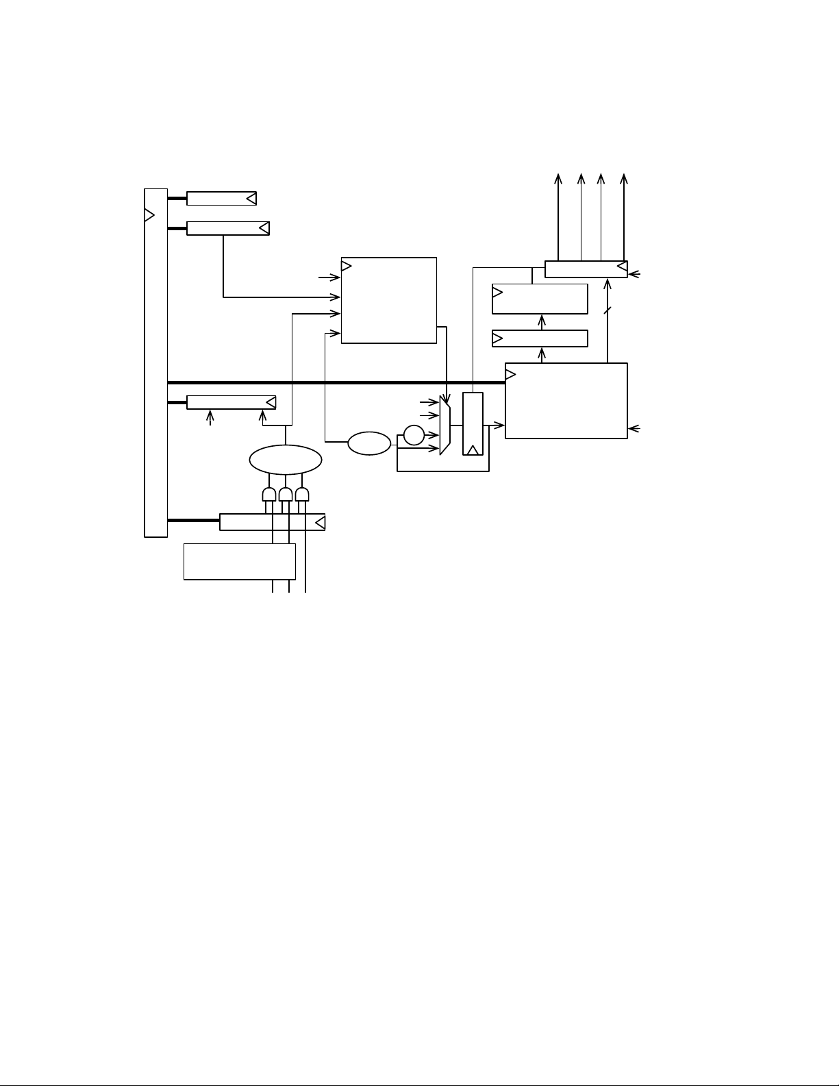
pmui e
dwakeup
awakeup
pmu_out _ 0
hf cl kr st
cor erst
rt ccmpi p
pmuprogram
pmucause
AON TileLink
pmukey
Signal Condition/
Synchronize
reset cause
pmuupc
+1
sleep µPC
wakeup µPC
del ay
Countdown 2
N
end?
PMU State
Machine
aonrst
aonrst
pmusl eep
wakeup?
aonrst
sleep
wakeup
done
pmu_out _ 1
Copyright © 2019, SiFive Inc. All rights reserved. 66
15.1 PMU Overview
The PMU is a synchronous unit clocked by the lfClk in the AON domain. The PMU handles
reset, wakeup, and sleep actions initiated by power-on reset, wakeup events, and sleep
requests. When the MOFF block is powered off, the PMU monitors AON signals to initiate the
Figure 7: FE310-G002 Power-Management Unit
wakeup sequence. When the MOFF block is powered on, the PMU awaits sleep requests from
the MOFF block, which initiate the sleep sequence. The PMU is based around a simple programmable microcode sequencer that steps through short programs to sequence output signals
that control the power supplies and reset signals to the clocks, core, and pads in the system.
15.2 Memory Map
The memory map for the PMU is shown in Table 39. The memory map has been designed to
only require naturally aligned 32-bit memory accesses.

Copyright © 2019, SiFive Inc. All rights reserved. 67
Offset Name Description
0x100 pmuwakeupi0 Wakeup program instruction 0
0x104 pmuwakeupi1 Wakeup program instruction 1
0x108 pmuwakeupi2 Wakeup program instruction 2
0x10C pmuwakeupi3 Wakeup program instruction 3
0x110 pmuwakeupi4 Wakeup program instruction 4
0x114 pmuwakeupi5 Wakeup program instruction 5
0x118 pmuwakeupi6 Wakeup program instruction 6
0x11C pmuwakeupi7 Wakeup program instruction 7
0x120 pmusleepi0 Sleep program instruction 0
0x124 pmusleepi1 Sleep program instruction 1
0x128 pmusleepi2 Sleep program instruction 2
0x12C pmusleepi3 Sleep program instruction 3
0x130 pmusleepi4 Sleep program instruction 4
0x134 pmusleepi5 Sleep program instruction 5
0x138 pmusleepi6 Sleep program instruction 6
0x13C pmusleepi7 Sleep program instruction 7
0x140 pmuie PMU Interrupt Enables
0x144 pmucause PMU Wakeup Cause
0x148 pmusleep Initiate PMU Sleep Sequence
0x14C pmukey PMU Key. Reads as 1 when PMU is unlocked
Table 39: PMU Memory Map
15.3 PMU Key Register (pmukey)
The pmukey register has one bit of state. To prevent spurious sleep or PMU program modification, all writes to PMU registers must be preceded by an unlock operation to the pmukey register
location, which sets pmukey to 1. The value 0x51F15E must be written to the pmukey register
address to set the state bit before any write access to any other PMU register. The state bit is
reset at AON reset, and after any write to a PMU register.
PMU registers may be read without setting pmukey.
15.4 PMU Program
The PMU is implemented as a programmable sequencer to support customization and tuning of
the wakeup and sleep sequences. A wakeup or sleep program comprises eight instructions. An
instruction consists of a delay, encoded as a binary order of magnitude, and a new value for all
of the PMU output signals to assume after that delay. The PMU instruction format is shown in
Table 40. For example, the instruction 0x108 delays for clock cycles, then raises hfclkrst
and lowers all other output signals.
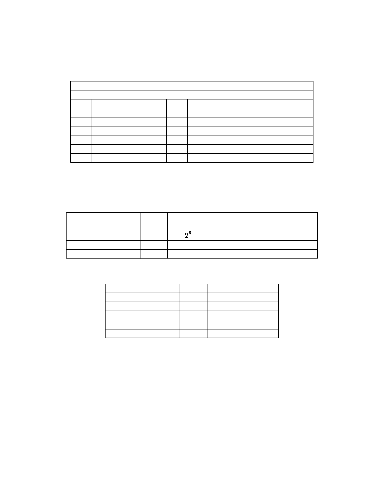
Copyright © 2019, SiFive Inc. All rights reserved. 68
The PMU output signals are registered and only toggle on PMU instruction boundaries. The output registers are all asynchronously set to 1 by aonrst.
PMU Instruction Format (pmu(sleep/wakeup)iX)
Register Offset 0x100
Bits Field Name Attr. Rst. Description
[3:0] delay RW X delay multiplier
4 pmu_out_0_en RW X Drive PMU Output En 0 High
5 pmu_out_1_en RW X Drive PMU Output En 1 High
7 corerst RW X Core Reset
8 hfclkrst RW X High-Frequency Clock Reset
9 isolate RW X Isolate MOFF-to-AON Power Domains
Table 40: PMU Instruction Format
At power-on reset, the PMU program memories are reset to conservative defaults. Table 41
shows the default wakeup program, and Table 42 shows the default sleep program.
Program Instruction Value Meaning
0 0x3F0 Assert all resets and enable all power supplies
1 0x2F8
2 0x030 Deassert corerst and padrst
3-7 0x030 Repeats
Table 41: Default PMU wakeup program
Idle
cycles, then deassert hfclkrst
Program Instruction Value Meaning
0 0x2F0 Assert corerst
1 0x3F0 Assert hfclkrst
2 0x3D0 Deassert pmu_out_1
3 0x3C0 Deassert pmu_out_0
4-7 0x3C0 Repeats
Table 42: Default PMU sleep program
15.5 Initiate Sleep Sequence Register (pmusleep)
Writing any value to the pmusleep register initiates the sleep sequence stored in the sleep program memory. The MOFF block will sleep until an event enabled in the pmuie register occurs.
15.6 Wakeup Signal Conditioning
The PMU can be woken by the external dwakeup signal, which is preconditioned by the signal
conditioning block.

Copyright © 2019, SiFive Inc. All rights reserved. 69
The dwakeup signal has a fixed deglitch circuit that requires the dwakeup signal remain asserted
for two AON clock edges before being accepted. The conditioning circuit also resynchronizes
the dwakeup signal to the AON lfclk.
15.7 PMU Interrupt Enables (pmuie) and Wakeup Cause (pmucause)
The pmuie register indicates which events can wake the MOFF block from sleep.
The dwakeup bit indicates that a logic 0 on the dwakeup_n pin can rouse MOFF. The rtc bit
indicates that the RTC comparator can rouse MOFF.
pmuie: PMU Interrupt Enables (pmuie)
Register Offset 0x140
Bits Field Name Attr. Rst. Description
[3:0] pmuie RW 0x1 PMU Interrupt Enables
[31:4] Reserved
Table 43: pmuie: PMU Interrupt Enables
Following a wakeup, the pmucause register indicates which event caused the wakeup. The
value in the wakeupcause field corresponds to the bit position of the event in pmuie, e.g., a
value of 2 indicates dwakeup. The value 0 indicates a wakeup from reset. These causes are
shown in Table 45.
In the event of a wakeup from reset, the resetcause field indicates which reset source triggered
the wakeup. Table 46 lists the values the resetcause field may take. The value in resetcause
persists until the next reset.
pmucause: PMU Wakeup Cause (pmucause)
Register Offset 0x144
Bits Field Name Attr. Rst. Description
[31:0] pmucause RO X PMU Wakeup Cause
Table 44: pmucause: PMU Wakeup Cause
Index Meaning
0 Reset
1 RTC Wakup (rtc)
2 Digitial input wakeup (dwakeup)
Table 45: Wakeup cause values

Copyright © 2019, SiFive Inc. All rights reserved. 70
Index Meaning
0 Power-on Reset
1 External reset
2 Watchdog timer reset
Table 46: Reset cause values
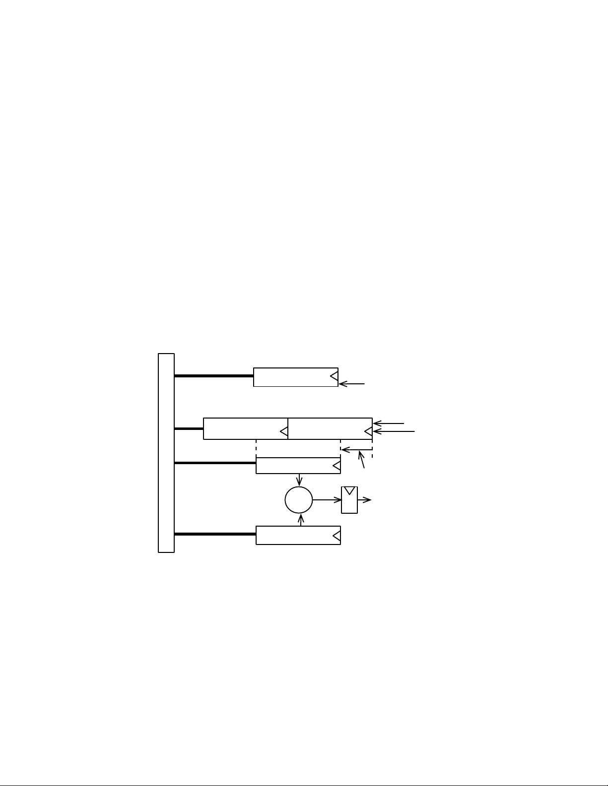
Chapter 16
rt ccmp
rt chi
rt ccf g
AON TileLink
rt ccmpi p
l f cl k
aonrst
rt cl o
rt cs
rt cen
rt cscal e
>=?
Real-Time Clock (RTC)
The real-time clock (RTC) is located in the always-on domain, and is clocked by a selectable
low-frequency clock source. For best accuracy, the RTC should be driven by an external
32.768 kHz watch crystal oscillator, but to reduce system cost, can be driven by a factorytrimmed on-chip oscillator.
Figure 8: Real-Time Clock
16.1 RTC Count Registers (rtccounthi/rtccountlo)
The real-time counter is based around the rtccounthi/rtccountlo register pair, which increment at the low-frequency clock rate when the RTC is enabled. The rtccountlo register holds
the low 32 bits of the RTC, while rtccounthi holds the upper 16 bits of the RTC value. The
total ≥48-bit counter width ensures there will no counter rollover for over 270 years assuming a
32.768 kHz low-frequency real-time clock source. The counter registers can be read or written
over the TileLink bus.
71

Copyright © 2019, SiFive Inc. All rights reserved. 72
rtccounthi: High bits of Counter (rtccounthi)
Register Offset 0x4C
Bits Field Name Attr. Rst. Description
[31:0] rtccounthi RW X High bits of Counter
Table 47: rtccounthi: High bits of Counter
rtccountlo: Low bits of Counter (rtccountlo)
Register Offset 0x48
Bits Field Name Attr. Rst. Description
[31:0] rtccountlo RW X Low bits of Counter
Table 48: rtccountlo: Low bits of Counter
16.2 RTC Configuration Register (rtccfg)
rtccfg: rtc Configuration (rtccfg)
Register Offset 0x40
Bits Field Name Attr. Rst. Description
[3:0] rtcscale RW X Counter scale value.
[11:4] Reserved
12 rtcenalways RW 0x0 Enable Always - run continuously
[27:13] Reserved
28 rtcip0 RW X Interrupt 0 Pending
[31:29] Reserved
Table 49: rtccfg: rtc Configuration
The rtcenalways bit controls whether the RTC is enabled, and is reset on AON reset.
The 4-bit rtcscale field scales the real-time counter value before feeding to the real-time interrupt comparator. The value in rtcscale is the bit position within the rtccountlo/rtccounthi
register pair of the start of a 32-bit field rtcs. A value of 0 in rtcscale indicates no scaling, and
rtcs would then be equal to rtclo. The maximum value of 15 in rtcscale corresponds to
dividing the clock rate by
ment once per second. The value of rtcs is memory-mapped and can be read as a single
32-bit register over the AON TileLink bus.
, so for an input clock of 32.768 kHz, the LSB of rtcs will incre-
16.3 RTC Compare Register (rtccmp)
The rtccmp register holds a 32-bit value that is compared against rtcs, the scaled real-time
clock counter. If rtcs is greater than or equal to rtccmp, the rtccmpip interrupt pending bit is
set. The rtccmpip interrupt pending bit is read-only. The rtccmpip bit can be cleared down by
writing a value to rtccmp that is greater than rtcs.

Copyright © 2019, SiFive Inc. All rights reserved. 73
rtccmp0: Comparator 0 (rtccmp0)
Register Offset 0x60
Bits Field Name Attr. Rst. Description
[31:0] rtccmp0 RW X Comparator 0
Table 50: rtccmp0: Comparator 0

Chapter 17
General Purpose Input/Output Controller
(GPIO)
This chapter describes the operation of the General Purpose Input/Output Controller (GPIO) on
the FE310-G002. The GPIO controller is a peripheral device mapped in the internal memory
map. It is responsible for low-level configuration of actual GPIO pads on the device (direction,
pull up-enable, and drive value ), as well as selecting between various sources of the controls
for these signals. The GPIO controller allows separate configuration of each of ngpio GPIO bits.
Figure 9 shows the control structure for each pin.
Atomic operations such as toggles are natively possible with the RISC-V 'A' extension.
74

Copyright © 2019, SiFive Inc. All rights reserved. 75
Figure 9: Structure of a single GPIO Pin with Control Registers. This structure is repeated for
each pin.

Copyright © 2019, SiFive Inc. All rights reserved. 76
17.1 GPIO Instance in FE310-G002
FE310-G002 contains one GPIO instance. Its address and parameters are shown in Table 51.
Instance Number Address ngpio
0 0x10012000 32
Table 51: GPIO Instance
17.2 Memory Map
The memory map for the GPIO control registers is shown in Table 52. The GPIO memory map
has been designed to require only naturally-aligned 32-bit memory accesses. Each register is
ngpio bits wide.
Offset Name Description
0x00 input_val Pin value
0x04 input_en Pin input enable*
0x08 output_en Pin output enable*
0x0C output_val Output value
0x10 pue Internal pull-up enable*
0x14 ds Pin drive strength
0x18 rise_ie Rise interrupt enable
0x1C rise_ip Rise interrupt pending
0x20 fall_ie Fall interrupt enable
0x24 fall_ip Fall interrupt pending
0x28 high_ie High interrupt enable
0x2C high_ip High interrupt pending
0x30 low_ie Low interrupt enable
0x34 low_ip Low interrupt pending
0x40 out_xor Output XOR (invert)
Table 52: GPIO Peripheral Register Offsets. Only naturally aligned 32-bit memory accesses
are supported. Registers marked with an * are asynchronously reset to 0. All other registers are
synchronously reset to 0.
17.3 Input / Output Values
The GPIO can be configured on a bitwise fashion to represent inputs and/or outputs, as set by
the input_en and output_en registers. Writing to the output_val register updates the bits
regardless of the tristate value. Reading the output_val register returns the written value.
Reading the input_val register returns the actual value of the pin gated by input_en.

Copyright © 2019, SiFive Inc. All rights reserved. 77
17.4 Interrupts
A single interrupt bit can be generated for each GPIO bit. The interrupt can be driven by rising
or falling edges, or by level values, and interrupts can be enabled for each GPIO bit individually.
Inputs are synchronized before being sampled by the interrupt logic, so the input pulse width
must be long enough to be detected by the synchronization logic.
To enable an interrupt, set the corresponding bit in the rise_ie and/or fall_ie to 1. If the corresponding bit in rise_ip or fall_ip is set, an interrupt pin is raised.
Once the interrupt is pending, it will remain set until a 1 is written to the *_ip register at that bit.
The interrupt pins may be routed to the PLIC or directly to local interrupts.
17.5 Internal Pull-Ups
When configured as inputs, each pin has an internal pull-up which can be enabled by software.
At reset, all pins are set as inputs, and pull-ups are disabled.
17.6 Drive Strength
When configured as output, each pin has a software-controllable drive strength.
17.7 Output Inversion
When configured as an output (either software or IOF controlled), the software-writable out_xor
register is combined with the output to invert it.
17.8 HW I/O Functions (IOF)
Each GPIO pin can implement up to 2 HW-Driven functions (IOF) enabled with the iof_en register. Which IOF is used is selected with the iof_sel register.
When a pin is set to perform an IOF, it is possible that the software registers port, output_en,
pullup, ds, input_en may not be used to control the pin directly. Rather, the pins may be con-
trolled by hardware driving the IOF. Which functionalities are controlled by the IOF and which
are controlled by the software registers are fixed in the hardware on a per-IOF basis. Those that
are not controlled by the hardware continue to be controlled by the software registers.
If there is no IOFx for a pin configured with IOFx, the pin reverts to full software control.

Copyright © 2019, SiFive Inc. All rights reserved. 78
GPIO Number IOF0 IOF1
0 PWM0_PWM0
1 PWM0_PWM1
2 SPI1_CS0 PWM0_PWM2
3 SPI1_DQ0 PWM0_PWM3
4 SPI1_DQ1
5 SPI1_SCK
6 SPI1_DQ2
7 SPI1_DQ3
8 SPI1_CS1
9 SPI1_CS2
10 SPI1_CS3 PWM2_PWM0
11 PWM2_PWM1
12 I2C0_SDA PWM2_PWM2
13 I2C0_SCL PWM2_PWM3
14
15
16 UART0_RX
17 UART0_TX
18 UART1_TX
19 PWM1_PWM1
20 PWM1_PWM0
21 PWM1_PWM2
22 PWM1_PWM3
23 UART1_RX
24
25
26 SPI2_CS0
27 SPI2_DQ0
28 SPI2_DQ1
29 SPI2_SCK
30 SPI2_DQ2
31 SPI2_DQ3
Table 53: GPIO IOF Mapping

Chapter 18
Universal Asynchronous Receiver/
Transmitter (UART)
This chapter describes the operation of the SiFive Universal Asynchronous Receiver/Transmitter (UART).
18.1 UART Overview
The UART peripheral supports the following features:
• 8-N-1 and 8-N-2 formats: 8 data bits, no parity bit, 1 start bit, 1 or 2 stop bits
• 8-entry transmit and receive FIFO buffers with programmable watermark interrupts
• 16× Rx oversampling with 2/3 majority voting per bit
The UART peripheral does not support hardware flow control or other modem control signals, or
synchronous serial data transfers.
18.2 UART Instances in FE310-G002
FE310-G002 contains two UART instances. Their addresses and parameters are shown in
Table 54.
Instance Num-
ber
0 0x10013000 16 3 8 8
1 0x10023000 16 3 8 8
Address div_width div_init TX FIFO
Depth
Table 54: UART Instances
79
RX FIFO
Depth

Copyright © 2019, SiFive Inc. All rights reserved. 80
18.3 Memory Map
The memory map for the UART control registers is shown in Table 55. The UART memory map
has been designed to require only naturally aligned 32-bit memory accesses.
Offset Name Description
0x00 txdata Transmit data register
0x04 rxdata Receive data register
0x08 txctrl Transmit control register
0x0C rxctrl Receive control register
0x10 ie UART interrupt enable
0x14 ip UART interrupt pending
0x18 div Baud rate divisor
Table 55: Register offsets within UART memory map
18.4 Transmit Data Register (txdata)
Writing to the txdata register enqueues the character contained in the data field to the transmit
FIFO if the FIFO is able to accept new entries. Reading from txdata returns the current value of
the full flag and zero in the data field. The full flag indicates whether the transmit FIFO is
able to accept new entries; when set, writes to data are ignored. A RISC‑V amoor.w instruction
can be used to both read the full status and attempt to enqueue data, with a non-zero return
value indicating the character was not accepted.
Transmit Data Register (txdata)
Register Offset 0x0
Bits Field Name Attr. Rst. Description
[7:0] data RW X Transmit data
[30:8] Reserved
31 full RO X Transmit FIFO full
Table 56: Transmit Data Register
18.5 Receive Data Register (rxdata)
Reading the rxdata register dequeues a character from the receive FIFO and returns the value
in the data field. The empty flag indicates if the receive FIFO was empty; when set, the data
field does not contain a valid character. Writes to rxdata are ignored.

Copyright © 2019, SiFive Inc. All rights reserved. 81
Receive Data Register (rxdata)
Register Offset 0x4
Bits Field Name Attr. Rst. Description
[7:0] data RO X Received data
[30:8] Reserved
31 empty RO X Receive FIFO empty
Table 57: Receive Data Register
18.6 Transmit Control Register (txctrl)
The read-write txctrl register controls the operation of the transmit channel. The txen bit controls whether the Tx channel is active. When cleared, transmission of Tx FIFO contents is suppressed, and the txd pin is driven high.
The nstop field specifies the number of stop bits: 0 for one stop bit and 1 for two stop bits.
The txcnt field specifies the threshold at which the Tx FIFO watermark interrupt triggers.
The txctrl register is reset to 0.
Transmit Control Register (txctrl)
Register Offset 0x8
Bits Field Name Attr. Rst. Description
0 txen RW 0x0 Transmit enable
1 nstop RW 0x0 Number of stop bits
[15:2] Reserved
[18:16] txcnt RW 0x0 Transmit watermark level
[31:19] Reserved
Table 58: Transmit Control Register
18.7 Receive Control Register (rxctrl)
The read-write rxctrl register controls the operation of the receive channel. The rxen bit controls whether the Rx channel is active. When cleared, the state of the rxd pin is ignored, and no
characters will be enqueued into the Rx FIFO.
The rxcnt field specifies the threshold at which the Rx FIFO watermark interrupt triggers.
The rxctrl register is reset to 0. Characters are enqueued when a zero (low) start bit is seen.

Copyright © 2019, SiFive Inc. All rights reserved. 82
Receive Control Register (rxctrl)
Register Offset 0xC
Bits Field Name Attr. Rst. Description
0 rxen RW 0x0 Receive enable
[15:1] Reserved
[18:16] rxcnt RW 0x0 Receive watermark level
[31:19] Reserved
Table 59: Receive Control Register
18.8 Interrupt Registers (ip and ie)
The ip register is a read-only register indicating the pending interrupt conditions, and the readwrite ie register controls which UART interrupts are enabled. ie is reset to 0.
The txwm condition becomes raised when the number of entries in the transmit FIFO is strictly
less than the count specified by the txcnt field of the txctrl register. The pending bit is
cleared when sufficient entries have been enqueued to exceed the watermark.
The rxwm condition becomes raised when the number of entries in the receive FIFO is strictly
greater than the count specified by the rxcnt field of the rxctrl register. The pending bit is
cleared when sufficient entries have been dequeued to fall below the watermark.
UART Interrupt Enable Register (ie)
Register Offset 0x10
Bits Field Name Attr. Rst. Description
0 txwm RW 0x0 Transmit watermark interrupt enable
1 rxwm RW 0x0 Receive watermark interrupt enable
[31:2] Reserved
Table 60: UART Interrupt Enable Register
UART Interrupt Pending Register (ip)
Register Offset 0x14
Bits Field Name Attr. Rst. Description
0 txwm RO X Transmit watermark interrupt pending
1 rxwm RO X Receive watermark interrupt pending
[31:2] Reserved
Table 61: UART Interrupt Pending Register
18.9 Baud Rate Divisor Register (div)
The read-write, div_width-bit div register specifies the divisor used by baud rate generation
for both Tx and Rx channels. The relationship between the input clock and baud rate is given by
the following formula:

Copyright © 2019, SiFive Inc. All rights reserved. 83
The input clock is the bus clock tlclk. The reset value of the register is set to div_init, which
is tuned to provide a 115200 baud output out of reset given the expected frequency of tlclk.
Table 62 shows divisors for some common core clock rates and commonly used baud rates.
Note that the table shows the divide ratios, which are one greater than the value stored in the
div register.
tlclk (MHz) Target Baud (Hz) Divisor Actual Baud (Hz) Error (%)
2 31250 64 31250 0
2 115200 17 117647 2.1
16 31250 512 31250 0
16 115200 139 115107 0.08
16 250000 64 250000 0
200 31250 6400 31250 0
200 115200 1736 115207 0.0064
200 250000 800 250000 0
200 1843200 109 1834862 0.45
384 31250 12288 31250 0
384 115200 3333 115211 0.01
384 250000 1536 250000 0
384 1843200 208 1846153 0.16
Table 62: Common baud rates (MIDI=31250, DMX=250000) and required
divide values to achieve them with given bus clock frequencies. The divide val-
ues are one greater than the value stored in the div register.
The receive channel is sampled at 16× the baud rate, and a majority vote over 3 neighboring
bits is used to determine the received value. For this reason, the divisor must be ≥16 for a
receive channel.
Baud Rate Divisor Register (div)
Register Offset 0x18
Bits Field
Attr. Rst. Description
Name
[15:0] div RW X Baud rate divisor. div_width bits wide, and the reset
value is div_init.
[31:16] Reserved
Table 63: Baud Rate Divisor Register

Chapter 19
Serial Peripheral Interface (SPI)
This chapter describes the operation of the SiFive Serial Peripheral Interface (SPI) controller.
19.1 SPI Overview
The SPI controller supports master-only operation over the single-lane, dual-lane, and quadlane protocols. The baseline controller provides a FIFO-based interface for performing programmed I/O. Software initiates a transfer by enqueuing a frame in the transmit FIFO; when the
transfer completes, the slave response is placed in the receive FIFO.
In addition, a SPI controller can implement a SPI flash read sequencer, which exposes the
external SPI flash contents as a read/execute-only memory-mapped device. Such controllers
are reset to a state that allows memory-mapped reads, under the assumption that the input
clock rate is less than 100 MHz and the external SPI flash device supports the common Winbond/Numonyx serial read (0x03) command. Sequential accesses are automatically combined
into one long read command for higher performance.
The fctrl register controls switching between the memory-mapped and programmed-I/O
modes, if applicable. While in programmed-I/O mode, memory-mapped reads do not access the
external SPI flash device and instead return 0 immediately. Hardware interlocks ensure that the
current transfer completes before mode transitions and control register updates take effect.
19.2 SPI Instances in FE310-G002
FE310-G002 contains three SPI instances. Their addresses and parameters are shown in Table
64.
84

Copyright © 2019, SiFive Inc. All rights reserved. 85
Instance Flash Controller Address cs_width div_width
QSPI 0 Y 0x10014000 1 12
SPI 1 N 0x10024000 4 12
SPI 2 N 0x10034000 1 12
Table 64: SPI Instances
19.3 Memory Map
The memory map for the SPI control registers is shown in Table 65. The SPI memory map has
been designed to require only naturally-aligned 32-bit memory accesses.

Copyright © 2019, SiFive Inc. All rights reserved. 86
Offset Name Description
0x00 sckdiv Serial clock divisor
0x04 sckmode Serial clock mode
0x08 Reserved
0x0C Reserved
0x10 csid Chip select ID
0x14 csdef Chip select default
0x18 csmode Chip select mode
0x1C Reserved
0x20 Reserved
0x24 Reserved
0x28 delay0 Delay control 0
0x2C delay1 Delay control 1
0x30 Reserved
0x34 Reserved
0x38 Reserved
0x3C Reserved
0x40 fmt Frame format
0x44 Reserved
0x48 txdata Tx FIFO Data
0x4C rxdata Rx FIFO data
0x50 txmark Tx FIFO watermark
0x54 rxmark Rx FIFO watermark
0x58 Reserved
0x5C Reserved
0x60 fctrl SPI flash interface control*
0x64 ffmt SPI flash instruction format*
0x68 Reserved
0x6C Reserved
0x70 ie SPI interrupt enable
0x74 ip SPI interrupt pending
Table 65: Register offsets within the SPI memory map. Registers marked * are present only on
controllers with the direct-map flash interface.
19.4 Serial Clock Divisor Register (sckdiv)
The sckdiv is a div_width-bit register that specifies the divisor used for generating the serial
clock (SCK). The relationship between the input clock and SCK is given by the following formula:

Copyright © 2019, SiFive Inc. All rights reserved. 87
The input clock is the bus clock tlclk. The reset value of the div field is 0x3.
Serial Clock Divisor Register (sckdiv)
Register Offset 0x0
Bits Field Name Attr. Rst. Description
[11:0] div RW 0x3 Divisor for serial clock. div_width bits wide.
[31:12] Reserved
Table 66: Serial Clock Divisor Register
19.5 Serial Clock Mode Register (sckmode)
The sckmode register defines the serial clock polarity and phase. Table 68 and Table 69
describe the behavior of the pol and pha fields, respectively. The reset value of sckmode is 0.
Serial Clock Mode Register (sckmode)
Register Offset 0x4
Bits Field Name Attr. Rst. Description
0 pha RW 0x0 Serial clock phase
1 pol RW 0x0 Serial clock polarity
[31:2] Reserved
Table 67: Serial Clock Mode Register
Value Description
0 Inactive state of SCK is logical 0
1 Inactive state of SCK is logical 1
Table 68: Serial Clock Polarity
Value Description
0 Data is sampled on the leading edge of SCK and shifted on the trailing edge of SCK
1 Data is shifted on the leading edge of SCK and sampled on the trailing edge of SCK
Table 69: Serial Clock Phase
19.6 Chip Select ID Register (csid)
The csid is a
by hardware chip select control. The reset value is 0x0.
-bit register that encodes the index of the CS pin to be toggled

Copyright © 2019, SiFive Inc. All rights reserved. 88
Chip Select ID Register (csid)
Register Offset 0x10
Bits Field Name Attr. Rst. Description
[31:0] csid RW 0x0
Table 70: Chip Select ID Register
Chip select ID.
bits wide.
19.7 Chip Select Default Register (csdef)
The csdef register is a cs_width-bit register that specifies the inactive state (polarity) of the CS
pins. The reset value is high for all implemented CS pins.
Chip Select Default Register (csdef)
Register Offset 0x14
Bits Field
Name
[31:0] csdef RW 0x1 Chip select default value. cs_width bits wide, reset to
Attr. Rst. Description
all-1s.
Table 71: Chip Select Default Register
19.8 Chip Select Mode Register (csmode)
The csmode register defines the hardware chip select behavior as described in Table 72. The
reset value is 0x0 (AUTO). In HOLD mode, the CS pin is deasserted only when one of the following conditions occur:
• A different value is written to csmode or csid.
• A write to csdef changes the state of the selected pin.
• Direct-mapped flash mode is enabled.
Chip Select Mode Register (csmode)
Register Offset 0x18
Bits Field Name Attr. Rst. Description
[1:0] mode RW 0x0 Chip select mode
[31:2] Reserved
Table 72: Chip Select Mode Register
Value Name Description
0 AUTO Assert/deassert CS at the beginning/end of each frame
2 HOLD Keep CS continuously asserted after the initial frame
3 OFF Disable hardware control of the CS pin
Table 73: Chip Select Modes

Copyright © 2019, SiFive Inc. All rights reserved. 89
19.9 Delay Control Registers (delay0 and delay1)
The delay0 and delay1 registers allow for the insertion of arbitrary delays specified in units of
one SCK period.
The cssck field specifies the delay between the assertion of CS and the first leading edge of
SCK. When sckmode.pha = 0, an additional half-period delay is implicit. The reset value is 0x1.
The sckcs field specifies the delay between the last trailing edge of SCK and the deassertion of
CS. When sckmode.pha = 1, an additional half-period delay is implicit. The reset value is 0x1.
The intercs field specifies the minimum CS inactive time between deassertion and assertion.
The reset value is 0x1.
The interxfr field specifies the delay between two consecutive frames without deasserting
CS. This is applicable only when sckmode is HOLD or OFF. The reset value is 0x0.
Delay Control Register 0 (delay0)
Register Offset 0x28
Bits Field Name Attr. Rst. Description
[7:0] cssck RW 0x1 CS to SCK Delay
[15:8] Reserved
[23:16] sckcs RW 0x1 SCK to CS Delay
[31:24] Reserved
Table 74: Delay Control Register 0
Delay Control Register 1 (delay1)
Register Offset 0x2C
Bits Field Name Attr. Rst. Description
[7:0] intercs RW 0x1 Minimum CS inactive time
[15:8] Reserved
[23:16] interxfr RW 0x0 Maximum interframe delay
[31:24] Reserved
Table 75: Delay Control Register 1
19.10 Frame Format Register (fmt)
The fmt register defines the frame format for transfers initiated through the programmed-I/O
(FIFO) interface. Table 77, Table 78, and Table 79 describe the proto, endian, and dir fields,
respectively. The len field defines the number of bits per frame, where the allowed range is 0 to
8 inclusive.

Copyright © 2019, SiFive Inc. All rights reserved. 90
For flash-enabled SPI controllers, the reset value is 0x0008_0008, corresponding to proto =
single, dir = Tx, endian = MSB, and len = 8. For non-flash-enabled SPI controllers, the reset
value is 0x0008_0000, corresponding to proto = single, dir = Rx, endian = MSB, and len = 8.
Frame Format Register (fmt)
Register Offset 0x40
Bits Field
Attr. Rst. Description
Name
[1:0] proto RW 0x0 SPI protocol
2 endian RW 0x0 SPI endianness
3 dir RW X SPI I/O direction. This is reset to 1 for flash-enabled SPI
controllers, 0 otherwise.
[15:4] Reserved
[19:16] len RW 0x8 Number of bits per frame
[31:20] Reserved
Table 76: Frame Format Register
Value Description Data Pins
0 Single DQ0 (MOSI), DQ1 (MISO)
1 Dual DQ0, DQ1
2 Quad DQ0, DQ1, DQ2, DQ3
Table 77: SPI Protocol. Unused DQ pins are tri-stated.
Value Description
0 Transmit most-significant bit (MSB) first
1 Transmit least-significant bit (LSB) first
Table 78: SPI Endianness
Value Description
0 Rx: For dual and quad protocols, the DQ pins are tri-stated. For the single protocol,
the DQ0 pin is driven with the transmit data as normal.
1 Tx: The receive FIFO is not populated.
Table 79: SPI I/O Direction
19.11 Transmit Data Register (txdata)
Writing to the txdata register loads the transmit FIFO with the value contained in the data field.
For fmt.len < 8, values should be left-aligned when fmt.endian = MSB and right-aligned
when fmt.endian = LSB.

Copyright © 2019, SiFive Inc. All rights reserved. 91
The full flag indicates whether the transmit FIFO is ready to accept new entries; when set,
writes to txdata are ignored. The data field returns 0x0 when read.
Transmit Data Register (txdata)
Register Offset 0x48
Bits Field Name Attr. Rst. Description
[7:0] data RW 0x0 Transmit data
[30:8] Reserved
31 full RO X FIFO full flag
Table 80: Transmit Data Register
19.12 Receive Data Register (rxdata)
Reading the rxdata register dequeues a frame from the receive FIFO. For fmt.len < 8, values
are left-aligned when fmt.endian = MSB and right-aligned when fmt.endian = LSB.
The empty flag indicates whether the receive FIFO contains new entries to be read; when set,
the data field does not contain a valid frame. Writes to rxdata are ignored.
Receive Data Register (rxdata)
Register Offset 0x4C
Bits Field Name Attr. Rst. Description
[7:0] data RO X Received data
[30:8] Reserved
31 empty RW X FIFO empty flag
Table 81: Receive Data Register
19.13 Transmit Watermark Register (txmark)
The txmark register specifies the threshold at which the Tx FIFO watermark interrupt triggers.
The reset value is 1 for flash-enabled SPI controllers, and 0 for non-flash-enabled SPI controllers.
Transmit Watermark Register (txmark)
Register Offset 0x50
Bits Field
Name
[2:0] txmark RW X Transmit watermark. The reset value is 1 for flash-enabled
[31:3] Reserved
Attr. Rst. Description
controllers, 0 otherwise.
Table 82: Transmit Watermark Register

Copyright © 2019, SiFive Inc. All rights reserved. 92
19.14 Receive Watermark Register (rxmark)
The rxmark register specifies the threshold at which the Rx FIFO watermark interrupt triggers.
The reset value is 0x0.
Receive Watermark Register (rxmark)
Register Offset 0x54
Bits Field Name Attr. Rst. Description
[2:0] rxmark RW 0x0 Receive watermark
[31:3] Reserved
Table 83: Receive Watermark Register
19.15 SPI Interrupt Registers (ie and ip)
The ie register controls which SPI interrupts are enabled, and ip is a read-only register indicating the pending interrupt conditions. ie is reset to zero. See Table 84.
The txwm condition becomes raised when the number of entries in the transmit FIFO is strictly
less than the count specified by the txmark register. The pending bit is cleared when sufficient
entries have been enqueued to exceed the watermark. See Table 85.
The rxwm condition becomes raised when the number of entries in the receive FIFO is strictly
greater than the count specified by the rxmark register. The pending bit is cleared when sufficient entries have been dequeued to fall below the watermark. See Table 85.
SPI Interrupt Enable Register (ie)
Register Offset 0x70
Bits Field Name Attr. Rst. Description
0 txwm RW 0x0 Transmit watermark enable
1 rxwm RW 0x0 Receive watermark enable
[31:2] Reserved
Table 84: SPI Interrupt Enable Register
SPI Watermark Interrupt Pending Register (ip)
Register Offset 0x74
Bits Field Name Attr. Rst. Description
0 txwm RO 0x0 Transmit watermark pending
1 rxwm RO 0x0 Receive watermark pending
[31:2] Reserved
Table 85: SPI Watermark Interrupt Pending Register

Copyright © 2019, SiFive Inc. All rights reserved. 93
19.16 SPI Flash Interface Control Register (fctrl)
When the en bit of the fctrl register is set, the controller enters direct memory-mapped SPI
flash mode. Accesses to the direct-mapped memory region causes the controller to automatically sequence SPI flash reads in hardware. The reset value is 0x1. See Table 86.
SPI Flash Interface Control Register (fctrl)
Register Offset 0x60
Bits Field Name Attr. Rst. Description
0 en RW 0x1 SPI Flash Mode Select
[31:1] Reserved
Table 86: SPI Flash Interface Control Register
19.17 SPI Flash Instruction Format Register (ffmt)
The ffmt register defines the format of the SPI flash read instruction issued by the controller
when the direct-mapped memory region is accessed while in SPI flash mode.
An instruction consists of a command byte followed by a variable number of address bytes,
dummy cycles (padding), and data bytes. Table 87 describes the function and reset value of
each field.
SPI Flash Instruction Format Register (ffmt)
Register Offset 0x64
Bits Field Name Attr. Rst. Description
0 cmd_en RW 0x1 Enable sending of command
[3:1] addr_len RW 0x3 Number of address bytes (0 to 4)
[7:4] pad_cnt RW 0x0 Number of dummy cycles
[9:8] cmd_proto RW 0x0 Protocol for transmitting command
[11:10] addr_proto RW 0x0 Protocol for transmitting address and padding
[13:12] data_proto RW 0x0 Protocol for receiving data bytes
[15:14] Reserved
[23:16] cmd_code RW 0x3 Value of command byte
[31:24] pad_code RW 0x0 First 8 bits to transmit during dummy cycles
Table 87: SPI Flash Instruction Format Register

Chapter 20
Pulse Width Modulator (PWM)
This chapter describes the operation of the Pulse-Width Modulation peripheral (PWM).
20.1 PWM Overview
Figure 10 shows an overview of the PWM peripheral. The default configuration described here
has four independent PWM comparators (pwmcmp0–pwmcmp3), but each PWM Peripheral is
parameterized by the number of comparators it has (ncmp). The PWM block can generate multiple types of waveforms on output pins (pwm
forms of internal timer interrupt. The comparator results are captured in the pwmcmp ip flops
and then fed to the PLIC as potential interrupt sources. The pwmcmp
processed by an output ganging stage before being fed to the GPIOs.
PWM instances can support comparator precisions (cmpwidth) up to 16 bits, with the example
described here having the full 16 bits. To support clock scaling, the pwmcount register is 15 bits
wider than the comparator precision cmpwidth.
gpio) and can also be used to generate several
ip outputs are further
94
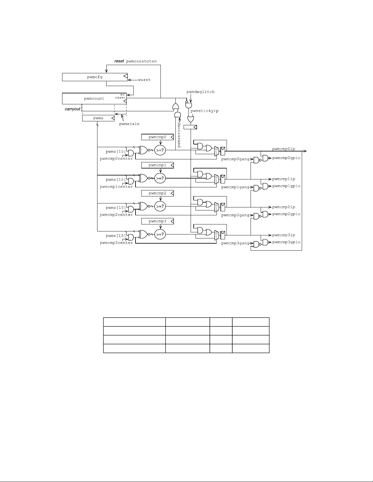
Copyright © 2019, SiFive Inc. All rights reserved. 95
Figure 10: PWM Peripheral
20.2 PWM Instances in FE310-G002
FE310-G002 contains three PWM instances. Their addresses and parameters are shown in
Table 88.
Instance Number Address ncmp cmpwidth
0 0x10015000 4 8
1 0x10025000 4 16
2 0x10035000 4 16
Table 88: PWM Instances
20.3 PWM Memory Map
The memory map for the PWM peripheral is shown in Table 89.
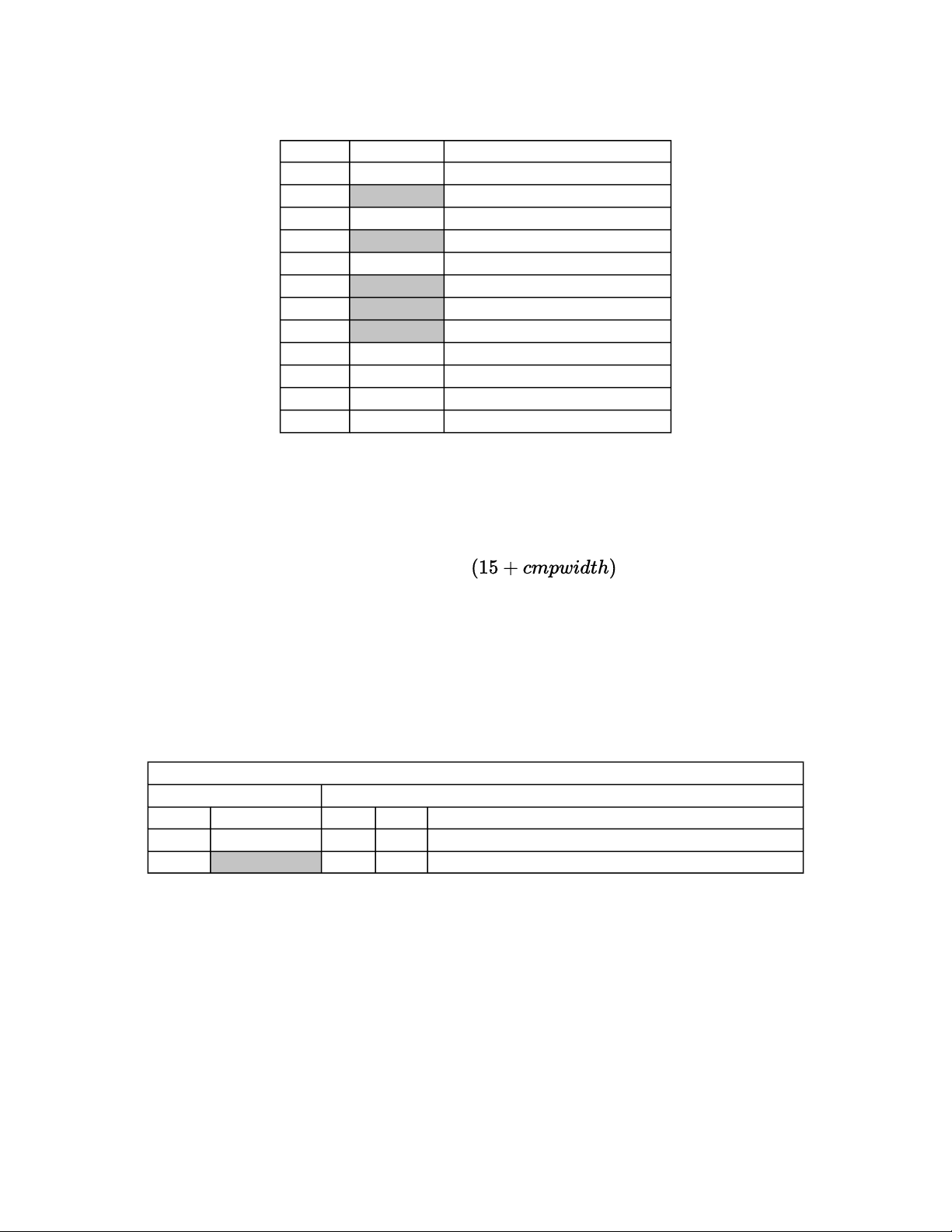
Copyright © 2019, SiFive Inc. All rights reserved. 96
Offset Name Description
0x00 pwmcfg PWM configuration register
0x04 Reserved
0x08 pwmcount PWM count register
0x0C Reserved
0x10 pwms Scaled PWM count register
0x14 Reserved
0x18 Reserved
0x1C Reserved
0x20 pwmcmp0 PWM 0 compare register
0x24 pwmcmp1 PWM 1 compare register
0x28 pwmcmp2 PWM 2 compare register
0x2C pwmcmp3 PWM 3 compare register
Table 89: SiFive PWM memory map, offsets relative to PWM peripheral base address
20.4 PWM Count Register (pwmcount)
The PWM unit is based around a counter held in pwmcount. The counter can be read or written
over the TileLink bus. The pwmcount register is
cmpwidth of 16 bits, the counter is held in pwmcount[30:0], and bit 31 of pwmcount returns a
zero when read.
bits wide. For example, for
When used for PWM generation, the counter is normally incremented at a fixed rate then reset
to zero at the end of every PWM cycle. The PWM counter is either reset when the scaled
counter pwms reaches the value in pwmcmp0, or is simply allowed to wrap around to zero.
The counter can also be used in one-shot mode, where it disables counting after the first reset.
PWM Count Register (pwmcount)
Register Offset 0x8
Bits Field Name Attr. Rst. Description
[30:0] pwmcount RW X PWM count register. cmpwidth + 15 bits wide.
31 Reserved
Table 90: PWM Count Register

Copyright © 2019, SiFive Inc. All rights reserved. 97
20.5 PWM Configuration Register (pwmcfg)
PWM Configuration Register (pwmcfg)
Register Offset 0x0
Bits Field Name Attr. Rst. Description
[3:0] pwmscale RW X PWM Counter scale
[7:4] Reserved
8 pwmsticky RW X PWM Sticky - disallow clearing pwmcmp
9 pwmzerocmp RW X PWM Zero - counter resets to zero after match
10 pwmdeglitch RW X PWM Deglitch - latch pwmcmp
cycle
11 Reserved
12 pwmenalways RW 0x0 PWM enable always - run continuously
13 pwmenoneshot RW 0x0 PWM enable one shot - run one cycle
[15:14] Reserved
16 pwmcmp0center RW X PWM0 Compare Center
17 pwmcmp1center RW X PWM1 Compare Center
18 pwmcmp2center RW X PWM2 Compare Center
19 pwmcmp3center RW X PWM3 Compare Center
[23:20] Reserved
24 pwmcmp0gang RW X PWM0/PWM1 Compare Gang
25 pwmcmp1gang RW X PWM1/PWM2 Compare Gang
26 pwmcmp2gang RW X PWM2/PWM3 Compare Gang
27 pwmcmp3gang RW X PWM3/PWM0 Compare Gang
28 pwmcmp0ip RW X PWM0 Interrupt Pending
29 pwmcmp1ip RW X PWM1 Interrupt Pending
30 pwmcmp2ip RW X PWM2 Interrupt Pending
31 pwmcmp3ip RW X PWM3 Interrupt Pending
ip within same
ip bits
Table 91: PWM Configuration Register
The pwmcfg register contains various control and status information regarding the PWM peripheral, as shown in Table 91.
The pwmen* bits control the conditions under which the PWM counter pwmcount is incremented.
The counter increments by one each cycle only if any of the enabled conditions are true.
If the pwmenalways bit is set, the PWM counter increments continuously. When pwmenoneshot
is set, the counter can increment but pwmenoneshot is reset to zero once the counter resets,
disabling further counting (unless pwmenalways is set). The pwmenoneshot bit provides a way
for software to generate a single PWM cycle then stop. Software can set the pwmenoneshot
again at any time to replay the one-shot waveform. The pwmen* bits are reset at wakeup reset,
which disables the PWM counter and saves power.

Copyright © 2019, SiFive Inc. All rights reserved. 98
The 4-bit pwmscale field scales the PWM counter value before feeding it to the PWM comparators. The value in pwmscale is the bit position within the pwmcount register of the start of a
cmpwidth-bit pwms field. A value of 0 in pwmscale indicates no scaling, and pwms would then be
equal to the low cmpwidth bits of pwmcount. The maximum value of 15 in pwmscale corre-
sponds to dividing the clock rate by 215, so for an input bus clock of 16 MHz, the LSB of pwms
will increment at 488.3 Hz.
The pwmzerocmp bit, if set, causes the PWM counter pwmcount to be automatically reset to zero
one cycle after the pwms counter value matches the compare value in pwmcmp0. This is normally
used to set the period of the PWM cycle. This feature can also be used to implement periodic
counter interrupts, where the period is independent of interrupt service time.
20.6 Scaled PWM Count Register (pwms)
The Scaled PWM Count Register pwms reports the cmpwidth-bit portion of pwmcount which
starts at pwmscale, and is what is used for comparison against the pwmcmp registers.
Scaled PWM Count Register (pwms)
Register Offset 0x10
Bits Field Name Attr. Rst. Description
[15:0] pwms RW X Scaled PWM count register. cmpwidth bits wide.
[31:16] Reserved
Table 92: Scaled PWM Count Register
20.7 PWM Compare Registers (pwmcmp0–pwmcmp3)
PWM 0 Compare Register (pwmcmp0)
Register Offset 0x20
Bits Field Name Attr. Rst. Description
[15:0] pwmcmp0 RW X PWM 0 Compare Value
[31:16] Reserved
Table 93: PWM 0 Compare Register
PWM 1 Compare Register (pwmcmp1)
Register Offset 0x24
Bits Field Name Attr. Rst. Description
[15:0] pwmcmp1 RW X PWM 1 Compare Value
[31:16] Reserved
Table 94: PWM 1 Compare Register
 Loading...