

Page 1

5ED5/5EDM-(T2)
586 CPU Supported PCI Mainboard
User Guide & Technical Reference
Page 2

SOYO
About This Guide
TM
This User’s Guide is for assisting system ma nufacturers a nd end u sers in setting
up and installing the mainboard. Information in this gu ide has been carefully
check ed for reliability; however, no guarantee is given as to the correctness of
the contents. The information in this document is subject to change without
notice.
Copyright 1998, S oyo Computer Inc. All rights reserved. This m anua l i s
copyrighted by Soyo Computer Inc. You may not reproduce, transmit, transcribe,
store in a retrieval system, or translate into any langua ge, in any form or by any
means, electronic, mechanica l, magnetic, optical, chemical, ma nual, or otherwise,
any part of this publication without express written permission of Soyo Computer
Inc.
Soyo is a registered trademark of Soyo Computer Inc. All trademarks are the
property of their owners.
Soyo Computer Inc. ma kes no representations or warranties regard ing the
contents of this manual. We reserve the righ t to revise the manual or make
changes in the specifications of the product described with in it at any time
without notice and without obligation to notify any person of such revision or
change. The information conta ined in this manual is provided for general use by
our customers. Our customers should be aware that the personal computer field is
the subject of many patent s. O ur cust omers s houl d ensure that they tak e
appropria te action so that their use of ou r products does not infringe upon a ny
patents. It is the policy of Soyo Computer Inc.to respect the va lid patent rights of
third parties and not to infringe upon or assist others to infringe u pon such rights.
Use, du plication, or disclosure by the Government is subject to restrictions set
forth in subparagraph ( c )(1)(ii) of the Rights in Technical Data and Computer
Software clause at 252.277-7013.
Product mentioned in this manual are mentioned for identification purpose only.
Product names appearing in this manual may or may not be registered trademarks
or copyrights of their respective companies.
If you need any further information, please come to ou r home page on internet.
The address is “ http://ww.soyo.com.tw”.
Copyright Notice
Trademarks
Di sclai mer
Restricted Rights Legend
Product Rights
Page 3

Table of Contents
Chapter 1: Introduction .................................................. 1
Key Features ............................................................................... 1
Unpacking the Mainboard........................................................... 2
Electrostatic Discharge Precautions............................................ 2
Mainboard Layout w/ Default Settings ....................................... 3
Chapter 2: Hardware Setup ............................................ 5
Jumpers ....................................................................................... 5
JP5: CMOS Clear Jumper .................................................... 5
JP22: CPU Burst Mode Jumper ........................................... 6
JP1: Smart Detect CPU Voltage Auto/Manual Jumper ....... 6
JP37: DIMM Voltage Jumper .............................................. 7
CPU Type Configuration ............................................................ 8
P54C/P55C Series CPUs Settings ......................................... 8
P54C/P55C Series CPUs Settings (Continued) ..................... 9
AMD K5/K6 Series CPUs Setting ...................................... 10
Cyrix 6x86/L/MX Series CPUs Setting .............................. 11
Memory Configuration ............................................................. 12
Memory Configuration Table.............................................. 12
RAM Bank Installation Notice............................................ 12
Cache Configuration ................................................................. 13
Cache Size and RAM Locations ......................................... 13
Multi I/O Port Addresses .......................................................... 13
Connectors ................................................................................ 14
Front Panel Connectors ....................................................... 14
Back Panel Connectors........................................................ 15
Other Connectors................................................................. 15
Chapter 3: BIOS Setup.................................................. 18
Standard CMOS Setup .............................................................. 19
BIOS Features Setup ................................................................. 21
Chipset Features Setup.............................................................. 24
Power Management Setup ........................................................ 26
PNP/PCI Configuration Setup .................................................. 29
Load Setup Defaults.................................................................. 31
Load BIOS Defaults.................................................................. 31
Integrated Peripherals ............................................................... 32
Supervisor Password ................................................................. 34
User Password ........................................................................... 35
IDE HDD Auto Detection ......................................................... 36
Page 4

Quick Instalation Guide… … … … … … … … … … … … … … … ..38
Motherboard Layout………….………………………….……38
CPU Voltage and Frequency Jumper Settings…..…..….…….38
Voltage Settings : JP30…………………………………….38
CPU Frequency Settings : SW1……………………..…….38
Memory Configuration…..……………………………….…...38
Additional Jumper Settings……..………………………..….. 39
Setting for Various Processors : SW1 & JP30..………………39
Drivers Installation Guide… … … … … … … … … .… … … … … .40
South Bridge/IDE Bus Master Drivers……….………………40
Install AGP Card Steps……………………....………….……41
BIOS Update… … … … … .… … … … … … … … … .… … … … … .42
Page 5

1 Introduction
The ETEQ 82C662X PCI mainboard is a high-performance ATX formfactor system board that supports P54C/P55C family CPUs. This
mainboard is fully compatible with industry standards and adds many
technical enhancements.
Key Features
¥CPU
ÑSupports P54C/P55C family CPUs running at 75~233 MHz
speeds; Cyrix 6x86/6x86L/6x86MX CPUs running at
PR150~PR266 speeds; and AMD K5/K6 CPUs running at
P75~PR300 speeds
ÑSupports Socket 7 for upgrade
ÑSupports P54C/P55C series SMM Mode and CPU Stop Clock
ÑSupports MMX technology and Smart Detect CPU Voltage
function
¥L2 Cache Controller
ÑOn-board 512K/1M Pipeline Burst SRAMs Cache
¥DRAM Controller
ÑSupports 2 strips of 72-pin FPM/EDO SIMM (symmetrical/
asymmetrical addressing)
ÑSupports 3 strips of 168-pin EDO/SDRM Unbuffered DIMM
ÑComes with three DIMM banks, supports 8/16/32/64/128 MB
unbuffered DIMMs
ÑMemory configuration for DIMM is from 8MB to 384 MB; for
SIMM is from 8MB to 64MB
¥BUS Controller
ÑCompliant to PCI specifications v2.1
ÑFive 32-bit PCI slots, two ISA slots, and one AGP slot
ÑOnboard USB (Universal Serial Bus) port
¥Peripheral Controller
ÑSystem BIOS include NCR 810 SCSI BIOS and Plug&Play func.
ÑOnboard PCI Master IDE controller and floppy controller
ÑOnboard supports two high speed UARTS (w/i 16550 FIFO), one
ECP/EPP/SPP multi-mode parallel port, and one PS/2 mouse port
ÑOnboard FLASH Memory for easy upgrade BIOS
ÑEasy installation of ETEQ E-IDE/ATAPI CD-ROM Bus Master
Drivers included
ÑOnboard support IR connector
Page 6

2 Introduction
Unpacking the Mainboard
The mainboard package contains:
Ÿ The EQ82C662X Mainboard
Ÿ One CD (Including Manuals/Drivers/Utilities)
Ÿ One page of One Sheet Manual
Note: Do not unpack the mainboard until you are ready to install it.
Follow the precautions below while unpacking the mainboard.
1. Be fore handling the mainboard, ground yourself by grasping an
unpainted portion of the system’s metal chassis.
2. Remove the mainboard from its anti-static packaging and place it on
a grounded surface, component side up.
3. Check the mainboard fo r damage. I f any chip appears loose, press
carefully to seat it firmly in its socket.
Do not apply power if the mainboard appears damaged. If there is
dam a ge t o th e boa rd c onta c t yo ur d e ale r imm edia t ely.
Electrostatic Discharge Precautions
Make sure yo u ground yourself before handling the mainboard or other
syste m components. Electrostatic discharge can easily damage the
components. Note that you must take special precaution when handling
the mainboard in dry or air-conditioned environments.
Take these precautions to protect your equipment from electrostatic
discharge:
Ÿ Do not remove the anti-static packaging until you are ready to install
the mainboard and other system components.
Ÿ Ground yourself before removing any system component from its
protective anti-static packaging. To ground yourself grasp the
expansion
slot covers or other unpainted portions of the computer chassis.
Ÿ Frequently ground yourself while working, or use a grounding strap.
Ÿ Handle the mainboard by the edges and avoid touching its
components.
Page 7
Introduction 3
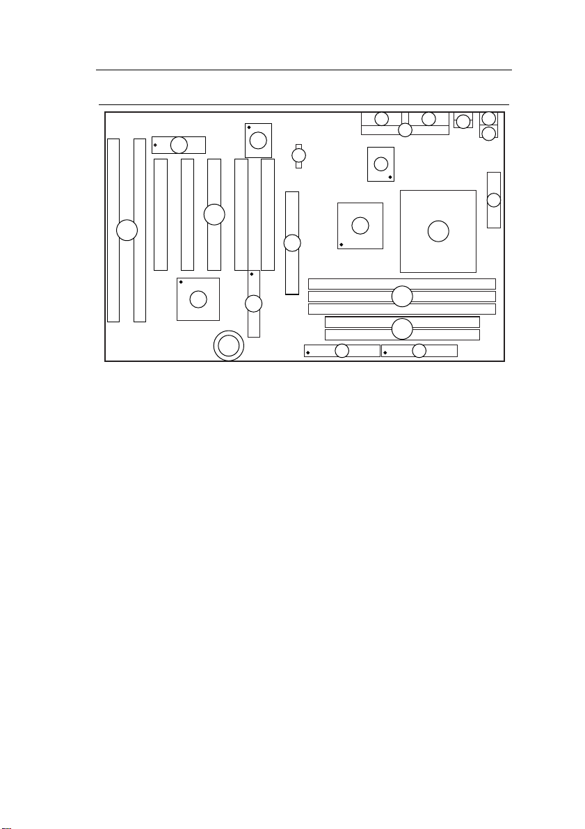
Mainboard Layout w/ Default Settings
14 14
5
8
7
4
6
2
20
13
3
1
16
18
17
15
2
11
9
10
19
12 12
Figure 1Ð1. Mainboard Layout
1.ZIF socket 7 11.Floppy Connector
2.EQ82C662X Chipset 12.IDE1/IDE2 Connector
3.Pipelined Burst SRAM 13.Parallel Port Connector
4.Super I/O Chip 14.COM1/COM2 Connector
5.PnP FLASH BIOS 15.ATX Power Connector
6.1TAG SRAM (or 2 SRAMs) 16.PS/2 KB Connector
7.ISA Slots 17.PS/2 Mouse Connector
8.PCI Slots 18.USB Connectors
9.Unbuffered DIMM Bank 19.3 Volt. Lithium Battery
10.SIMM Bank 20.AGP Port
Page 8
4
Introduction
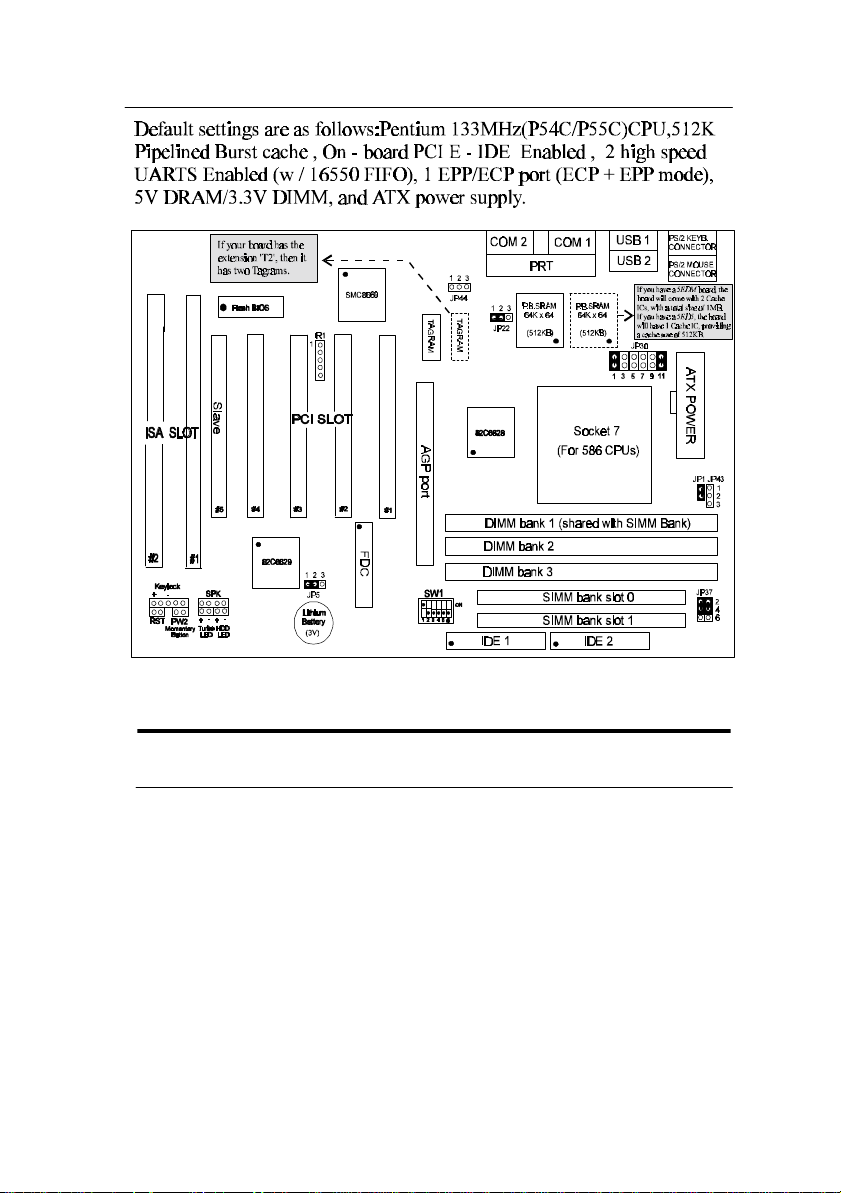
Figure 1-2. Mainboard Default Setting
Important: Make sure the system is well ventilated to prevent
overheating and ensure system stability.
Page 9
2 Hardware Setup
This chapter is designed for Normal edition mainboard use only and it
explains how to configure the mainboardÕs hardware. After you install
the mainboard, you can set jumpers, install memory on the mainboard,
and make case connections. Refer to this chapter whenever you upgrade
or reconfigure your system.
CAUTION: Turn off power to the mainboard, system chassis, and
peripheral devices before performing any work on the
mainboard or system.
Jumpers
This mainboard uses different colors of jumper caps to identify different
functions of the jumpers:
Jumper Cap Color White Black Blue Red Green
clear
Function
CMOS
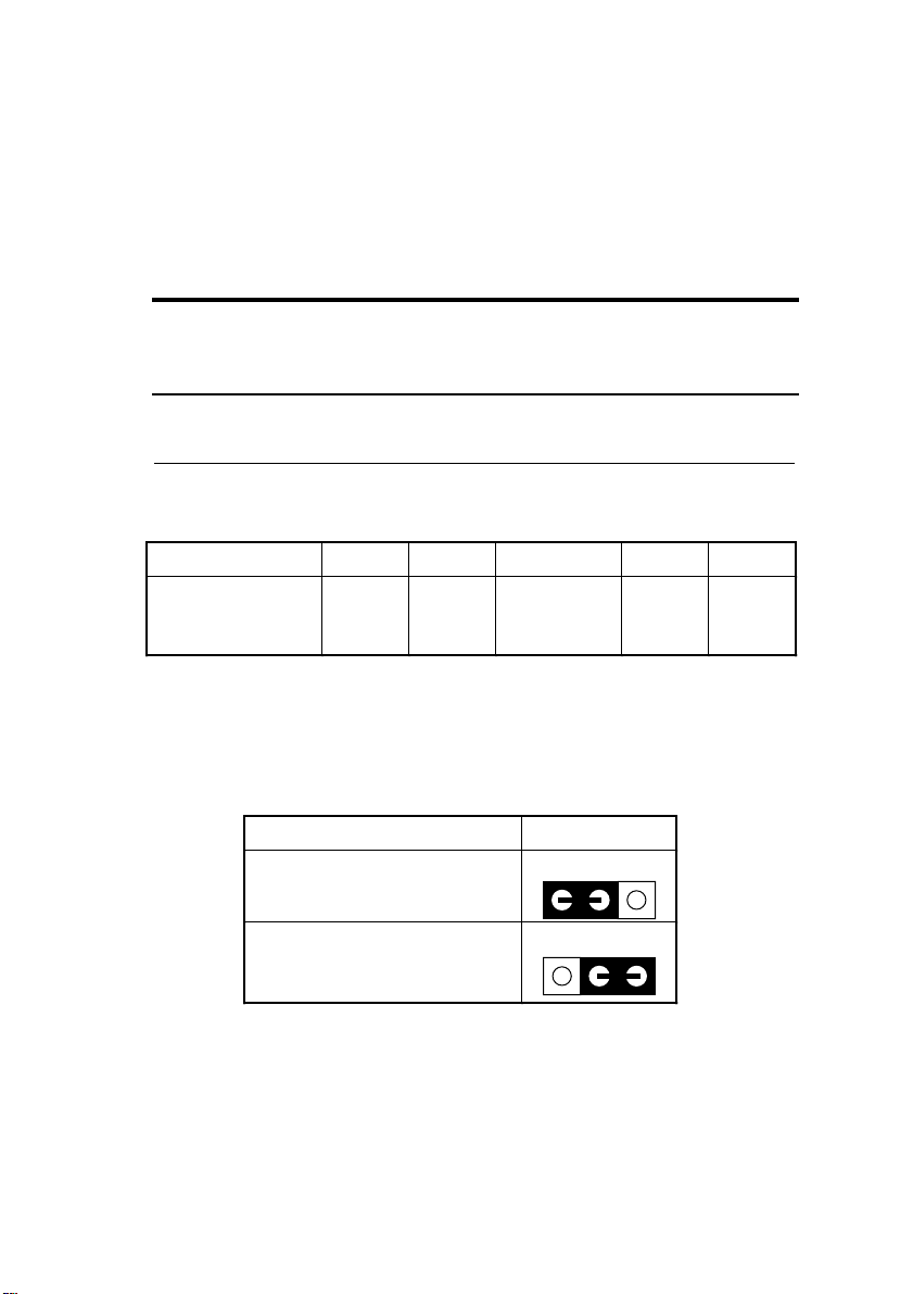
JP5: CMOS Clear Jumper
Clear the CMOS memory by momentarily shorting pin 2Ð3; then
shorting pin 1Ð2 to retain new settings.
CPU
burst
mode
Smart
Detect CPU
voltage
DIMM
voltage
CPU
Voltage
CMOS Setting JP5
Retain CMOS data
(default)
Clear CMOS data
123
123
Page 10
6 Hardware Setup
JP22: CPU Burst Mode Jumper
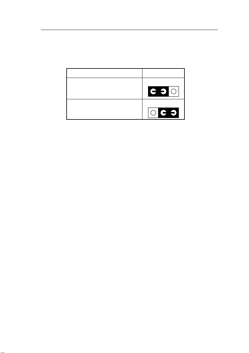
Due to different designs, there are two kinds of CPU burst modes:
Interleave Burst and Linear Burst. Select the correct mode according to
the CPU you are using.
CPU Burst Mode JP22
Interleave
(for P54C/P55C and AMD
K5/K6 CPU)
Linear
(for Cyrix 6x86/L/MX CPU)
When using a Cyrix series of CPUs, follow the below procedures after
select the burst mode:
1. Press<Delete> key to enter the BIOS setup menu during the boot-up,
2. Select ÒChipset Features SetupÓ,
3. Set the ÒLinear BurstÓ to ÒEnabledÓ,
4. Press <Esc> to go back to the main menu and choose ÒSave & Exit
SetupÓ to reboot your computer.
123
123
JP1: Smart Detect CPU Voltage Auto/Manual Jumper
For P54C/P55C and Cyrix 6x86/L CPUs, this board automatically
detects and adjusts the CPU voltage to the proper voltage. JP1 is
reserved for a few older non-Intel CPUs which can not be detect
correctly. If you run into problems while detecting the voltage of older
CPUs, remove the jumper cap to correct it.
Page 11
Hardware Setup 7
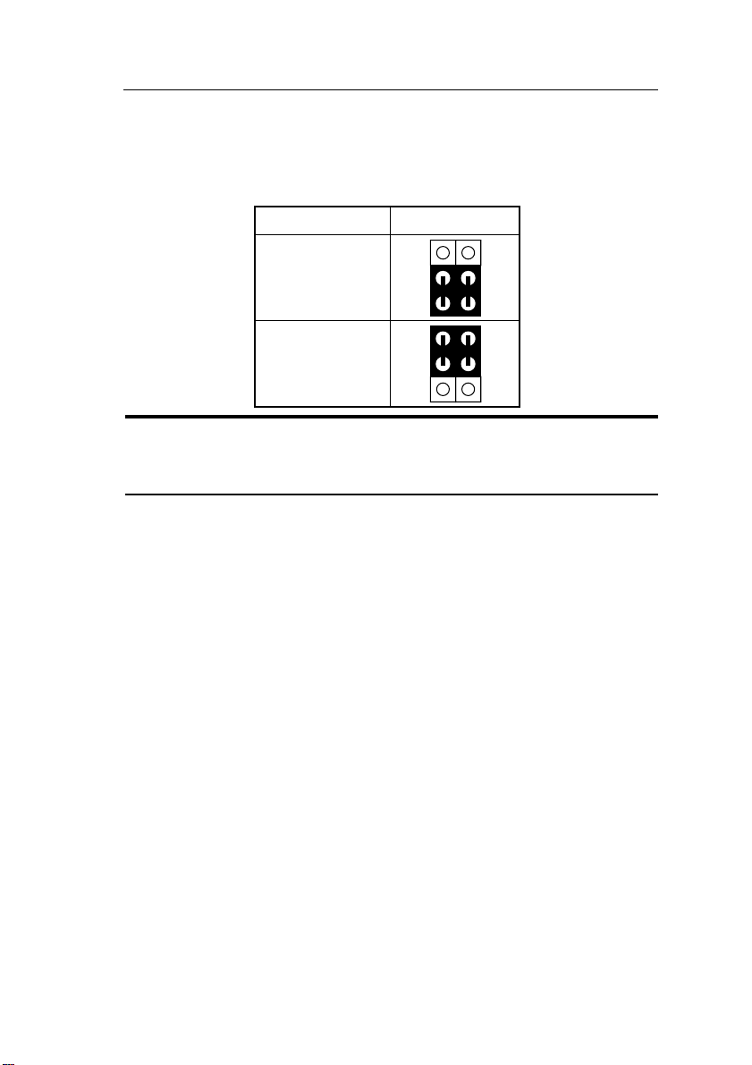
JP37: DIMM Voltage Jumper
There are two kinds of DIMM voltages in the marketÑ3.3V and 5VÑ
and most of SDRAM DIMMS are 3.3V. Choose the correct voltage
according to the DIMM that you are using.
DIMM Voltage JP37 Setting
1
5V
3.3V
(Default)
Caution: Do not change this jumper to 5V setting unless you are
sure that your DIMMs are 5V. The wrong setting may
cause the system malfunction.
3
5
1
3
5
2
4
6
2
4
6
Page 12
8 Hardware Setup
CPU Type Configuration
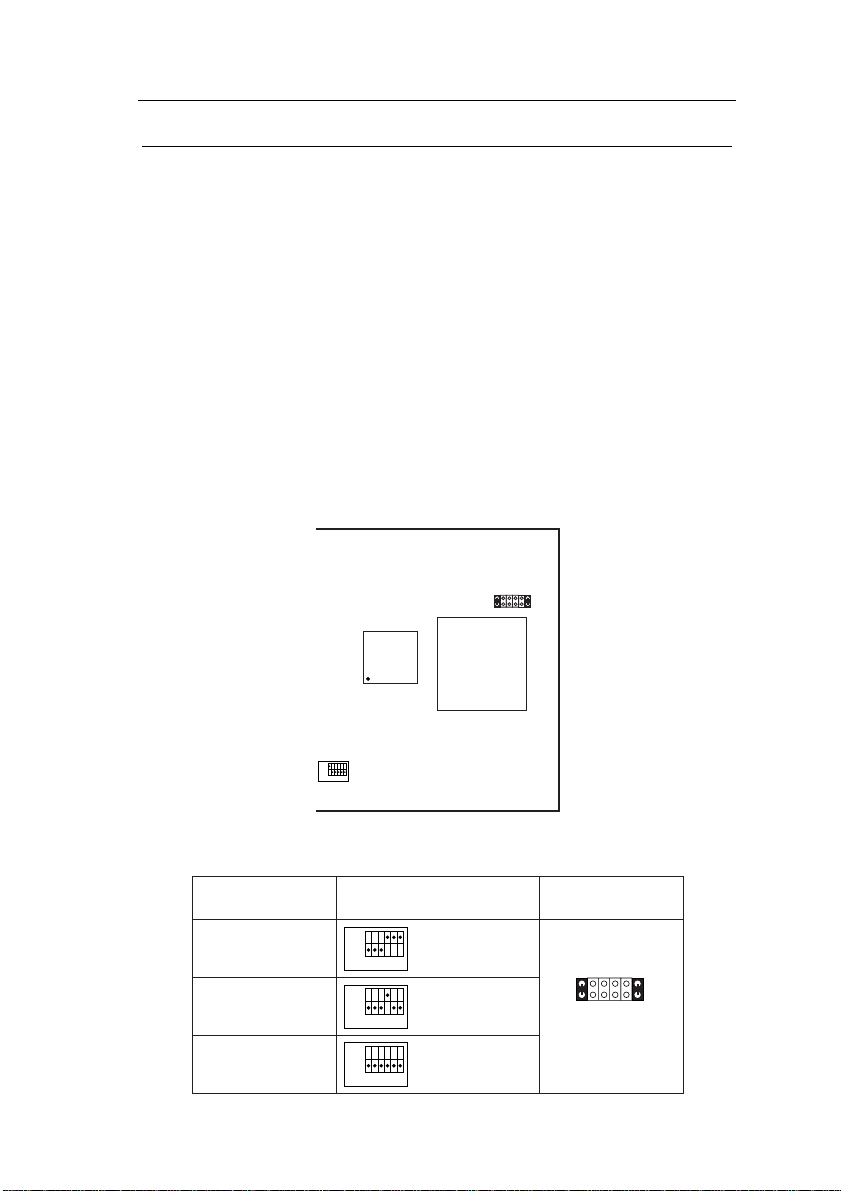
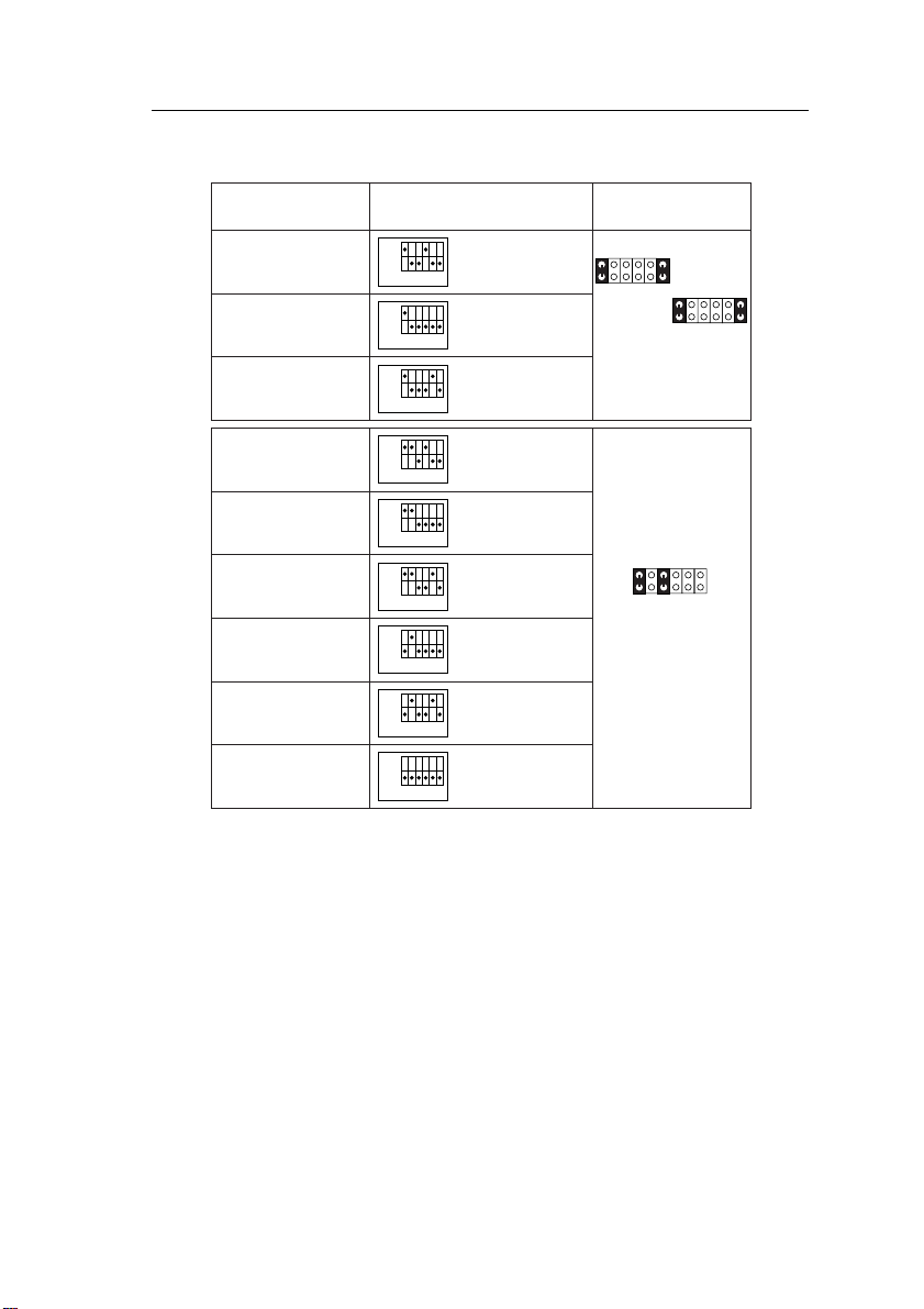
SW1 and JP30 are the only switchs/jumpers that you need to set for your
CPU on this mainboard. Make sure that you know the type of CPU that
you are installing and refer to the proper settings which are listed below.
If you have a higher frequency CPU then the one listed below, see the
ÒQuick Installation GuideÓ for more SW1 information.
SW1: Frequency Setting. Some newer CPUs may not be included in
this section, please refer to the Appendix for more information.
JP30: Voltage Setting. There are two kinds of CPU voltages
currently on the marketÑSingle and Dual. The CPUs which
fall under the single voltage category are: P54C, AMD-K5, and
Cyrix 6x86. The CPUs which fall under the dual voltage
category are: P55C, AMD-K6, and Cyrix 6x86L/MX. This
board is designed to detect the CPU voltage automatically for
P54C and P55C CPUs due to the Smart Detect CPU Voltage
function, and therefore, there is no need to move any jumpers to
set the voltage for P54C/P55C CPUs.
JP30
31
115 7 9
EQ82C6628
ON
123 456
SW1
Figure 2Ð1. Location of JP30 and SW1
P54C/P55C Series CPUs Settings
CPU Frequency Setting (SW1)
P54CÐ75MHz
P54CÐ90MHz
P54CÐ100MHz
ON
ON
ON
External• : 50MHz
Ratio• : 1.5x
123456
External• : 60MHz
Ratio• : 1.5x
123456
External• : 66MHz
Ratio• : 1.5x
123456
Socket 7
(for 586 CPUs)
Voltage Setting
(JP30)
JP30
1357911
Single Voltage
3.52V
(default)
Page 13
Hardware Setup 9
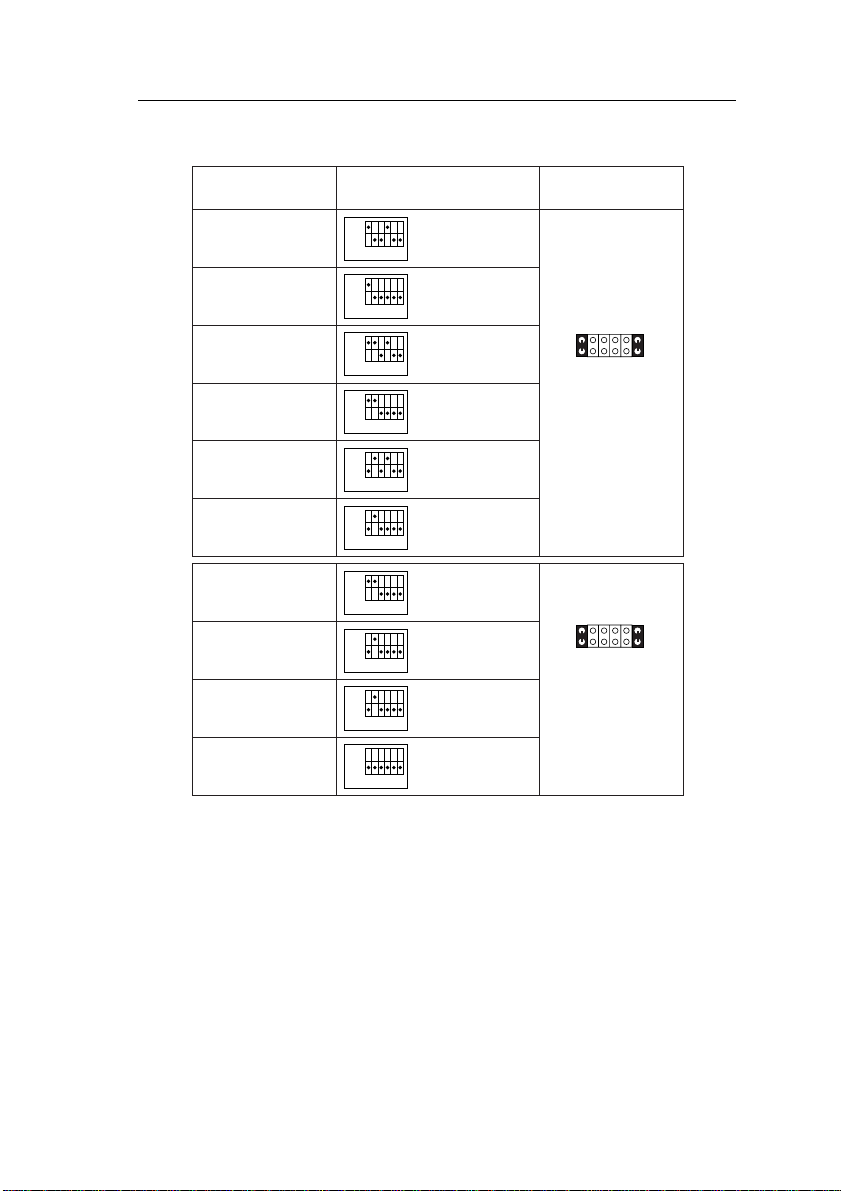
P54C/P55C Series CPUs Settings (Continued)
CPU Frequency Setting (SW1)
P54CÐ120MHz
P54CÐ133MHz
(default)
P54CÐ150MHz
P54CÐ166MHz
P54CÐ180MHz
P54CÐ200MHz
ON
ON
ON
ON
ON
ON
External• : 60MHz
Ratio• : 2.0x
123456
External• : 66MHz
Ratio• : 2.0x
123456
External• : 60MHz
Ratio• : 2.5x
123456
External• : 66MHz
Ratio• : 2.5x
123456
External• : 60MHz
Ratio• : 3.0x
123456
External• : 66MHz
Ratio• : 3.0x
123456
Voltage Setting
(JP30)
JP30
1357911
Single Voltage
3.52V
(default)
P55CÐ166MHz
(MMX)
P55CÐ180MHz
(MMX)
P55CÐ200MHz
(MMX)
P55CÐ233MHz
(MMX)
ON
ON
ON
ON
External• : 66MHz
Ratio• : 2.5x
123456
External• : 60MHz
Ratio• : 3.0x
123456
External• : 66MHz
Ratio• : 3.0x
123456
External• : 66MHz
Ratio• : 3.5x
123456
JP30
11
13579
DualVoltage
2.8V
(default)
Note: The voltage setting for 3.52V and 2.8V are the same due to the
Smart Detect CPU Voltage technology.
Page 14
10 Hardware Setup
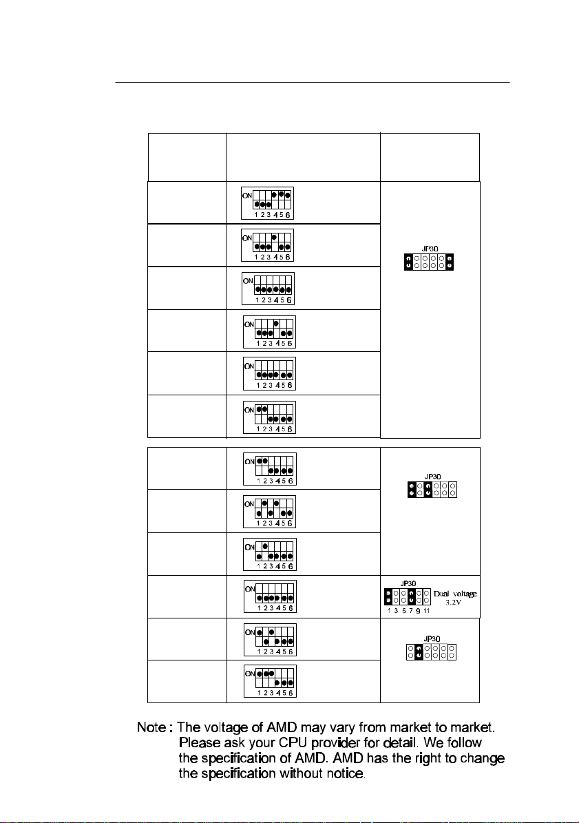
AMD K5/K6 series CPUs setting
CPU
AMD-K5
PR75
AMD-K5
PR90
AMD-K5
PR100
AMD-K5
PR120
AMD-K5
PR133
AMD-K5
PR166
AMD-K6
PR166
AMD-K6
PR180
AMD-K6
PR200
Frequency setting
(SW1)
External : 50MHz
Ratio : 1.5x
External : 60MHz
Ratio : 1.5x
External : 66MHz
Ratio : 1.5x
External: 60MHz
Ratio : 1.5x
External : 66MHz
Ratio : 1.5x
External : 66MHz
Ratio : 2.5x
External: 66MHz
Ratio : 2.5x
External : 60MHz
Ratio : 3.0x
External : 66MHz
Ratio : 3.0x
Voltage setting
(JP30)
1 3 5 7 9 11
Single voltage
3.52V
(default)
1 3
5 7 9 11
Dual voltage
2.9V
AMD-K6
PR233
AMD-K6
PR266
AMD-K6
PR300
External: 66MHz
Ratio : 3.5x
External: 66MHz
Ratio : 4.0x
External: 66MHz
Ratio : 4.5x
1 3
5 7 9 11
Dual voltage
2.2V
Page 15
Hardware Setup 11
Cyrix 6x86/L/MX Series CPUs Setting
CPU Frequency Setting (SW1)
Cyrix 6x86/6x86L
ÐPR150
Cyrix 6x86/6x86L
ÐPR166
Cyrix 6x86/6x86L
ÐPR200
Cyrix 6x86MX
ÐPR166
Cyrix 6x86MX
ÐPR200
Cyrix 6x86MX
ÐPR233
Cyrix 6x86MX
ÐPR233
Cyrix 6x86MX
ÐPR266
Cyrix 6x86MX
ÐPR266
ON
ON
ON
ON
ON
ON
ON
ON
ON
External• : 60MHz
Ratio• : 2.0x
123456
External• : 66MHz
Ratio• : 2.0x
123456
External• : 75MHz
Ratio• : 2.0x
123456
External• : 60MHz
Ratio• : 2.5x
123456
External• : 66MHz
Ratio• : 2.5x
123456
External• : 75MHz
Ratio• : 2.5x
123456
External• : 66MHz
Ratio• : 3.0x
123456
External• : 75MHz
Ratio• : 3.0x
123456
External• : 66MHz
Ratio• : 3.5x
123456
Voltage Setting
(JP30)
JP30
1357911
Single
Voltage
3.52V
(default)
JP30
1357911
Dual
Voltage
2.8V
(default)
JP30
1357911
Dual Voltage
2.9V
Note: 1. There are two kinds of Cyrix MXÐPR233/266 CPUs as you
could see on the above list. Make sure the type of your CPU
first from your CPU provider and then set the SW1 and JP30.
2. The voltage setting for 3.52V and 2.8V are the same due to
the Smart Detect CPU Voltage technology.
Page 16

12 Hardware Setup
Memory Configuration
The mainboard supports one bank of 72-pin 5V FPM/EDO/Burst EDO
DRAM (SIMM), and three strips of 168-pin 3.3V/5V Unbuffered
DIMM modules. The mainboard requires SIMM of at least 70ns access
time.
The mainboard supports SIMM bank and DIMM banks from 4 to 128
MB with no other restrictions on memory configurations. You can install
memory in any combination without having to rely on a memory
configuration table. Memory configuration is thus ÒTable-FreeÓ in any
memory bank. You must install two SIMM modules to complete a bank.
Memory Configuration Table
SIMM Bank DIMM Bank
Bank 0 DIMM 1 DIMM 2 DIMM 3
RAM Type FPM/EDO FPM/BEDO
/SDRAM
Single
RAM
Module
Size (MB)
4/8/16/32/64 4/8/16/32/64
/128
FPM/EDO/
SDRAM
4/8/16/32/64
/128
FPM/EDO/
SDRAM
4/8/16/32/64
/128
Note: Do not install FPM or EDO SIMM/DIMM when you already
installed SDRAM type of DIMM.
RAM Bank Installation Notice
Due to the RAS line share architecture of ETEQ chipset, do not install
SIMM bank with DIMM1. All other combinations are acceptable.
Page 17

Hardware Setup
13
Cache Configuration
The mainboard has a write-back caching scheme with built-in 512KB or
1MB Level 2 Pipelined Burst cache onboard to i mprove th e syst em
performance.
L2 Cache Size and RAM Locations
Cache Size Cache RAM TAG RAM Cacheable
Range
512KB 64k x 64
on U4
16K x 8 on U11
(1 tag)
16K x 8 on U11,U10 (2
tags)
64 MB (1 dirty bit)
128 MB (0 dirty bit) *
256 MB (1 dirty bit) *
512 MB (0 dirty bit) *
1MB 64k x 64
U4, U8
* :1.The performance of 1MB cache is better than 512KB cache even the
cacheable range is the same.
2. You could change the dirty bit from item “Sustained 3T Write” or
“Dirty bit” in “Chipset Feature Setup” sub-menu of BIOS setup
and “Enabled” means dirty bit set to 0, “Disabled” means dirty bit
set to 1.
16K x 8 on U11
(1 tag)
16K x 8 on U11,U10 (2
tags)
128 MB (1 dirty bit) *
256 MB (0 dirty bit) *
512 MB (1 dirty bit) *
512 MB (0 dirty bit) *
Multi I/O Port Addresses
Default settings for multi-I/O port addresses are shown in the table below.
Port I/O Address IRQ Mode
LPT1*
COM1
COM2
If default I/O port a ddresses confl ict with other I/O cards (e.g. sound
car ds or I/O cards), you must adjust on e of the I/O addresses to avoid
address conflict. (You ca n adjust these I/O addresses fr om the BIOS
setup.)
Note: Some sound cards have a default IRQ setting for IRQ7, which may
conflic t with print ing functions. If this occurs do not use sound card
functions at the same time you print.
378H 7 ECP + EPP
3F8H 4
2F8H 3
Page 18

14 Hardware Setup
Connectors
Attach the mainboard to case devices via connectors on the mainboard.
Refer to Figure 1-1 for connector locations and connector pin positions.
Front Panel Connectors
Connector’s
Name
HD LED IDE device LED connector: Attach a 2-pin IDE drive
LED cable to this connector. The LED lights when an
IDE device is active.
KB_LOCK Keylock & Power LED connector: It is a 5-pin
connector for a lock that may be installed on the system
case for enabling or disabling the keyboard. It also
attaches to the caseÕs Power LED. Pin 1, 3 are for power
LED and pin 4, 5 are for keylock.
PW2 ATX power on/off switch connector: Attach a 2-pin
momentary type switch to this connector for turning on
or off your ATX power supply.
RESET Hardware reset switch connector: Attach 2-pin hardware
reset switch to it. Closing the reset switch restarts the
system.
SPEAK PC speaker connector: Attach a 4-pin PC speaker cable
from the case to this connector.
TB LED Turbo LED connector: Attach a 2-pin turbo LED cable
to it. The LED lights when the system is in turbo mode.
Manufacture default has set the board in turbo mode due
to most of hardware and software are compliance to
turbo mode.
Description
Page 19
Hardware Setup 15
Back Panel Connectors
Connector’s
Name
COM1/
COM2
PS/2
Keyboard
Connector
COM1/COM2 serial port connectors: Attach
COM1/COM2 device cables to these connectors.
PS/2 keyboard port connector: A 6-pin female PS/2
keyboard connector is located at the rear of the board.
Plug the PS/2 keyboard jack into this connector.
PRT Parallel port connector: A 26-pin female connector is
located at the rear of the board. Plug the parallel port
device cable into this connector.
USB1/2 USB ports connectors: Two female connector is located
at the rear of the board. Plug the USB devices jack into
this connector.
Description
Other Connectors
Connector’s
Name
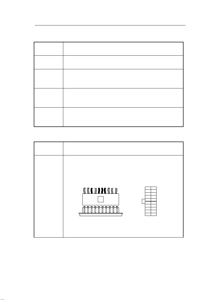
ATX PW ATX power supply connector: It is a twenty-pin male
header connector. Plug the connector from the power
directly onto the board connector while making sure the
pin1 is in its position. The mainboard requires a power
supply with at least 200 watts and a Òpower goodÓ signal.
Description
PS-ON
3.3V
–12V
GND
GND
GND
GND
–5V
3.3V
3.3V
GND
5V
GND
5V
GND
PW-0K
5V
5V
5VSB
12V
Note: Make sure that the ATX power supply can take
at least 10mAmp load on the 5V StanBy lead
(5VSB) to meet the standard ATX specification.
Page 20
16 Hardware Setup
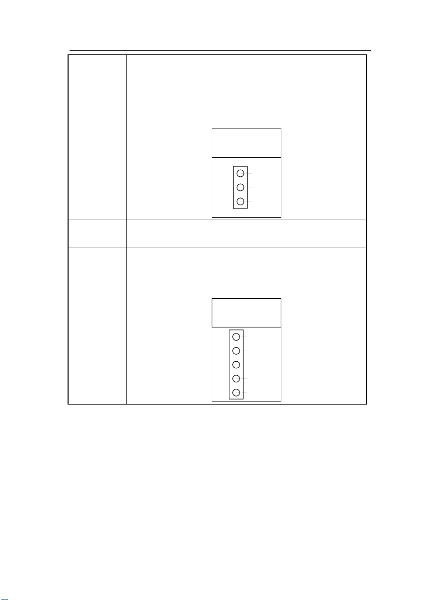
Fan (JP43) CPU cooling fan connector: Attach a 3-pin CPU cooling
fan cable to this connector. Make sure the pin
assignment of the fan matches this connector or you may
damage the system. This fan will stop when the system
is into the suspend mode, if you enable the Suspend
Mode in the BIOS setup.
CPU Cooling Fan
Pin Assignment
GND
1
12V
2
Empty
3
IDE1/IDE2 Primary/Secondary IDE device connectors: Attach the
IDE device cables to these connectors.
IR Infrared device connector: Attach a 5-pin infrared device
cable to this connector for enabling the infrared transfer
function. This mainboard meets the specification of
ASKIAR and HPSIR.
IR Connector
Pin Assignment
VCC
1
Empty
2
IRRX
3
GND
4
IRTX
5
Page 21
Hardware Setup 17
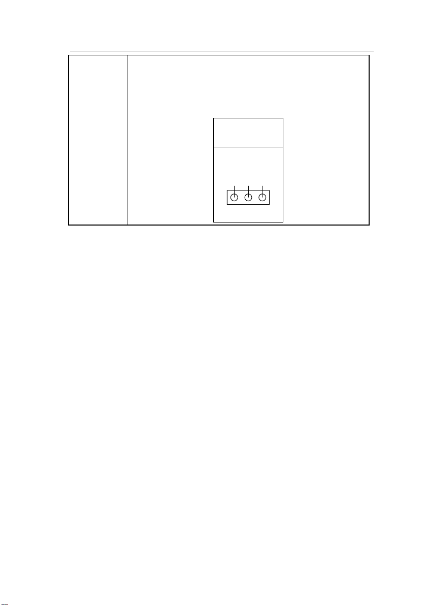
JP44 Wake-on-LAN connector: Attach a 3-pin connector
from the LAN card which supports the Wake-On-LAN
(WOL) function. This function lets users wake up the
connected computer through the LAN card. (The cable
should be included with the LAN card.)
Wake-on-LAN
Pin Assignment
5V
GND
SENSOR
123
Page 22

3 BIOS Setup
The mainboardÕs BIOS setup program is the ROM PCI/ISA BIOS from
Award Software Inc. Enter the Award BIOS programÕs Main Menu as
follows:
1. Turn on or reboot the system. After a series of diagnostic checks,
you are asked to press DEL to enter Setup.
2. Press the <DEL> key to enter the Award BIOS program and the
main screen appears:
STANDARD CMOS SETUP
BIOS FEATURES SETUP
CHIPSET FEATURES SETUP
POWER MANAGEMENT SETUP
PNP/PCI CONFIGURATION
LOAD SETUP DEFAULTS
LOAD BIOS DEFAULTS
Esc : Quit ↑ ↓ → ← : Select Item
F10 : Save & Exit Setup (Shift) F2 : Change Color
3. Choose an option and press <Enter>. Modify the system parameters
to reflect the options installed in the system. (See the following
sections.)
4. Press <ESC> at anytime to return to the Main Menu.
5. In the Main Menu, choose ÒSAVE AND EXIT SETUPÓ to save
your changes and reboot the system. Choosing ÒEXIT WITHOUT
SAVINGÓ ignores your changes and exits the program.
ROM PCI/ISA BIOS
CMOS SETUP UTILITY
AWARD SOFTWARE, INC.
INTEGRATED PERIPHERALS
SUPERVISOR PASSWORD
USER PASSWORD
IDE HDD AUTO DETECTION
SAVE & EXIT SETUP
EXIT WITHOUT SAVING
Time, Date, Hard Disk Type...
The Main Menu options of the Award BIOS are described in the sections
that follow.
Page 23

BIOS Setup 19
Standard CMOS Setup
Run the Standard CMOS Setup as follows.
1. Choose ÒSTANDARD CMOS SETUPÓ from the Main Menu. A
screen appears.
Date (mm:dd:yy) : Fri, Feb 1 1995
Time (hh:mm:ss) : 7 : 30 : 33
HARD DISKS TYPE SIZE CYLS HEAD PRECOMP LANDZ SECTOR MODE
Primary Master : AUTO 0 0 0 0 0 0 AUTO
Primary Slave : None 0 0 0 0 0 0 ---Secondary Master : None 0 0 0 0 0 0 ---Secondary Slave : None 0 0 0 0 0 0 ----
Drive A : 1.44M, 3.5 in.
Drive B : None
Floppy 3 Mode Support : Disabled
Video : EGA/VGA
Halt On : All Errors
Esc : Quit ↑ ↓ → ← : Select Item PU/PD/+/– : Modify
F11 : Help (Shift) F2 : Change Color F3 : Toggle Calendar
2. Use arrow keys to move between items and select values. Modify
selected fields using PgUp/PgDn/+/Ð keys. Some fields let you enter
values directly.
Date (mm/dd/yy) Type the current date.
ROM PCI/ISA BIOS
STANDARD CMOS SETUP
AWARD SOFTWARE, INC.
Extended Memory: 3328K
Base Memory: 640K
Other Memory: 128K
Total Memory: 4096K
Time (hh:mm:ss) Type the current time.
Primary
(Secondary)
Master & Slave
First, choose the type of hard disk that you
already installed:
Auto Ð BIOS detects hard disk type
automatically (default)
1 ~ 46 Ð Selects standard hard disk type
User Ð User defines the type of hard disk.
Next, choose hard disk mode:
Auto Ð BIOS detects hard disk mode
automatically (default)
Normal Ð Normal IDE hard disk (smaller than
528MB)
LBA Ð EnhancedÐIDE hard disk (larger
than 528MB)
Page 24

20 BIOS Setup
Primary
(Secondary)
Master & Slave
(Continued)
Drive A & B Choose 360KB , 5 1/4 in.,
Floppy 3 Mode
Support
Video Choose Monochrome, Color 40x25,
Halt On When BIOS detects system errors, this function
Large Ð Large IDE hard disk (for certain
hard disk)
Note: If you have any questions on your hard
disk type or mode, ask your hard disk
provider or previous user for details.
1.2MB , 5 1/4 in.,
720KB , 3 1/2 in.,
1.44M , 3 1/2 in.(default),
2.88 MB, 3 1/2 in. or
Not installed
Choose Disabled (default) or Enabled. When
enables this function, the system will support
720KB/1.25MB/1.44MB 3 different modes
floppy diskette.
Note: This function is for a special disk drive
which happens to be popular in Japan.
VGA/EGA (default), Color 80x25
will stop the system. Choose one of the
following options to make system halt.
All Errors (default) All, But Diskette
No Errors All, But Keyboard
All, But Disk/Key
3. When you finish, press the <ESC> key to return to the Main Menu.
Page 25

BIOS Setup 21
BIOS Features Setup
Run the BIOS Features Setup as follows.
1. Choose ÒBIOS FEATURES SETUPÓ from the Main Menu and a
screen with a list of items appears. (The screen below shows the
BIOS default settings.)
CPU Internal Cache : Enabled
External Cache : Enabled
Quick Power on Self Test : Enabled
Boot Sequence : A,C,SCSI
Swap Floppy Drive : Disabled
Boot Up NumLock Status : On
Typematic Rate Setting : Disabled
Typematic Rate (Chars/Sec) : 6
Typematic Delay (Msec) : 250
Security Option : Setup
IDE Second Channel Control : Enabled
PS/2 Mouse Function Control: Disabled
PCI/VGA Palette Snoop : Disabled
OS Select for DRAM >64MB : Non-OS2
2. Use the arrow keys to move between items and to select values.
Modify the selected fields using the PgUp/PgDn/+/Ð keys. <F> keys
are explained below:
<F1>: ÒHelpÓ gives options available for each item.
Shift <F2>: Change color.
<F5>: Get the old values. These values are the values with
which the user started the current session.
<F6>: Load all options with the BIOS Setup default values.
<F7>: Load all options with the Power-On default values.
ROM PCI/ISA BIOS
BIOS FEATURES SETUP
AWARD SOFTWARE, INC.
Video BIOS Shadow : Enabled
C8000-CBFFF Shadow : Disabled
CC000-CFFFF Shadow : Disabled
D0000-D3FFF Shadow : Disabled
D4000-D7FFF Shadow : Disabled
D8000-DBFFF Shadow : Disabled
DC000-DFFFF Shadow : Disabled
ESC : Quit ↑ ↓ → ←: Select Item
F1 : Help PU/PD/+/– : Modify
F5 : Old Values (Shift)F2 : Color
F6 : Load BIOS Defaults
F7 : Load Setup Defaults
A short description of screen items follows:
CPU Internal
Cache
This option enables/disables the CPUÕs internal
cache. (The Default setting is Enabled.)
External Cache This option enables/disables the external cache
memory. (The Default setting is Enabled.)
Quick Power
Enabled provides a fast POST at boot-up .
On Self Test
Page 26

22 BIOS Setup
Boot Sequence Choose the boot device sequence as your need. For
example, ÒA, C, SCSIÓ means BIOS will look for an
operating system first from drive A, drive C, then
SCSI device. Options of this function are:
A, C, SCSI
C, A, SCSI
C, CDÐROM, A
CDÐROM, C, A
D, A, SCSI
E, A, SCSI
F, A, SCSI
SCSI, A, C
SCSI, C, A
C only.
Swap Floppy
Drive
Boot Up Num
Lock Status
Typematic Rate
Setting
Typematic Rate
(Chars/Sec)
Typematic
Delay (Msec)
Security Option Choose Setup or System. Use this feature to prevent
Enabled changes the sequence of the A: and B:
drives. (The Default setting is Disabled.)
Choose On or Off. On puts numeric keypad in Num
Lock mode at boot-up. Off puts this keypad in arrow
key mode at boot-up.
Enable this option to adjust the keystroke repeat rate.
Choose the rate a character keeps repeating.
Choose how long after you press a key that a
character begins repeating.
unauthorized system boot-up or use of BIOS Setup.
ÒSystemÓ Ð Each time the system is booted the
password prompt appears.
ÒSetupÓÐ If a password is set, the password prompt
only appears if you attempt to enter the Setup
program.
Page 27

BIOS Setup 23
IDE Second
Channel
Control
PS/2 Mouse
Function
Control
PCI/VGA
Palette Snoop
OS Select for
DRAM >64MB
Video or
Adapter BIOS
Shadow
3. After you have finished with the BIOS Features Setup program,
press the <ESC> key and follow the screen instructions to save or
disregard your settings.
Default setting is Enabled. Choose Disabled when
you need to turn off the onboard IDE second
channel.
Default setting is Disabled. You need to enable this
function when the PS/2 mouse is attached.
Enabled: The color of the monitor may be incorrect
if uses with MPEG card. Enable this
option to make the monitor normal.
Disabled: Default setting.
OS2 Ð Choosing this when you are using OS/2
operation system.
Non-OS/2 Ð Choosing this when you are using no-
OS/2 operation system.
BIOS shadow copies BIOS code from slower ROM
to faster RAM. BIOS can then execute from RAM.
These 16K segments can be shadowed from ROM to
RAM. BIOS is shadowed in a 16K segment if it is
enabled and it has BIOS present.
Page 28

24 BIOS Setup
Chipset Features Setup
The Chipset Features Setup option changes the values of the chipset
registers. These registers control system options in the computer.
Note: Change these settings only if you are familiar with the Chipset.
Run the Chipset Features Setup as follows.
1. Choose ÒCHIPSET FEATURES SETUPÓ from the Main Menu and
the following screen appears. (The screen below shows default
settings.)
ROM PCI/ISA BIOS
CHIPSET FEATURES SETUP
AWARD SOFTWARE, INC.
Bank 0/1 DRAM Timing : 60ns
Read Pipeline : Disabled
Write Pipeline : Enabled
Video BIOS Cacheable : Disabled
System BIOS Cacheable : Disabled
Memory hole At 15Mb Addr. : Disabled
OnChip USB : Disabled
ESC : Quit ↑ ↓ → ←: Select Item
F1 : Help PU/PD/+/– : Modify
F5 : Old Values (Shift)F2 : Color
F6 : Load BIOS Defaults
F7 : Load Setup Defaults
2. Use the arrow keys to move between items and select values.
Modify selected fields using the PgUp/PgDn/+/Ð keys.
A short description of screen items follows:
Bank 0/1 DRAM Timing Choose 60ns, 70ns, Normal, Medium,
Fast, or Turbo. Normal is the slowest and
you must check the system stability before
you change to the Fast of Turbo setting.
Choose 60ns or 70ns only when you know
the exact timing of the DRAM.
DRAM Read Pipeline Use the default setting.
Cache Rd + CPU Wt
Use the default setting.
Pipeline
Read Around Write Use the default setting.
Page 29

BIOS Setup 25
Linear Burst Choose Enabled when you installed a
Cyrix CPU and set JP22 to Linear mode.
Video BIOS Cacheable Disabled Ð The ROM area F0000H-
FFFFFH is not cached.
Enabled Ð The ROM area F0000H-
FFFFFH is cacheable if cache
controller is enabled.
System BIOS Cacheable Disabled Ð The video BIOS C0000H-
C7FFFH is not cached.
Enabled Ð The video BIOS C0000H-
C7FFFH is cacheable if cache
controller is enabled.
Memory Hole At 15Mb
Addr
AGP Choose Enabled when you wish to use
AGP Aperture Size AGP could use the DRAM as its video
OnChip USB Default is Disabled. Enable this function
USB Keyboard Support Enable this function when you use the
Choose Enabled or Disabled (default).
Some interface cards will map their ROM
address to this area. If this occurs, you
should select Enabled, otherwise use
Disabled.
DRAM to extend the size of your AGP
VGA cardÕs VRAM.
RAM. Choose the DRAM size that you
want it to be used as video RAM. The
range is from 4MB to 256MB.
when you use the USB device.
USB keyboard, but notice that you need to
use the regular keyboard first before
getting in the BIOS setup.
Page 30

26 BIOS Setup
Spread Spectrum
Modulated
3. After you have finished with the Chipset Features Setup, press the
<ESC> key and follow the screen instructions to save or disregard
your settings.
Choose Disabled (default) or Enabled.
Select Enabled when uses Spread
Spectrum Modulated 1.5% or 6% for FCC
or DOC testing.
Page 31

BIOS Setup 27
Power Management Setup
The Power Management Setup option sets the systemÕs power saving
functions.
Run the Power Management Setup as follows.
1. Choose ÒPOWER MANAGEMENT SETUPÓ from the Main Menu
and a screen with a list of items appears.
Power Management : Disabled
PM Control by APM : Yes
Video Off Option : Suspend -> Off
Video Off Method : V/H SYNC+Blank
Conserve Mode : Disabled
** PM Timers **
HDD Power Down : Disabled
Doze Mode : Disabled
Suspend Mode : Disabled
** PM Events **
VGA : OFF
LPT & COM : LPT/COM
HDD & FDD : ON
DMA/master : OFF
Primary INTR : ON
IRQ 3 (COM 2) : Primary
IRQ 4 (COM 1) : Primary
2. Use the arrow keys to move between items and to select values.
Modify the selected fields using the PgUp/PgDn/+/- keys.
ROM PCI/ISA BIOS
CMOS SETUP UTILITY
POWER MANAGEMENT SETUP
** Power Down & Resume Events **
IRQ 5 (LPT 2) : Primary
IRQ 6 (Floppy Disk) : Primary
IRQ 7 (LPT 1) : Primary
IRQ 8 (RTC Alarm) : Disabled
IRQ 9 (IRQ2 Redir) : Secondary
IRQ 10 (Reserved) : Secondary
IRQ 11 (Reserved) : Secondary
IRQ 12 (PS/2 mouse) : Primary
IRQ 13 (Coprocessor) : Primary
IRQ 14 (Hard Disk) : Primary
IRQ 15 (Reserved) : Disabled
ESC : Quit ↑ ↓ → ←: Select Item
F1 : Help PU/PD/+/– : Modify
F5 : Old Values (Shift)F2 : Color
F6 : Load BIOS Defaults
F7 : Load Setup Defaults
A short description of selected screen items follows:
Power
Management
Options are as follows:
User Define Ð LetÕs you define the HDD and
system power down times.
Disabled Ð Disables the Green PC Features.
Min Saving Ð Doze timer = 1 Hour
Suspend timer = 1 Hour
HDD Power Down = 15 Min
Max Saving Ð Doze timer = 10 Sec
Suspend timer = 10 Sec
HDD Power Down = 1 Min
Page 32

28 BIOS Setup
PM Control by
APM
Video Off Option Susp, Stby→off:Video off when the system
Video Off Method Choose V/H Sync+Blank (default), Blank
Conserve Mode Use the default setting.
HDD Power Down When the set time has elapsed, the BIOS sends a
Choose Yes (default) or No. APM stands for
Advanced Power Management. To use APM,
you must run Òpower.exeÓ under DOS v6.0 or
later version.
runs into Suspend or Standby
mode.
All Modes→off: Video off in all modes.
Always On: Video never off.
Suspend→off: Video off when system runs
into the suspend mode.
screen, or DPMS for the selected PM mode.
command to the HDD to power down, which
turns off the motor. Time is adjustable from 1 to
15 minutes. The default setting is Disabled.
Some older model HDDs may not support this
advanced function.
Doze Mode When the set time has elapsed, the BIOS sends a
command to the system to enter doze mode
(system clock drops to 33MHz). Time is
adjustable from 10 seconds to 1 Hour.
Suspend Mode The default is Disabled. Only an SL-Enhanced
(or SMI) CPU can enter this mode. Time is
adjustable from 10 seconds to 1 Hour. Under
Suspend mode, the CPU stops completely (no
instructions are executed.)
VGA Choose Off (default) or On to disable or enable
the power management.
Page 33

BIOS Setup 29
LPT & COM Choose LPT/COM (default) or LPT (COM) to
enable the power management timer. Choose
NONE to disable the power management timer.
HDD &FDD Choose On (default) to enable the power
management timer, or Off to disable the power
management timer.
DMA/master Choose Off (default) or On. If you choose the
system ÒOffÓ, will not monitor the signal of
DMA/master; and when you choose ÒOnÓ, the
system will not have SMI signal until the master
is finished while the master is working.
Primary INTR When On (default) is chosen, you can choose
any IRQ #.
IRQ# When set at ÒPrimaryÓ the processor will power
down only after the BIOS detects a Òno IRQ
activityÓ during the time specified by the
Suspend time. If set at ÒSecondary eventÓ the
system will distinguish whether an interrupt
accesses and I/O address or not. If it does, the
system enters the standby mode. If not, the
system enters the dreaming mode; that is the
system goes back full-on status but leaves the
monitor blank. For instance, if the system
connects to a LAN and receives an interrupt
from its file server, the system will enter the
dreaming mode to execute the corresponding
calling routine.
3. After you have finished with the Power Management Setup, press
the <ESC> key to return to the Main Menu.
Page 34

30 BIOS Setup
PNP/PCI Configuration Setup
This option sets the mainboardÕs PCI Slots. Run this option as follows:
1. Choose ÒPNP/PCI CONFIGURATION SETUPÓ from the Main
Menu and the following screen appears. (The screen below shows
default settings.)
ROM PCI/ISA BIOS
PNP/PCI CONFIGURATION
AWARD SOFTWARE, INC.
Resources Controlled By : Manual
Reset Configuration Data : Disabled
IRQ-3 assigned to : Legacy ISA*
IRQ-4 assigned to : Legacy ISA*
IRQ-5 assigned to : PCI/ISA PnP*
IRQ-7 assigned to : PCI/ISA PnP*
IRQ-9 assigned to : PCI/ISA PnP*
IRQ-10 assigned to : PCI/ISA PnP*
IRQ-11 assigned to : PCI/ISA PnP*
IRQ-12 assigned to : PCI/ISA PnP*
IRQ-14 assigned to : PCI/ISA PnP*
IRQ-15 assigned to : PCI/ISA PnP*
DMA-0 assigned to : PCI/ISA PnP*
DMA-1 assigned to : PCI/ISA PnP*
DMA-3 assigned to : PCI/ISA PnP*
DMA-5 assigned to : PCI/ISA PnP*
DMA-6 assigned to : PCI/ISA PnP*
DMA-7 assigned to : PCI/ISA PnP*
*: These items will disappear when Resource Controlled. is Auto.
PCI IRQ Actived By : Level
PCI IDE IRQ Map To : PCI-AUTO
Primary IDE INT# : A
Secondary IDE INT# : B
ESC : Quit ↑ ↓ → ←: Select Item
F1 : Help PU/PD/+/– : Modify
F5 : Old Values (Shift)F2 : Color
F6 : Load BIOS Defaults
F7 : Load Setup Defaults
2. Use the arrow keys to move between items and select values.
Modify selected fields using the PgUp/PgDn/+/Ð keys.
A short description of screen items follows:
Resources
Controlled By
Manual Ð BIOS doesnÕt manage PCI/ISA PnP
card (i.e., IRQ) automatically.
Auto Ð BIOS auto manage PCI and ISA PnP
card (recommended).
Reset
Configuration
Disabled Ð Retain PnP configuration data in
BIOS.
Data
Enabled Ð Reset PnP configuration data in
BIOS.
Page 35

BIOS Setup 31
IRQX and
DMAX assigned
to
PCI IRQ
Activated By
PCI IDE IRQ
Map To
Primary IDE
INT#
Secondary IDE
INT#
3. After you have finished with the PCI Slot Configuration, press the
<ESC> key and follow the screen instructions to save or disregard
your settings.
Choose PCI/ISA PnP or Legacy ISA. If the first
item is set to Manual, you could choose IRQX
and DMAX assigned to PCI/ISA PnP card or ISA
card.
Choose Edge or Level. Most PCI trigger signals
are Level. This setting must match the PCI card.
Select PCI-AUTO, ISA, or assign a PCI SLOT
number (depending on which slot the PCI IDE is
inserted). The default setting is PCI-AUTO. If
PCI-AUTO does not work, then assign an
individual PCI SLOT number.
Choose INTA#, INTB#, INTC#, or INTD#. The
default setting is INTA#.
Choose INTA#, INTB#, INTC#, or INTD#. The
default setting is INTB#.
Page 36

32 BIOS Setup
Load Setup Defaults
This item loads the system values you have previously saved. Choose
this item and the following message appears:
ÒLoad SETUP Defaults (Y/N)? NÓ
To use the SETUP defaults, change the prompt to ÒYÓ and press
<Enter>. This item is recommended if you need to reset the system
setup.
Note: The SETUP Defaults are optimized for the most stabilized
performance.
Load BIOS Defaults
Choose this item and the following message appears:
ÒLoad BIOS Defaults (Y/N)?NÓ
To use the BIOS defaults, change the prompt to ÒYÓ and press <Enter>.
Note: BIOS DEFAULTS values are adjusted for high performance. If
you run into any problems after loading BIOS DEFAULTS,
please load the SETUP DEFAULTS for the stable performance.
Page 37

BIOS Setup 33
Integrated Peripherals
The Integrated Peripherals option changes the values of the chipset
registers. These registers control system options in the computer.
Note: Change these settings only if you are familiar with the Chipset.
Run the Integrated Peripherals as follows.
1. Choose ÒIntegrated PeripheralsÓ from the Main Menu and the
following screen appears. (The screen below shows default
settings:)
OnChip IDE First Channel : Enabled
OnChip IDE Second Channel: Enabled
IDE Prefetch Mode : Enabled
IDE HDD Block Mode : Enabled
IDE Primary Master PIO : Auto
IDE Primary Slave PIO : Auto
IDE Secondary Master PIO : Auto
IDE Secondary Slave PIO : Auto
IDE Secondary Master UDMA: Auto
IDE Secondary Slave UDMA: Auto
Onboard FDC Controller : Enabled
Onboard UART 1 : 3F8/IRQ4
Onboard UART 2 : 2F8/IRQ3
Onboard UART 2 Mode : Standard
Onbaord Parallel Port : 378/IRQ7
Parallel Port Mode : ECP+EPP
ECP Mode Use DMA : 3
Parallel Port EPP Type : EPP1.9
ROM PCI/ISA BIOS
INTEGRATED PERIPHERALS
AWARD SOFTWARE, INC.
ESC : Quit ↑ ↓ → ←: Select Item
F1 : Help PU/PD/+/– : Modify
F5 : Old Values (Shift)F2 : Color
F6 : Load BIOS Defaults
F7 : Load Setup Defaults
2. Use the arrow keys to move between items and select values.
Modify selected fields using the PgUp/PgDn/+/Ð keys.
A short description of screen items follows:
On-chip IDE First
Channel/
On-chip IDE Second
Enabled Ð Use the on-board IDE
(default)
Disabled Ð Turn off the on-board IDE
Channel
IDE Prefetch Mode Use the default setting.
IDE HDD Block Mode Choose Enabled (default) or Disabled.
Enabled invokes multi-sector transfer
instead of one sector per transfer. Not all
HDDs support this function.
Page 38

34 BIOS Setup
IDE Primary Master PIO/
IDE Primary Slave PIO/
IDE Secondary Master
PIO/
IDE Secondary Slave PIO
IDE Secondary Master
UDMA
IDE Secondary Slave
UDMA
Onboard FDC Controller Enabled Ð Use the on-board floppy
Onboard UART 1/
Onboard UART 2
Onboard UART 2 Mode Standard Ð (default) supports a serial
Choose Auto (default) or mode 0~4.
Mode 0 is the slowest speed, and HDD
mode 4 is the fastest speed. For better
performance and stability, we suggest
you use the Auto setting to set the HDD
control timing.
Choose Auto (defautl) or Disabled.
When Auto is selected, it supports Ultra
DMA Mode.
controller (default).
Disabled Ð Turn off the on-board
floppy controller.
Choose serial port 1 & 2Õs I/O address.
Do no set port 1 & 2 to the same value
except for Disabled.
COM 1/3F8H | COM3/3E8H
COM 2/2F8H | COM4/2E8H
(default)
infrared IrDA.
HPSIR Ð supports HP serial infrared
interface format
ASKIR Ð supports a Sharp serial
interface format.
IR Duplex Mode Use the default setting (Half). This
function shows up only when either
HPSIR or ASKIR is chosen in the
previous function (Onboard UART 2
Mode).
Onboard Parallel Port Choose the printer I/O address:
378H/IRQ7 (default), 3BCH/IRQ7,
278H/IRQ5
Page 39

BIOS Setup 35
Parallel Port Mode Choose ECP + EPP (default), Normal
or EPP, ECP mode. The mode depends
on your external device that connects to
this port.
ECP Mode Use DMA Choose DMA3 (default) or DMA1.
This setting only works when the
Onboard Printer Mode is set at the ECP
mode.
Parallel Port EPP Type Choose EPP specification Ver. 1.7 or 1.9
(default).
Supervisor Password
Based on the setting you made in the ÒSecurity OptionÓ of the ÒBIOS
FEATURES SETUPÓ, this Main Menu item lets you configure the
system so that a password is required every time the system boots or an
attempt is made to enter the Setup program. Change the password as
follows:
1. Choose ÒSUPERVISOR PASSWORDÓ in the Main Menu and press
<Enter>. The following message appears:
ÒEnter Password:Ó
2. Enter a password and press <Enter>.
(If you do not wish to use the password function, you can just press
<Enter> and a ÒPassword disabledÓ message appears. )
3. After you enter your password, the following message appears
prompting you to confirm the new password:
ÒConfirm Password:Ó
4. Re-enter your password and then Press <ESC> to exit to the Main
Menu.
Important: If you forget or lose the password, the only way to access
the system is to set jumper JP5 to clear the CMOS RAM.
All setup information is lost and you must run the BIOS
setup program again.
Page 40

36 BIOS Setup
User Password
Based on the setting you made in the ÒSecurity OptionÓ of the ÒBIOS
FEATURES SETUPÓ, this Main Menu item lets you configure the
system so that a password is required every time the system boots or an
attempt is made to enter the Setup program. Change the password as
follows:
1. Choose ÒUSER PASSWORDÓ in the Main Menu and press <Enter>.
The following message appears:
ÒEnter Password:Ó
2. Enter a password and press <Enter>.
(If you do not wish to use the password function, you can just press
<Enter> and a ÒPassword disabledÓ message appears. )
3. After you enter your password, the following message appears
prompting you to confirm the new password:
ÒConfirm Password:Ó
4. Re-enter your password and then Press <ESC> to exit to the Main
Menu.
5. You are not allowed to change any setting in ÒCMOS SETUP
UTILITYÓ except change userÕs password.
Important: If you forget or lose the password, the only way to access
the system is to set jumper JP5 to clear the CMOS RAM.
All setup information is lost and you must run the BIOS
setup program again.
Page 41

BIOS Setup 37
IDE HDD Auto Detection
This Main Menu item automatically detects the hard disk type and
configures the STANDARD CMOS SETUP accordingly.
Note: This function is only valid for IDE hard disks.
HARD DISKS TYPE SIZE CYLS HEAD PRECOMP LANDZ SECTOR MODE
Primary Master : None 0 0 0 0 0 0 ----
Primary Slave : None 0 0 0 0 0 0 ---Secondary Master : None 0 0 0 0 0 0 ---Secondary Slave : None 0 0 0 0 0 0 ----
ROM PCI/ISA BIOS
CMOS SETUP UTILITY
AWARD SOFTWARE, INC.
Do you accept this drive C (Y/N)? N
ESC : Skip
Page 42
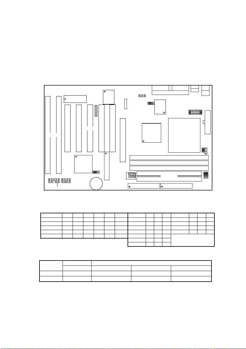
Quick Installation Guide
This Quick Installation Guide leaflet is designed for those people who
are familiar with motherboard settings to set up this new motherboard in
order to boot up the system. Refer back to the proper chapters if you
have run in to any problems.
Motherboard Layout
COM2 COM1
Flash BIOS
SMC8669
IR1
1
5
TAG SRAM
JP44
123
JP22
123
P.B. SRAM
32k x 32
(Slave)
ISA Slot
#2 #1
KB_LOCK
+–
RESET
PW2
PCI Slot
#5 #4 #3 #2 #1
SPEAK
++––
HDD
LEDTBLED
EQ82C6629
JP5
123
3V
Lithium
Battery
FDC
AGP Port
EQ82C6628
DIMM Bank 1 (Share with SIMM Bank)
DIMM Bank 2
DIMM Bank 3
ON
12 345 6
SW1
SIMM Bank
CPU Voltage and Frequency Jumper Settings
Voltage Settings: JP30
Single 3.52V close open open open open close
Single 3.3V close open open open close open
Dual 3.2V close open open close open open
Dual 2.9V close open close open open open
Dual 2.8V close open open open open close
1-2 3-4 5-6 7-8 9-10 11-12
CPU Frequency Settings: SW1
Multiplier 1 2 3 Frequency 4 5 6
1.5x/3.5x off off off 50MHz on on off
2.0x on off off 60MHz off off off
2.5x on on off 66MHz on off off
3.0x off on off 75MHz off on off
4.0x on off on
4.5x on on on
5.0x off on on
PRT
Socket 7
(for 586 CPUs)
IDE2IDE1
USB1
USB2
JP30
31
PS/2 KB
Conn.
PS/2 Mouse
Conn.
115 7 9
JP1
1
JP37
ATX PW
JP43
1
2
3
2
4
6
Memory Configuration
SIMM Bank DIMM Bank
RAM Type FPM/EDO FPM/EDO/SDRAM FPM/EDO/SDRAM FPM/EDO/SDRAM
Size (MB) 4/8/16/32/64 4/8/16/32/64/128 4/8/16/32/64/128 4/8/16/32/64/128
Note: Do not use FPM or EDO SIMM/DIMM if you already use SDRAM. Do
Bank 0 DIMM 1 DIMM 2 DIMM 3
not use Bank0 and DIMM1 at the same time.
Page 43
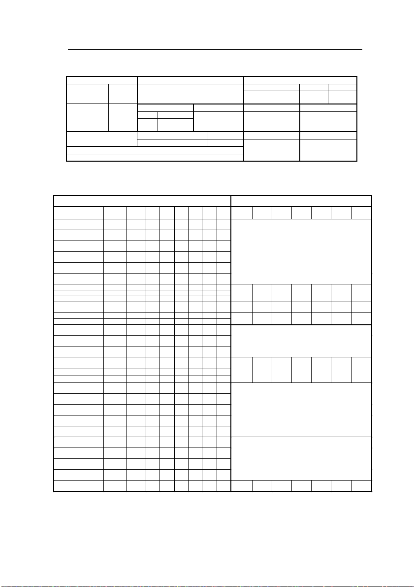
Appendix 39
Additional Jumper Settings
CMOS clear: JP5 Auto Voltage Detect Disable: JP1 CPU Cooling Fan: JP43
Retain CMOS 1Ð2 Remove this jumper cap if you use an pin 1 2 3
data (default) older type of CPU which can not be
Clear CMOS 2-3 Burst Mode: JP22 TB LED Reset HDD LED
data 1Ð2 Intel, AMD Connect the turbo Connect the reset Connect the HDD
DIMM Voltage: JP37 3.3V DIMM (default) 1-3, 2-4 Speak KB Lock
Power switch: PW2 to this jumper power LED to
identified correctly
2Ð3 Cyrix LED to this
jumper
5V DIMM 3-5, 4-6 Connect the speaker Connect keylock &
Connect your power switch to this jumper (momentary switch type) jumper J17
function GND 12V GND
button to this
jumper
LED to this jumper
Settings for Various Processors: SW1 & JP30
CPU Frequency: SW1 CPU Voltage: JP30
Bus
Processor
AMD K5 PR75 50MHz 1.5x off off off on on on
AMD K5 PR90 60MHz 1.5x off off off on off off
AMD K5 PR100 66MHz 1.5x off off off off off off
AMD K5 PR120 60MHz 1.5x off off off on off off
AMD K5 PR133 66MHz 1.5x off off off off off off
AMD K5 PR166 66MHz 2.5x on on off off off off
AMD K6 PR166 66MHz 2.5x on on off off off off dual
AMD K6 PR180 60MHz 3.0x off on off on off off 2.9V close open close open open open
AMD K6 PR200 66MHz 3.0x off on off off off off
AMD K6 PR233 66MHz 3.5x off off off off off off dual
AMD K6 PR266 66MHz 4.0x on off on off off off dual
AMD K6 PR300 66MHz 4.5x on on on off off off 2.2V open close open open open open
Cyrix 6x86(L) P150
Cyrix 6x86(L) P166
Cyrix 6x86(L) P200
Cyrix MX PR166 60MHz 2.5x on on off on off off dual
Cyrix MX PR200 66MHz 2.5x on on off off off off 2.9V close open close open oenp open
Cyrix MX PR233 75MHz 2.5x on on off off on off
Cyrix MX PR266 66MHz 3.5x off off off off off off
P54C P75 60MHz 1.5x off off off on on on
P54C P90 60MHz 1.5x off off off on off off
P54C P100 66MHz 1.5x off off off off off off
P54C P120 60MHz 2.0x on off off on off off
P54C P133 66MHz 2.0x on off off off off off
P54C/P55C P150 60MHz 2.5x on on off on off off
P54C/P55C P166 66MHz 2.5x on on off off off off
P54C/P55C P180 60MHz 3.0x off on off on off off
P54C/P55C P200 66MHz 3.0x off on off off off off
P55C P233 66MHz 3.5x off off off off off off dual
+
+
+
Multi-
Clock
plier 1 2 3 4 5 6
60MHz 2.0x on off off on off off
66MHz 2.0x on off off off off off
75MHz 2.0x on off off off on off
Voltage 1-2 3-4 5-6 7-8 9-10 11-12
Due to the various versions and voltages of AMD K5
and K6, please verify the correct voltage settings before
doing any installation
close open open close open open
3.2V
Due to the various versions and voltages of Cyrix
6x86(L), please verify the correct voltage settings
before doing any installation
Due to the various versions and voltages
of P54C (standard Pentium), please verify
the correct voltage settings before doing
any installation
The P55C (MMX) processors have the same voltage
setting: 2.8V
close open open open open close
2.8V
Page 44

40
Drivers Guide
ETEQ Drivers Installation Guide
Step 1 : South Bridge Identify Issue
ETEQ south bridge chipset can not be identified by Windows 95 and so it shows two
question marks under ‘Device Manager’. Therefore, we provide drivers for you to
solve this problem. Please find the Setup.exe file from the \rev-10\utility\Eteq_USB
directory under your CD-ROM that came with your motherboard and install it.
Step 2 : IDE Bus Master/Ultra DMA Drivers
If you have IDE devices that support Bus Master or Ultra DMA function, you need to
install the drivers to enable these functions. Please find the Setup.exe file from the
\rev-10\utility\Eteq_IDE directory under your CD-ROM that came with your
motherboard and install it.
Page 45

Drivers Guide
41
How to use AGP on the 5ED5/M-(T2)
Because AGP is a very new technology, enabling the use of AGP on your
5ED/M-(T2) board requires you to go through a lot of complicated steps.All the
necessary steps are described below, step through them one by one, then installing
all the necessary drivers should not be a problem.
1.) First of all, it is impossible to use the AGP port with a version of windows
lower than OSR2. Users of an older version of windows should upgrade to
OSR2. You can check what version of windows you have installed by
taking the following steps: click 'start', 'settings', 'control panel' and select
'system' there. Under the 'General' tab you will find what version of
Windows you have installed. If there is a B or a C at the end of the system
description then you have installed OSR2. Users of windows 98 (Memphis)
can use AGP as well. Users of NT will need to run NT5 to make use of
AGP.
2.) Now enter the BIOS setup by pressing the <Delete> during boot-up. Go to
the 'Chipset Features Setup' section of the BIOS setup and
make sure that the 'AGP' item there is set to 'enabled'.
3.) You will now have to install USBSUPP.EXE from Microsoft, which
includes the USB supplement and a new memory manager (VMM32.VxD)
needed for the AGP DIME feature. You can find this file on the OSR2 CD,
in the directory \OSR2\USBSUPP. (Make sure your OSR2 CD support USB)
4.) Install the VXD driver from this directory -> \rev-10\utility\Eteq_AGP\
setup.exe in your CD-ROM.
5.) Next you will have to install Direct X5 to your system. This is a set of
drivers provided by Microsoft for free, but you will have to download them
from their Internet Site. Go to the following address to download the
drivers: http://www.microsoft.com/directx/default.asp and download
'DirectX 5.0 for end users'. After downloading install it to your
system and restart your system.
6.) Install the drivers that came with your AGP card, and after restarting your
system you should be ready to make full use of your system's AGP port.
7.) In order to verify whether or not you really have successfully installed all
the necessary components, please take the following steps: Open the
'Microsoft DirectX-5 SDK' and double click on 'Direct X viewer'. Switch to
'DirectDraw Devices'. If there are numbers given for the following items:
'Video', 'Video (local)', 'Video (Non Local)' and 'texture', it means that you
have succeeded, because your system now allows your AGP card to make
use of the main memory for storage of image and texture data. If there is no
memory selected for these items then AGP is not enabled, please go through
the above steps to see if you forgot something.
Page 46

42
BIOS Update
New item in CHIPSET FEATURES SETUP
New BIOS a dd a item in “ CHIPSET FEATURES SETUP” and it ’ s
“SUSTAINED 3T WRITE” (or “DIRTY BIT”).
Enabled : Set the L2 cache dirty bit to 0.
Disabled : Set the L2 cache dirty bit to 1.
Note : Please refer to page 13 for detail information about the relation
between Dirty bit and Cacheable range.
 Loading...