


6KB
82440 LX PCI Mainboard
User’s Guide &
Technical Reference

®
E
™
About This Guide
This UserÕs Guide is for assisting system manufacturers and end users in setting
up and installing the mainboard. Information in this guide has been carefully
checked for reliability; however, no guarantee is given as to the correctness of the
contents. The information in this document is subject to change without notice.
Copyright Notice
Copyright 1997, Soyo Computer Inc. All rights reserved. This manual is
copyrighted by Soyo Computer Inc. You may not reproduce, transmit, transcribe,
store in a retrieval system, or translate into any language, in any form or by any
means, electronic, mechanical, magnetic, optical, chemical, manual, or otherwise,
any part of this publication without express written permission of Soyo Computer
Inc.
Trademarks
Soyo is a registered trademark of Soyo Computer Inc. All trademarks are the
property of their owners.
Disclaimer
Soyo Computer Inc. makes no representations or warranties regarding the
contents of this manual. We reserve the right to revise the manual or make
changes in the specifications of the product described within it at any time
without notice and without obligation to notify any person of such revision or
change. The information contained in this manual is provided for general use by
our customers. Our customers should be aware that the personal computer field is
the subject of many patents. Our customers should ensure that they take
appropriate action so that their use of our products does not infringe upon any
patents. It is the policy of Soyo Computer Inc. to respect the valid patent rights of
third parties and not to infringe upon or assist others to infringe upon such rights.
Restricted Rights Legend
Use, duplication, or disclosure by the Government is subject to restrictions set
forth in subparagraph (c)(1)(ii) of the Rights in Technical Data and Computer
Software clause at 252.277-7013.
Product Rights
Product mentioned in this manual are mentioned for identification purpose only.
Product names appearing in this manual may or may not be registered trademarks
or copyrights of their respective companies.
If you need any further information, please come to our home page on internet.
The address is Òhttp://www.soyo.com.twÓ.
Edition: November 1997
Version 2.0
Tested To Comply
C
C
F
With FCC Standards
FOR HOME OR OFFICE US
6KB SERIAL

iii
Table of Contents
Chapter 1: Introduction .................................................. 1
Key Features ............................................................................... 1
Unpacking the Mainboard........................................................... 2
Electrostatic Discharge Precautions............................................ 2
Mainboard Layout w/ Default Settings ....................................... 3
Chapter 2: Hardware Setup ............................................ 5
Jumpers ....................................................................................... 5
JP5: CMOS Clear Jumper .................................................... 5
SW1: Bus Fraction Core/Bus Ratio Select Jumper .............. 6
CPU Type Configuration ............................................................ 6
686 (PII) Ð 166 CPU Settings (2.5 x clock) .................. 6
686 (PII) Ð 200 CPU Settings (3 x clock) ..................... 7
686 (PII) Ð 233 CPU Settings (3.5 x clock) .................. 7
686 (PII) Ð 266 CPU Settings (4.0 x clock) .................. 7
686 (PII) Ð 300 CPU Settings (4.5 x clock) .................. 7
Memory Configuration ............................................................... 8
Multi I/O Port Addresses ............................................................ 8
Connectors .................................................................................. 9
ATX PW Ñ ATX Power Supply Connectors ....................... 9
PS/2 Keyboard Connector ..................................................... 9
PS/2 Mouse Connector.......................................................... 9
IR Ð IR Connector ............................................................... 10
Keylock & Power LED Connector...................................... 10
SPK Ð Speaker Connector ................................................... 10
RST Ð Hardware Reset Control ........................................... 10
IDE1/IDE2 Ð On-board Primary/Secondary IDE HDD
Connectors ........................................................................... 10
COM1/COM2 Connectors................................................... 11
IDE LED Ð IDE HDD LED Connectors ............................. 11
FDC Connector ................................................................... 11
PRT Ð Parallel Port Connector ............................................ 11
USB1/USB2 Ð Universal Serial Bus Connector ................. 11
PWRBT Ð ATX Power Supply On/Off Switch Connector
(Momentary Type)............................................................... 11
FAN: CPU Cooling Fan Connector ................................... 12
JP44 Ð Wake-On-LAN (WOL) Header ............................... 12
Slot 1 Installation Guide ........................................................... 13

iv
Chapter 3: BIOS Setup.................................................. 19
Standard CMOS Setup .............................................................. 20
BIOS Features Setup ................................................................. 21
Chipset Features Setup.............................................................. 23
Power Management Setup ........................................................ 26
PNP/PCI Configuration Setup .................................................. 28
Load Setup Defaults.................................................................. 29
Load BIOS Defaults.................................................................. 30
Integrated Peripherals ............................................................... 30
Supervisor Password ................................................................. 33
User Password ........................................................................... 34
IDE HDD Auto Detection ......................................................... 35
Chapter 14 Drivers Installation Guide......................... 36
MS-DOS/WINDOW/WFW ................................................ 36
WINDOWS NT3.5/4.0........................................................ 36
WINDOWS 95 .................................................................... 37
NOVELL 3.X&4.X ............................................................. 37
SCO UNIX .......................................................................... 37
SCO UNIX 5.0 .................................................................... 38
OS/2 2.0 and WARP 3.X..................................................... 39
Quick Installation Guide ................................................ 40
Motherboard Layout............................................................ 40
CPU Jumper Settings........................................................... 40
Memory Configurations ...................................................... 41
Connectors and Jumper Settings ......................................... 41
Default I/O Settings ............................................................. 41

1 Introduction
The 82440 LX PCI mainboard is a high-performance ATX architecture
system board that supports 686 (PII) family CPUs. This mainboard is
fully compatible with industry standards, and adds many technical
enhancements.
Key Features
¥ Processor supports:
Ñ 686 (PII) CPU up to 66 MHz host bus frequency (233 ~ 333
MHz)
Ñ auto detection of CPU voltage
Ñ Slot 1 support
¥ DRAM controller:
Ñ supports 4 strips of 168-pin EDO /SDRM Unbuffered
DIMM
Ñ supports auto detection of memory type
Ñ supports ECC or Parity configuration
Ñ has onboard memory configurations from 8MB to 512MB
¥ BUS controller:
Ñ complies with the PCI specifications v2.1
Ñ four 32-bit PCI slots (Masters), three ISA slots, and 4-layer
PCB
Ñ supports Universal Serial BusÑUSB (Optional)
¥ Peripheral controller:
Ñ System BIOS built-in NCR4.0 SCSI/SY-S8115 SCSI/SY-V325-
2M Card BIOS and ÒPlug and PlayÓ function
Ñ onboard built-in PCI Master IDE controller and floppy
controller
Ñ onboard supports for two high speed UARTS (w/i 16550 FIFO)
and Multimode parallel port for Standard, Enhanced (EPP) and
high speed (ECP) modes, PS/2 mouse function
Ñ onboard supports FLASH Memory for easy upgrade BIOS
Ñ onboard supports IR function
Ñ One 32-bit AGP slot onboard

2 Introduction
Unpacking the Mainboard
The mainboard package contains:
¥ The 82440LX Mainboard
¥ This User's Guide
¥ One Triones IDE Bus Master Drivers Diskette
Note: Do not unpack the mainboard until you are ready to install it.
Follow the precautions below while unpacking the mainboard.
1. Before handling the mainboard, ground yourself by grasping an
unpainted portion of the systemÕs metal chassis.
2. Remove the mainboard from its anti-static packaging and place it on
a grounded surface, component side up.
3. Check the mainboard for damage. If any chip appears loose, press
carefully to seat it firmly in its socket.
Do not apply power if the mainboard appears damaged. If there is
damage to the board contact your dealer immediately.
Electrostatic Discharge Precautions
Make sure you ground yourself before handling the mainboard or other
system components. Electrostatic discharge can easily damage the
components. Note that you must take special precaution when handling
the mainboard in dry or air-conditioned environments.
Take these precautions to protect your equipment from electrostatic
discharge:
¥ Do not remove the anti-static packaging until you are ready to install
the mainboard and other system components.
¥ Ground yourself before removing any system component from its
protective anti-static packaging. To ground yourself grasp the
expansion slot covers or other unpainted portions of the computer
chassis.
¥ Frequently ground yourself while working, or use a grounding strap.
¥ Handle the mainboard by the edges and avoid touching its
components.
Introduction 3
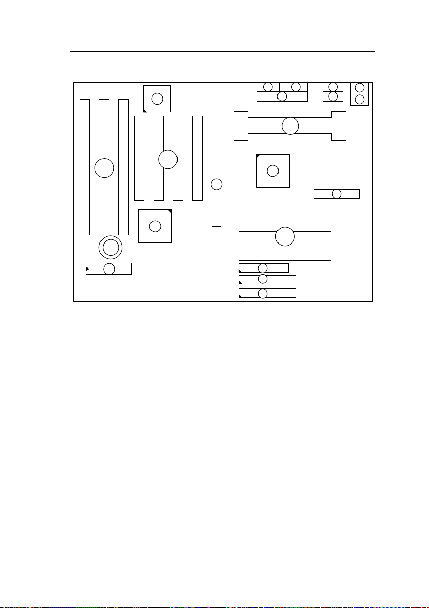
Mainboard Layout w/ Default Settings
1111
3
12
1
15
13
15
14
5
8
2
2
16
7
17
6
4
Figure 1Ð1. Mainboard Layout
1. Slot 1 for PII CPU 9. IDE1/IDE2 Connector
2. 82440LX Chipset 10. Floppy Connector
3. Ultra I/O Chip 11. COM1/COM2 Connector
4. PnP FLASH BIOS 12. Parallel Port Connector
5. ISA Slot 13. PS/2 Keyboard Connector
6. PCI Slot 14. PS/2 Mouse Connector
7. DIMM Memory Bank 15. USB 1/2 Connector
8. AGP Port 16. ATX Power Connector
17. CMOS Battery (Lithium
10
9
9
battery, 3V)

4 Introduction
Default settings are as follows: 686 (PII) 233MHz CPU, On-board
PCI Bus IDE Enabled, FDC Enabled, 2 high speed UARTS Enabled
(w/ 16550 FIFO), 1 EPP/ECP port (ECP + EPP mode), and ATX
Power Supply.
83977FX
JP44
IR
156
COM2 COM1 USB1
PRT
10
USB2
1
Slot 1 (for Pentium II CPU)
PS/2
KB
Conn.
PS/2
Mouse
Conn.
JP5
IDE
LED
82371 AB
1
PCI SLOT
SW1
ON
54231
82443LX
AGP Port
#1
#2#3#4
1
FAN
ATX PW
DIMM 1
DIMM 2
DIMM 3
DIMM 4
FDC
IDE2
IDE1
ISA SLOT
#3 #2 #1
3V
Lithium
Battery
FLASH
BIOS
Keylock
+–+–+ –
PW
LED
RST PWRBT
+–+–
TB
LED
SPK
Figure 1Ð2. Mainboard Default Setting
Important: Make sure the system is well ventilated to prevent
overheating and ensure system stability.

2 Hardware Setup
This chapter explains how to configure the mainboardÕs hardware. After
you install the mainboard, you can set jumpers, install memory on the
mainboard, and make case connections. Refer to this chapter whenever
you upgrade or reconfigure your system.
CAUTION: Turn off power to the mainboard, system chassis, and
peripheral devices before performing any work on the
mainboard or system.
Jumpers
JP5: CMOS Clear Jumper
Clear the CMOS memory by momentarily shorting this jumper; then
open the jumper to retain new settings.
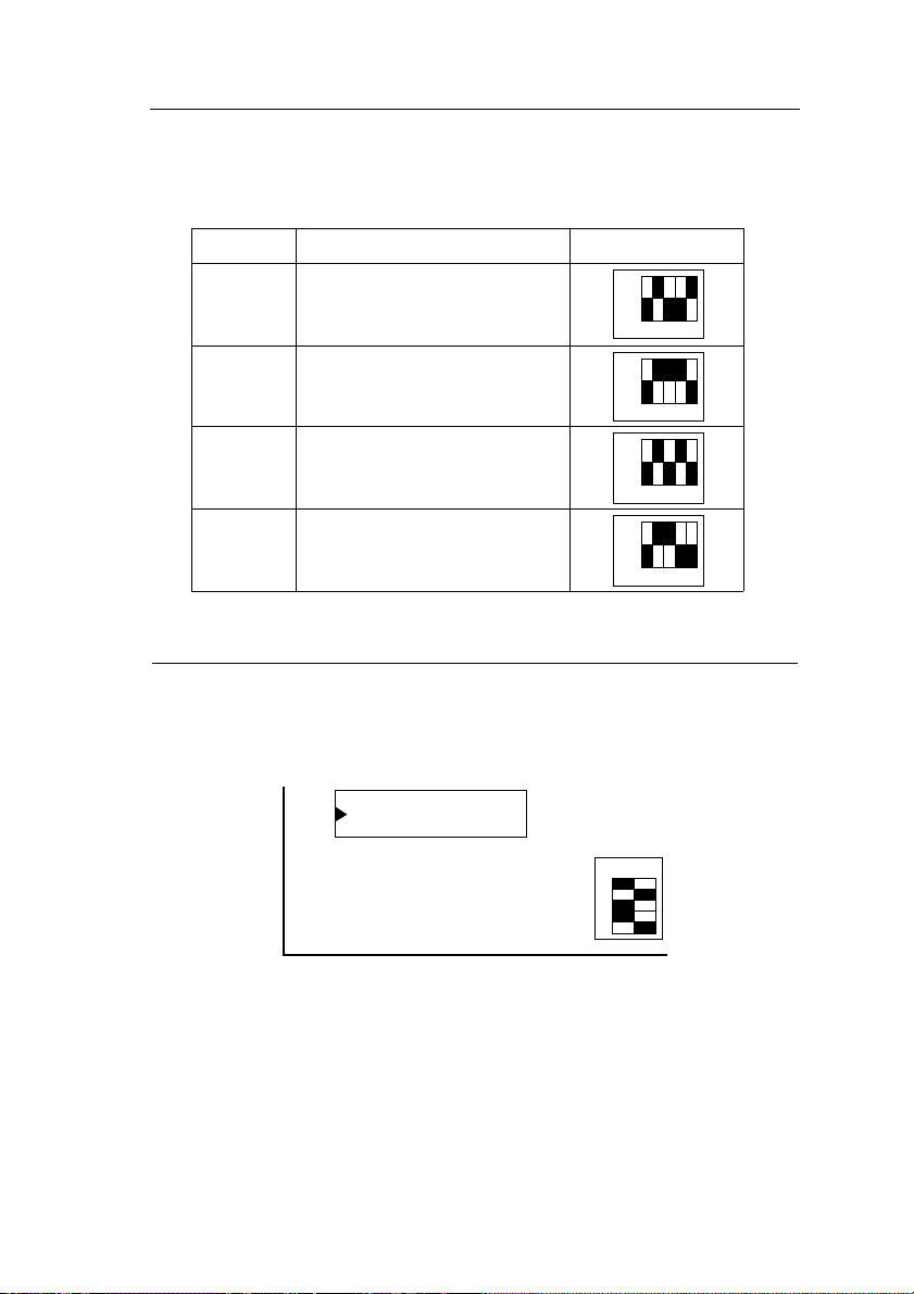
CMOS Setting JP5
Retain CMOS data
(default)
Clear CMOS data
1
1
6 Hardware Setup
SW1: Bus Fraction Core/Bus Ratio Select Jumper
Set this jumper according to your CPU clock.
Ratio 686 (PII) Family SW1
3.5x
686 (PII) Ð 233 MHz
(default)
ON
54231
ON
4.0x 686 (PII) Ð 266 MHz
ON
54231
4.5x 686 (PII) Ð 300 MHz
54231
ON
5.0x 686 (PII) Ð 330 MHz
54231
CPU Type Configuration
Set the mainboardÕs CPU switch SW1 according to CPU type as
described below.
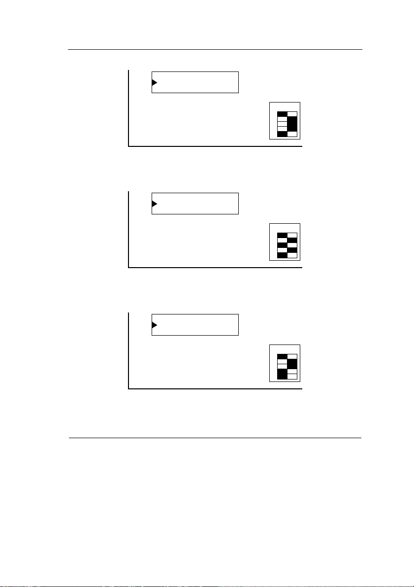
686 (PII) Ð 233 CPU Settings (3.5 x clock)
FLASH
BIOS
SW1
ON
54231
Figure 2Ð1Ð1. CPU Jumper Settings
Hardware Setup 7
686 (PII) Ð 266 CPU Settings (4.0 x clock)
FLASH
BIOS
Figure 2Ð1Ð2. CPU Jumper Settings
686 (PII) Ð 300 CPU Settings (4.5 x clock)
FLASH
BIOS
Figure 2Ð1Ð3. CPU Jumper Settings
686 (PII) Ð 330 CPU Settings (5.0 x clock)
FLASH
BIOS
SW1
ON
54231
SW1
ON
54231
SW1
ON
54231
Figure 2Ð1Ð4. CPU Jumper Settings
Memory Configuration
The mainboard supports four banks of 168-pin 3.3V EDO/SDRM
Unbuffered DIMM. The mainboard supports from 8 to 512 Mbytes
with no other restrictions on memory configurations. You can install
DRAM in any combination without having to rely on a memory
configuration table. Memory configuration is thus ÒTable-FreeÓ in any
bank.
8 Hardware Setup
Multi I/O Port Addresses
Default settings for multi-I/O port addresses are shown in the table
below.
Port I/O Address IRQ Status
LPT1* 378H 7 ECP + EPP
COM1 3F8H 4
COM2 2F8H 3
* If default I/O port addresses conflict with other I/O cards (e.g. sound
cards or I/O cards), you must adjust one of the I/O addresses to avoid
address conflict. (You can adjust these I/O addresses from the BIOS.
Note: Some sound cards have a default IRQ setting for IRQ7, which may
conflict with printing functions. If this occurs do not use sound
card functions at the same time you print.
Connectors
Attach the mainboard to case devices, or an external battery, via
connectors on the mainboard. Refer to Figure 1-1 for connector locations
and connector pin positions.
ATX PW — ATX Power Supply Connectors
The motherboard provides an ATX power supply connector. It is a
twenty-pin male header connector. Plug the connector from the power
directly onto the board connector while making sure the pin1 is in its
position.
3.3V
–12V
GND
PS-ON
GND
GND
GND
–5V
5V
5V
3.3V
3.3V
GND
5V
GND
5V
GND
PW-0K
5VSB
12V
PS/2 Keyboard Connector
A six-pin female PS/2 keyboard connector is located at the rear of the
board. Plug the keyboard jack into this connector.
Hardware Setup 9
PS/2 Mouse Connector
A six-pin female PS/2 mouse connector is located at the rear of the
board. Plug the mouse jack into this connector.
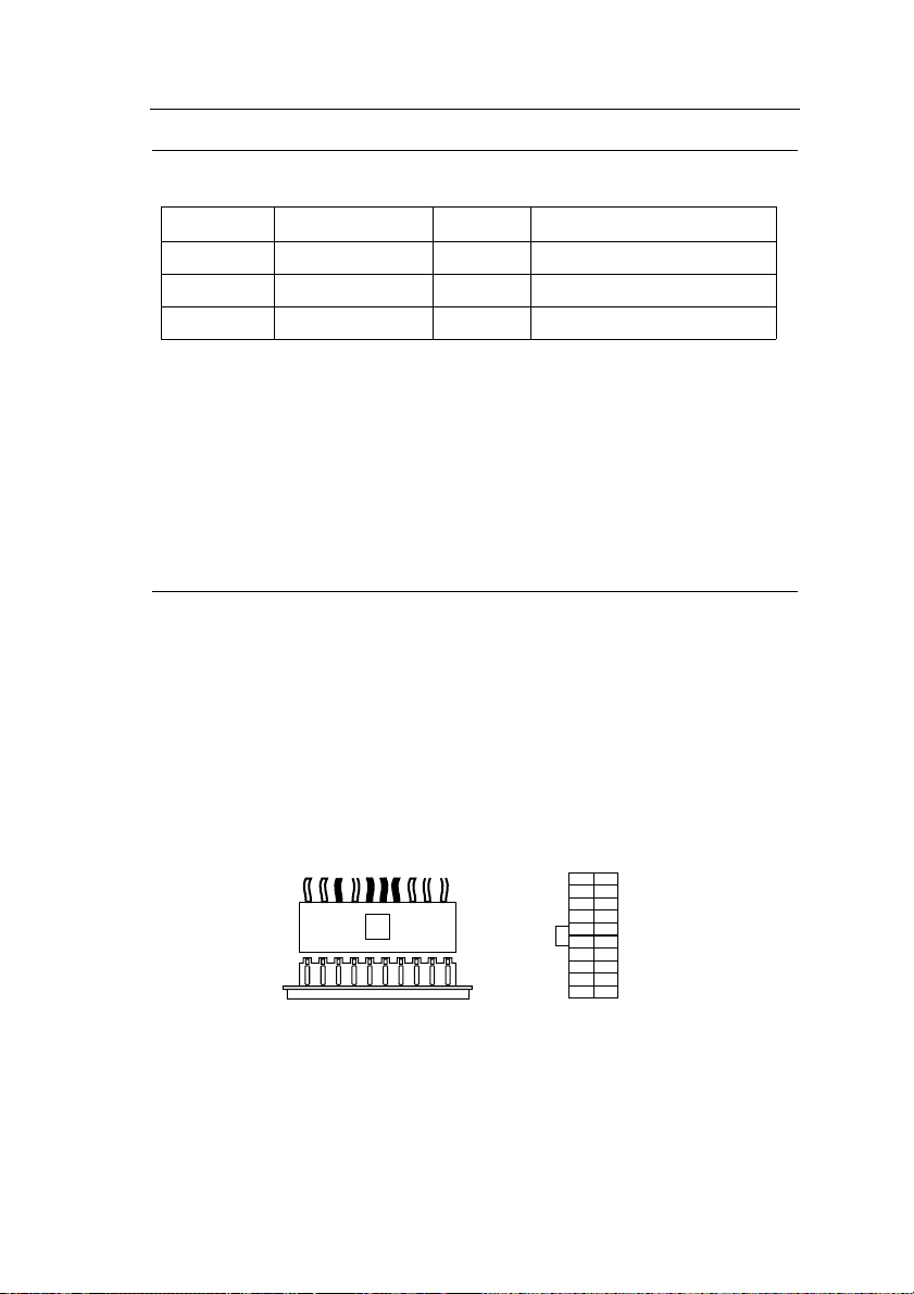
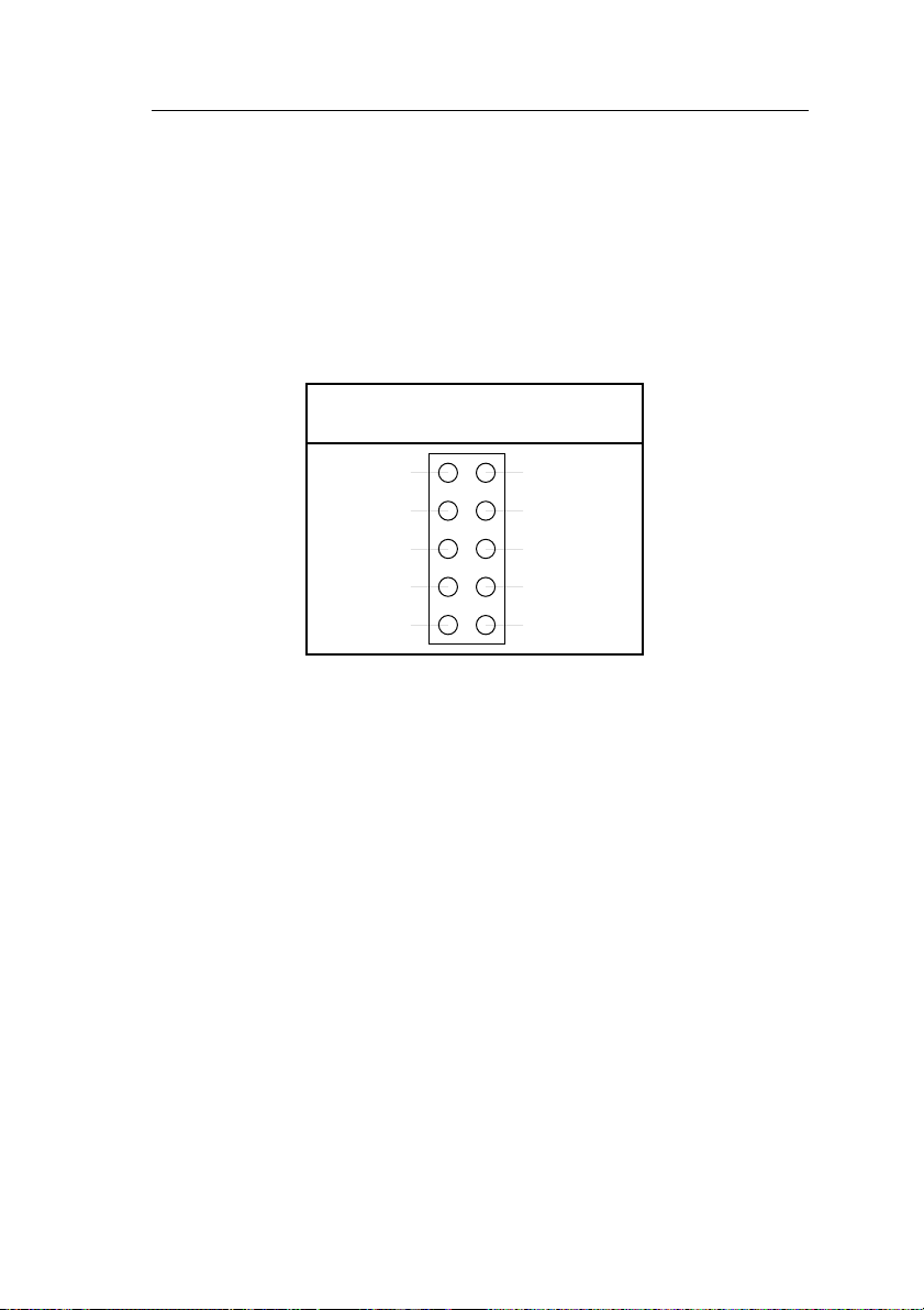
IR – IR Connector
A ten-pin wafer connector is for connecting to the IR device. Use the
device that has the ASKIR or HPSIR specification and choose
ASKIR/HPSIR from the BIOS setup.
IR Connector
Pin Assignment
VCC 1
FIRRX 2
IRRX 3
GND 4
IRTX 5
There are two ways to use this IR function. One is to connect a 5-pin IR
device and treat it like an ordinary IR port. The other way is to connect a
10-pin IR device and use the advanced ÒIR Wake UpÓ PC function. Ask
your IR provider for the new ÒIR Wake UpÓ function.
6 Empty
7 CIRRX
8 VSB
9 Empty
10 Empty
Keylock & Power LED Connector
This connector is for a lock that may be installed on the system case for
enabling or disabling the keyboard. This connector also attaches to the
caseÕs Power LED. (Pin 1, 3 for power LED, pin 4, 5 for keylock.)
SPK – Speaker Connector
Attach the system speaker to connector SPK.
RST – Hardware Reset Control
Attach the Reset switch to RST. Closing the Reset switch restarts the
system.

10 Hardware Setup
IDE1/IDE2 – On-board Primary/Secondary IDE HDD
Connectors
Attach on-board hard disk drives to these connectors.
COM1/COM2 Connectors
Connect COM1/COM2 devices to these connectors.
IDE LED – IDE HDD LED Connectors
Attach on-board IDE device LEDs to this connector. The LED lights
when an IDE device is active.
FDC Connector
Attach floppy cable to this connector.
PRT – Parallel Port Connector
Attach parallel port cable to this connector.
USB1/USB2 – Universal Serial Bus Connector
Attach USB cable to these connectors for external USB device.
PWRBT – ATX Power Supply On/Off Switch Connector
(Momentary Type)
Attach a two-pin switch to this connector for turning the ATX power
supply on/off.
 Loading...