

Page 1

SEMC Troubleshooting Manual
ABOUT
Troubleshooting Manual
W890
W890
ABOUT TROUBLESHOOTING MEASUREME NT POINTS
1217-3942 rev. 1
APPENDIXCOMPONENT OVERVIEW FUNCTIONAL OVERVIEW
1 (119)
Page 2

ABOUT Contents
SEMC Troubleshooting Manual
W890
ABOUT
General information
The purpose of this document is to provide enhanced technic al information for Sony Ericsson
repair technicians in order to assist during service, repair and troubleshooting operations on Sony
Ericsson mobile phones. It should be used as a c omplement to other repair instructions and tools
as notified by the local Sony Ericsson repre sentative.
To search for components throughout the entire document use the “search” function in Adobe
Acrobat Reader 7.0 (or later version) and enter the component name or other word. Use zoom to
enlarge.
For easier navigation of the document you can use the bookmarks that appear in the Bookmarks
tab on the left side of the Adobe Acrobat Reader window. Each bookmark jumps to a page in the
document.
Disclaimer
This document is Sony Ericsson confidential and should be t reated as confi dential in accordance
with the agreement with Sony Ericsson. This document is intended for use by authorized service
technicians only. Sony Ericsson is not to be held responsible for any damages or losses caused
intentionally or unintentionally due to unauthorise d use of the information in this document.
Revision Hi st o ry
Rev. Date Changes / Comment s
1
09/01/2008 Initital revision.
ABOUT
About 2
Contents 2
TROUBLESHOOTING
Equipme nt L ist 3
On/Off Problems 8
Flash Problems 8
Dead Phone Problems 9
Display Problems 10
Display Illumination Problems 11
Key Problems part 1 11
Key Problems part 2 12
LED Problems 12
Main and VGA Camera Proble ms 13
Vibrator Problems 13
Charging Problems 14
USB/VBUS Charging Problems 14
SIM Problems 15
Memory Stick Problems 15
Audio Internal Problems 16
Audio External Problems 16
FM Radio Problems 17
Bluetooth Problems 17
GSM Network Problems 18
WCDMA Network Probl em s 19
System Connector Protection Test 20
Current Consumption Test 20
Battery an d Cur r ent C alibr ati o n Test 22
Backup Capacitor Test 22
Charging Test 23
ASIC Revision Test 23
Antenna Switch Test 24
Reference Measurement Points 25
Measurement Points Pictures 26
MEASUREMENT POINTS
Front S ide 39
Back Side 40
SIM FPC 41
Top Schematic 42
Audio Top 43
Audio Analog 44
Audio Digital 45
Audio FM Radio 46
Perform ance & Applicat i o ns Top 47
System Top 48
System Control - Clo c ks & Re s et s 49
System - Memorie s 50
System - PoP Interface 51
Power Top 52
Power - Regulators & Charging 53
Power - Camera 54
Power - ASICs 55
Power - Memories 56
Connectivity Top 57
Connectivi ty - ADC & I2C 58
Connectivity - Cards 59
Connectivity - USB, SYScon 60
Connectivity - Keypad 61
Imaging Top 62
Imaging - Display 63
Imaging - Camera 64
Access Top 65
Access - GS M & UMTS 66
Access - GSM Top 67
Access - GS M PA 68
Access -GSM Edge R X 69
Access - U M TS Top 70
Access - U M TS Control 71
Access - U M TS D upl ex 72
Access - U M TS RX 73
Access - UM TS S y nt hesizer 74
Access - UM TS PA 75
Access - Blueto ot h 76
Test 77
COMPONENT OVERVIEW
Front S ide 78
Back Side 79
FUNCT IONAL OVERVI EW
Technical Description 80
Block Diagrams 89
APPENDIX
Replaceable Parts 91
Components - B1260, B2100, B3100 92
Components - D2105, D2400, L 2200 93
Components - L2401-02 93
Components - L24 0 3- 04, L2407-08 93
Components - L2405-06, N1200, N1230 94
Components - N1300, N1380 95
Components - N1400, N2201, N2202 96
Components - N2203, N22 04 97
Components - N2205, N2402 97
Components - N2424, N3100 98
Components - N3101, N4201 98
Components - V22 02 , V240 2 98
Components - V2405 , V2420 98
C omponen ts - X1100, X1203, X1400 99
Components - X220 0, X2400 99
Components - Z1230 100
Components - Z4200, Z4201, Z4202 100
Components - Display 100
Components - Cam er a Fl ex Mo dul e 101
Components - SIM M 2 Fl ex Mo dule 102
Components - Key FPC 103
Troubleshooting Software Document at i o n 104
Troubleshooting Fixture Setup Instructions 111
Setup & Maintenance Instr uc t i on 113
for W890 TRS Fi xture
ABOUT
1217-3942 rev. 1
2 (119)
Page 3

TROUBLESHOOTING Equipment List
SEMC Troubleshooting Manual
W890
W890 Equipment List
Note: More additional information about the equipment used for TRS can be found in Repair
Tools Catalogue on CSPN or on the following location: CSPN – Repair Instructions – Electrical –
W890 – Equipment List.
Power Supply Channel 2 DCIO/SEPI
Agilent 6632B or similar
Location: CSPN-Repair Instructions-Level: Mechanical-Tool Catalogue
Instrument Settings:
Voltage: 5.0 Volt
Limiter: 2A
Note: It is very important to follow instrument setting instructions when performing the
Current Calibration Test.
Oscilloscope
Tektronix TDS 2012 or similar
Location: CSPN-Repair Instructions-Level: Mechanical-Tool Catalogue
Digital Multimeter (DMM)
Fluke 83 or similar
Location: CSPN-Repair Instructions-Level: Mechanical-Tool Catalogue
The 0, 64 mm Test Probes is recommended by Sony Ericsson when DMM is in use see picture 1.
Picture 1
TROUBLESHOOTING
TRS Fixture Kit
Location: CSPN-Repair Instructions-Electrical-W890-Equipment List
Dummy Battery
Location: CSPN-Repair Instructions-Electrical-W890-Equipment List
Part number: NTZ 112 533
Instruments
Power Supply Channel 1 VBATT
Agilent 6632B or similar
Location: CSPN-Repair Instructions-Level: Mechanical-Tool Catalogue
Instrument Settings:
Voltage: 3.8 Volt
Limiter: 2A
Note: During the calibration the accurate voltage from the VBATT must be within ±0.015 V. If
this is not fulfilled it will result in a faulty calibration. (For more information about
recommended power supply units, see the Repair Tool Catalogue on CSPN under the Mechanical
level. The Power Supply Channel 1 VBATT must allow reverse current.
Note: Maximal cable length between the Power Supply Channel 1 VBATT and the dummy
battery must be maximum 1m. The cable must have a capacity for at least 16A.
Spectrum Analyzer
HP 8595E or similar
Location: CSPN-Repair Instructions-Level: Mechanical-Tool Catalogue
RF probe
HP 85024A or similar
Location: CSPN-Repair Instructions-Level: Mechanical-Tool Catalogue
Mobile Phone Tester
Yokogawa VC230 or similar
Location: CSPN-Repair Instructions-Level: Mechanical-Tool Catalogue
FM Signal Generator
Agilent E4433B or similar
Location: -
Note: It is very important to follow instrument settings instructions when performing the
Battery Calibration Test.
1217-3942 rev. 1
3 (119)
Page 4

TROUBLESHOOTING Equipment List
SEMC Troubleshooting Manual
W890
RF Adaptor
Adaptor 33 N-BNC-50-1
Adaptor to Signal Generator RF Output
See Picture 2
Location: -
Picture 2
PC Package & PC Software
PC Package (Computer)
Location: CSPN-Repair Instructions-Level: Mechanical-Tool Catalogue
Urquell Fault Trace SW with project file
Location: CSPN-Repair Instructions-Electrical-W890-Trouble Shooting Application
Project File: W890 Project_R1A
Cables
USB Computer Cable
Location: CSPN-Repair Instructions-Level: Mechanical-Tool Catalogue
See Picture 4.
Picture 4
TROUBLESHOOTING
DSU-60/USB Cable
Location: CSPN-Repair Instructions-Level: Mechanical-Tool Catalogue
Part number: KRY 101 1413
RF Test Cable Flexible
Location: CSPN-Repair Instructions-Level: Mechanical-Tool Catalogue
Part number: RPM 119 885
See Picture 5.
Picture 5
Drivers
SEPI BOX Drivers
Location: EMMA III-Drivers-SEPI
SE Communication Interface SEPI BOX
Location: CSPN-Repair Instructions-Level: Mechanical-Tool Catalogue
Part number: LTN 214 1484
See Picture 3.
Picture 3
SEPI Interface Cable – A1
Location: CSPN-Repair Instructions-Level: Mechanical-Tool Catalogue
Part number: KRY 101 1119/1
See Picture 6.
Picture 6
1217-3942 rev. 1
4 (119)
Page 5

TROUBLESHOOTING Equipment List
SEMC Troubleshooting Manual
W890
Power Cable RED to Power Supply Channel 1 VBATT
Maximum Length: 1m
Location: CSPN-Repair Instructions-Level: Mechanical-Tool Catalogue
Power Cable BLACK to Power Supply Channel 1 VBATT
Maximum Length: 1m
Location: CSPN-Repair Instructions-Level: Mechanical-Tool Catalogue
Customized Power Supply Channel 2 DCIO/SEPI Cable
To perform Current Calibration the phone must be supplied directly through the system
connector. Customize the cable according to following instructions:
STEP 1:
Take the CST-75 battery charger and cut of the charger according to Picture 7.
Picture 7
STEP 4:
Connect DCIO and SEPI Interface Cable – A1 cables according to Picture 10.
Picture 10
TROUBLESHOOTING
Wrong setup.
Picture 11
Note: Cable length must be exact 1.3m.
STEP 2:
Connect the CST-75 charger Red or White wire to the Plus Output and the Black wire to the
Minus (GND) Output at Power Supply Channel 2 DCIO/SEPI according to Picture 8.
Picture 8
STEP 3:
Cut of isolation material from inside of the charger plug according to Picture 9.
Picture 9
Power Supply Channel 2 DCIO/SEPI Cable Connection Setups
Correct DCIO/SEPI Cable setup when TRS Fixture is used.
Picture 12
Note: Example of DCIO/SEPI and K750 TRS Fixture Setup.
1217-3942 rev. 1
5 (119)
Page 6

TROUBLESHOOTING Equipment List
SEMC Troubleshooting Manual
W890
Correct DCIO/SEPI Cable setup when the Dummy Battery is used.
Picture 13
Picture 14
STEP 2:
Cut the Red lab plug according to Picture 16
Picture 16
TROUBLESHOOTING
STEP 3:
Use any Hands free (PHF) Cable and cut according to Picture 17
Picture 17
Customized FM Radio Cable
STEP 1:
Use Cable according to Picture 15
Picture 15
Product Name: Test lead BNC-4mm 1,5m
Product Description: Test lead with 4 mm lab plugs at one end and a BNC plug at the other.
Manufacturer: PMK Germany
Location: http://www.elfa.se/en/
or other supplier.
Part number: 46-310-40 (Note: This is ELFA part number)
Note: Minimum Cable length 40 cm.
STEP 4:
Use only wire connected to Pin2 and cut all rest wires according to Picture 18.
Use digital multimeter instrument (DMM) and perform diode measurement to select wire
connected to Pin2 at hands free system connector plug.
Picture 18
1217-3942 rev. 1
6 (119)
Page 7

TROUBLESHOOTING
Equipment ListEquipEquipment Listment List
SEMC Troubleshooting Manual
W890
STEP 5:
Connect by soldering cable from Picture 16 and cable from Picture 18 according to Picture 19.
Picture 19
Test Cards
Local SIM
Any functional Local SIM Card, see Picture 20
Picture 20
Rohde & Schwarz RF Shield Package (Box)
Location: CSPN-Repair Instructions-Level: Mechanical-Tool Catalogue
Part number: -
Picture 23
TROUBLESHOOTING
SMK RF Probe
Location: CSPN-Repair Instructions-Level: Mechanical-Tool Catalogue
Part number: SXA 109 6356
Test SIM GSM/UMTS
One Test SIM GSM/UMTS is needed to perform Current Consumption Test, see Picture 21.
Location: To buy a Test SIM GSM/UMTS, please contact your supplier of test equipment.
Picture 21
Sony Memory Stick M2
Any functional Memory Stick Micro M2 Card, see Picture 22
Picture 22
Picture 24
RF Adapter for RF Sheild Box
Location: CSPN-Repair Instructions-Level: Mechanical-Tool Catalogue
Part number: See picture 25.
Picture 25
1217-3942 rev. 1
7 (119)
Page 8
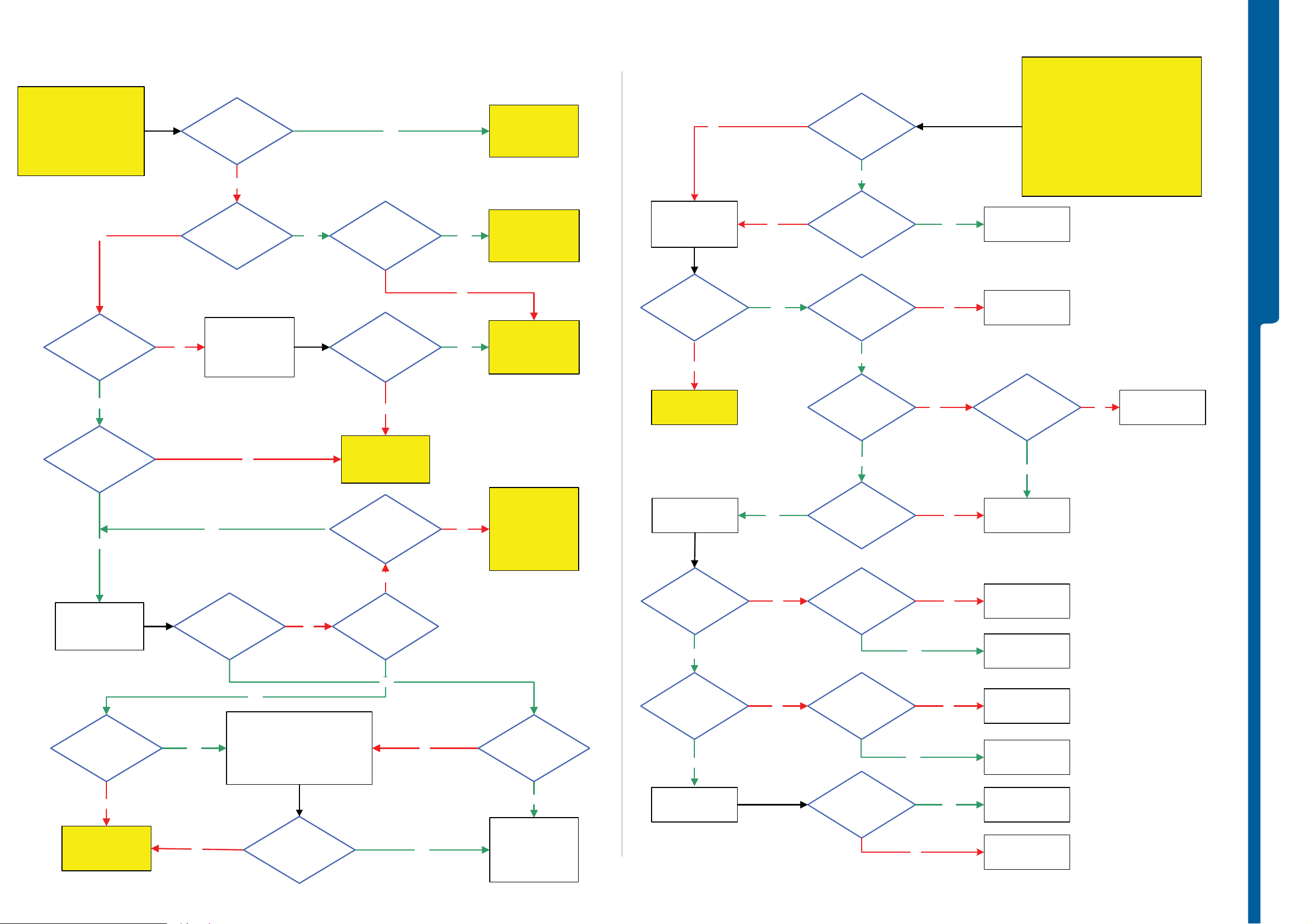
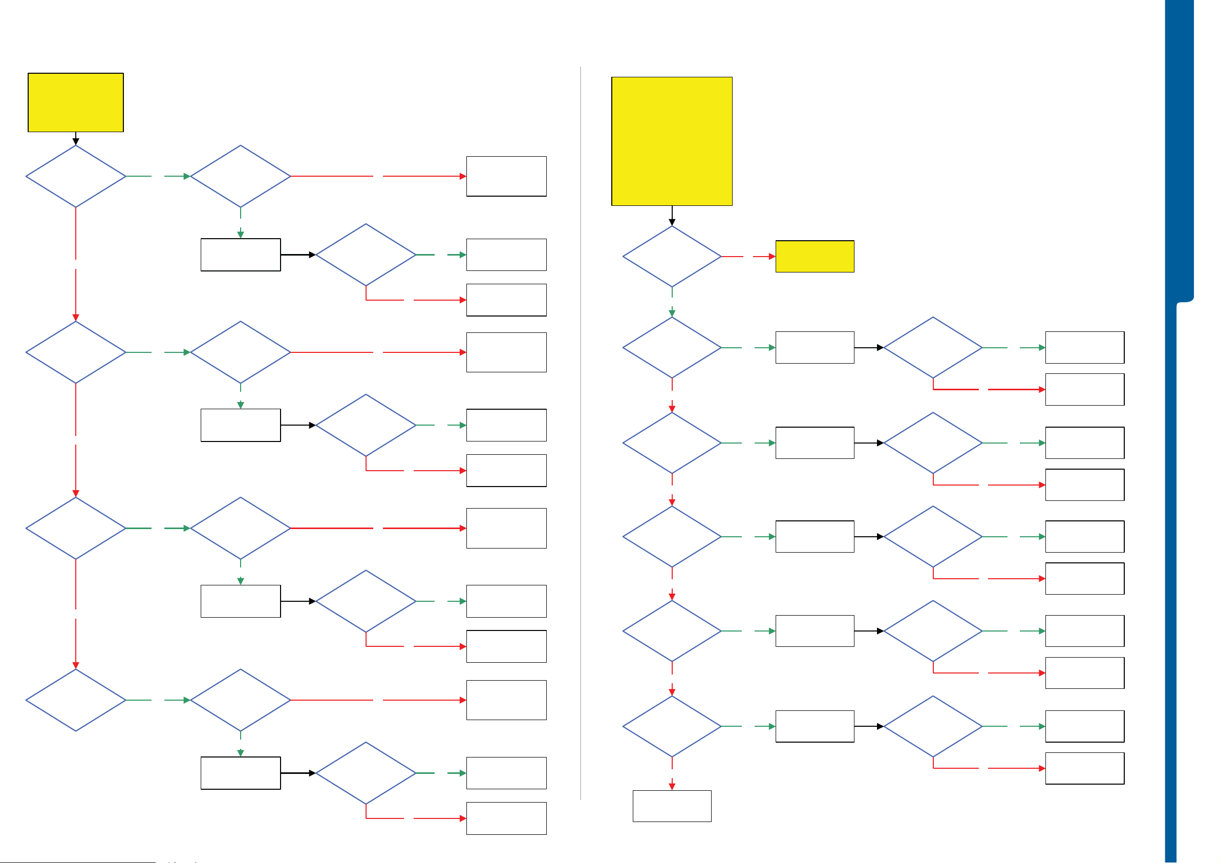
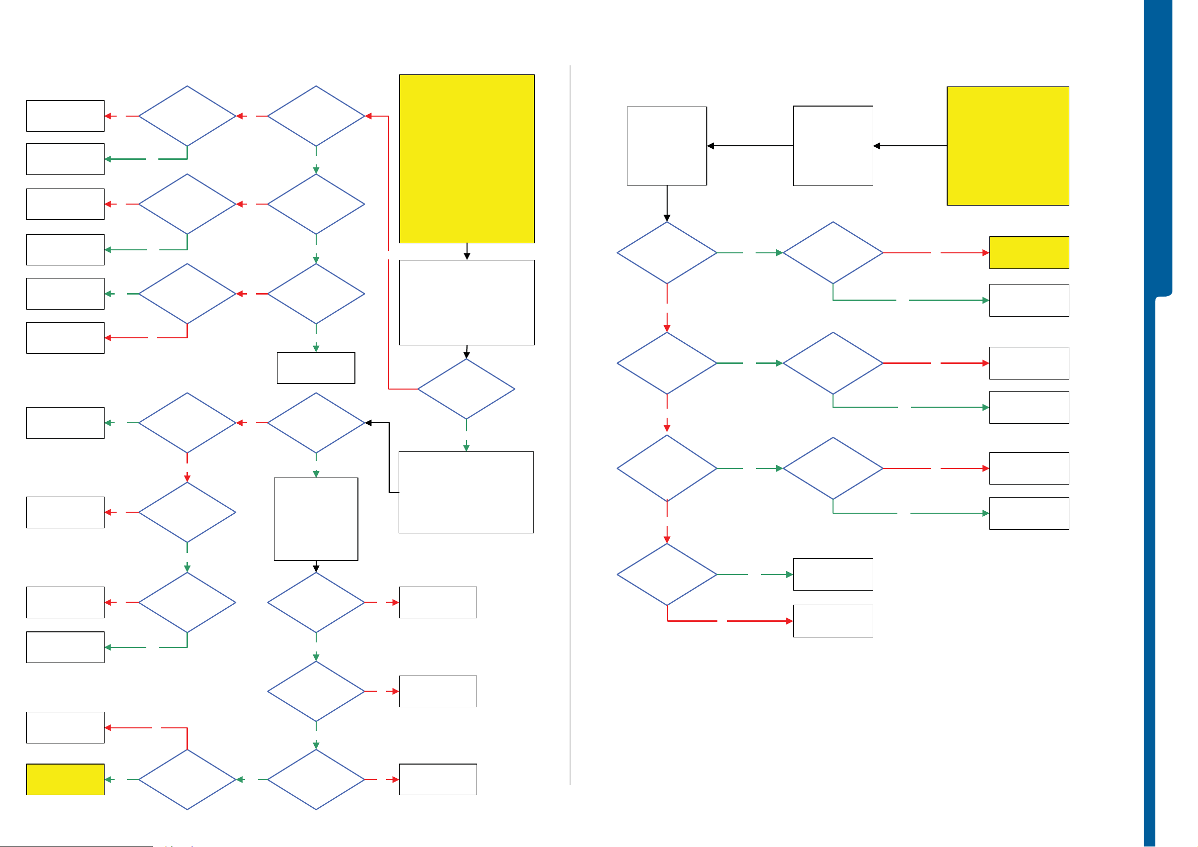
START
Use
Dummy Battery (VBATT)
No
On/Off Problems
Is the phone
consuming more than
1mA when the phone
is powered off
No
Is it possible to
power on the phone
Yes
Yes
Is it possible to power
off the phone
TROUBLESHOOTING On/Of f Prob lem s - Flash Proble m s
Flash process
Start-up when using
ITP SW by using
Yes
Go to
Dead phone
Problems part 1
Go to
Current
Consumption Test
After this go to
Charging Test.
No
Power Up the Phone
Connect
USB Cable From PC
No
Flash Problems
EMMA III SW
Yes
Download
EMMA III SW
Is Download
Passed
Yes
SEMC Troubleshooting Manual
W890
START
Step 1:
Perform System Connector Protection Test
If successful go to step 2.
Step 2:
Phone with Normal SW
Use TRS Fixture
Connect:
Display, Keyboard Flex Module and VBATT
and try to Flash the phone by using
EMMA III SW
TROUBLESHOOTING
SL 5 Replace
D2020
SL 4 Escalate
Is the
phone consuming
any current when
powering on the
phone
Yes
Is the current
consumption between
10mA to 70mA
Yes
Flash
the phone with
correct CDA
software
Connect a charger No
No
Yes
CDA Software
Flash
Successful
No
Is the phones
behavior as normal
Optimized
charging
No
Go to
Dead Phone
Problems part 1
Press
2 and 5
Connect USB
Run Pre-config 1 and 2
Run DPY/Z
Successful
Flash
No
Flash process
started
No
Yes
No
Go to
Key Problems
Go to
System Connector
Protection Test..
After this go to
Flash Problems
Is the phone
Indicate charging
No
Go to
USB/VBUS
Charging Problems
Disconnect the
phone from the
TRS Fixture
Max
2 Ohm between
MP 127 (X2400_Pin 10)
and MP 126
(Z2400_Pin 3)
Yes
Yes
No
5 Volt DC at
MP 131 (C2414)
Yes
3.3 Volt
Pk-Pk Pulses at
MP 124 (C2436)
Yes
1.8 Volt
Pk-Pk Pulses at
MP 112 (C2434)
Max
0.5 Ohm between
MP 127 (X2400_Pin 10)
and MP 125
(Z2400_Pin 2)
Yes
No
NoYes
No
No
SL 5 Replace
R2434
SL 4 Escalate
1.8 Volt DC
at
MP 97 (R2448)
Yes
Replace
D2400
Replace
System Connector
X2400
SL 5 Replace
Z2400
SL 4 Escalate
No
SL 5 Replace
D2000
SL 4 Escalate
Flash
The phone with
ITP software
successful
No
Go to
Flash Problems
No
Yes
1. Customize the phone into DPY/Z
2. Startup the phone and wait for
the configuration to ta ke place
(takes less than a minute)
3. Customize with correct CDA
4. Activate the phone
Problem
solved
Yes
NoYes
Yes
Problem
solved
Yes
Claim for a
SW Upgrade
Max
2 Ohm between
MP 129 (X2400_Pin11)
and MP 130
(Z2400_Pin 4)
Yes
Replace
N2424
No
Max
0.5 Ohm between
MP 129 (X2400_Pin 11)
and MP 130
(Z2400_Pin 1)
Problem
solved
Yes
No
No
Yes
Replace
System Connector
X2400
SL 5 Replace
Z2400
SL 4 Escalate
Claim Component
N2424
SL 5 Replace
D2000
SL 4 Escalate
1217-3942 rev. 1
8 (119)
Page 9
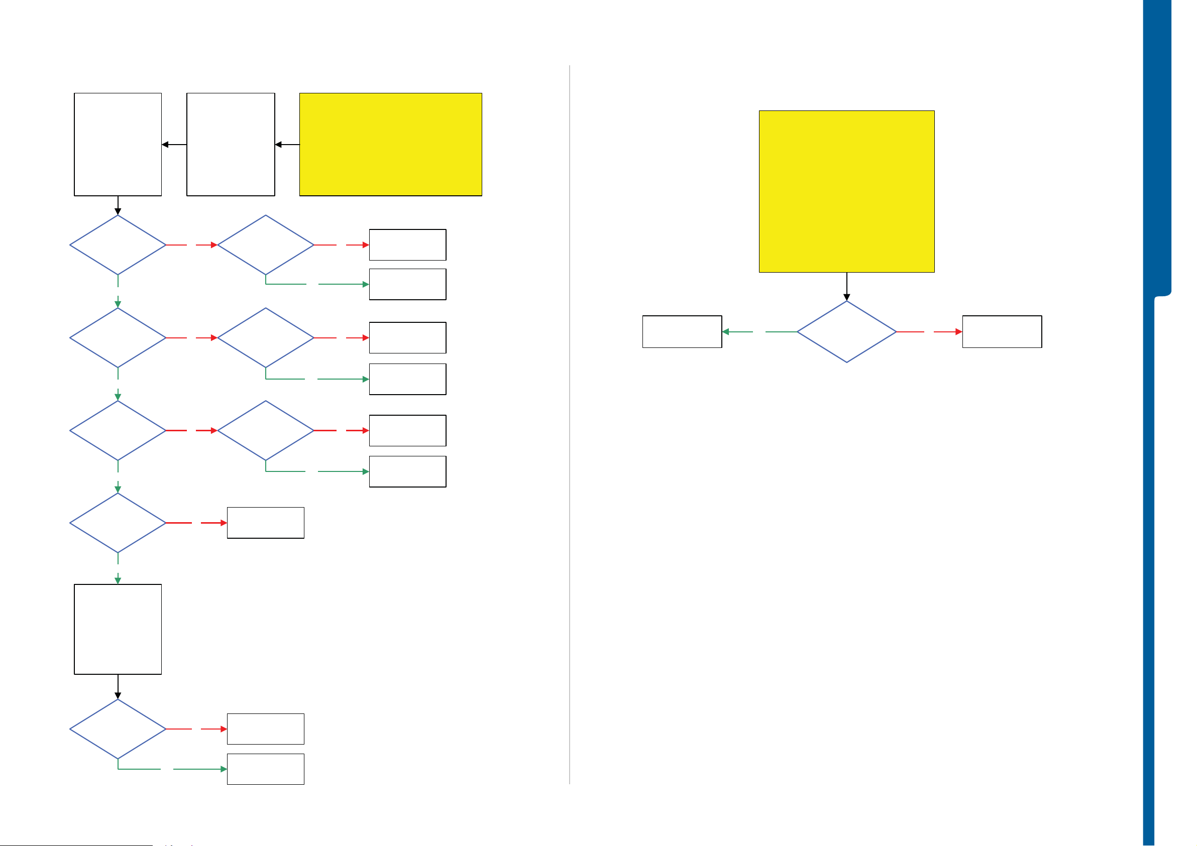
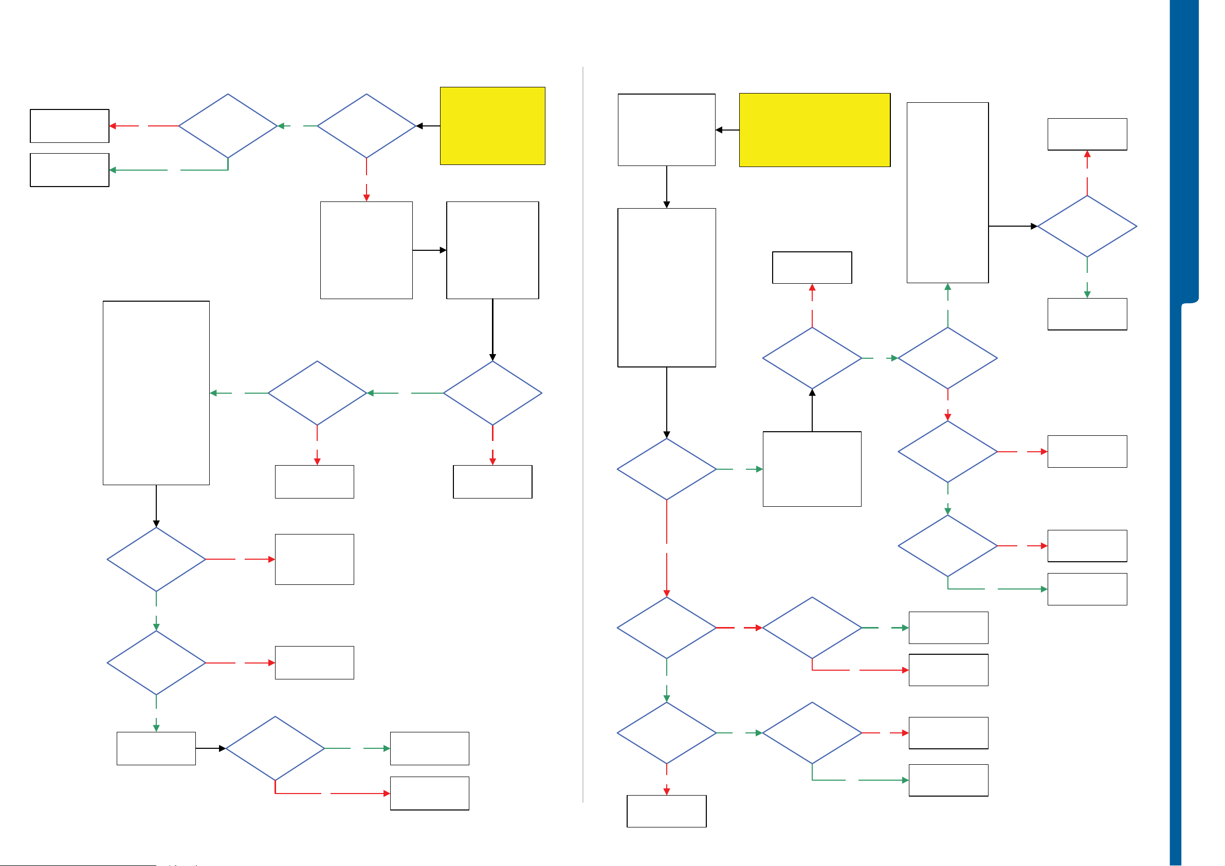
TROUBLESHOOTING Dead Phone Problems
SEMC Troubleshooting Manual
W890
START
Step 1:
Try to recover the phone by
using EMMA III SW
Press key 2 and 5
Connect USB Cable to the phone
Run pre-config 1 or 2
Run DPY/Z
If successful claim SW Flash
If not continue with step 2.
Step 2:
Use TRS Fixture
Connect Only: VBATT
Replace
N1230 or N1380
SL 5 Remove
N2000
SL 4 Escalate
Is the
current consumption
still more than
1mA
No
Replace
N1200
Yes
Yes
Yes
Dead Phone Problems part 1
Is the
current consumption
more than 1mA
Yes
Try to trace faulty
component by using
the freezing spray
Is
N1230 or N1380
getting hot
No
Try to trace faulty
component by using
the freezing spray
SL 5 Replace
N2000
SL 4 Escalate
26 MHz
at
MP 17 (R1263)
No
No
0 Volt DC
Between Power
Supply GND and
Shield Can
Fence
Yes
Connect
DCIO/SEPI
to the Phone
32 kHz
RTCCLK at
MP 73 (R2199)
Yes
26 MHz
MCLK at
MP 37 (R2100)
No
1.8V DC at
MP 21 (R1261
VDDE18) and 2.8V DC
at MP 19 (R1260
VccA)
Yes
SL 5 Replace
No
No
Check following voltages:
2.5V MP 79 (C2216 VANA25)
1.2V MP L2200 VCORE12
1.8V MP 82 (C2239 VCORE18)
2.7V MP 81 (C2205 VBT27)
2.6V MP 115 (C2209 VAUDIO26)
2.7V MP 116 (C2215 VDIG)
2.2V MP 69 (X2402_Pin A4
VBACKUP)
R2200
SL 4 Escalate
SL 4 Replace
B2100
if not successful then
Escalate to SL 5
SL 5 Replace
B2100 if not
successful then
Replace N2000
Yes
Dead Phone Problems part 2
START
NOTE !
Before following this guide
the Dead Phone Problems
part 1 TRS guide must be
finished!
VCORE12
Voltage
Ok
Yes
VCORE18
Voltage
Ok
No
No
Dead Phone Problems part 2
Is the
MP 100 (R2299)
Short circuit to
Shield Can
Fence
No
1.2 Volt DC
at MP 103
(V2206_Cathode)
Yes
Replace
L2200
Is
the any of
C2342 to C2347
Short circuit or
D2000 Getting
hot
No
No
1.8 Volt DC
at MP 83
(N2202_Pin 3)
Yes
3.8 Volt DC
at MP 104 (L2201)
Yes
Yes
Yes
No
SL 5 Check
C2220,C2219,V2206,
C2240,C2222,C2221
C2301 to C2305
C2307,C2308,C2311
C2314 to C2316
C2318,C2319,
C2322,C2324,D2000
SL 5 Replace
Faulty Component
and L2200
SL 4 Escalate
SL 5 Replace
L2201 and C2226
SL 4 Escalate
SL 5 Replace
V2206 or N2000
SL 4 Escalate
SL 5 Replace
Faulty Component
SL 4 Escalate
SL 5 Replace
C2239
SL 4 Escalate
TROUBLESHOOTING
Replace
B1260
SL 5 Replace
D2020
SL 4 Escalate
Go to
Flash Problems
SL 5 Replace
N2000
SL 4 Escalate
SL 4 Replace
N2202
SL 5 Replace
C2216 or
C2236 to C2330
Yes
No
No
ITP SW Flash
Successful
No
any of C2216 or
C2336 to C2330
Short circuit or
N2202 Getting
Yes
Is the
hot
Disconnect
VBATT and DCIO/SEPI
Connect: Display and
Keypad FPC to the PBA
Connect: VBATT
Activate EMMA III SW
Press the ”C” key and
connect USB Cable
Flash the Phone with
the ITP SW
VANA25
Voltage
Ok
Yes
Go to
Dead Phone
Problems part 2
Yes
Yes No
All voltages
Ok
No
Current
Consumption more
than 50mA
No
SL 5 Replace
N2000
SL 4 Escalate
Yes
VBT27
Voltage
Ok
Yes
Go to
Dead Phone
Problems part 3
No
Is
the any of
C2205 or C1409, Short
circuit or
N1400 Getting
hot
No
3.8 Volt DC
at MP 84 (N2202_Pin1)
and MP 86 (N2202_Pin4)
Yes
No
Yes
SL 5 Replace
No
C2238 and N2202
SL 4 Escalate
SL 4 Replace
SL 5 Replace
C2205 or C1409
SL 5 Replace
SL 4 Escalate
1217-3942 rev. 1
Replace
N2202
N1400
N2000
9 (119)
Page 10
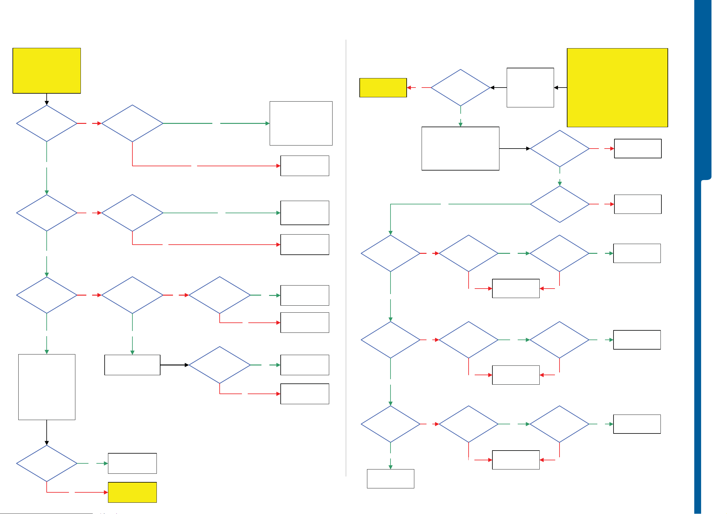
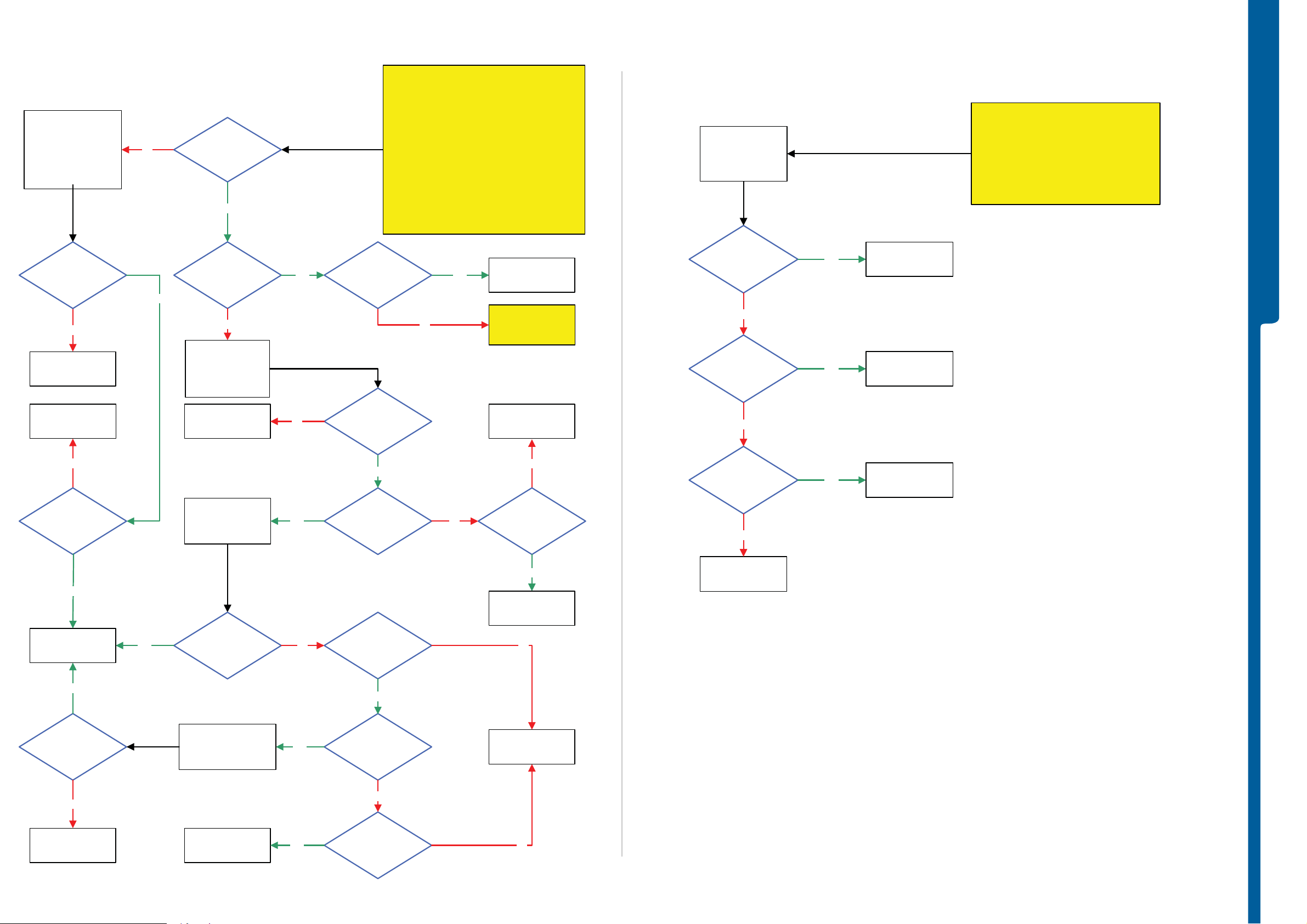
TROUBLESHOOTING Dead Phone Problems - Display Problems
SEMC Troubleshooting Manual
W890
START
Dead Phone Problems part 3
NOTE !
Before following this guide
the Dead Phone Problems
part 2 TRS guide must be
finished!
VAUDIO26
Voltage
Ok
Yes
VDIG
Voltage
Ok
Dead Phone Problems part 3
Is the
MP 115 (C2209)
No
No Yes
Short circuit to
Shield Can
Fence
Is
the any of
C2215,C1407
Short circuit or
N1400 Getting
hot
Yes
No
SL 4 Check and Replace
N2400, V2405 or X4201
SL 5 Check and Replace
N2000,C2209,C2400
C2473,V2406,C4213,
C3135 or C3136
SL 5 Replace
N2000
SL 4 Scrap
SL 4 Replace
N1400
SL 5 Replace
C2215 or C1407
Go to
Display illumination
Problems
No
Display Backlights
Ok
Yes
Turn off the phone
Disconnect: Display and Keypad
Start the phone and go to:
Fault trace SW
MMI
Display pattern
Init Screen Testing
Activate: TV Test Pattern
Yes
Display Problems
Fault trace SW
MMI
Display pattern
Init Screen Testing
Activate:
RGB Color Pattern
Display, Keyboard Flex Module and VBATT
1.8 Volt DC
at MP 30 (C4214) and
2.6 Volt DC at
MP 29 (C4213)
Yes
1.8 Volt DC
at MP 31 (C4227) and
0 Volt DC at
MP 33 (C4228)
START
Step 1:
Use TRS Fixture
Connect:
If Display working properly at the
TRS Fixture then replace Display
If not then continue with step 2.
Load ITP SW into the phone
Display problems TRS guide
Step 2:
Connect: DCIO/SEPI
and continue with
SL 5 Replace
No
No
N2000
SL 4 Escalate
SL 5 Replace
D2000
SL 4 Escalate
TROUBLESHOOTING
Yes
VBACKUP
Voltage
Ok
Yes
Disconnect
VBATT and DCIO/SEPI
Connect: Display and
Keypad FPC to the PBA
Connect: VBATT
Activate EMMA III SW
Press the ”C” key and
connect USB Cable
Flash the Phone with
the ITP SW
No
2.2 Volt DC
at MP 74 (C2218)
Yes
Disconnect
VBATT and DCIO/SEPI
No
No
Is
C2218
Short circuit
Is
R2204 ~ 4.7 KOhm
No
No
Yes
Yes
SL 5 Replace
N2000
SL 4 Escalate
SL 5 Replace
C2218
SL 4 Escalate
SL 5 Replace
N2000
SL 4 Escalate
Replace
X2402
SL 5 Replace
R2204
SL 4 Escalate
1.8 Volt DC at
MP Z4202_Pins
5,6,7,8
Yes
1.8 V
DC Pk-Pk
at MP Z4200_Pins 5,6,7,8
short after TV Test
was activated
Yes
1.8 V
DC Pk-Pk
at MP Z4201_Pins 5,6,7,8
short after TV Test
was activated
No
No
No
1.8 Volt DC at
MP Z4202_Pins
1,2,3,4
No
1.8 V
DC Pk-Pk
at MP Z4200_Pins 1,2,3,4
short after TV Test
was activated
No
1.8 V
DC Pk-Pk
at MP Z4200_Pins 1,2,3,4
short after TV Test
was activated
Yes
SL 5 Replace
D2000
SL 4 Escalate
Yes
SL 5 Replace
D2000
SL 4 Escalate
Yes
0 Ohm
Between
MP Z4202_Pins
5,6,7,8 and
TRS Fixture
GND
No
0 Ohm
Between
MP Z4200_Pins
5,6,7,8 and
TRS Fixture
GND
No
0 Ohm
Between
MP Z4201_Pins
5,6,7,8 and
TRS Fixture
GND
Yes
Yes
Yes
Replace
Z4202
Replace
Z4200
Replace
Z4201
ITP SW Flash
successful
No
Yes
SL 5 Replace
D2020
SL 4 Escalate
Go to
Flash Problems
Yes
Replace
X4201
No
SL 5 Replace
D2000
SL 4 Escalate
No
1217-3942 rev. 1
10 (119)
Page 11
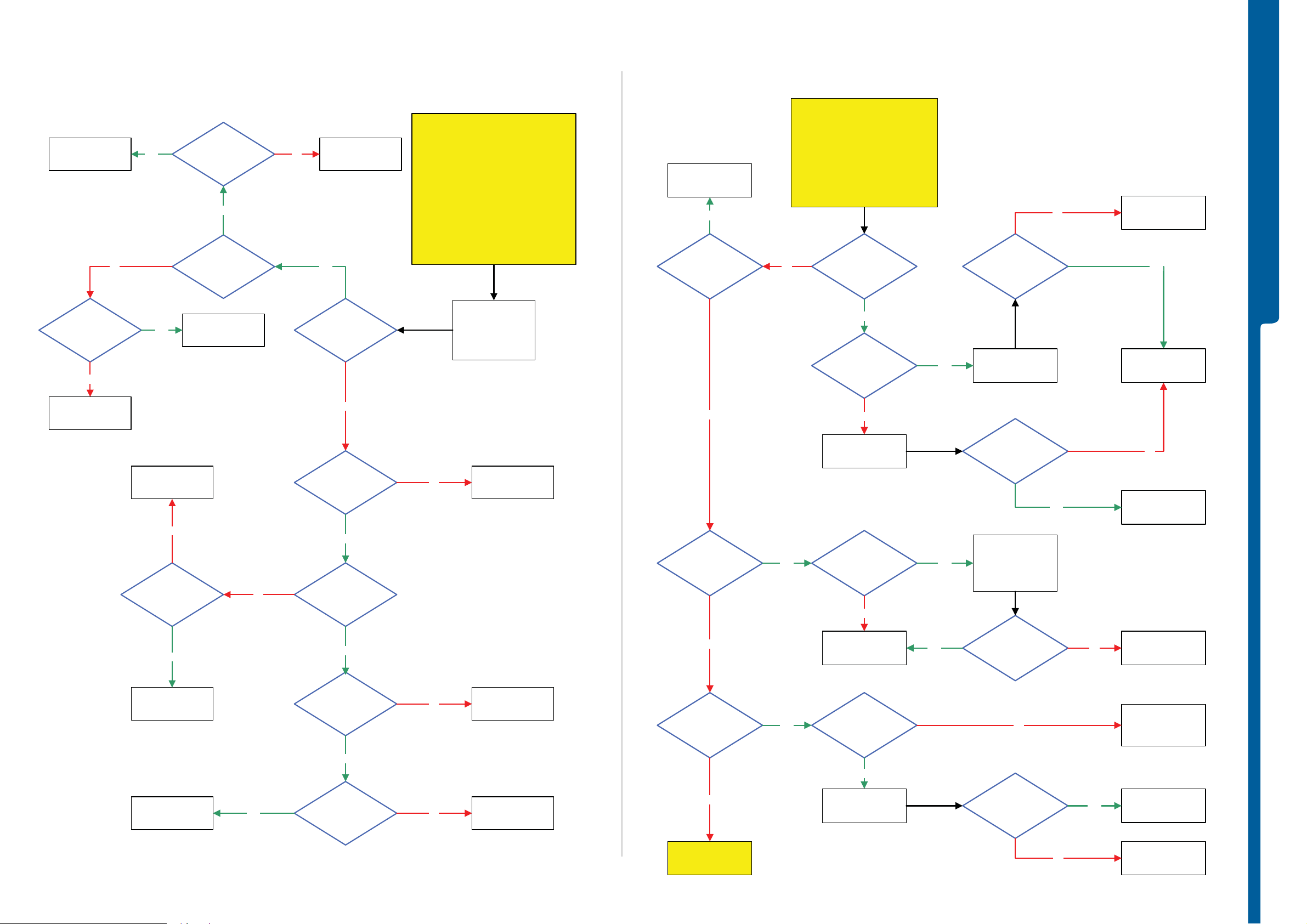
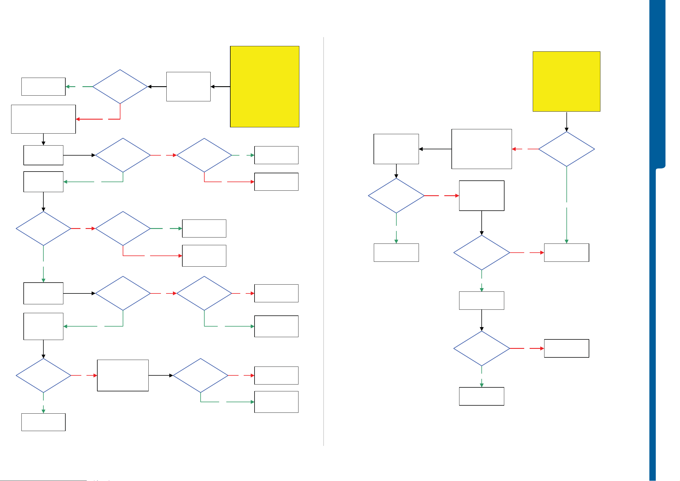
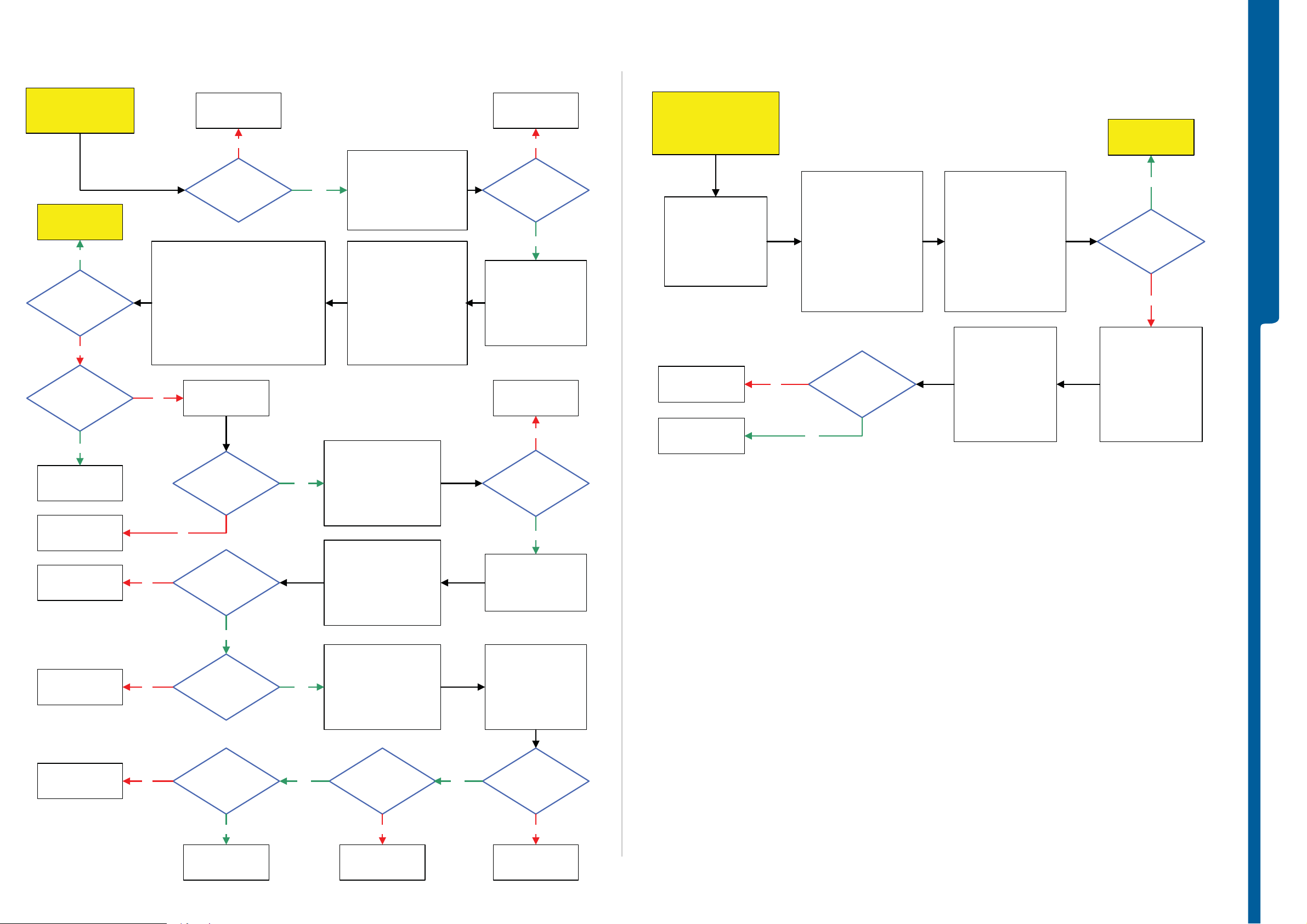
TROUBLESHOOTING Display Illumination Problems - Key Problems part 1
SEMC Troubleshooting Manual
W890
Flash with
EMMA SUCR SW
No
1.8 Volt
Pulses at
MP 89 (N2201_Pin 3)
Shortly after phone
Power On
No
SL 5 Replace
N2000
SL 4 Escalate
Yes
MP 90 (C2224 VOPTO30)
Yes
SL 5 Replace
L4200
SL 4 Escalate
No
Is
L4200
Max 0.8 Ohm
Display illumination Problems
More than
2.0 Volt Pulses at
MP 51 (V4201)
Shortly after phone
Power On
Yes
3.0 Volt
Pulses at
Shortly after phone
Power On
Replace
N2201
No
No
Display Backlights
Pulses at MP 107 (L4200)
Replace
X4300
Yes
Ok
No
3.8 Volt DC at
MP 105 (L4201)
Yes
More than
5.0 Volt Pk-Pk
shortly after Display
backlight
Is set
START
Replace Display and retest the phone. If
successful claim Display if not go to step 2.
Replace Camera Flex Module and retest
the phone. If successful claim
Camera Flex Module if not go to step 3.
Load ITP SW into the phone
Connect: Display and Camera Flex Module
Connect: VBATT and DCIO/SEPI
Display illumination problems TRS guide
No
Step 1:
Step 2:
Step 3:
Use TRS Fixture
and continue with
Use Fault trace SW
MMI
Misc
Init Screen Testing
Activate
Display Backlight
SL 5 Replace
L4201
SL 4 Escalate
Replace
V2402
Yes
Problem with
Phone Off
No
Problem with
Volume Down/Up
or Walkman
key
START
Use TRS Fixture
Display, Keyboard Flex Module,
No
Yes
Connect:
Camera Flex Module,
VBATT and DCIO/SEPI
Problem with
Phone On
Yes
3.7 Volt DC
At MP 41
(V2402_Cathode)
No
Disconnect the
Camera Flex Module
1.8 Volt DC
At MP 42 (C2464)
No
Key Problems part 1
Yes
Camera Flex Module
Volume Down/Up or
Yes
Camera Flex Module
0 Volt DC at
MP 41
(V2402_Cathode)
Press the
On/Off Key at
3.7 Volt DC
at MP 41
(V2402_Cathode)
Press the
Walkman key
at
No
Yes
Replace
TROUBLESHOOTING
X4300
Yes
SL 5 Replace
N2000
SL 4 Escalate
No
Replace
Camera Flex Module
Yes
SL 5 Replace
N2000
SL 4 Escalate
Replace
X4201
Yes
Yes
More than
15 Volt Pk-Pk
Pulses at MP 102 (C4202)
shortly after Display
backlights
Is set
Yes
0 Volt DC at
MP 77 (V4205_Pin C)
When Display
Backlight is
set
No
No
Replace
N4201
SL 5 Replace
V4205 or N2000
SL 4 Escalate
No
Problem
with ”Soft right”,
”Clear”,”Camera” or
”Rock right”
Key
No
Go to
Key Problems part 2
Yes
SL 5 Replace
D2000
SL 4 Escalate
1.8 Volt DC
At MP 24 (C2463)
Yes
Press the
Camera Key at the
Keypad FPC
Yes
0 Volt DC
At MP 42 (C2464)
No
0 Volt DC
At MP 24 (C2463)
No
No
Camera Flex Module
SL 5 Replace
C2463, R2468
SL 4 Escalate
SL 5 Replace
Yes
SL 4 Escalate
Keypad FPC
1217-3942 rev. 1
Replace
or X4300
or D2000
D2000
Replace
or X2401
11 (119)
Page 12
TROUBLESHOOTING Key Problems part 2 - LED Problems
SEMC Troubleshooting Manual
W890
Key problems part 2
NOTE !
Before doing this the
Key Problems part 1
TRS guide must be
finished
Problem
with ”End red”,
”1”,”2”, ”3" or
”Rock push”
Key
No
Problem
with ”Send green”
”7”,”8”, ”9" or
”Rock left”
Key
Yes
Yes
Key Problems part 2
1.8 Volt DC
At MP 25 (C2462)
Yes
Press the
Key ”3" at the
Keypad FPC
1.8 Volt DC
At MP 26 (C2461)
Yes
No
0 Volt DC
At MP 25 (C2462)
No
No
Yes
SL 5 Replace
C2462, R2469
or D2000
SL 4 Escalate
SL 5 Replace
V2428 or D2000
SL 4 Escalate
Replace
Keypad FPC
or X2401
SL 5 Replace
C2461, R2470
or D2000
SL 4 Escalate
START
Load ITP SW into the phone
Use TRS Fixture
Connect: Camera Flex Module,
Keyboard Flex Module, Display,
VBATT and DCIO/SEPI
Use Fault Trace SW
MMI
Activate:
Display Backlight
Upper Keypad, Middle Keypad
and Lower Keypad LED
Charge LED and Tally LED
Display
Backlight
Ok
Yes
Problem with
Tally LED
No
No
Yes
LED Problems
Go to
Display illumination
Problems
Disconnect the
Camera Flex Module
0 Volt DC at
MP 47 (X4300_Pin
B19)
No
Yes
TROUBLESHOOTING
Replace
Camera Flex Module
or X4300
SL 5 Replace
N2000
SL 4 Escalate
No
Problem
with ”Act” ”4”,”5”,
”6" or ”Rock up”
Key
No
Problem
with ”Soft left”
”
”,”0”, ”#" or
*
”Rock down”
Key
Yes
Yes
Press the
Key ”9" at the
Keypad FPC
1.8 Volt DC
At MP 27 (C2460)
Yes
Press the
Key ”6" at the
Keypad FPC
1.8 Volt DC
At MP 28 (C2459)
Yes
Press the
Key ”#" at the
Keypad FPC
0 Volt DC
At MP 26 (C2461)
No
0 Volt DC
At MP 27 (C2460)
No
0 Volt DC
At MP 28 (C2459)
No
No
Yes
Yes
Yes
SL 5 Replace
V2432 or D2000
SL 4 Escalate
Replace
Keypad FPC
or X2401
SL 5 Replace
C2460, R2471
or D2000
SL 4 Escalate
SL 5 Replace
V2424 or D2000
SL 4 Escalate
Replace
Keypad FPC
or X2401
SL 5 Replace
C2459, R2472
or D2000
SL 4 Escalate
SL 5 Replace
D2000
SL 4 Escalate
Problem with
Charge LED
No
Problem with
Upper Keypad LED
No
Problem with
Middle Keypad LED
No
Problem with
Lower Keypad LED
No
Yes
Yes
Yes
Yes
Disconnect the
Keypad FPC
Disconnect the
Keypad FPC
Disconnect the
Keypad FPC
Disconnect the
Keypad FPC
More than
1.8 Volt DC at
MP 23
(V2207_Cathode)
0 Volt DC at
MP 22 (X2401_Pin
A10)
0 Volt DC at
MP 18 (X2401_Pin
B8)
0 Volt DC at
MP 20 (X2401_Pin
A3)
No
No
No
No
Yes
Yes
Yes
Yes
Replace
Keypad FPC
or X2401
SL 5 Replace
N2000
SL 4 Escalate
Replace
Keypad FPC
or X2401
SL 5 Replace
N2000
SL 4 Escalate
Replace
Keypad FPC
or X2401
SL 5 Replace
N2000
SL 4 Escalate
Replace
Keypad FPC
or X2401
SL 5 Replace
N2000
SL 4 Escalate
No
Replace
Keypad FPC
or X2401
Flash the Phone with
EMMA SUCR SW
1217-3942 rev. 1
12 (119)
Page 13
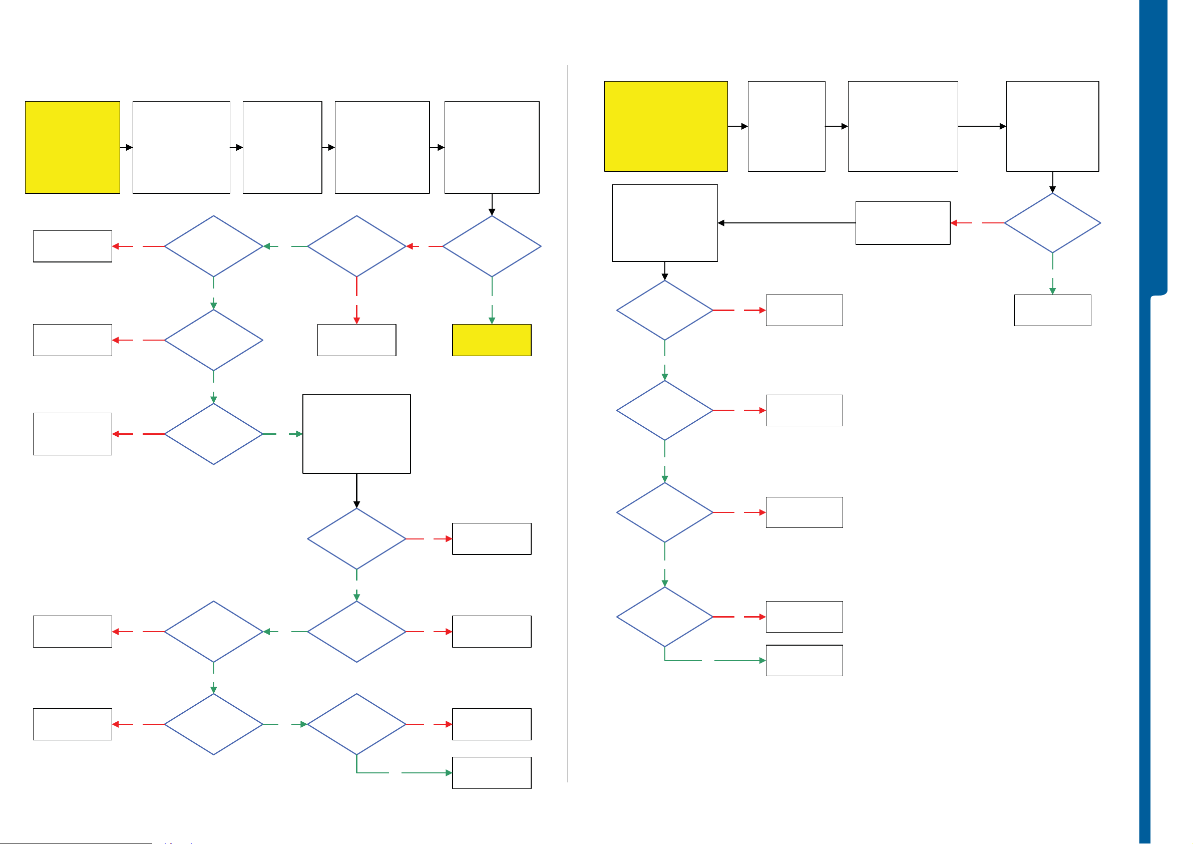
TROUBLESHOOTING Main and VGA Camera Problems - Vib r ator Proble ms
SEMC Troubleshooting Manual
W890
Fault trace SW
MMI
Misc
Activate:
Main Camera Test
1.8 Volt DC
at 40 (MP R2281
CAM_LDO_EN) and
MP 43 (C4330
CI_RESn)
Yes
1.9 Volt DC
at MP 38 (C2287
VCAMCORE_18)
Yes
Main and VGA Camera Problems
Load ITP SW into the
phone. Use TRS Fixture
Connect: Display and
Camera Flex Module
Connect:
VBAT and DCIO/SEPI
Use Fault Trace SW
No
No
C2281
Short circuit
Are any of
C2286 or C2287
Short circuit
Is
Flash the phone with EMMA SUCR SW and
If successful Claim SW Flash if not go to step 2.
Replace Camera Flex Module and r etest the phone.
If successful Claim Camera Flex Mo dule
Main and VGA Camera Problems TRS guide.
Yes
Yes
START
Step 1:
retest the phone
Step 2:
if not then continue with
SL 5 Replace
No
No
D2000
SL 4 Escalate
SL 5 Replace
C2281
SL 4 Escalate
Replace
N2204
SL 5 Replace
C2286 or C2287
SL 4 Escalate
Replace
X2401
Vibrator Problems
START
Replace Keyboard Flex Module
If successful claim Keyboard Flex Module
Load ITP SW into the phone
Connect: VBATT and DCIO/SEPI
Use Fault Trace SW and go to:
Continue with the Vibrator Problems TRS guide
Step 1:
and retest the phone
if not go to step 2.
Step 2:
Use TRS Fixture.
MMI
Misc
Activate:
Vibrator Test
2.8V-2.9V
Pk-Pk Pulses at
MP 75 (C4206
VIBR_OUT)
NoYes
TROUBLESHOOTING
SL 5 Replace
N2000
SL 4 Escalate
2.8V DC at
MP 45 (C2283
VCAM_28) and 1.8V DC
at MP 39 (C2284
VCAM_18)
Yes
13 MHz at
MP 48 (C4329)
And 26 MHz at
MP 46 (C4313)
Yes
Deactivate
Main Camera Test
and Activate
VGA Camera Test
Fault trace SW
MMI
Misc
Activate:
VGA Camera Test
No
No
Are any of
C2282, C2283 or C2284
Short circuit
SL 5 Replace
D2000
SL 4 Escalate
Yes
No
Replace
N2203
SL 5 Replace
C2282,C2283 or C2284
SL 4 Escalate
4.8 MHz at
MP 46 (C4313)
Yes
No
SL 5 Replace
D2000
SL 4 Escalate
Replace
X4300
1217-3942 rev. 1
13 (119)
Page 14
TROUBLESHOOTING Charging Problems - USB /VBUS Char gi ng Prob lem s
SEMC Troubleshooting Manual
W890
Use TRS Fixture and
Fault Trace SW
Connect:
VBATT and
DCIO/SEPI
Start
Battery Calibration
Is the
3.2V and 4.1V DC
at MP 85 (TP2200)
during Battery
Calibration
No
Replace
X2200
No
Yes
Charging Problems
Battery Calibration
Passed
Yes
Current Calibration
Passed
No
Use TRS Fixture,
Fault Trace SW
Connect:
VBATT and
DCIO/SEPI
Yes
Perform System Connector Protection Test
It is very important to follow instrument settings
Is
MP 72 (TP2202)
Short circuit to the
PBA Shield Can
Fence
START
Step 1:
If successful go to step 2.
Load ITP SW into the phone
Connect: Dummy Battery
Connect: VBATT and DCIO/SEPI
Battery and Current Calibration
Battery and Current Calibration Test.
No
Step 2:
Use Fault Trace SW:
Logic, Phone Power
Perform
NOTE !
instructions during
SL 5 Replace
Yes
SL 4 Escalate
Flash the phone with
EMMA SUCR SW
and go to
Charging Test
N2000
Connect
DSU-60/USB Cable
from PC to
the phone
5 Volt DC at
MP 109 (R2240)
No
N2402
Getting hot
USB/VBUS Charging Problems
Yes
Yes
SL 5 Replace
N2000
SL 4 Escalate
Replace
N2402
START
Step 1:
Perform System Connector Protection Test
If successful go to step 2.
Step 2:
Use Phone with Normal SW
Use TRS Fixture
Connect: VBATT
TROUBLESHOOTING
SL 5 Replace
R2200
SL 4 Escalate
No
Is
Connection
between PBA
Shield Can Fence and
Power Supply VBATT
GND Ok
Yes
SL 5 Replace
N2000
SL 4 Escalate
Yes
Yes
Replace
L2405 or L2406
Start the
Current Calibration
(C.C.)
The Phone
Consuming DCIO
Current
(During Current
Calibration)
No
Yes
No No
Is
L2405 and L2406
Ok
Yes
5 Volt DC at
MP 61 (C2424)
MP 106
(C2241 DCIO_INT)
Higher than
3,8 Volt DC
Yes
No
System Connector
C2423 and C2424
Short circuit
SL 5 Replace
C2423 or C2424
SL 4 Escalate
Replace
X2400
No
Is any of
Yes
No
Is
C2422
Short circuit
No
Replace
System Connector
X2400
Yes
SL 5 Replace
C2422
SL 4 Escalate
Is
R2201
0.3 Ohm
No
SL 5 Replace
R2201
SL 4 Escalate
Disconnect
VBATT and DCIO/SEPI
Replace
V2202
MP 111 (R2201
Yes
Yes No
CHSENSEP) Higher
than 3,8 Volt DC
(During C.C.)
No
MP 114
(V2202_Pin 2
CHREG) Lower than
MP 106 (C2241)
(During C.C.)
SL 5 Replace
N2000
SL 4 Escalate
1217-3942 rev. 1
14 (119)
Page 15
TROUBLESHOOTING SIM Problems - Memory Stick Problems
SEMC Troubleshooting Manual
W890
Flash the Phone with
EMMA SUCR SW
Use TRS Fixture
Connect: VBAT and DCIO/SEPI
Use: Fault Trace SW
Logic
SIM Card control
Activate:
SIMVCC
SIMVCC on
Activate:
SIMRST
Yes
Sim Com Test
No
Yes
Passed
1.8 Volt DC at
MP 70 (C2411)
SIM Problems
No Yes
Fault Trace SW
Logic
SIM Card control
Activate:
SIM Com Test
Are any of
C2406 and C2411
Short circuit
START
Replace SIM/M2 Flex Module and
retest the phone. If successful
claim SIM/M2 Flex Module,
Load ITP SW into the phone
Dummy Battery to VBATT
No
Step 1:
If not go to step 2.
Step 2:
Connect:
Insert Test SIM
Connect:
DCIO/SEPI
Use Fault Trace SW
SL 5 Replace
C2406 or C2411
SL 4 Escalate
SL 5 Replace
N2000
SL 4 Escalate
Fault trace SW
Logic
SIM Card Control
Activate:
Memory Stick Test
Memory Stick Test
Passed
Memory Stick Problems
Load ITP SW into the phone
Use TRS Fixture and
connect SIM/M2 Flex Module
No
Connect :
VBATT and DCIO/SEPI
Insert Memory card
Use Fault Trace SW
Fault trace SW
Logic
GPIO Manager
GPIO-Read
GPIO 12-R
START
Replace SIM/M2 Flex Module
successful claim SIM/M2 Flex
Module, If not go to step 2.
No
Step 1:
and retest the phone. If
Step 2:
Continue with the
Memory Stick Problems
TRS guide
X2402
damaged
Yes
TROUBLESHOOTING
Is
1.8 Volt DC at
MP 71 (C2410)
Yes
SIMVCC on
SIMRST on
Activate:
SIMCLK
SIMVCC on
SIMRST on
SIMCLK on
Activate:
SIM DATA
1.8 Volt DC at
MP 108 (R2419)
Yes
No
No
Is
C2410
Short circuit
1 MHz and
1.6V-1.9V Pk-Pk
At MP R2499
Yes
Disconnect:
VBATT and DCIO/SEPI
Connect:
SIM/M2 Flex Module
to the PBA
Use: DMM
SL 5 Replace
Yes
No
No No
(Black probe) and MP 133
C2410
SL 4 Escalate
SL 5 Replace N2000
If still faulty then
Replace D2000
SL 4 Escalate
Is
R2499
0 Ohm
8 Kohm
Between MP 132
(X102 SIMVCC)
(X102 SIMDAT)
(Red probe)
Yes
Yes
No
SL 5 Replace
R2499
SL 4 Escalate
SL 5 Replace N2000
If still faulty then
Replace D2000
SL 4 Escalate
SL 5 Replace
R2419
SL 4 Escalate
SL 5 Replace N2000
If still faulty then
Replace D2000
SL 4 Escalate
Yes
Flash the phone with
EMMA SUCR
SW
Is
Result GPIO
LOW
Yes
SL 5 Replace
N2000
SL 4 Escalate
Problem solved
Yes
Claim Component
N2000
No
No
Replace
X2402
SL 5 Replace
D2000
SL 4 Escalate
Replace
X2402
1217-3942 rev. 1
15 (119)
Page 16
TROUBLESHOOTING Audio Internal Problems - Audio External Proble ms
SEMC Troubleshooting Manual
W890
SL 5 Replace
Faulty Component
SL 4 Escalate
SL 5 Replace
N2000
SL 4 Escalate
SL 5 Replace
Faulty Component
SL 4 Escalate
Replace
B3100
SL 5 Replace
Faulty Component
SL 4 Escalate
SL 5 Replace
N2000
SL 4 Escalate
Replace
X4300
SL 5 Replace
N2000
SL 4 Escalate
SL 5 Replace
D2000
SL 4 Escalate
Replace
N3100
No
No
Yes
Yes
No
No
Is
L3102, C3123 or
R3119
Ok
Yes
Is
L3100,L3101
C3110,R3197,C3121,
C3131,R3199,R3198
Ok
Yes
Are any of
C3139 and C3140
short circuit
No
1.9 Volt DC
at MP 53 (C3107)
and MP 54 (C3108)
No
More than
100mVolt AC Pk-Pk
at MP 87 (C3137) and
MP 88 (C3141) when
blowing into the
PBA Mic
Yes
1.8 Volt DC
at MP 91 (R3101)
Yes
Audio Internal Problems
2.2 Volt DC
No
No
No
No
At
MP 99 (L3102)
Yes
More than
100mVolt AC Pk-Pk
At MP 98 (L3100) when
blowing into the
PBA Mic
Yes
More than
100mVolt AC Pk-Pk
At MP 50 (C3139) and
MP 49 (C3140) when
blowing into the
PBA Mic
Yes
Replace
X4300
Can you hear
anything from the
Loudspeaker
Yes
Fault Trace SW
Logic
GPIO Manager
Access
Set GPIO_03 to Low
Application
Set GPIO_01 to Low
Access
GPIO_02 Read
0 Volt DC
at MP 94 (R2435)
Yes
If Loudspeaker or Earphone problem
No
No
follow step 1, 2 and 3.
If Mic problem follow step 1 and 3.
Step 1:
Perform
System Connector Protection Test.
If successful go to step 2.
Step 2:
Replace Camera Flex Module and
retest the phone. If succes sful claim
Camera Flex Module
If not then go to step 3.
Step 3:
Load ITP SW into the phone.
Use TRS Fixture.
Connect VBATT and DCIO/SEPI
and continue with the
Audio internal problems TRS guide
Fault Trace SW
Audio and FM Radio
Audio Loop test
Audio Input: Mic1
Loop Mode: Analog
Audio Output: Earphone
Apply Audio Loop
Blow into the
PBA Mic
Can you hear
anything from the
Earphone
Yes
Fault Trace SW
Audio and FM Radio
Audio Loop test
Audio Input: Mic1
Loop Mode: Analog
Audio Output: Loudspeaker
Apply Audio Loop
Blow in the
PBA Mic
SL 5 Replace
D2000
SL 4 Escalate
START
Disconnect
DCIO/SEPI cabel
and Insert PHF set
Blow into the
AUX Mic
Can you
hear anything at
AUX earphone when
blowing into the
AUX Mic
No
More than
100mV AC Pk-Pk
at MP 64 (L2403 SPL) and
MP 63 (L2404 SPR) when
blowing into the
AUX Mic
No
More than
100mV AC Pk-Pk at
MP 122 (C3124 MICP_int)
and MP 121 (C3125
MICN_int) when
blowing into
the AUX Mic
No
2.2 Volt DC at
MP 123 (C3119)
No
Yes
Yes
Yes
Yes
Audio External Problems
Fault trace SW
Audio and FM Radio
Audio Loop Test
Audio Input: AUX1
Loop Mode: Analog
Audio Output:
AUX Earphone
Apply Audio Loop
Audio Internal
Tested
L2403 and L2404
Max 2 Ohm
More
Than 100mV AC Pk-Pk
at MP 118 (C3113) and MP
120 (C3120) when blowing
into the
AUX Mic
Replace
N3101
SL 5 Replace
N2000
SL 4 Escalate
Yes
Yes
Yes
START
Perform System Connector
If successful go to step 2.
Load ITP SW into the phone.
No
No
No
Step 1:
Protection Test.
Step 2:
Use TRS Fixture
Connect:
VBATT and DCIO/SEPI
Use Fault Trace SW
Flash the phone
EMMA SUCR SW
L2403 or L2404
System Connector
TROUBLESHOOTING
Go to
Audio Internal
Problems
with
Replace
Replace
X2400
SL 5 Replace
N2000
SL 4 Escalate
Replace
N3101
SL 5 Replace
R2440
SL 4 Escalate
Go to
External Audio
Problems
Yes
No
2.0 V - 2.6 V DC
at MP 62
(V2420_Cathode)
Yes
0 Volt DC
at MP 93
(V2405_Pin 5)
Yes
2.6 Volt DC
at MP 92 (V2405_Pin 3)
and Result GPIO_02
= LOW
No
No
Replace
N2400
Replace
V2405
1217-3942 rev. 1
16 (119)
Page 17
TROUBLESHOOTING FM Radio Problems - Bluetooth Problems
SEMC Troubleshooting Manual
W890
Replace
N3101
SL 5 Replace
N2000
SL 4 Escalate
No Yes
Disconnect:
DCIO/SEPI Cable
Connect:
Customized FM Radio Cable
Black Lab Plug to
TRS Fixture GND Input and
PHF Connector to the Phone
System Connector
Signal Generator
Instrument Settings:
Frequency:
Use free FM Channel
Example:
103 MHz in Sweden
Amplitude: 25.0 uVrms
FM Dev: +/-22.5 kHz
FM Rate: 1kHz
working properly
Yes
FM Radio Problems
PHF
during
Voice call
Yes
Camera Flex Module
VBATT and DCIO/SEPI
Use Fault Trace SW
26 MHz
at
MP 44 (R2101)
No
Replace
D2105
FM Radio
is not
working with
Loudspeaker or
PHF set
No
Load ITP SW
into the phone.
Use TRS Fixture
Connect:
Yes
START
Perform System Connector
Protection Test
If successful then continue
with the
FM Radio Problems
TRS guide.
Fault trace SW
Audio and FM Radio
FM Radio
Audio Output:
Loudspeaker
Frequency:
According to
Signal Generator
Instrument Settings
Set FM Radio
3.8 Volt DC
at MP 66 (C3304)
and 1.8V at MP 52
(C3305)
No
SL 5 Replace
N2000
SL 4 Escalate
Load ITP SW
Into the phone
Use TRS Fixture
Connect:
VBATT and DCIO/SEPI
Use Fault Trace SW
Fault trace SW
TX and RX
Bluetooth
Channel 0
Set MaxPwr MOD 0
Use
Spectrum Analyzer
Instrument settings:
Frequency: 2402 MHz
Span: 1MHz
Amplitude: -5dBm
BW: Auto
Use RF Probe with
10:1 Divider
Use Peak Search
Any Signal
at MP 113 (X1400_Pin
1 BT_ANT)
Bluetooth Problems
START
Flash the phone with the
EMMA SUCR SW and retest the phone.
If successful claim SW Flas hing
If not then continue with
Bluetooth problems TRS guide.
Replace
N1400
No
Is
MOD 1 Freq.
minimum 230 KHz
higher then
MOD 0 Freq.
Fault Trace SW
TX and RX
Bluetooth
Yes
Channel 0
Set MaxPwr MOD 1
Use Spectrum Analyzer
with the previous
instrument settings
Yes
Change the
Bluetooth channels
In Fault Trace SW
and test the output.
Use
Spectrum Analyzer
Span 10MHz
BW: Auto
Use RF Probe with
10:1 Divider
Use Peak Search
when changing the
channel.
Note:
1MHz channel
spacing
Yes
-15dBm at
MP 113 (X1400_Pin 1
BT_ANT)
(±5dBm)
No
-10dBm at
MP 68
(Z1400_Pin 5) and
MP 67 (Z1400_Pin 7)
(±5dBm)
Yes
No
Replace
N1400
No
TROUBLESHOOTING
All channel
passed
Yes
Replace
Main Antenna (PIFA)
or X1400
Replace
N1400
More than
40mVolt AC Pk-PK
1 KHz signal at
MP 119 (C3145) and
MP 117 (C3146)
Yes
Can you
hear 1KHz Tone
from the
Loudspeaker
Yes
Replace
System Connector
X2400
No
No
Signal Ok
SL 4 Replace
N1400
SL 5 Replace
C3145, C3146
L3301 or C3301
SL 5 Replace
N2000
SL 4 Escalate
No
Yes
Claim
System Connector
X2400
SL 5 Replace
L2400
SL 4 Escalate
No
26 MHz Signal
At MP 44 (R2101
BT_CLK)
Yes
2.7 Volt DC at
MP 81 (C2205
VBT27)
No
SL 5 Replace
N2000
SL4 Escalate
More
than 60 Kohm
between MP 44
No
Yes No
(R2101) (Red Probe)
and Shield Can Fence
(Black Probe)
1.8 Volt DC at
MP 76 (C2214 VDDE18)
and 2.7 Volt DC at MP
C2215
VDIG
Yes
No
Yes
-10dBm at
MP 65 (Z1400_Pin 1)
(±5dBm)
Replace
D2105
Replace
N1400
SL 5 Replace
N2000
SL4 Escalate
Replace
N1400
Yes
No
SL 5 Replace
SL 4 Escalate
Main Antenna (PIFA)
1217-3942 rev. 1
Z1400
Replace
or X1400
17 (119)
Page 18
TROUBLESHOOTING GSM Network Problems
SEMC Troubleshooting Manual
W890
START
Go to
GSM Network
Problems RX part
Yes
Phone
Reported power
at 850 and 900=33dBm
1800 and 1900=30dBm
(±3dBm)
No
Is
Phone Reported
Power
±5 dBm
Yes
Go to
SERP Calibration
SL 5 Replace
D2000
SL 4 Escalate
Replace
N1200
Replace
N1230
GSM Network Problems TX part
Replace
X1100 or X1203
No
Max
3 Ohm between
MP 95 (X1203_Pin 1)
MP 96 (X1203_Pin 2)
Fault Trace SW
TX and RX GSM
GSM Mode Settings:
TX Switched
GSM Radio Settings:
Select Band: Select Channel: Power Level:
GSM 850 128 5
GSM 900 38 5
DCS 1800 512 0
PCS 1900 512 0
No
No
No
Perform
Antenna Switch Test
Antenna Swich
Test Passed
No
Signal at
MP 2 (R1234)
-17 dBm
(±5dBm)
Yes
Signal at
MP 4 (L1236)
-12 dBm
(±5dBm)
Yes
Yes
Load ITP SW into the Phone
Yes
VBATT: 3.8 Volt, Limiter 3A,
DCIO/SEPI and SMK RF Probe
Use Fault Trace SW
Connect Mobile Phone Tester
Instrument Settings:
System Mode:
TX/RX Tester Mode (GSM)
GSM BAND:
GSM 850, Channel 128
GSM 900, Channel 38
DCS 1800, Channel 512
PCS 1900, Channel 512
Measurment Mode:
Repeat, Burst
Correction: 1.6 dB
Fault Trace SW
TX and RX GSM
GSM Mode Settings:
TX Switched
GSM Radio Settings:
Select Band : GSM 850
Channel : 128
Power Level: 5
Use Spectrum Analyzer
Instrument settings:
TX Freq: 824.2 MHz
Span: 300 kHZ
Amplitude: -5 dBm
BW: Auto
Use RF Probe with
10:1 Divider
Fault Trace SW
TX and RX GSM
GSM Mode Settings:
TX Static
GSM Radio Settings:
Select Band : DCS 1800
Channel : 512
Use TRS Fixture
Connect:
SL 5 Replace
N2000
SL 4 Escalate
No
2.8 Volt DC
at MP 80 (C2230
VccA)
Yes
Perform
TX Measurements at
following GSM Bands:
GSM 850, GSM 900
DCS 1800 and PCS 1900
Replace
N1200
No
1.4V-1.6V
Pk-Pk Pulses at
MP 3 (R1233
VAPC)
Yes
Fault Trace SW
Switch GSM Mode
Settings to:
TX Static
Use Spectrum Analyzer
Instrument settings:
TX Freq: 1710.2 MHz
Span: 300 kHZ
Amplitude: -5 dBm
BW: Auto
Use RF Probe with
10:1 Divider
START
NOTE !
Before this the
GSM Network Problems TX part
TRS guide must be finished!
Perform
GSM RSSI Test at
following GSM Bands:
GSM 850
GSM 900
DCS 1800
PCS 1900
Replace
Z1230
Replace
N1200
GSM Network Problems RX part
Connect Mobile Phone Tester
Instrument Settings:
System Mode:
TX/RX Tester Mode (GSM)
GSM BAND: Select Channel:
GSM 850 128
GSM 900 38
DCS 1800 512
PCS 1900 512
RF Power ON: -60 dBm
Correction: -1.6 dBm
Measurement Mode:
Repeat, CW
No
Phone Reported
Power -60 dBm
(±5dBm)
Yes
Is
Fault Trace SW
TX and RX GSM
GSM Mode Settings:
RX Switched
GSM Radio Settings:
Select Band: Select Channel:
GSM 850 128
GSM 900
DCS 1800 512
PCS 1900 512
GSM RSSI Measurements:
Start RSSI Test
Fault Trace SW
TX and RX WCDMA
Radio Settings:
Select Band : Band I
Fast select channels:
Modes: Read RSSI
Read Measurement
38
Ch LOW
RX On:
Go to
WCDMA Network
Problems TX part
Yes
TROUBLESHOOTING
RSSI Test
Passed
No
Instrument Settings:
System Mode:
TX/RX Tester Mode
WCDMA
Downlink Channel:
BAND I: 10562
Measurement Mode:
Repeat
RF Power ON: -60 dBm
Correction: -1.6 dBm
Replace
Z1230
No
Is
X1000
Damaged
Yes
Replace
X1000
Yes
Signal at
MP 5 (L1234)
-12 dBm
(±5dBm)
No
Replace
N1230
Yes
Signal at
MP 1 (L1235)
-15 dBm
(±5dBm)
No
Replace
N1200
1217-3942 rev. 1
18 (119)
Page 19
TROUBLESHOOTING WCDMA Networ k Problem s
SEMC Troubleshooting Manual
W890
START
NOTE !
Before this the GSM
TX and RX TRS Guides
must be finished!
Replace
N1200
Replace
N1300
WCDMA Network Problems TX part
Load ITP SW
into the phone.
Use TRS Fixture
Connect:
VBATT: 3.8V, Limiter 3A
DCIO/SEPI: 5V, Limiter 2A
Use Fault Trace SW
26 MHz at
No
No
MP 59 (C1316
WBCLK)
Yes
1.2V-1.3V DC at
MP 13 (N1300_Pin 38)
and MP 12
(N1300_Pin 39)
Perform
WCDMA
Max Pwr 23dBm
Test
Yes
Instrument Settings:
System Mode:
TX/RX Tester Mode
WCDMA
Downlink Channel:
BAND I: 10562
Measurement Mode:
Repeat
Correction: 1.6 dB
1.8 Volt DC
at MP 36 (R2220) and
MP 35 (C1381)
No
SL 5 Replace
D2000
SL 4 Escalate
Fault Trace SW
TX and RX WCDMA
Radio Settings:
Select Band: BAND I
Fast Select Channels:
Modes: Max Pwr 23dBm
No
Max Pwr 23dBm
WCDMA Network
Problems RX part
Ch LOW
Ok
(
±3dBm)
Yes
Go to
START
NOTE !
Before this the
WCDMA Network Problems TX
part TRS guide must be finished!
Use Spectrum Analyzer
Instrument settings:
TX Freq: 2112.4 MHz
Span: 10 MHZ
Amplitude: -5 dBm
BW: Auto
Use RF Probe with
10:1 Divider
Signal at
MP 16 (L1340)
-45 dBm
(±5dBm)
Yes
No
WCDMA Network Problems RX part
Mobile Phone Tester
Instrument Settings:
System Mode:
Perform
WCDMA RSSI
Test
SL 5 Replace
Z1330
SL 4 Escalate
TX/RX Tester Mode WCDMA
Downlink Channel:
BAND I: 10562
Measurement Mode: Repeat
RF Power ON: -60 dBm
Correction: -1.6 dBm
Mobile Phone Tester
Instrument Settings:
Change the RF Power to:
-10 dBm
No
Fault Trace SW
TX and RX WCDMA
Radio Settings:
Select Band : Band I
Fast select channels:
Ch LOW
Modes: Read RSSI
RX On:
Read Measurement
TROUBLESHOOTING
Is
Phone Reported
Power -60 dBm
(±5dBm)
Yes
Go to
GO-NOGO
Test
SL 4 Replace
N2205
SL 5 Replace
L2207
Replace
N1380
Yes
3.1V-3.3V DC at
No Yes
No
MP 32 (L2207
VCC_WPA)
Signal at
MP 9 (C1388)
-7 dBm
(±5dBm)
Yes
Yes
Use Spectrum Analyzer
Instrument settings:
TX Freq: 1922.4 MHz
Span: 10 MHz
Amplitude: -5 dBm
BW: Auto
Use RF Probe with
10:1 Divider
Signal at
MP 60 (L1360)
-35 dBm
(±5dBm)
Yes
Signal at
MP 34 (L1381)
-32 dBm
(±5dBm)
No
No
Replace
N1300
SL 5 Replace
Z1360
SL 4 Escalate
Signal at
MP 15 (N1300_Pin 29)
-45 dBm
(±5dBm)
Yes
Signal on
both side of
MP 14 (L1341)
-50 dBm
(±5dBm)
Yes
More than
1 Volt DC
at MP 58, 57, 56, 55
(N1300_Pins
17, 18 , 19
& 20)
Yes
No
No
No
Replace
N1300
SL 5 Replace
Z1340
SL 4 Escalate
Replace
N1300
SL 5 Replace
D2000
SL 4 Escalate
SL 5 Replace
K1381
SL 4 Escalate
No
Signal at
MP 11 (K1380_Pin 5)
-7 dBm
(±5dBm)
Yes
Signal at
MP 10 (K1380_Pin 2)
-10 dBm
(±5dBm)
Yes
No
SL 5 Replace
K1380
SL 4 Escalate
SL 5 Replace
Z1330
SL 4 Escalate
1217-3942 rev. 1
19 (119)
Page 20

TROUBLESHOOTING System Connector Protect io n Test - Current Cons um pt io n Test
SEMC Troubleshooting Manual
W890
System Connector Protection Test
Perform Diode and Ohm measurements with a Multimeter
Connect the black probe to ground (Pin 9 at system connector)
Pin 1 Pin 9(GND) Pin 12
Diode
Pin at
X2400
1 0L 236K N2402 if lower than 236KΩ
2 0.0 0.0 X2400 If more than 0 Ohm
3 0L 8K
4 1.0 1K
5 0L 2.2K
6 0L 2.2K
7 0L 0L Not connected Not connected
8 0L 1.5K
9 0 0 No Action (GND) No Action (GND)
10 0.7 Minimum 30K
11
12 0L 80K V2202 if lower than 80KΩ
Measurements
/ Volt
0.7 Minimum 30K
Ohm
Measurements
/ Ohm
N3101 if lower or higher than 8KΩ.
L2401/L2407 if higher than 8KΩ. No Action
N3101 if lower or higher than 1KΩ.
L2402/L2408 if higher than 1KΩ.
SL 4 Action SL 5 Action
X2400 if higher than 8KΩ
X2400 if higher than 1KΩ
X2400 if higher than 2.2KΩ
N3101 if lower than 2.2KΩ.
L2403 if higher than 2.2KΩ
X2400 if higher than 2.2KΩ
N3101 if lower than 2.2KΩ.
L2404 if higher than 2.2KΩ
X2400 if higher than 1.5KΩ
V2420 if lower than 1.5KΩ
N2424 If lower than 30KΩ
D2400 If lower than 30KΩ
X2400 if higher than 30KΩ
N2424 If lower than 30KΩ
D2400 If lower than 30KΩ
X2400 if higher than 30KΩ
C2422 if lower
than 236KΩ
PBA If more than
0 Ohm
No Action
C2416 if lower
than 2.2KΩ
C2415 if lower
than 2.2KΩ
R2440 and R2436
if higher than
1.5KΩ
Z2400 if higher
than 30KΩ
Z2400 if higher
than 30KΩ
C2423,C2424 or
N2000 if lower
than 80K
Ω
Current Consumption Test
Step 1:
Insert Local SIM Card and use the phone with the Normal SW (SSW) and dummy battery connected
to Power Supply Channel 1 VBATT according to Picture 1.
Instrument settings: Voltage: 3.8 Volt, Limiter 3A.
Measure the current when Phone is off. Check the current consumption at Power Supply Channel 1
VBATT.
Picture 1
Current consumption in off mode should be less than 1mA.
If more than 1mA go to Dead Phone problems part 1 TRS guide.
Step 2:
Start the phone:
Measure the deep sleep current max 6mA typical between 0-3mA.
Make sure that the operator is running with deep sleep. (This operation can be switched off by
operator if the network is busy).
If phone using more than 6mA, then go to EMMA III and perform:
Software Update Contents Refresh (SUCR).
Step 3 with Mobile Phone Tester Instrument
Insert Test SIM Card and use the phone with the Normal SW (SSW) and dummy battery connected
to Power Supply Channel 1 VBATT according to Picture 1.
Instrument settings: Voltage: 3.8 Volt, Limiter 3A.
Use Mobile Phone Tester Instrument in signalling mode direct connected to the phone with RF
Connector or use Shield Box if not possible. Phone Display must be on during these tests to get
correct current measurements.
Perform Radio TX measurements at GSM and WCDMA Band by making the phone call from the UE
into the Mobile Phone Test Instrument (NW) and compare current consumption result with the test
limits below.
GSM 850, 900, 1800, 1900
- Transmitter current 850 MHz at Ch: 128 power level 5. Typical 350mA
- Transmitter current 900 MHz at Ch: 1 power level 5. Typical 350mA
- Transmitter current 1800 MHz at Ch: 512 power level 0. Typical 300mA
- Transmitter current 1900 MHz at Ch: 512 power level 0. Typical 300mA
TROUBLESHOOTING
-
Tolerance: ±20%
1217-3942 rev. 1
20 (119)
Page 21

TROUBLESHOOTING Current Consum pt io n Test
SEMC Troubleshooting Manual
W890
WCDMA BAND I
- Transmitter current WCDMA BAND I Low RX Ch: 10562 at 23dBm output power Max 800mA
If current consumption is not correct, the fault could be fixed by running SERP calibration if not then
go to GSM and WCDMA Network problems TRS guides.
If the current consumptions are equal to test limits then go to Charging Test.
Step 4 with Fault Trace SW application:
- Flash the phone with ITP SW
- Use TRS Fixture
Connect the:
-
Power Supply Channel 1 VBATT:
Instrument settings: Voltage: 3.8 Volt, Limiter 3A
Power Supply Channel 2 DCIO/SEPI
Instrument settings: Voltage: 5 Volt, Limiter 2A
-
Connect DCIO/SEPI Cable to the phone
Perform the following tests:
- Max TX Power GSM 850 MHz
Fault Trace SW settings:
TX and RX GSM
GSM Mode Settings:
TX Switched
GSM Radio Settings:
Select Band: GSM 850
Channel: 128
Power Level: 5
- Max TX Power PCS 1900 MHz
Fault Trace SW settings:
TX and RX GSM
GSM Mode Settings:
TX Switched
GSM Radio Settings:
Select Band: PCS 1900
Channel: 512
Power Level: 0
- Max TX Power WCDMA BAND I
Fault Trace SW settings:
TX and RX WCDMA
Radio Settings:
Select Band: BAND I
Fast Select Channels: Ch LOW
Modes: Max Pwr 23dBm
Compare current consumption during Max TX Power Tests with the current consumption limits below.
Transmitter current 850 MHz at Ch: 128, Power level 5. Typical 240mA
Transmitter current 900 MHz at Ch: 1, Power level 5. Typical 300mA
Transmitter current 1800 MHz at Ch: 512, Power level 0. Typical 200mA
Transmitter current 1900 MHz at Ch: 512, Power level 0. Typical 280mA
Transmitter current in WCDMA BAND I at RX Ch Low: 10562, Max power level 23 dBm and RX On.
Typical 600mA
Tolerance: ±10%
If current consumption is not correct, the fault could be fixed by running SERP calibration if not then
go to GSM and WCDMA Network problems TRS guides.
TROUBLESHOOTING
- Max TX Power GSM 900 MHz
Fault Trace SW settings:
TX and RX GSM
GSM Mode Settings:
TX Switched
GSM Radio Settings:
Select Band: GSM 900
Channel: 1
Power Level: 5
- Max TX Power DCS 1800 MHz
Fault Trace SW settings:
TX and RX GSM
GSM Mode Settings:
TX Switched
GSM Radio Settings:
Select Band: DCS 1800
Channel: 512
Power Level: 0
If the current consumptions are equal to the sheet then go to Charging Test.
1217-3942 rev. 1
21 (119)
Page 22
TROUBLESHOOTING Batter y a nd Cu rrent Calibration Test - Backup Capacitor Test
SEMC Troubleshooting Manual
W890
Battery and Current Calibration Test
Use Phone with the ITP SW
Instrument settings for the Battery Calibration Test
Power Supply Channel 1 VBATT:
X Volt according to the Fault Trace SW Test Instructions:
Fault Trace SW-Logic-Phone Power-Battery Calibration and follow test instructions.
Limiter: 2A.
Power Supply Channel 2 DCIO/SEPI:
5.0 Volt
Limiter: 2A
If test is performed at the Core Level then use dummy battery according to the Equipment List
for this test. If using TRS Fixture no dummy battery is needed.
Note:
Maximal cable length between Power Supply Channel 1 VBATT and the dummy battery
or TRS Fixture must be 1m. The cable must have a capacity for at least 16A.
Limits Table for the Battery Calibration Test
Voltage Level on VBATT Min Max UNIT
3.2 Volt
3.2 Volt
4.1 Volt
4.1 Volt
250 350 mV
FA 15E HEX
800 900 mV
320 384 HEX
Backup Capacitor Test
To perform this test use:
- Phone with the ITP SW
- Power Supply Channel 1 VBATT: Instrument settings: Voltage: 3.8V, Limiter: 2A
- Power Supply Channel 2 DCIO/SEPI: Instrument settings Voltage: 5V, Limiter: 2A
This test should be performed in 3 steps:
Step1:
Measure the voltage at the Back up capacitor by using Fault Trace SW- Logic -ADC Values
– Read ADC Value (Reading 1).
Step2:
This step should be done 30 seconds after Step 1. Measure the voltage at the Backup
capacitor by using Fault Trace SW - Logic – ADC Values - ADC Channels – Read ADC
Value (Reading 2).
Step3:
Compare the difference between Reading 1 and Reading 2 with the reference table below. If
the Reading 1 value is between 50 and 680 go to Interval 1, if between 681 and 800 go to
Interval 2, if between 801 and 880 go to Interval 3 and compare with the Reading 2 – Reading
1 Min and Max Limits.
TROUBLESHOOTING
Instrument settings for the Current Calibration Test
If test is performed at the Core Level then use dummy battery according to the Equipment List
for this test. If using TRS Fixture no dummy battery is needed.
Note:
The Power Supply Channel 1 VBATT must allow reverse current.
Note: Maximal cable length between Power Supply Channel 1 VBATT and the dummy battery
or TRS Fixture must be 1m. The cable must have a capacity for at least 16A.
Note: Length of the Power Supply Channel 2 DCIO/SEPI customized cable must be exact
1,3m.
Power Supply Channel 1 VBATT:
3.8 Volt
Limiter 2A
Power Supply Channel 2 DCIO/SEPI:
5.0 Volt
Limiter: 2A
Use dummy battery according to the Equipment List for this test.
Limits Table for the Current Calibration Test
Measured Current Name Min Max Unit
100mA
800mA
DCIO Current 50 150 mA
DCIO Current 725 875 mA
Reference Table:
Min Max Unit
Absolute readout
Reading 1
50 880 Dec
Reading 1 (Dec) Reading 2 – Reading 1 (Dec)
Min Max
Interval 1 (50 – 680) 20 210
Interval 2 (681 – 800) 5 30
Interval 3 (801 – 880) 0 10
Note: The upper table contains the absolute limits for the readouts. The lower table contains
the allowed delta between the first and the second readout, separated in time with 30
seconds. If the readings is out of limits replace SIM/M2 Flex Module.
If problem is not solved then SL 5 Replace N2000 SL 4 Escalate.
1217-3942 rev. 1
22 (119)
Page 23
TROUBLESHOOTING Charging Test - ASIC Revision Test
SEMC Troubleshooting Manual
W890
Charging Test
To perform this test use:
- Phone with the Normal SW (SSW)
Dummy Battery connected to Power Supply Channel 1 VBATT
Power Supply Channel 1 VBATT instrument settings:
-
Voltage: 3.0 to 4.2 Volts, according to VBATT row in the Reference Table.
Limiter: 2A
Power Supply Channel 2 DCIO/SEPI instrument settings:
-
Voltage: 5V
Limiter: 2A
Test instructions:
- Disconnect the DCIO/SEPI Cable between each measurement and wait for phone to
shutdown before changing VBATT voltage.
- Take a note of Current measurements at Power Supply Channel 2 DCIO/SEPI and
Display charging indicator status, X seconds after DCIO/SEPI cable has been inserted
according to Test Time row in the reference table below.
- Compare test results with reference table below, tolerance +/-20%.
Reference Table
VBATT x Volt 3.0 3.1 3.2 3.3 3.4 3.5 3.6 3.7 3.8 3.9 4.0 4.1 4.2
Test Time x sec. 15s 15s 25s 25s 25s 25s 50s 50s 45s 25s 25s 25s 45s
DCIO/SEPI
Current mA
Display indicate
charging
250 250 500 500 500 500 900 900 900 800 700 500 0
Nothing Nothing Yes Yes Yes Yes Yes Yes Yes Yes Yes Yes Fully Charged
ASIC Revision Test
Note:
The Keypad Scan Test must be disabled in Fault Trace SW when performing this test.
Purpose with this test is to check following items:
- that ASIC-s Revision State is correct
- Check if communication to and from the ASIC-s is Ok
The tested ASIC-s is:
- D2000 (Anja)
- N2000 (Vera)
- N1400 (Bluetooth and FM Radio ASIC)
- N1200 (Gimli)
To perform this test use:
- Phone with the ITP SW
- TRS Fixture (On PBA Level)
- Dummy Battery (When TRS Fixture is not used)
- Power Supply Channel 1 VBATT (Voltage: 3.8V, Limiter: 2A)
- Power supply Channel 2 DCIO/SEPI (Voltage: 5V, Limiter: 2A)
- Fault Trace SW: General – Asic Revisions – Read All
Reference return value can be found in the table below.
TROUBLESHOOTING
Power Supply Channel 1 VBATT must allow reverse current.
If the charging current is Not equal to the reference table go to Charging problems TRS
Guide.
If the charging current is equal to reference table then insert the normal battery and test the
charging current to define if the phone battery is working properly.
Measure the voltage at the battery to define the current level.
If the battery is receiving the right current, then the phone and the battery are working
properly.
ASIC Description Part
Return value (hex)
number
D2000 CPU (Anja) 1200-0186 0xC9
N2000 Power Management
1000-8142 0xC7
(Vera)
N1400 Bluetooth
Firmware Revision
Chip ID
1200-6182
Ox5,0x1
0x0,0x0,0x0,0x0
Will always return 0 on
STLC because Chip ID
is not supported.
N1400 FM Radio 1200-6182 Ox800
N1200 GSM Tranceiver (Gimli)
Revision R1A:
Revision R1B:
100-8134
Ox7
0x8
1217-3942 rev. 1
23 (119)
Page 24

TROUBLESHOOTING Antenna Switch Test
Antenna Switch Test
The purpose of this test is to check antenna switch functionality controlled by CPU
(Central Processing Unit)
To perform this test use:
- Phone with the ITP SW
- TRS Fixture
- Fault Trace SW
SW Settings: According to Fault Trace SW Settings Instructions
- Power Supply Channel 1 VBATT
Instrument settings: 3.8 Volt, Limiter 3 A
- Power Supply Channel 2 DCIO/SEPI
Instrument settings: 5.0 Volt, Limiter 2 A
- DMM (Digital Multi Meter).
Test Instructions:
Use Fault Trace SW to switch between GSM 850, DCS 1800 and WCDMA BAND I.
Use DMM and measure voltage at MP 6 (C1240), MP 7 (C1241) and MP 8 (C1242).
Compare the result with Antenna Switch Reference Table.
SEMC Troubleshooting Manual
W890
TROUBLESHOOTING
Note: 1.8 Volt = H (High) and 0.0 Volt = L (Low)
Fault Trace SW Settings Instructions:
Note: All bands below must be tested!
GSM 850:
Fault Trace SW
Tx and Rx
GSM
Gsm Mode Settings: TX Static
Gsm Radio Settings
Select Band: GSM 850
Select Channel: 128
DCS 1800:
Fault Trace SW
Tx and Rx
GSM
Radio Settings: TX Static
Gsm Radio Settings
Select Band: DCS 1800
Select Channel: 512
WCDMA BAND I:
Fault Trace SW
Tx and Rx
WCDMA
Select Band: BAND I
Select TX Channel: 9612
Modes: Max Pwr 23dBm
Antenna Switch Reference Table:
BAND MP C1240 MP C1241 MP C1242
GSM 850 H L H
DCS 1800 H H L
WCDMA BAND I H L L
If all Bands passed Antenna Switch Test then continue with GSM Network Problems
TX part TRS guide, if not SL 5 Replace D2000 SL 4 Escalate.
1217-3942 rev. 1
24 (119)
Page 25
TROUBLESHOOTING Reference Measurement Points
V
A
V
a
A
V
V
V
V
A
o
o
h
SEMC Troubleshooting Manual
W890
oltages to N2000
MP Shield Can Fence (78) MP TP2200 (85) MP TP2202 (72)
Phone Off 0.00V 3.8V 0.00V
Phone On 0.00V 3.8V 0.00V
oltages from N2000
MP MP C2209 (115) MP C2216 (79) MP R1261 (21) MP C2205 (81) MP C2215 (116)
Phone Off 0.00V 0.00V 0.00V 0.00V 0.00V
Phone On 2.6V 2.5V 1.8V 2.7V 2.7V
oltages from N2000
MP MP L2200 (101) MP R1260 (19) MP C2218 (74)
Phone Off 0.00V 0.00V 2.2V
Phone On 1.2V 2.8V 2.2V
Clocks from N2000
MP MP R2199 (73)
Phone Off 0Hz
Phone On 32.768kHz
CORE18 from N2202
MP MP C2239 (82)
Phone Off 0.00V
Phone On 1.8V
PBA GND VBATI BDATA
Power sup 3.80 V
Power sup 3.80 V
VAUDIO26 VANA25 VDDE18 VBT27 VDIG
0.00V 0.00V 0.00V 0.00V 0.00V
VCORE12 VccA VBACKUP
0.00V 0.00V 2.2V
RTCCLK
Power sup 3.80 Volt
Power sup 3.80 Volt
VCORE18
Power sup 0.00 Volt
Power sup 3.80 Volt
C100
Power sup 0.00 Volt
Power sup 3.80 Volt
Power sup 3.80 Volt
C100 Completely
charged and SIM/M2
Reader Connected to
the PBA
Power sup 0.00 Volt
Power sup 3.80 Volt
Power sup 3.80 Volt
Main Camera
Use Fault Trace SW to activate and deactivate Main Camera. Camera Flex Module and Display must be connected to the PB
MP MP R2281 (40) MP C4330 (43) MP C2287 (38) MP C2283 (45) MP C2284 (39) MP C4329 (48) MP C4313 (46)
Main Camera Off 0.00V 0.00V 0.00V 0.00V 0.00V 0Hz 0Hz
Main Camera On 1.8V 1.8V 1.9V 2.8V 1.8V 13MHz 26MHz
GA Camer
Use Fault Trace SW to activate and deactivate VGA Camera. Camera Flex Module and Display must be connected to the PB
MP MP R2281 (40) MP C4330 (43) MP C2287 (38) MP C2283 (45) MP C2284 (39) MP C4329 (48) MP C4313 (46)
VGA Camera Off 0.00V 0.00V 0.00V 0.00V 0.00V 0Hz 0Hz
VGA Camera On 1.8V 1.8V 1.9V 2.8V 1.8V 13MHz 4.8MHz
Charging
Charging off 1: DCIO/SEPI
not connected.
2:
DCIO/SEPI connected.
Charging off
MP MP C2424 (61) MP C2241 (106) MP V2202 Pin2 (114) MP R2201 (111)
Charging off 1 0.00V 3.6V 3.2V 3.8V Charger voltage 0.0 Volt Power sup 3.8 Volt
Charging off 2 5.0V 4.7V 4.7V 3.8V Charger voltage 5.0 Volt Power sup 3.8 Volt
Charging 100mA 5.0V 4.8V 3.8V 3.8V Charger voltage 5.0 Volt Power sup 3.8 Volt
Charging 800mA 4.5V 4.3V 2.3V 4.2V Charger voltage 5.0 Volt Power sup 3.8 Volt
BUS
USB cable connected to PC
MP MP R2240 (109)
USB Cable disonnected from the
phone
USB Cable connected to the phone
CAM_LDO_EN CI_RESn VCAMCORE_18 VCAM_28 VCAM_18 CAMSYSCLK CI_PCLK
CAM_LDO_EN CI_RESn VCAMCORE_18 VCAM_28 VCAM_18 CAMSYSCLK CI_PCLK
Charging 100mA: Use
Fault Trace SW:
Start Current Calibration----->
Set VBATT to 3.8
Note: The Current Calibration
Test must be repeted if current
consumtion drop-down lower
then 50mA at Power Supply
Channel 2 when you performing
this measurements.
DCIO DCIO_INT CHREG CHSENSEP DCIO/SEPI VBATT
VBUS
0.00V Power sup 3.80 Volt
5.0V Power sup 3.80 Volt
Charging 800mA: Use
Fault Trace SW: Start
Current Calibration-->Set
VBATT to 3.8V-->Perform Step1
Note: The Current Calibration
Test must be repeted if current
consumtion drop-down lower
then 725mA at Power Supply
Channel 2 when you performing
this measurements.
TROUBLESHOOTING
WCDM
Use Fault Trace SW to activate and deactivate WCDMA Radi
MP MP L2207 (32) MP N1300_Pin 39 (12) MP N1300_Pin 38 (13) MP R2220(36) MP C2230 (80) MP C1316 (59)
WCDMA Radio Off 0.00V 0.00V 0.00V 0.00V 2.8V 0 Hz
WCDMA Radio On 3.2V 1.3V 1.3V 1.8V 2.8V 26 MHz
FM Radio N1400
Use Fault Trace SW to activate and deactivate FM Radi
MP MP C3304 (66) MP C1408 MP R2101 (44)
FM Radio Off 3.8V 1.8V 26MHz
FM Radio On 3.8V 1.8V 26MHz
Bluetooth N1400
Use Fault Trace SW to activate and deactivate Bluetoot
MP MP C2205 (81) MP C3305 (52) MP C2215 (116) MP R2101 (44)
Bluetooth Off 2.7V 1.8V 1.8V 26MHz
Bluetooth On 2.7V 1.8V 1.8V 26MHz
VCC_WPA WPAVcc WPABIAS DCDC_EN VccA 26 MHz WBCLK
VBATi VDDE18 BT_CLK
VBT27 VDDE18 VDIG BT_CLK
MCLK 26MHz from N1200
MP MP R2100 (37)
Phone Off 0Hz
Phone On 26MHz
MCLK
Power sup 3.80 Volt
Power sup 3.80 Volt
1217-3942 rev. 1
25 (119)
Page 26

TROUBLESHOOTING Measurement Points Pictures
SEMC Troubleshooting Manual
W890
TROUBLESHOOTING
MP 1 (L1235) MP 2 (R1234)
1217-3942 rev. 1
26 (119)
Page 27

TROUBLESHOOTING Measurement Points Pictures
SEMC Troubleshooting Manual
W890
TROUBLESHOOTING
MP 4 (L1236)
MP 5 (L1234)
1217-3942 rev. 1
27 (119)
Page 28

TROUBLESHOOTING Measurement Points Pictures
SEMC Troubleshooting Manual
W890
TROUBLESHOOTING
MP 9 (C1388) MP 10 (K1380 Pin 2)
1217-3942 rev. 1
28 (119)
Page 29

TROUBLESHOOTING Measurement Points Pictures
SEMC Troubleshooting Manual
W890
TROUBLESHOOTING
MP 11 (K1380 Pin 5) MP 14 (L1341)
1217-3942 rev. 1
29 (119)
Page 30

TROUBLESHOOTING Measurement Points Pictures
SEMC Troubleshooting Manual
W890
TROUBLESHOOTING
MP 15 (N3100 Pin 29) MP 16 (L3140)
1217-3942 rev. 1
30 (119)
Page 31

TROUBLESHOOTING Measurement Points Pictures
SEMC Troubleshooting Manual
W890
TROUBLESHOOTING
MP 17 (R1263) MP 34 (L1381)
1217-3942 rev. 1
31 (119)
Page 32

TROUBLESHOOTING Measurement Points Pictures
SEMC Troubleshooting Manual
W890
TROUBLESHOOTING
MP 37 (R2100 MCLK) MP 44 (R2101 BTCLK)
1217-3942 rev. 1
32 (119)
Page 33

TROUBLESHOOTING Measurement Points Pictures
SEMC Troubleshooting Manual
W890
TROUBLESHOOTING
MP 46 (C4313 4,8 MHz)
MP 46 (C4313 26 MHz)
1217-3942 rev. 1
33 (119)
Page 34

TROUBLESHOOTING Measurement Points Pictures
SEMC Troubleshooting Manual
W890
TROUBLESHOOTING
MP MP 48 (C4329 13 MHz) MP 59 (C1316 WBCLK)
1217-3942 rev. 1
34 (119)
Page 35

TROUBLESHOOTING Measurement Points Pictures
SEMC Troubleshooting Manual
W890
TROUBLESHOOTING
MP 60 (L1360) MP 65 (Z1400 Pin 1)
1217-3942 rev. 1
35 (119)
Page 36

TROUBLESHOOTING Measurement Points Pictures
SEMC Troubleshooting Manual
W890
TROUBLESHOOTING
MP 67 (Z1400 Pin 7) MP 68 (Z1400 Pin 8)
1217-3942 rev. 1
36 (119)
Page 37

TROUBLESHOOTING Measurement Points Pictures
SEMC Troubleshooting Manual
W890
TROUBLESHOOTING
MP 73 (R2199 RTCCLK) MP 75 (C4206 V IBR_OUT)
1217-3942 rev. 1
37 (119)
Page 38

TROUBLESHOOTING Measurement Points Pictures
SEMC Troubleshooting Manual
W890
TROUBLESHOOTING
MP 110 (R2499 SIMCLK) MP 113 (X1400 Pin 1)
1217-3942 rev. 1
38 (119)
Page 39

MEASUREMENT POINTS Front Side
MP 1 MP 2 MP 3 MP 4 MP 5 MP 6 MP 7 MP 8 MP 9 MP 10 MP 11 MP 12 MP 13 MP 14 MP 15 MP 16
B3100
SEMC Troubleshooting Manual
W890
2 3 4
1
Z4202
5 6
1
7 8
2 3 4
Z4200
5 6
8 7
7 8
6 5
Z4201
4
3 2 1
Measurement points
used in TRS Guide
Display Problems
X1000
R1232
R1231
R1230
C1245
C1238
C1230
L1235
C1231
C1243
C1233
C1232
R1236
R1234
R1235
C1234
R1233
R1262
C2431
R2442
SP2101
B1260
R1263
V2427
C4207
V4211
V2423
V2424
B1 B13
X2401
A1 A13
V4209
V2425
V2429
V2428
V2432
V2426
V2207
N1230
N1200
C2465
C2470
C2467
C2463
C2462 R2463
C2461 R2464
C2460 R2465
C2459 R2466
C1239
L1233
L1232 L1231
C1237 C1240 C1241 C1242
L1234
C1244
C1236
L1236
L1263
C1269
C1268
C1235
L1260
L1261
C1261
C1263
IN
C2469
IN
OUT
OUT
OUT
Z4201
Z4202
Z4200
C2468
R2462
IN
See details to the
Left for measurement points used
in TRS Guide
Display Problems
C1101
L1237
C1100
E1000
C1331
Z1330
L1230
R1305
C1206
C1204
C1301
R1201
R1200
K1380
Z1230
R1380
K1381
R4214
C1389
L1380
C1388
C1385
C1386
C1387
C2237
C2235
C2236
L2207
C4228
N1380
R1384
C2234
C2233
R2210
L1262
C1266
C1267
L1264
R1311
C1314
C1264 C1265
C1270
C1271
C1260
R1260
R1304
C1315 R1310 C2232
R1261
C1262
R4299
R1312
N1310
R4298
C4214
R1313
C1313
C4227
X4201
C4213
C4204
C2432
C1380
C1383
N2205
R2443
MP 55
C1345
L1341
C1344
C1310
C1342
C1341
L1340
C1346
C1340
Z1340
C1343
R1303
C1311
R1343
R1302
R1342
R1301
R1341
R1300
R1340
MP 56
MP 57
MP 58
MEASUREMENT POINTS
MP 59
N1300
C1360
C1362 C1361
C1363
Z1360
R2281
V2402
C2284
C2426
C2281
R2119
R2121
R2100
C1407
R1493
SP2104
C2282
N2203
R2461
C2121
D2105
R2101
C2283
C4330
V2430
L1381
R1382
C1381 C1382
R1385 R1387
C1384
R2221
C2231
R2220
C2286
C2287
N2204
L1360
Z1400
R2235
C1409
N1400
C1412
C3302
C1408
R1494
R3303
R3301
SP2105
C4321
C4303
C4320
C4322
C4304
C4306 C4309
C2464
C4329
C4313
C4307
C4312
C4311
C4310 C4308
C4305
C3305
C3140 C3139 C3107 C3108
R3136
R3135
A20
C1316 C1312
V2421
L2405
C2424
MP 60
MP 61
L2404
L2403
L2408
L2407
L2400
L3301
C2422
L2406
V2431
V2420
C2419
MP 62
MP 63
MP 64
MP 65
R3302
C3304
N2402
C2415
C2416
L2402
L2401
C2421 C3115 C2420
L3300
MP 66
MP 67
C3301
MP 68
V4201
V3101
V3100
R3115
R3116
C3109
A1
X4300
B20 B1
MP 17 MP 18 MP 19 MP 20 MP 21 MP 22 MP 23 MP 24 MP 25 MP 26 MP 27 MP 28 MP 29 MP 30 MP 31 MP 32 MP 33 MP 34 Mp 35 MP 36 MP 37 MP 38 MP 39 MP 40 MP 41 MP 42 MP 43 MP 44 MP 45 MP 46 MP 47 MP 48 MP 49 MP 50 MP 51 MP 52 MP 53 MP 54
1217-3942 rev. 1
39 (119)
Page 40

MEASUREMENT POINTS Back Side
SEMC Troubleshooting Manual
W890
SP5107
SP5102
SP5101SP5103
C2448
R2406
R2446
R2447
R2414
R2415
R2444
R2445
SP5105
C2307
C2333
C2305
C2304
C2303
C2334
C2302
SP5106
SP2130
SP2103
SP2132
SP1400
SP2100
R2150
R2151
C2301
R5100
MP 71 MP 70 MP 69 MP 72 MP 80 MP 79 MP 78 MP 77 MP 76 MP 75 MP 74 MP 73 MP 88 MP 87 MP 86 MP 85 MP 84 MP 83 MP 89
SP5104
B1
X2402
A1
C2308
C2311
C2335
A9
R2475
B9
C2336
X1203
C2314
C2337
C2444
C2443
C2411
C2407
R2433
R2476
C1103
C2428
SP3201
R2448
R1101
C2410
SP3200
D2000
C2409
C2408
R3304
C2338
SP1401
R2471
SP1402
C1102
R1102
OUT
R2472
R2467
C2339
R2403 R2404
SP1403
SP1404 SP1405
X1100
R2200
C2347
C2343
C2342
C2346
C2221
X2200
R2296
C2102
B2100
C2103
C2401
R4296
R4211
C4212
C4202
C2222
L2200
R2421
R2422
R4212
C4205
C4230
C2240
R2204
V2200
C2244
C2208
C2218
C2204
R2199
C2400R2400
V2206
R4209
R2203
C2211
C2212
C2202
C2220
C2219
L2201
C2226
V4205
C2216
C4206
R4297
C2214
C2210
R2233
R2234
C4200
C2239
R2293
R2223
R3134
C3155
C2242
C3138
N2000
L4201
TP2201TP2202
R2468
R2469
R2470
R2402 R2304
R2401
C2315
C2340
C2316
R1205
C2322
C2319
C2106
R2152
C2105
R2104
C2341
R2416
C2104
C5104
C2329
C2327
C5103
C2324
C2326
C2330
C2328
C2344
C2345
SP1201
SP1200
R1203
R1204
R2299
C2318
E1001
C1104
R3197
IN
C3306
C3110
C3117
C2207
C2241
C2238
C2229
C2230
R2298
C2405
R4203
N4201
C4203
TP2200
C2205
C2406
R2419
C2429
MP 90 MP81 Mp 82
C2224
C3143
C3141
C3137
C3142
N2201
R3102
C2223
N3100
R3106 R3118
C3103
TP3101
N2202
MP 93 MP 92 MP 91
MP 94
R2438
C3106
R2439
R3101
R3103
R2441
V2406
R2440
R2436
R2437
V2405
C2473
R2435
N2400
MP 115
MP 116
R2231
R2230
C2225
C2213
C2200
R2240
C3126
C3158
C3159
C3152
C3136
R2294
C3113
C3120
C3122
C3135
C3130
R3199
R3198
C3156C3132
C3151
C2414
R2434
C2433
C2434
C2437
C2288
C2209
C2215
R2499
L4200
R3120
R2237
R3119
C3146
C3145
C3133
C3129
C3121
C3131
C3157
C2436
C3112
D2400
V2202
C3118
C3123
C2435
R3113
R3114
C2412
C3149
V2422
C3150
R2454
C3125
R3112
C3124
N2424
C2423
N3101
C3119
C3127
Z2400
X2400
MP 117
MEASUREMENT POINTS
MP 118
MP 119
MP 120
MP 121
MP 122
MP 123
MP 124
MP 125
MP 126
MP 127
R2201
MP 128
MP 129
X1400
MP 130
L3101
L3100
MP 96 MP 95 MP 104 MP 103 MP 102 MP 101 MP 100 MP 99 MP 105 MP 113 MP 112 MP 111 MP 110 MP 109 MP 108 MP 107 MP 106 MP 97 Mp 98
L3102
MP 131
MP 114
1217-3942 rev. 1
40 (119)
Page 41

MEASUREMENT POINTS SIM FPC
MP 133 MP 132
SEMC Troubleshooting Manual
W890
MEASUREMENT POINTS
1217-3942 rev. 1
41 (119)
Page 42

MEASUREMENT POINTS Top Schematic
SEMC Troubleshooting Manual
W890
OPTOSENSE
MCLK
TX_ADSTR
DCDC_EN
TESTOUT
WPAVCC
BT_CLKREQ
VAD
SPL
SPR
Application & Sys.Performance
Application & Sys.Performance
VCC_WPA
VAUDIO26
VCAMCORE_18
CAMSYSCLK
MCLKREQ
MICN/AUXinR
MICP/AUXinL
FM_ANTENNA
VBATI
VDDE18
VDIG
VccA
VBT27
VBEAR26
VOPTO30
VCAM_28
VCAM_18
I2CCLK1
I2CDAT1
BT_CLK
RTCCLK
BTRESn
FMRESn
VBATI
VDDE18 VccA
VDIG
VCC_WPA VAUDIO26
VBT27
FM_ANTENNA
VOPTO30
VBEAR26
I2CCLK1
I2CDAT1
CAMSYSCLK
MCLKREQ
BT_CLK
RTCCLK
BTRESn
VAUDIO26
VBEAR26
MICN/AUXinR
MICP/AUXinL
FMRESn
VCAMCORE_18
VDDE18
VCAM_28
VBATI
VCAM_18
VBATI
VDDE18
VAUDIO26
VBEAR26
RTCCLK
I2CDAT1
I2CCLK1
MICN/AUXinR
MICP/AUXinL
FMRESn
FM_ANTENNA
AudioAudio
VAD
SPL
SPR
VDIG
VBT27
VCC_WPA
VAUDIO26
VccA
VCAM_28 VDDE18
VCAMCORE_18
VBATI
VDDE18
VBATI
VDDE18
VccA
VCC_WPA
VBT27
VDIG
MCLKREQ
BT_CLK
RTCCLK
BTRESn
Access
Access
VOPTO30
VBATIVCAM_18
ANT
BT_ANT
MCLK
TX_ADSTR
DCDC_EN
TESTOUT
WPAVCC
BT_CLKREQ
VBATI
VDDE18
VOPTO30
VCAMCORE_18
VCAM_28
VCAM_18
VAUDIO26
I2CCLK1
I2CDAT1
CAMSYSCLK
Imaging
Imaging
OPTOSENSE
GSM/UMTS
X1203
1200-4733
1
2
MP 95
MP 96 MP 65
X1400
1200-4733
1
2
Access side GPIO mapping
Port Usage Page
AccGPIO00
USB_HSSTP B14
AccGPIO01
USB_HSDIR B14
AccGPIO02
CTMS B14
AccGPIO03
APP_LOG B14
AccGPIO04
USB_HSINCLK B14
AccGPIO05
USB_HSNXT
AccGPIO06
USB_HSDATA4
AccGPIO07
USB_HSDATA5 B14
AccGPIO08
USB_HSDATA6 B14
AccGPIO09
USB_HSDATA7 B14
AccGPIO10
not used* B15
OVP_FLAG B14
AccGPIO11
AccGPIO12
BT_SPI_INT
AccGPIO13
not used* B15
not used*
AccGPIO14
AccGPIO15
not used*
AccGPIO16
USB_HSCHIP_SEL
AccGPIO17
not used*
AccGPIO18
USB_HSDATA3 B14
AccGPIO19
BT_SPI_CS0n
AccGPIO20
BT_SPI_DI
AccGPIO21
BT_SPI_DO
AccGPIO22
BT_SPI_CLK
AccGPIO23
not used* B15
Applica tion side GPIO mapping
Port Usage Page
FM_INT A 04
AppGPIO00
CFMS_AID
AppGPIO01
not used*
AppGPIO02
AppGPIO03
MEGA_STANDBY
CAM_LDO_EN B08
AppGPIO04
AppGPIO05 AMPCTRL A02
BT
AppGPIO06 not used*
AppGPIO07
not used*
AppGPIO08
not used*
AppGPIO09
not used*
not used* B15
AppGPIO10
CIF_STANDBY I03
AppGPIO11
AppGPIO12
MSDETECT B13
AppGPIO13
not used
AppGPIO14
not used
DCON B03
AppGPIO15
B14
B14
R12
B15
B15
B14
B15
R12
R12
R12
R12
B14
B15
I03
B15
B15
B15
B15
B15
B15
MEASUREMENT POINTS
SPR
SPL
VAD
BT_CLKREQ
WPAVCC
TESTOUT
DCDC_EN
TX_ADSTR
MCLK
OPTSENSE
Made for
Top Schematic
Document Nr Revision
1200-9030 Page 1
1217-3942 rev. 1
2
42 (119)
Page 43

VBATI
VDDE18
VAUDIO26
VBEAR26
VBATI VDDE18 VAUDIO26 VBEAR26
MEASUREMENT POINTS Audio Top
VBATIVAUDIO26VBEAR26
SEMC Troubleshooting Manual
W890
MICN/AUXinR
MICP/AUXinL
FM_ANTENNA
FMRESn
RTCCLK
I2CDAT1
I2CCLK1
VDDE18
VBATI
FMR
FML
VBATI
VAUDIO26
VBEAR26
MICN/AUXinR
MICP/AUXinL
FMR
FML
Audio AnalogAudio Analog
VBATI
VDDE18
FM_ANTENNA
FMRESn
RTCCLK
I2CDAT1
I2CCLK1
FM RadioFM Radio
FMR
FML
VAD
SPL
SPR
MEASUREMENT POINTS
VAD
SPL
SPR
Audio DigitalAudio Digital
Made for
Audio
Audio Top
Document Nr Revision
1200-9030 Page A1
1217-3942 rev. 1
2
43 (119)
Page 44

MEASUREMENT POINTS Audio A nalo g
SEMC Troubleshooting Manual
W890
VBATI
FML
FMR
C3306
33pF
NM
MICP/AUXinL
MICN/AUXinR
BLM15AG102SN1D
C3110
18pF
MIC1P_2
L3100
1201-5128
R3197
C3115
33pF
<NM>
0ohms
MP 119
C3145
MP 117
MIC
OUT
1
2
SPM0204HE5-PB
BLM15HD182SN
C3121
100nF
N3101
A5
V_MIC
B3
INTMICint
B5
INTMIC
MICP
MICN
SPL
SPR
TJATTE3
1000-0198
LEADFREE
470nF
470nFC3146
1200-2390 B3100
VCC
GNDGND
TJATTE3
4
3
L3101
1200-0317
R3199
100ohms
MICP_int
MICN_int
SPL_int
SPR_int
MP 123
COO
SP_ref
VAD
GND
GND
GND
GND
GND
GND
FM_L
FM_R
BLM15AG102SN1D
C3122
27pF
CCO_TJATTE_1
B2
D1
A1D2
A2D3
A3D4
A4D5
B1
C1
C2
C3
C4
C5
B4
MP 99 MP 98
L3102
100MHz
1k
1201-5128
C31192.2uF
C3131
100nF
C3127
2.2uF
C3117
10pF
R3198
0ohms
C3124
C3125
MP 122
100nF
100nF
MP 121
C3126
33pF
NM
R3112
MP 118
470nFC3113
470nFC3120
MP 120
33pF
C3156
100Kohms
MIC1P
<NM>
C3123
10uF
PHFMICP
PHFMICN
<NM>
C3118
33pF
C3157
4.7uF
C3130
33pF
C3106
10uF
SPREARP
C3109
33pF
<NM>
1001-0796
V3100
1001-0796
V3101
ESDALC6V1M3
TP3101
CAM FLEX Connector
X4300
1200-2290
A2
SPREARN
1
3
NM
ESDALC6V1M3
1
3
A3
2
MEASUREMENT POINTS
B2
B3
2
NM
R3106
10Kohms
B3
A2
C2
B1
B2
SPFRONTP
SPFRONTN
C3107
33pF
<NM>
Earphone
C3108
33pF
<NM>
MP 54 MP 53
C3139
33pF
R3115
0ohms
NM
R3116
0ohms
NM
R3135
0ohms
R3136 0ohms
C3140
33pF
NM
NM
MP 49 MP 50
A1
A3
C1
C3
NCP2890FCT1_LEADFREE
C3159
C3158
NM
33pF
33pF
N3100
AUDIO_PA
ININ+
Bypass
SHDN
1000-0372
LEADFREE
VDD
Vo1
V02
GND
GND
SP_REAR_P
220nF
C3137
R3134
24Kohms
47nF
C3138
R3102
4.7Kohms
R3118
4.7Kohms
SP_REAR_N
MP 49 MP 87
C3141
220nF
AUXO1
AUXO2
C3155
3.3nF
C3142 33pF
R3103
10Kohms
C3103
1uF
33pF
C3143
NM
Sensitive node
MMI
AUDIO IF
SPKRP_OUT
SPKRN_OUT
BEARP_OUT
BEARN_OUT
AUXO1_OUT
AUXO2_OUT
MP 91
CCO1
CCO2
MIDR_OUT
PLL_DEC3
PLL_DEC4
VSS_SPKR
VSS_BEAR
R3101
100Kohms
N13
P14
N7
N6
P5
M5
M4
P4
N4
H14
J12
M7
N5
1
D2000
AMPCTRL
1
CCO_INTMIC
CCO_TJATTE
N2000
N10
M10
N9
P9
N8
P8
N11
P10
P12
P11
P7
P13
P6
P3
AB3100
1202-0639
C3152
33pF
C3150
R24
Ericsson AB 3100
MIC1P
MIC1N
MIC2P
MIC2N
MIC3P
MIC3N
MIC4P
MIC4N
LINEIN1
LINEIN2
VDD_SPKR
VDD_AUDIO
VDD_BEAR
VDD_AUXO
150uF
APPLICATION GPIO_05
DB3150FT/7POPHF
1201-8568
100ohms
R3119
R3120 220ohms
VAUDIO 26 VBEAR26
VBATI
C3132
100nF
C3133
100nF
C3112
C3129
33pF
<NM>
<NM>
R3113
2.2Kohms
10uF
C3136
C3151
33pF
R3114
2.2Kohms
C3135
33pF
100nF
C3149 150uF
251M4001157MR3SA
251M4001157MR3SA
VBATI
VAUDIO26
VBEAR26
VBATI
VAUDIO26 VBEAR26
VAD
SPR
SPL
VAD
SPR
SPL
Made for
Audio
Audio Analog
Document Nr Revision
1200-9030 Page A2
1217-3942 rev. 1
2
44 (119)
Page 45

D2000
V24
I2S0ULD/PCM0ULD
W23
I2S1ULD/PCM1ULD
DB3150FT/7POPHF
1201-8568
Anja-PoP bottom - AUDIO
APP I2S/PCM#0
I2S0CLK/PCM0CLK
I2S0WS/PCM0SYN
I2S0DLD/PCM0DLD
APP I2S/PCM#1
I2S1CLK/PCM1CLK
I2S1WS/PCM1SYN
I2S1DLD/PCM1DLD
MEASUREMENT POINTS Audio Di gita l
N2000
Ericsson AB 3100
SP3200
App_I2S1_CLK
App_I2S1_WS
SP3201
U23
U22
T23
App_I2S1_CLK
V23
App_I2S1_WS
U25
W24
App_I2S1_TX
1
App_I2S0_CLK
App_I2S0_WS
K3
J3
J1
L3
K1 L2
K4
MMI
CODEC IF
SCK1
WS1 SDO1
SDI1
SCK2
WS2
SDI2
AB3100
1202-0639
K2
SDO2
1
SEMC Troubleshooting Manual
W890
MEASUREMENT POINTS
App_I2S0_T X
App_I2S1_TX
App_I2S1_RX
App_I2S0_RX
Made for
Audio
Audio Digital
Document Nr Revision
1200-9030 Page A3
2
1217-3942 rev. 1
45 (119)
Page 46

VBATI
VDDE18
VBATI VDDE18
FM_ANTENNA
FMRESn
I2CCLK1
I2CDAT1
RTCCLK
MEASUREMENT POINTS Audio FM Radio
VDDE18
N1400
100pF
L3300
470nH
NM
NM
C3301
VDDE18
MP 52 MP 66
C3305
100nF
0ohms
R3303
B8
C8
C9
D9
E9
D8
D7
A7
A6
A5
A4
B3
D6
FM_FMIP
FM_RFGND
FM_RST
FM_SENB
FM_SCL
FM_SDA
FM_RTCCLK
FM_GPIO1
FM_GPIO2
FM_GPIO3
FM_VA
FM_VD
FM_VIO
STLC2592
1200-6182
R3301
0ohms
NM
C3302
68pF
<NM>
FMRESn
L3301
1000-2612
MMZ1005F470C
VBATI
0ohms
R3302
C3304
22nF
STLC2590_BT_FM
FM_RADIO_I O
FM_PWR_GND
1
(D2)
FM_ROUT
FM_LOUT
FM_GND
FM_GND
FM_GND
FM_GND
FM_GND
FM_GND
FM_GND
FM_GND
SEMC Troubleshooting Manual
W890
MEASUREMENT POINTS
C5
B5
D4
NC
F7
NC
F8
NC
L4
NC
L5
NC
L6
NC
A3
B4
B6
B7
C4
C6
C7
D5
FMR
FML
FMR
FML
FM_INT
3.3Kohms R3304
D2000
P18
APPLICATION GPIO_00
DB3150FT/7POPHF
1201-8568
1
Made for
Audio FM Radio
Document Nr Revision
1200-9030 Page A4
1217-3942 rev. 1
2
46 (119)
Page 47

MEASUREMENT POINTS Performa nce & Applications Top
SEMC Troubleshooting Manual
W890
BT_CLKREQ
MCLK
OPTOSENSE
TESTOUT
VAD
TX_ADSTR
SPL
SPR
VAUDIO26
OPTOSENSE
TESTOUT
VAD
TX_ADSTR
SPL
SPR
VMC18
VDDE18
VBATI
VBATI
VDDE18
VMC18
VAUDIO26
OPTOSENSE
TESTOUT
VAD
TX_ADSTR
SPL
SPR
SYSCLK2
SERVICEn
ONSWAn
I2CDAT1
I2CCLK1
MICN/AUXinR
MICP/AUXinL
FM_ANTENNA
VBUS
DCIO
BT_CLKREQ
MCLK
VDDE18
SYSCLK2
RTCCLKVDDE18
BT_CLK
CAMSYSCLK
BT_CLKREQ
SERVICEn
ONSWAn
I2CDAT1 I2CDAT1
I2CCLK1
MICN/AUXinR
MICP/AUXinL
FM_ANTENNA
MCLK
SERVICEn
ONSWAn
System Control
SystemControl
MCLKREQ
BTRESn
FMRESn
SYSCLK2
RTCCLK
BT_CLK
CAMSYSCLK
MCLKREQ
BTRESn
FMRESn
I2CCLK1
FM_ANTENNA
RTCCLK
BT_CLK
CAMSYSCLK
MCLKREQ
BTRESn
FMRESn
I2CDAT1
I2CCLK1
MICN/AUXinR
MICP/AUXinL
FM_ANTENNA
MEASUREMENT POINTS
WPAVCC
DCDC_EN
VBACKUP
Connectivity
Connectivity
VBACKUP
VBUS
DCIO
WPAVCC
DCDC_EN
VBUS
DCIO
WPAVCC
DCDC_EN
PowePo rwer
VBATI
VDDE18
VMC18
VDIG
VBACKUP
VAUDIO26
VBEAR26
VOPTO30
VCAMCORE_18
VCAM_28
VCAM_18
VBT27
VccA
VCC_WPA
VBATI
VDDE18
VMC18
VAUDIO26
VBATI
VDDE18
VDIG
VAUDIO26
VBEAR26
VOPTO30
VCAMCORE_18
VCAM_28
VCAM_18
VBT27
VccA
VCC_WPA
VBATI
VDDE18
VDIG
VAUDIO26
VBEAR26
VOPTO30
VCAMCORE_18
VCAM_28
VCAM_18
VBT27
VccA
VCC_WPA
Made for
Application & System Performance
Performance & Applications Top
Document Nr Revision
1200-9030 Page B1
1217-3942 rev. 1
2
47 (119)
Page 48

VDDE18
VDDE18
MEASUREMENT POINTS System Top
SEMC Troubleshooting Manual
W890
MEASUREMENT POINTS
BT_CLKREQ
MCLK
SERVICEn
ONSWAn
BT_CLKREQ
MCLK
SERVICEn
ONSWAn
VDDE18
VDDE18
VDDE18
BT_CLKREQ
MCLK
SERVICEn
ONSWAn
Clocks & Resets
Clocks & Resets
MEMRESn
MEMRESn
VDDE18
Memories
SYSCLK2
BT_CLK
CAMSYSCLK
RTCCLK
MCLKREQ
BTRESn
FMRESn
MEMRESn
SYSCLK2
BT_CLK
CAMSYSCLK
RTCCLK
MCLKREQ
BTRESn
FMRESn
SYSCLK2
BT_CLK
CAMSYSCLK
RTCCLK
MCLKREQ
BTRESn
FMRESn
Made for
Application & System Performance
System Top
Document Nr Revision
1200-9030 Page B2
1217-3942 rev. 1
2
48 (119)
Page 49

MEASUREMENT POINTS Syste m Co nt rol - Clo cks & Re set s
SEMC Troubleshooting Manual
W890
VDDE18
MCLK
BT_CLKREQ
VDDE18
MP 37
R2100
120Kohms
C2104
1nF
VDDE18 VDDE18
R2119
100Kohms
C2121
2.2uF
MCLK
RTCCLK
BT_CLKREQ
R2121
10ohms
AB17
AE22
AD22
D2105
1
OE
2
A
5
GND
VCC
SN74LVC1G125YZPR
D2000
Anja-PoP bottom - SYSTEMLEVEL
MCLK
RTCCLKIN
SYSCLK0REQn
MSACCIRQn
MSAPPIRQn
PWRRSTn
INTERRUPTS
POWER CONTROL
Y
11200-0425
CLOCKS
RESETS
RTCCLK
RTCCLK
MP 44
4
3
MCLKREQ
SYSCLK0
SYSCLK1
SYSCLK2
RESOUT0n
RESOUT1n
RESOUT2n
ACCSLEEP
APPSLEEP
DCON
R2101
100Kohms
AC16 AB16
AC18
AC17 AB18
AB19
AC23 T13
AE18
AD18
AB20
AD17
AB23
SP2132
R2152
SP2101
NM
0ohms
C2106
10pF
R2104
22ohms
C2105
15pF
BT_CLK
MCLKREQ
CAMSYSCLK
SYSCLK2
MEMRESn
FMRESn
BTRESn
BT_CLK
MEASUREMENT POINTS
MCLKREQ
CAMSYSCLK
SYSCLK2
SP2104
MEMRESn
FMRESn
BTRESn
SP2105
SERVICEn
ONSWAn
SP2130
PWRRSTn
R2199
NM
MP 73
0ohms
SP2103
E13
E14
B11
SERVICEn
ONSWAn
N2000
Ericsson AB 3100
SYSTEM CONTROL
SYSTEM POR
IRQA_N ONSWA_N
IRQB_N
PWRRST_N
XTAL_OUT
AB3100
1202-0639
ONSWB_N
RTC
CLOCK
SLEEP_A
SLEEP_B
ONSWC
XTAL1
XTAL2
MCLK
AD19
F13
F12
11F21E
A10
D11
E11
D14
H13
1
SERVICEn
DB3150FT/7POPHF
1201-8568
C2103
18pF
XTAL1
B2100
32.768kHz
1000-8271
DCON
PWRREQn
1
XTAL2
C1C2
C2102
22pF
Made for
Application & System Performance
System Control - Clocks & Resets
Document Nr Revision
1200-9030 Page B3 2
1217-3942 rev. 1
49 (119)
Page 50

D2000
Anja-PoP bottom - SYSTEMLEVEL
E3
E4
F4
F5
G4
G5
H4
H5
J4
J5
K4
K5
L4
L5
M4
M5
SHARED MEMORY IF (EMIF1)
SH_D00
SH_D01
SH_D02
SH_D03
SH_D04
SH_D05
SH_D06
SH_D07
SH_D08
SH_D09
SH_D10
SH_D11
SH_D12
SH_D13
SH_D14
SH_D15
DB3150FT/7POPHF
1201-8568
D2000
Anja-PoP-bottom - SYSTEMLEVEL
DIRECT-PoP - MEMORY ACCESS
DB3150FT/7POPHF
1201-8568
MEASUREMENT POINTS Syste m - Me m ories
D2
SH_A01
E2
SH_A02
J10
SH_A03
F2
SH_A04
F3
SH_A05
G2
SH_A06
G3
SH_A07
H3
SH_A08
J3
SH_A09
J2
SH_A10
K2
SH_A11
K3
SH_A12
L2
SH_A13
L3
SH_A14
M3
SH_A15
C7
SH_SDCSn
SH_WEn
SH_SDCLK
SH_SDRAS
SH_BE0n
SH_BE1n
NOR_WPn
NOR_VPP
NOR_DPD
NOR_RSTn
SD_TEMP
D3
D5
D6
C6
D4
E5
B5
1
J9
J13
J14
J15
J11
D25
1
MEMRESn
SP2100
SH_SDCASn
SH_SDCKEN
NAND_WPn
VDDE18
R2150
R2151
3.3Kohms
3.3Kohms
D2000
E14
AP_D00
D12
AP_D01
B12
AP_D02
E16
AP_D03
D14
AP_D04
D15
AP_D05
D16
AP_D06
E15
AP_D07
E17
AP_D08
E18
AP_D09
D19
AP_D10
C23
AP_D11
E19
AP_D12
D21
AP_D13
E22
AP_D14
E21
AP_D15
C11
AP_NF_READY
AP_WAITn
DB3150FT/7POPHF
1201-8568
Anja-PoP bottom - SYSTEMLEVEL
APPLICATION MEMORYI F(EMIF2)
AP_A13/A P_SD BS0
AP_A14/AP_SDBS01
AP_A15/A P_SD BS1
AP_A16/A LE/SH_A16
AP_A17/CLE/SH_A 17
AP_A18/NF_D00/SH_A 18
AP_A19/NF_D01/SH_A 19
AP_A20/NF_D02/SH_A 20
AP_A21/NF_D03/SH_A 21
AP_A22/NF_D04/SH_A 22
AP_A23/NF_D05/SH_A 23
AP_A24/NF_D06/SH_A 24
AP_A25/NF_D07/SH_A 25
AP_A26/CRE/A P_O En/SH_A26
AP_SDCLK_FB
AP_SDCKEN
ADVn/AP_SDRAS
AP_OEn/REn/AP_SDCAS/SH_OEn
AP_CS0n/NF_CSn/SH_CS0n
AP_CS1n/NF_CSn/SH_CS1n
AP_CS2n/NF_CSn/AP_SD CSn
AP_BE0n/SH_BE0n
AP_BE1n/SH_BE1n
AP_A01
AP_A02
AP_A03
AP_A04
AP_A05
AP_A06
AP_A07
AP_A08
AP_A09
AP_A10
AP_A11
AP_A12
AP_CLK
AP_SDCLK
AP_WEn
SEMC Troubleshooting Manual
B14
B15
C15
B16
C16
C17
C18
B18
B19
D18
C19
C20
D20
B23
B22
C21
C22
B20
D23
D22
F24
E24
F23
F25
G24
H25
C13
C12
B13
E12
D13
B11
C10
D10
J12
E13
C14
E11 D11
1
W890
MEASUREMENT POINTS
MEMRESn
VDDE18
VDDE18
Made for
Application & System Performance
System - Memories
Document Nr Revision
1200-9030 Page B4
1217-3942 rev. 1
2
50 (119)
Page 51

TOP_SH_D00
TOP_SH_D00
TOP_SH_D01
TOP_SH_D01
TOP_SH_D02
TOP_SH_D02
TOP_SH_D03
TOP_SH_D03
TOP_SH_D04
TOP_SH_D04
TOP_SH_D05
TOP_SH_D05
TOP_SH_D06
TOP_SH_D06
TOP_SH_D07
TOP_SH_D07
TOP_SH_D08
TOP_SH_D08
TOP_SH_D09
TOP_SH_D09
TOP_SH_D10
TOP_SH_D10
TOP_SH_D11
TOP_SH_D11
TOP_SH_D12
TOP_SH_D12
TOP_SH_D13
TOP_SH_D13
TOP_SH_D14
TOP_SH_D14
TOP_SH_D15
TOP_SH_D15
TOP_VDD_MEM_00
TOP_VDD_MEM_00
TOP_VDD_MEM_01
TOP_VDD_MEM_01
TOP_VDD_MEM_02
TOP_VDD_MEM_02
TOP_VDD_MEM_03
TOP_VDD_MEM_03
TOP_VDD_MEM_04
TOP_VDD_MEM_04
TOP_VDD_MEM_05
TOP_VDD_MEM_05
TOP_VDD_MEM_06
TOP_VDD_MEM_06
TOP_VDD_MEM_07
TOP_VDD_MEM_07
TOP_VDD_MEM_08
TOP_VDD_MEM_08
TOP_VDD_MEM_09
TOP_VDD_MEM_09
TOP_VDD_MEM_10
TOP_VDD_MEM_10
TOP_VDD_MEM_11
TOP_VDD_MEM_11
TOP_VDD_MEM_12
TOP_VDD_MEM_12
TOP_VDD_MEM_13
TOP_VDD_MEM_13
TOP_VDD_MEM_14
TOP_VDD_MEM_14
TOP_VDD_MEM_15
TOP_VDD_MEM_15
TOP_VDD_MEM_16
TOP_VDD_MEM_16
TOP_VDD_MEM_17
TOP_VDD_MEM_17
T_B7
T_B7
T_A6
T_A6
T_B6
T_B6
T_A5
T_A5
T_B5
T_B5
T_B4
T_B4
T_A4
T_A4
T_A3
T_A3
T_C1
T_C1
T_F2
T_F2
T_F1
T_F1
T_G2
T_G2
T_H1
T_H1
T_J2
T_J2
T_J1
T_J1
T_K2
T_K2
D2000
D2000
T_A7
T_A7
T_A10
T_A10
T_A20
T_A20
T_B1
T_B1
T_B2
T_B2
T_B3
T_B3
T_B19
T_B19
T_H2
T_H2
T_L1
T_L1
T_L2
T_L2
T_N2
T_N2
T_P21
T_P21
T_W2
T_W2
T_Y13
T_Y13
T_Y19
T_Y19
T_AA2
T_AA2
T_AA8
T_AA8
T_AA20
T_AA20
DB3150FT/7POPHF-Top
DB3150FT/7POPHF-Top
1201-8568_TOP
1201-8568_TOP
D2000
D2000
Ana-PoP_top-SYSTEM-LEVEL
Ana-PoP_top-SYSTEM-LEVEL
j
SHARED_MEMORY-IF(EMIF1)
SHARED_MEMORY-IF(EMIF1)
SH_D00
SH_D00
SH_D01
SH_D01
SH_D02
SH_D02
SH_D03
SH_D03
SH_D04
SH_D04
SH_D05
SH_D05
SH_D06
SH_D06
SH_D07
SH_D07
SH_D08
SH_D08
SH_D09
SH_D09
SH_D10
SH_D10
SH_D11
SH_D11
SH_D12
SH_D12
SH_D13
SH_D13
SH_D14
SH_D14
SH_D15
SH_D15
DB3150FT/7POPHF-Top
DB3150FT/7POPHF-Top
1201-8568_TOP
1201-8568_TOP
Ana-PoP_top-POWER
j
Ana-PoP_top-POWER
VDD_MEMORIES
VDD_MEMORIES
VDD_MEM_00
VDD_MEM_00
VDD_MEM_01
VDD_MEM_01
VDD_MEM_02
VDD_MEM_02
VDD_MEM_03
VDD_MEM_03
VDD_MEM_04
VDD_MEM_04
VDD_MEM_05
VDD_MEM_05
VDD_MEM_06
VDD_MEM_06
VDD_MEM_07
VDD_MEM_07
VDD_MEM_08
VDD_MEM_08
VDD_MEM_09
VDD_MEM_09
VDD_MEM_10
VDD_MEM_10
VDD_MEM_11
VDD_MEM_11
VDD_MEM_12
VDD_MEM_12
VDD_MEM_13
VDD_MEM_13
VDD_MEM_14
VDD_MEM_14
VDD_MEM_15
VDD_MEM_15
VDD_MEM_16
VDD_MEM_16
VDD_MEM_17
VDD_MEM_17
MEASUREMENT POINTS System - PoP Interface
Interface between Anja PoP top and PoP-mounted memories
Interface between Anja PoP top and PoP-mounted memories
TOP_SH_DATA_BUS
TOP_SH_DATA_BUS
D2020
SH_A01
SH_A01
SH_A02
SH_A02
SH_A03
SH_A03
SH_A04
SH_A04
SH_A05
SH_A05
SH_A06
SH_A06
SH_A07
SH_A07
SH_A08
SH_A08
SH_A09
SH_A09
SH_A10
SH_A10
SH_A11
SH_A11
SH_A12
SH_A12
SH_A13
SH_A13
SH_A14
SH_A14
SH_A15
SH_A15
SH_SDCSn
SH_SDCSn
SH_SDCASn
SH_SDCASn
SH_WEn
SH_WEn
SH_SDCLK
SH_SDCLK
SH_SDCKE
SH_SDCKE
SH_SDRAS
SH_SDRAS
SH_BE0n
SH_BE0n
SH_BE1n
SH_BE1n
GND_MEM_00
GND_MEM_00
GND_MEM_01
GND_MEM_01
GND_MEM_02
GND_MEM_02
GND_MEM_03
GND_MEM_03
GND_MEM_04
GND_MEM_04
GND_MEM_05
GND_MEM_05
GND_MEM_06
GND_MEM_06
GND_MEM_07
GND_MEM_07
GND_MEM_08
GND_MEM_08
GND_MEM_09
GND_MEM_09
GND_MEM_10
GND_MEM_10
GND_MEM_11
GND_MEM_11
GND_MEM_12
GND_MEM_12
GND_MEM_13
GND_MEM_13
GND_MEM_14
GND_MEM_14
GND_MEM_15
GND_MEM_15
GND_MEM_16
GND_MEM_16
GND_MEM_17
GND_MEM_17
T_T20
T_T20
T_U21
T_U21
T_U20
T_U20
T_V21
T_V21
T_V20
T_V20
T_W21
T_W21
T_Y18
T_Y18
T_Y17
T_Y17
T_Y16
T_Y16
T_Y15
T_Y15
T_N21
T_N21
T_R21
T_R21
T_R20
T_R20
T_T21
T_T21
T_M21
T_M21
T_P20
T_P20
T_A2
T_A2
T_A9
T_A9
T_B21
T_B21
T_C2
T_C2
T_C20
T_C20
T_G1
T_G1
T_K1
T_K1
T_N1
T_N1
T_W1
T_W1
T_W20
T_W20
T_Y1
T_Y1
T_Y2
T_Y2
T_Y3
T_Y3
T_Y8
T_Y8
T_Y10
T_Y10
T_Y14
T_Y14
T_Y20
T_Y20
T_Y21
T_Y21
T_AA19
T_AA19
T_AA18
T_AA18
T_AA17
T_AA17
T_D1
T_D1
T_E1
T_E1
T_D2
T_D2
T_E2
T_E2
TOP_SH_A01
TOP_SH_A01
TOP_SH_A02
TOP_SH_A02
TOP_SH_A03
TOP_SH_A03
TOP_SH_A04
TOP_SH_A04
TOP_SH_A05
TOP_SH_A05
TOP_SH_A06
TOP_SH_A06
TOP_SH_A07
TOP_SH_A07
TOP_SH_A08
TOP_SH_A08
TOP_SH_A09
TOP_SH_A09
TOP_SH_A10
TOP_SH_A10
TOP_SH_A11
TOP_SH_A11
TOP_SH_A12
TOP_SH_A12
TOP_SH_A13
TOP_SH_A13
TOP_SH_BA0
TOP_SH_BA0
TOP_SH_BA1
TOP_SH_BA1
TOP_SDRAM_CS_N
TOP_SDRAM_CS_N
TOP_SDRAM_CAS_N
TOP_SDRAM_CAS_N
TOP_SDRAM_WE_N
TOP_SDRAM_WE_N
TOP_SDRAM_CLK
TOP_SDRAM_CLK
TOP_SDRAM_CKE
TOP_SDRAM_CKE
TOP_SDRAM_RAS_N
TOP_SDRAM_RAS_N
TOP_SDRAM_BE0_N
TOP_SDRAM_BE0_N
TOP_SDRAM_BE1_N
TOP_SDRAM_BE1_N
TOP_VDD
TOP_VDD
TOP_GND_MEM_00
TOP_GND_MEM_00
TOP_GND_MEM_01
TOP_GND_MEM_01
TOP_GND_MEM_02
TOP_GND_MEM_02
TOP_GND_MEM_03
TOP_GND_MEM_03
TOP_GND_MEM_04
TOP_GND_MEM_04
TOP_GND_MEM_05
TOP_GND_MEM_05
TOP_GND_MEM_06
TOP_GND_MEM_06
TOP_GND_MEM_07
TOP_GND_MEM_07
TOP_GND_MEM_08
TOP_GND_MEM_08
TOP_GND_MEM_09
TOP_GND_MEM_09
TOP_GND_MEM_10
TOP_GND_MEM_10
TOP_GND_MEM_11
TOP_GND_MEM_11
TOP_GND_MEM_12
TOP_GND_MEM_12
TOP_GND_MEM_13
TOP_GND_MEM_13
TOP_GND_MEM_14
TOP_GND_MEM_14
TOP_GND_MEM_15
TOP_GND_MEM_15
TOP_GND_MEM_16
TOP_GND_MEM_16
TOP_GND_MEM_17
TOP_GND_MEM_17
D2020
1GbitNANDx8+512MbtSDRAMx16
1GbitNANDx8+512MbtSDRAMx16
SHAREDMEMORYIF(EMIF1)
SHAREDMEMORYIF(EMIF1)
T20
T20
SDRAM_A0
SDRAM_A0
U21
U21
SDRAM_A1
SDRAM_A1
U20
U20
SDRAM_A2
SDRAM_A2
V21
V21
SDRAM_A3
SDRAM_A3
V20
V20
SDRAM_A4
SDRAM_A4
W21
W21
SDRAM_A5
SDRAM_A5
Y18
Y18
SDRAM_A6
SDRAM_A6
AA19
AA19
SDRAM_A7
SDRAM_A7
Y17
Y17
SDRAM_A8
SDRAM_A8
AA18
AA18
SDRAM_A9
SDRAM_A9
Y16
Y16
SDRAM_A10
SDRAM_A10
AA17
AA17
SDRAM_A11
SDRAM_A11
Y15
Y15
SDRAM_A12
SDRAM_A12
D1
D1
SDRAM_BA0
SDRAM_BA0
E1
E1
SDRAM_BA1
SDRAM_BA1
N21
N21
SDRAM_CSn
SDRAM_CSn
R21
R21
SDRAM_CASn
SDRAM_CASn
R20
R20
SDRAM_WEn
SDRAM_WEn
T21
T21
SDRAM_CLK
SDRAM_CLK
M21
M21
SDRAM_CKE
SDRAM_CKE
P20
P20
SDRAM_RASn
SDRAM_RASn
D2
D2
SDRAM_LDQM
SDRAM_LDQM
E2
E2
SDRAM_UDQM
SDRAM_UDQM
MCP_PoP_1Gbit NAND_+_512Mbt_SDRAM
MCP_PoP_1Gbit NAND_+_512Mbt_SDRAM
1200-0568
1200-0568
D2020
D2020
1GbitNANDx8+512MbtSDRAMx16
1GbitNANDx8+512MbtSDRAMx16
A2
A2
VSS_1
VSS_1
A9
A9
VSSQ_7
VSSQ_7
B21
B21
VSS_2
VSS_2
C2
C2
VSSQ_6
VSSQ_6
C20
C20
VSS_N_1
VSS_N_1
G1
G1
VSSQ_8
VSSQ_8
K1
K1
VSSQ_9
VSSQ_9
N1
N1
VSSQ_10
VSSQ_10
W1
W1
VSS_3
VSS_3
W20
W20
VSS_4
VSS_4
Y1
Y1
VSS_5
VSS_5
Y2
Y2
VSS_6
VSS_6
Y3
Y3
VSS_7
VSS_7
Y8
Y8
VSS_8
VSS_8
Y10
Y10
VSS_9
VSS_9
Y14
Y14
VSS_10
VSS_10
Y20
Y20
VSS_11
VSS_11
Y21
Y21
VSS_12
VSS_12
MCP_PoP_1Gbit NAND_+_512Mbt_SDRAM
MCP_PoP_1Gbit NAND_+_512Mbt_SDRAM
1200-0568
1200-0568
iji
SDRAM_DQ10
SDRAM_DQ10
SDRAM_DQ11
SDRAM_DQ11
SDRAM_DQ12
SDRAM_DQ12
SDRAM_DQ13
SDRAM_DQ13
SDRAM_DQ14
SDRAM_DQ14
SDRAM_DQ15
SDRAM_DQ15
iji
VDDMEMORIES
VDDMEMORIES
SDRAM_DQ0
SDRAM_DQ0
SDRAM_DQ1
SDRAM_DQ1
SDRAM_DQ2
SDRAM_DQ2
SDRAM_DQ3
SDRAM_DQ3
SDRAM_DQ4
SDRAM_DQ4
SDRAM_DQ5
SDRAM_DQ5
SDRAM_DQ6
SDRAM_DQ6
SDRAM_DQ7
SDRAM_DQ7
SDRAM_DQ8
SDRAM_DQ8
SDRAM_DQ9
SDRAM_DQ9
VDDQ_1
VDDQ_1
VDDQ_2
VDDQ_2
VDD_1
VDD_1
VDD_2
VDD_2
VDD_3
VDD_3
VDDQ_3
VDDQ_3
VCC_N_1
VCC_N_1
VDDQ_4
VDDQ_4
VDDQ_5
VDDQ_5
VDD_4
VDD_4
VDDQ_6
VDDQ_6
VDD_5
VDD_5
VDD_6
VDD_6
VDD_7
VDD_7
VDD_8
VDD_8
VDD_9
VDD_9
VCC_N_2
VCC_N_2
VDD_10
VDD_10
D2000
D2000
B7
B7
TOP_SH_D00
TOP_SH_D00
TOP_SH_D01
TOP_SH_D01
A6
A6
B6
B6
TOP_SH_D02
TOP_SH_D02
A5
A5
TOP_SH_D03
TOP_SH_D03
B5
B5
TOP_SH_D04
TOP_SH_D04
B4
B4
TOP_SH_D05
TOP_SH_D05
A4
A4
TOP_SH_D06
TOP_SH_D06
A3
A3
TOP_SH_D07
TOP_SH_D07
C1
C1
TOP_SH_D08
TOP_SH_D08
F2
F2
TOP_SH_D09
TOP_SH_D09
F1
F1
TOP_SH_D10
TOP_SH_D10
G2
G2
TOP_SH_D11
TOP_SH_D11
H1
H1
TOP_SH_D12
TOP_SH_D12
J2
J2
TOP_SH_D13
TOP_SH_D13
J1
J1
TOP_SH_D14
TOP_SH_D14
K2
K2
TOP_SH_D15
TOP_SH_D15
ii
TOP_VDD_MEM_00
TOP_VDD_MEM_00
A7
A7
TOP_VDD_MEM_01
TOP_VDD_MEM_01
A10
A10
TOP_VDD_MEM_02
TOP_VDD_MEM_02
A20
A20
TOP_VDD_MEM_03
TOP_VDD_MEM_03
B1
B1
TOP_VDD_MEM_04
TOP_VDD_MEM_04
B2
B2
TOP_VDD_MEM_05
TOP_VDD_MEM_05
B3
B3
TOP_VDD_MEM_06
TOP_VDD_MEM_06
B19
B19
TOP_VDD_MEM_07
TOP_VDD_MEM_07
H2
H2
TOP_VDD_MEM_08
TOP_VDD_MEM_08
L1
L1
TOP_VDD_MEM_09
TOP_VDD_MEM_09
L2
L2
TOP_VDD_MEM_10
N2
TOP_VDD_MEM_10
N2
TOP_VDD_MEM_11
TOP_VDD_MEM_11
P21
P21
TOP_VDD_MEM_12
TOP_VDD_MEM_12
W2
W2
TOP_VDD_MEM_13
TOP_VDD_MEM_13
Y13
Y13
TOP_VDD_MEM_14
TOP_VDD_MEM_14
Y19
Y19
AA2
AA2
TOP_VDD_MEM_15
TOP_VDD_MEM_15
AA8
AA8
TOP_VDD_MEM_16
TOP_VDD_MEM_16
TOP_VDD_MEM_17
TOP_VDD_MEM_17
AA20
AA20
ii
TOP_AP_D00
TOP_AP_D00
TOP_AP_D01
TOP_AP_D01
TOP_AP_D02
TOP_AP_D02
TOP_AP_D03
TOP_AP_D03
TOP_AP_D04
TOP_AP_D04
TOP_AP_D05
TOP_AP_D05
TOP_AP_D06
TOP_AP_D06
TOP_AP_D07
TOP_AP_D07
TOP_AP_D08
TOP_AP_D08
TOP_AP_D09
TOP_AP_D09
TOP_AP_D10
TOP_AP_D10
TOP_AP_D11
TOP_AP_D11
TOP_AP_D12
TOP_AP_D12
TOP_AP_D13
TOP_AP_D13
TOP_AP_D14
TOP_AP_D14
TOP_AP_D15
TOP_AP_D15
T_P1
T_P1
T_P2
T_P2
T_R1
T_R1
T_R2
T_R2
T_T1
T_T1
T_T2
T_T2
T_U1
T_U1
T_U2
T_U2
T_Y5
T_Y5
T_AA6
T_AA6
T_Y6
T_Y6
T_AA7
T_AA7
T_Y7
T_Y7
T_AA9
T_AA9
T_Y9
T_Y9
T_AA10
T_AA10
T_B14
T_B14
T_AA13
T_AA13
Ana-PoP_top-SYSTEM-LEVEL
Ana-PoP_top-SYSTEM-LEVEL
j
j
APPLICATION_MEMORY-IF(EMIF2)
APPLICATION_MEMORY-IF(EMIF2)
AP_D00
AP_D00
AP_D01
AP_D01
AP_D02
AP_D02
AP_D03
AP_D03
AP_D04
AP_D04
AP_D05
AP_D05
AP_D06
AP_D06
AP_D07
AP_D07
AP_D08
AP_D08
AP_D09
AP_D09
AP_D10
AP_D10
AP_D11
AP_D11
AP_D12
AP_D12
AP_D13
AP_D13
AP_D14
AP_D14
AP_D15
AP_D15
AP_SDCA S/A P_REn/AP_Oen
AP_SDCA S/A P_REn/AP_Oen
AP_SDCA S/A P_REn/AP_Oen
AP_NF_READY
AP_NF_READY
AP_WAITn
AP_WAITn
DB3150FT/7POPHF-Top
DB3150FT/7POPHF-Top
1201-8568_TOP
1201-8568_TOP
AP_SDCA S/A P_REn/AP_Oen
AP_SDCA S/A P_REn/AP_Oen
AP_SDCA S/A P_REn/AP_Oen
AP_A01
AP_A01
AP_A02
AP_A02
AP_A03
AP_A03
AP_A04
AP_A04
AP_A05
AP_A05
AP_A06
AP_A06
AP_A07
AP_A07
AP_A08
AP_A08
AP_A09
AP_A09
AP_A10
AP_A10
AP_A11
AP_A11
AP_A12
AP_A12
AP_A13
AP_A14/A P_SD BS01_1
AP_A14/A P_SD BS01_1
AP_A14/A P_SD BS01_2
AP_A14/A P_SD BS01_2
AP_A13
AP_A15/A P_SD BS1_1
AP_A15/A P_SD BS1_1
AP_A15/A P_SD BS1_2
AP_A15/A P_SD BS1_2
AP_A16
AP_A16
AP_A17
AP_A17
AP_A17
AP_A17
AP_A18
AP_A18
AP_A18
AP_A18
AP_A19
AP_A19
AP_A20
AP_A20
AP_A21
AP_A21
AP_A22
AP_A22
AP_A23
AP_A23
AP_A24
AP_A24
AP_A25
AP_A25
AP_A26
AP_A26
AP_CLK
AP_CLK
AP_SDCLK
AP_SDCLK
AP_SDCKE
AP_SDCKE
AP_SDRAS/AP_ADVn
AP_SDRAS/AP_ADVn
AP_SDRAS/AP_ADVn
AP_SDRAS/AP_ADVn
AP_CS0n
AP_CS0n
AP_CS1n
AP_CS1n
AP_CS2n
AP_CS2n
AP_BE0n
AP_BE0n
AP_BE1n
AP_BE1n
AP_Wen AP_Wen
AP_WenAP_Wen
AP_Wen
AP_Wen
TOP_APPLICATION_DATA_BUS
TOP_APPLICATION_DATA_BUS
T_A14
T_A14
T_B15
T_B15
T_A15
T_A15
T_B16
T_B16
T_A16
T_A16
T_B17
T_B17
T_A17
T_A17
T_B18
T_B18
T_A18
T_A18
T_A19
T_A19
T_C21
T_C21
T_D20
T_D20
T_D21
T_D21
T_E20
T_E20
T_L21
T_L21
T_E21
T_E21
T_L20
T_L20
T_F20
T_F20
T_A12
T_A12
T_F21
T_F21
T_B12
T_B12
T_G20
T_G20
T_G21
T_G21
T_H20
T_H20
T_H21
T_H21
T_J20
T_J20
T_J21
T_J21
T_K20
T_K20
T_K21
T_K21
T_M20
T_M20
T_B13
T_B13
T_M2
T_M2
T_V2
T_V2
TOP_AP_SDRAS_N_1
T_AA15
T_AA15
T_AA12
T_AA12
T_AA11
T_AA11
T_Y4
T_Y4
TOP_AP_SDRAS_N_1
TOP_AP_SDRAS_N_2
TOP_AP_SDRAS_N_2
TOP_AP_SDCAS_N_1
TOP_AP_SDCAS_N_1
TOP_AP_SDCAS_N_2
TOP_AP_SDCAS_N_2
TOP_AP_SDCAS_N_3
TOP_AP_SDCAS_N_3
T_AA14
T_AA14
T_Y11
T_Y11
T_A11
T_A11
T_Y12
T_Y12
T_N20
T_N20
T_AA3
T_AA3
T_A13
T_A13
T_V1
T_V1
TOP_AP_A01
TOP_AP_A01
TOP_AP_A02
TOP_AP_A02
TOP_AP_A03
TOP_AP_A03
TOP_AP_A04
TOP_AP_A04
TOP_AP_A05
TOP_AP_A05
TOP_AP_A06
TOP_AP_A06
TOP_AP_A07
TOP_AP_A07
TOP_AP_A08
TOP_AP_A08
TOP_AP_A09
TOP_AP_A09
TOP_AP_A10
TOP_AP_A10
TOP_AP_A11
TOP_AP_A11
TOP_AP_A12
TOP_AP_A12
TOP_AP_A13
TOP_AP_A13
TOP_AP_A14_1
TOP_AP_A14_1
TOP_AP_A14_2
TOP_AP_A14_2
TOP_AP_A15_1
TOP_AP_A15_1
TOP_AP_A15_2
TOP_AP_A15_2
TOP_NAND_ALE
TOP_NAND_ALE
TOP_NAND_CLE
TOP_NAND_CLE
TOP_AP_A17
TOP_AP_A17
TOP_AP_A18_1
TOP_AP_A18_1
TOP_NAND_IO0
TOP_NAND_IO0
TOP_NAND_IO1
TOP_NAND_IO1
TOP_NAND_IO2
TOP_NAND_IO2
TOP_NAND_IO3
TOP_NAND_IO3
TOP_NAND_IO4
TOP_NAND_IO4
TOP_NAND_IO5
TOP_NAND_IO5
TOP_NAND_IO6
TOP_NAND_IO6
TOP_NAND_IO7
TOP_NAND_IO7
TOP_NAND_RE_N
TOP_NAND_RE_N
TOP_AP_CLK
TOP_AP_CLK
TOP_AP_SDCLK
TOP_AP_SDCLK
TOP_AP_SDCKE
TOP_AP_SDCKE
TOP_NAND_CE_N
TOP_NAND_CE_N
TOP_AP_CS1_N
TOP_AP_CS1_N
TOP_AP_CS2_N
TOP_AP_CS2_N
TOP_AP_BE0_N
TOP_AP_BE0_N
TOP_AP_BE1_N
TOP_AP_BE1_N
TOP_AP_WE_N
TOP_AP_WE_N
TOP_AP_WE2_N
TOP_AP_WE2_N
TOP_NAND_WE_N
TOP_NAND_WE_N
TOP_NAND_Ry_By_N
TOP_NAND_Ry_By_N
D2020
1GbitNANDx8+512MbitSDRAM x 16
APPLICATIONMEMORYI F(EMIF2)
A14
NC_1
B15
NC_2
A15
NC_3
B16
NC_4
A16
NC_5
B17
NC_6
A17
NC_7
B18
NC_8
A18
NC_9
A19
NC_10
C21
NC_11
D20
NC_12
D21
NC_13
E20
NC_14
L21
NC_15
E21
NC_16
L20
NC_17
F20
NAND_ALE
A12
NAND_CLE
F21
NC_18
B12
NC_19
G20
NAND_IO0
G21
NAND_IO1
H20
NAND_IO2
H21
NAND_IO3
J20
NAND_IO4
J21
NAND_IO5
K20
NAND_IO6
K21
NAND_IO7
M20
NAND_REn
B13
NC_20
M2
NC_21
V2
NC_22
AA14
NC_23
Y11
NC_24
A11
NC_25
Y12
NC_26
AA15
NC_27
AA12
NAND_CEn
AA11
NC_28
N20
NC_29
Y4
NC_30
AA3
NC_31
A13
NC_32
V1
NC_33
MCP_PoP_1Gbit NAND_+_512Mbit_SDRAM
1200-0568
NC_34
NC_35
NC_36
NC_37
NC_38
NC_39
NC_40
NC_41
NC_42
NC_43
NC_44
NC_45
NC_46
NC_47
NC_48
NC_49
NAND_Ry/By_N
NAND_WEn
SEMC Troubleshooting Manual
P1
TOP_AP_D00
P2
TOP_AP_D01
R1
TOP_AP_D02
R2
TOP_AP_D03
T1
TOP_AP_D04
T2
TOP_AP_D05
U1
TOP_AP_D06
U2
TOP_AP_D07
Y5
TOP_AP_D08
AA6
TOP_AP_D09
Y6
TOP_AP_D10
AA7
TOP_AP_D11
Y7
TOP_AP_D12
AA9
TOP_AP_D13
Y9
TOP_AP_D14
AA10
TOP_AP_D15
B14
AA13
W890
MEASUREMENT POINTS
D2000
D2000
AnjaPoP_top-SYSTEM-LEVEL
Direct_Memory_Signals
DB3150FT/7POPHF-Top
1201-8568_TOP
NOR_WPn
NOR_VPP
NOR_RSTn
NOR_DPD
NAND_WPn
SDTEMP
T_A8
T_B9
T_B10
T_B11
T_B8
T_B20
TOP_DMS_1
TOP_DMS_2
TOP_DMS_3
TOP_DMS_4
TOP_NAND_WP_N
TOP_DMS_5
D2020
D2020
1GbitNANDx8+512MbtSDRAMx16
A8
NC_58
B9
NC_59
B10
NC_60
B11
NC_61
B8
NAND_WPn
B20
NC_62
MCP_PoP_1Gbit NAND_+_512Mbit_SDRAM
1200-0568
i
DirectMemorySignals
D2000
D2000
Ana-PoP_top-NOT_USED
j
Ana-PoP_top-NOT_USED
j
UNUSED
UNUSED
DB3150FT/7POPHF-Top
1201-8568_TOP
TEST
NC_BOT0
NC_BOT1
D2020
D2020
1GbitNANDx8+512MbtSDRAMx16
T_A1
NC
T_A21
NC
T_M1
NC
T_AA1
NC
T_AA4
NC
T_AA21
NC
T_AA16
T_AA5
TOP_NC_1
TOP_NC_2 A21
TOP_NC_3
TOP_NC_4
TOP_NC_5
TOP_NC_6
TOP_NCBOT0
TOP_NCBOT1
1GbitNANDx8+512MbtSDRAMx16
A1
NC_50 UNUSED
NC_51
M1
NC_52
AA1
NC_53
AA4
NC_54
AA21
NC_55
AA16
NC_56
AA5
NC_57
MCP_PoP_1Gbit NAND_+_512Mbit_SDRAM
1200-0568
i
i
Made for
Application & System Performance
System - PoP Interface
Document Nr Revision
1200-9030 Page B5
1217-3942 rev. 1
2
51 (119)
Page 52

MEASUREMENT POINTS Powe r Top
SEMC Troubleshooting Manual
W890
VBATI
VDDE18
VANA25
VCORE12
VBATI
Power Camera
Power Camera
VCORE18
Power Memories
VDDE18
VANA25
VCORE12
Power AsicsPower Asics
VCAMCORE_18
VCAM_28
VCAM_18
VCAMCORE_18
VCAM_28
VCAM_18
VCAMCORE_18
VCAM_28
VCAM_18
MEASUREMENT POINTS
VBUS
DCIO
WPAVCC
DCDC_EN
VBUS
DCIO
WPAVCC
DCDC_EN
VBUS
DCIO
WPAVCC
DCDC_EN
Regulators & Charging
Regulators &Charging
VBATI
VCORE18
VDDE18
VANA25
VCORE12
VMC18
VAUDIO26
VBT27
VDIG
VBEAR26
VBACKUP
VOPTO30
VccA
VCC_WPA
VBATI
VCORE18
VDDE18
VANA25
VCORE12
VBATI
VDDE18
VMC18
VAUDIO26
VBT27
VDIG
VBEAR26
VBACKUP
VOPTO30
VccA
VCC_WPA
VBATI
VDDE18
VMC18
VAUDIO26
VBT27
VDIG
VBEAR26
VBACKUP
VOPTO30
VccA
VCC_WPA
Made for
Application & System Performance
Power Top
Document Nr Revision
1200-9030 Page B6
2
1217-3942 rev. 1
52 (119)
Page 53

Battery Connector
X22 00
1201-9869
1
Z1
Z2
2
3
VANA25
VBATI
MP 86
C2238
1uF
TP2201
MP 84
MP 85
TP2200
25mohms
(1005mm)
N2202
1
4
6
R1161D181B
1200-0373
MP 72
TP2202
R2200
VDD VOUT
ECO
1.8
CE
NC GND
SEMC Troubleshooting Manual
W890
SIM FPC Connector
X2402
1200-6752
MP 69
A4
MEASUREMENT POINTS
BDATA
C2244
100nF
2 1
A C
VCOR E18
V2200
C2211
22pF
3.3pF
C2212
MEASUREMENT POINTS Power - Regulators & Cha r gi ng
0ohms
R2230
C2205
2.2uF
L2200
MP 101
4.7uH
R2233
R2235
C2240
10uF
MP 116
C2215
1uF
NM
NM
NM
C2225
2.2uF
0ohms
0ohms
C2222
10uF
R2231
R2234
R2237
C2221
100nF
MP 115
MP 79
C2202
4.7uF
K14
F14
M13
N14
B12
N2000
VBAT_ B
VBAT_ E
VBAT_ F
VBAT_ G
MOD1
AB3100
1202-0639
Ericsson AB 3100
LDO REG U LATORS
BUCK REGULATOR
Buck
0.9 -1.8V
5%
POWER
LDOG
1.5-2.85V
LDOD
2.65V
LDOF
1.05 -2.5V
LDOE
0.9 -2.8V
LDOH
1.2 -2.75V
LDOK
1.8 -2.75V
LDOC
2.65V
LPREG
L13
LDOG_O U T
L12
LDOD_OUT
G13
LDOF_O UT
G14
LDOE_OU T
L14
LDOH_OUT
M14
LDOK_OU T
N12
LDOC_OUT
D13
LDOLP _OUT
2V
E1
BUCK_FB
D1
VBAT_ C
C1
VBUC K
B1
VSS_ BU CK
1
C2220
100nF
VBATI
C2200
4.7uF
C2213
4.7uF
C2219
10uF
C2209
2.2uF
MP 103
MP 76
C2216
1uF
V2206
1001-0073
Leadfree
MP 81
2.2uF C2214
0ohms
NM
NM
NM
VBATI
L2201
MP 104
0ohms
0ohms
C2226
100nF
R2299 0ohms
0402 size
MP 100
NM
MP 74
VDDE18 VANA 25
R2204
4.7Kohms
C2218
1uF
VCOR E18
VOPTO3 0
VMC18
VBT2 7
VDIG
VMC18
VAUDIO 26
VANA25
VDDE18
VBT2 7
VDIG
VBEAR 26
VBACK UP
VBATI
VOPTO3 0
VCOR E18
VCOR E12
VAUDIO 26
VBEAR 26
VBACK UP
VBATI
VCOR E12
MP 82MP 83
0ohms
R2296
3
52
C2239
10uF
NM
Radio Powe r Supply
N2000
Ericsson AB 3100
C2229
100nF
POWER
RADIO
LDOA
VBAT_ A L DOA_ OU T
2.8V
AB3100
1202-0639
EXT_LDO
31K21K
C12
1
MP 80
VccA VccA
C2230
2.2uF
R2298
NM
0ohms
VccA
DCIO
DCIO
D
8
D
3
1200-0145
FDMA1027P
V2202
VBATI
MP 89
N2000
Ericsson AB 3100
POWER
BATTERYUART
A11
C2242
1uF
J14
J13
G
H2
H1
H3
J2
F1
E2
F3
G1
2
AB3100
1202-0639
BDATA
FUEL GAUGE
FGSENSEP
FGSENSEN
CHARGER CONTR OL
VBAT_ D
CHSENSEN
CHSENSEP
CHREG
DCIO_INT
DCIO
VBUS
VBAT_ H
VDD_ RE F
TRICKLE
2
F
KB_CHLED
1
R2223
0ohms
NM
0ohms
R2293
NM
R2201
100mohms
MP 111
V2202
D
6S
MP 114
1
2
4
S
5
G
G
1200-0145
FDMA1027P
D
7
C2288
NM
100nF
(1005mm)
MP 106
C2241
1uF
FGSENSEP
C2210
100nF
C2207
47pF
OPTO_EN
C2223
0.47uF
N2201
3
CE
4
IN
2
GND
RP103K301D-TR
1201-6465
1
OUT
1
MP 90
C2224
0.47uF
VOPTO3 0
MP 23
V2207
2 1
A C
KEY FPC Connector
X2401
A8
NM
BZX585C15
1200-2529
PA Power Supply
VBUS
R2294 0ohms
NM
1005size(mm)
MP 109
R2240
100Kohms
C2208
C2208
1uF
1uF
VDDE 18
C2204
100nF
2203
R
R2203
100Kohms
100Kohms
A12
B10
A2
D12
A13
A14
A14
N2000
VDD_ IO
SPARE1
SPARE2
TEST
VREF
IREF
IREF
AB3100
AB3100
1202-0639
1202-0639
Ericsson AB 3100
POWER
IO LEVELS
TEST
REF
MP 36
VBATI
C2232
NM
100nF
1
1
R2210
0ohms
C2233
10uF
6.3V
R2220
100Kohms
R2221
C2234
100nF
0ohms
NM
C2231
22pF
C1
C2
A1
B1
A3
B3
N2205
DCDC_COM
EN
VCON
PVIN
VDD
PGND
SGND
LM3208TLX
1001-0868
DCDC_IO
A2
SW
C3
FB
1
L2207
3.3uH
MP 32
C2235
4.7uF
C2236
100nF
22pF
<NM>
C2237
VCC_ WPA
VCC_ WPA
DCDC_EN
WPAVCC
DCDC_EN
WPAVCC
Made for
Application & System Performance
Power - Regulators & Charging
Document Nr Revision
1200-9030 Page B7
1217-3942 rev. 1
2
53 (119)
Page 54

MEASUREMENT POINTS Power - Camera
SEMC Troubleshooting Manual
W890
VBATI
D2000
APPLICATION GPIO_04
DB3150FT/7POPHF
1201-8568
VBATI
VCAM_28
VCAM_18 VCAMCORE_18
VCAM_28
VCAM_18
VCAMC ORE_18
MEASUREMENT POINTS
VBATI
VCAMCORE_18
1uF
N2204
LDO REGULATOR
A1
EN
C3
IN
B2
GND NR
TPS79919YZU
1205-7687
MP 38
C1
OUT
1.9
A3
1
C2287
2.2uF
MP 40
CAM_LDO_EN
R25
1
C2286
VBATI
VCAM_18 VCAM_28
N2203
2
47Kohms R 2281
C2281
0.047uF
C2282
6
4
1uF
VDD
VOUT1 CE1
VOUT2 CE2
R5323Z022B_TR_FD
1000-8638
GND
MP 45 MP 39
1
3
5
C2283
4.7uF
C2284
2.2uF
Made for
Application & System Performance
Power -Camera
Document Nr Revision
1200-9030 Page B8
1217-3942 rev. 1
2
54 (119)
Page 55

VCORE12
VCORE12
100nF C2301
100nF C2301
100nF C2302
100nF C2302
C2303
C2303
100nF
100nF
C2304
C2304
100nF
100nF
100nF C2305
100nF C2305
C2307
C2307
100nF
100nF
100nF C2308
100nF C2308
100nF C2314
100nF C2314
C2311
C2311
100nF
100nF
VDDE18 VANA25 VCORE12
VDDE18 VANA 25 VCORE12
100nF C2315
100nF C2315
100nF C2316
100nF C2316
C2318
C2318
100nF
100nF
100nF C2319
100nF C2319
100nF C2322
100nF C2322
100nF C2324
100nF C2324
D2000
D2000
B2
B2
VDDCO_1v2
VDDCO_1v2
B3
B3
VDDCO_1v2
VDDCO_1v2
B4
B4
VDDCO_1v2
VDDCO_1v2
B6
B6
VDDCO_1v2
VDDCO_1v2
B9
B9
VDDCO_1v2
VDDCO_1v2
B17
B17
VDDCO_1v2
VDDCO_1v2
B24
B24
VDDCO_1v2
VDDCO_1v2
B25
B25
VDDCO_1v2
VDDCO_1v2
C2
C2
VDDCO_1v2
VDDCO_1v2
C25
C25
VDDCO_1v2
VDDCO_1v2
D24
D24
VDDCO_1v2
VDDCO_1v2
H2
H2
VDDCO_1v2
VDDCO_1v2
L25
L25
VDDCO_1v2
VDDCO_1v2
T2
T2
VDDCO_1v2
VDDCO_1v2
W25
W25
VDDCO_1v2
VDDCO_1v2
AA2
AA2
VDDCO_1v2
VDDCO_1v2
AD2
AD2
VDDCO_1v2
VDDCO_1v2
AD3
AD3
VDDCO_1v2
VDDCO_1v2
AD24
AD24
VDDCO_1v2
VDDCO_1v2
AD25
AD25
VDDCO_1v2
VDDCO_1v2
AE2
AE2
VDDCO_1v2
VDDCO_1v2
AE24
AE24
VDDCO_1v2
VDDCO_1v2
AE25
AE25
VDDCO_1v2
VDDCO_1v2
AC13
AC13
VDD_1
VDD_1
AD13
AD13
VDD_1
VDD_1
AD16
AD16
VDD1V2
VDD1V2
DB3150FT/7POPHF
DB3150FT/7POPHF
1201-8568
1201-8568
Ana-PoP bottom - POWER
Ana-PoP bottom- POWE R
j
j
VDDCORE (logic)
VDDCORE (logic)
I2CRESETSUPPLY
I2CRESETSUPPLY
MEASUREMENT POINTS Power - ASICs
VANA25
VANA25
C2326
C2326
100nF C2327
100nF C2328
100nF C2329
C2336
C2336
100nF
100nF
100nF C2329
100nF C2337
100nF C2337
100nF C2330
100nF C2330
C2338
C2338
100nF
100nF
C2339
C2339
100nF
100nF
C2340
C2340
100nF
100nF
C2341
C2341
100nF
100nF
100nF C2327
NM
NM
100nF C2334
100nF C2334
100nF C2328
C2335
C2335
100nF
100nF
100nF
100nF
VDDE18
VDDE18
0ohms
0ohms
R2304
R2304
C2333
1
1
C2333
100nF
100nF
D2000
D2000
AB8
AB8
VDDIO_2V5
VDDIO_2V5
AB15
AB15
VDDIO_2V5
VDDIO_2V5
AD14
AD14
VDDCO_PLL
VDDCO_PLL
AE15
AE15
VDDCO_PLL
VDDCO_PLL
AD12
AD12
VCCAD
VCCAD
AB13
AB13
VDDAD
VDDAD
AD8
AD8
VCCDA
VCCDA
AD11
AD11
VCCGPAD
VCCGPAD
N3
N3
VDDCO_AF
VDDCO_AF
DB3150FT/7POPHF
DB3150FT/7POPHF
1201-8568
1201-8568
Ana-PoP bottom - POWER
Ana-PoP bottom- POWE R
j
j
VDD I/O (analog)
VDDI/O (analog)
VDD ANALOG
VDD ANALOG
D2000
D2000
B21
B21
VDDIO_1V8
VDDIO_1V8
C4
C4
VDDIO_1V8
VDDIO_1V8
E25
E25
VDDIO_1V8
VDDIO_1V8
M2
M2
VDDIO_1V8
VDDIO_1V8
N2
N2
VDDIO_1V8
VDDIO_1V8
P25
P25
VDDIO_1V8
VDDIO_1V8
V2
V2
VDDIO_1V8
VDDIO_1V8
V25
V25
VDDIO_1V8
VDDIO_1V8
AC3
AC3
VDDIO_1V8
VDDIO_1V8
AE19
AE19
VDDIO_1V8
VDDIO_1V8
DB3150FT/7POPHF
DB3150FT/7POPHF
1201-8568
1201-8568
VSSCO_PLL
VSSCO_PLL
VSSCO_PLL
VSSCO_PLL
VSSAD
VSSAD
GNDAD
GNDAD
VSSDA
VSSDA
VSSGPAD
VSSGPAD
VSSCOMMON
VSSCOMMON
Ana-PoP bottom - POWER
Ana-PoP bottom- POWE R
j
j
VDD I/O (1.8V)
VDDI/O (1.8V)
SEMC Troubleshooting Manual
W890
D2000
D2000
Anja-PoP bottom - POWER
Anja-PoP bottom -POWER
GND ( og c & I/O)
l i
GND ( ogc & I/O)
AD15
AD15
AC14
AC14
AE11
AE11
AD10
AD10
AD9
AD9
AC8
AC8
AE12
AE12
1
1
1
1
DB3150FT/7POPHF
DB3150FT/7POPHF
1201-8568
1201-8568
l i
GND
GND
GND
GND
GND
GND
GND
GND
GND
GND
GND
GND
GND
GND
GND
GND
GND
GND
GND
GND
GND
GND
GND
GND
GND
GND
GND
GND
GND
GND
GND
GND
GND
GND
GND
GND
GND
GND
GND
GND1
GND1
J18
J22
K16
K17
K18
L12
L13
L14
L15
L16
L17
L18
M12
M13
M14
M15
M16
M17
N12
N13
N14
N15
N16
P12
P13
P14
P15
R12
R13
R14
R15
R16
T11
T12
T15
T16
U10
U17
V9
V14
AB14
1
N2000
Ericsson AB 3100
D4
VSS1
D5
VSS2
D6
VSS3
D7
VSS4 VSS38
D9
VSS5 VSS39
D10
VSS6 VSS40
E4
VSS7 VSS41
E5
VSS8 VSS42
E6
VSS9
E7
VSS10
E8
VSS11 VSS45
E9
VSS12
E10
VSS13
F4
VSS14 VSS48
F5
VSS15 VSS49
F6
VSS16
F7
VSS17
F8
VSS18
F9
VSS19 VSS53
F10
VSS20 VSS54
G3
VSS21
G4
VSS22
G5
VSS23 VSS57
G6
VSS24
G7
VSS25 VSS59
G8
VSS26
G9
VSS27
G10
VSS28
G11
VSS29
G12
VSS30 VSS64
H4
VSS31
H5
VSS32
H6
VSS33 VSS67
H7
VSS34
AB3100
1202-0639
POWER
GROUND
VSS35
VSS36
VSS37
VSS43
VSS44
VSS46
VSS47
VSS50
VSS51
VSS52
VSS55
VSS56
VSS58
VSS60
VSS61
VSS62
VSS63
VSS65
VSS66
H8
H9
H10
H11
H12
J4
J5
J6
J7
J8
J9
J10
J11
K5
K6
K7
K8
K9
K10
K11
L4
L5
L6
L7
L8
L9
L10
L11
M6
M8
M9
M11
M12
1
MEASUREMENT POINTS
VDDE18
VANA25
VCORE12
Made for
Application & System Performance
Power - ASICs
Document Nr Revision
1200-9030 Page B9
1217-3942 rev. 1
2
55 (119)
Page 56

MEASUREMENT POINTS Power - Memor ie s
SEMC Troubleshooting Manual
W890
VCORE18
VCORE18 VCORE18
C2344
100nF
C2342100nF
C2345100nF
C2343
100nF
1uF
C2347 C2346
1uF
D2000
K9
VDD_MEM
L10
VDD_MEM
M10
VDD_MEM
N10
VDD_MEM
P10
VDD_MEM
R10
VDD_MEM
T9
VDD_MEM
U9
VDD_MEM
U11
VDD_MEM
U12
VDD_MEM
U13
VDD_MEM
U15
VDD_MEM
U16
VDD_MEM
U18
VDD_MEM
V10
VDD_MEM
V11
VDD_MEM
V16
VDD_MEM
V17
VDD_MEM
DB3150FT/7POPHF
1201-8568
Anja-PoP bottom - POWER
VDD MEMORIES
GND_MEM
GND_MEM
GND_MEM
GND_MEM
GND_MEM
GND_MEM
GND_MEM
GND_MEM
GND_MEM
GND_MEM
GND_MEM
GND_MEM
GND_MEM
GND_MEM
GND_MEM
GND_MEM
GND_MEM
GND_MEM
GND_MEM
GND_MEM
MEASUREMENT POINTS
J16
J17
K10
K11
K12
K13
K14
K15
L11
M11
N11
N17
P11
P16
R11
R17
T10
T17
U14
V18
1
Made for
Application & System Performance
Power - Memories
Document Nr Revision
1200-9030 Page B10
1217-3942 rev. 1
2
56 (119)
Page 57

MEASUREMENT POINTS Connectivity Top
SEMC Troubleshooting Manual
W890
OPTOSENSE
TESTOUT
VAD
TX_ADSTR
VBACKUP
SYSCLK2
SPL
SPR
OPTOSENSE
TESTOUT
VAD
TX_ADSTR
VBACKUP
SYSCLK2
SPL
SPR
VAUDIO26
VDDE18
VAUDIO26
VBATI
VDDE18
VDDE18
VAUDIO26
OPTOSENSE
TESTOUT
VAD
TX_ADSTR
VBACKUP
AID_AD
ADC & DAC
ADC & DAC
VBATI
VDDE18
VAUDIO26 MICN/AUXinR
SYSCLK2
SPL
SPR
Connectivity
Connectivity
I2CDAT1
I2CCLK1
AID_AD
MICP/AUXinL
FM_ANTENNA
SERVICEn
AID_AD
DCIO
VBUS
DCIO
MICN/AUXinR
MICP/AUXinL
FM_ANTENNA
VBUS
SERVICEn
I2CDAT1
I2CCLK1
I2CDAT1
I2CCLK1
MEASUREMENT POINTS
DCIO
MICN/AUXinR
MICP/AUXinL
FM_ANTENNA
VBUS
SERVICEn
VDDE18
VDDE18
ONSWAn
ONSWAn
ONSWAn
Made for
Application & System Performance
Connectivity Top
Document Nr Revision
1200-9030 Page B11
1217-3942 rev. 1
2
57 (119)
Page 58

TX_ADSTR
TX_ADSTR
AID_AD
AID_AD
VAD
VAD
TESTOUT
TESTOUT
VBACKUP
VBACKUP
R2442
R2442
4.7Kohms
4.7Kohms
C2431
C2431
22pF
22pF
<NM>
<NM>
R2443
R2443
4.7Kohms
4.7Kohms
C2432
C2432
22pF
22pF
<NM>
<NM>
VDDE18
VDDE18
NM
NM
R2400
R2400
10Kohms
10Kohms
MEASUREMENT POINTS Con ne c t iv i ty - ADC & I2C
N2000
N2000
GPADC AND AUTOADC
GPADC AND AUT OADC
A5
A5
TXON
TXON
A9
A9
GPA0
GPA0
B9
B9
GPA1
GPA1
C9
C9
GPA2
GPA2
B8
B8
GPA3
GPA3
A8
A8
GPA4
GPA4
C8
C8
GPA5
GPA5
D8
D8
GPA6
GPA6
B7
B7
GPA7
GPA7
C7
C7
GPA12
GPA12
C10
C10
VDD_ADC
VDD_ADC
AB3100
AB3100
1202-0639
1202-0639
Er csson AB 3100
Er csson A B3100
ii
OP AND SERVICES
OP AND SERV ICES
TX_ADSTR
TX_ADSTR
AID_AD
AID_AD
VAD
VAD
TESTOUT
TESTOUT
RTEMP
RTEMP
OPTOTEMP
OPTOTEMP
VBACKUP
VBACKUP
C2401
C2401
1uF
1uF
R2421
R2421
4.7Kohms
4.7Kohms
R2422
R2422
4.7Kohms
4.7Kohms
VAUDIO26
VAUDIO26
C2400
C2400
100nF
100nF
LDOD
LDOD
ADC
ADC
10bit
10bit
AUTO
AUTO
CTL
CTL
AD_OUT
AD_OUT
SEMC Troubleshooting Manual
W890
C11
C11
1
1
MEASUREMENT POINTS
OPTOSENSE
OPTOSENSE
OPTOSENSE
OPTOSENSE
D2000
D2000
Anja-PoP bottom - CONNECTIVITY
Anja-PoP bottom- CONNECTIVI TY
SHARED I2C IF (ACC+APP#0)
SHAREDI2C IF(ACC+APP#0)
DB3150FT/7POPHF
DB3150FT/7POPHF
1201-8568
1201-8568
D2000
D2000
Ana-PoP bottom - CONNECTIVITY
Ana-PoP bottom- CONNECTIVITY
j
APPLICATION I2C ( APP#1)
APPLICATION I2C (APP#1)
DB3150FT/7POPHF
DB3150FT/7POPHF
1201-8568
1201-8568
I2CSDA
I2CSDA
I2CSCL
I2CSCL
I2CSDA2
I2CSDA2
I2CSCL2
I2CSCL2
VDDE18
VDDE18
R2401
R2401
3.3Kohms
3.3Kohms
AD23
AD23
AC24
AC24
1
1
AB24
AB24
AA23
AA23
1
1
R2403
R2403
3.3Kohms
3.3Kohms
VDDE18
VDDE18
R2404
R2404
3.3Kohms
3.3Kohms
R2402
R2402
3.3Kohms
3.3Kohms
I2CDAT0
I2CDAT0
I2CCLK0
I2CCLK0
I2CDAT1
I2CDAT1
I2CCLK1
I2CCLK1
B13
B13
C13
C13
N2000
N2000
AB3100
AB3100
1202-0639
1202-0639
Er csson AB 3100
Er csson A B3100
iji
OP AND SERVICES
OP AND SERV ICES
I2C IF
I2C IF
SDA
SDA
SCL
SCL
1
1
I2CDAT1
I2CCLK1
VDDE18
VAUDIO26
VDDE18
VAUDIO26
Made for
Application & System Performance
Connectivity - ADC & I2C
Document Nr Revision
1200-9030 Page B12 2
1217-3942 rev. 1
58 (119)
Page 59

MEASUREMENT POINTS Con ne ct i vi ty - Cards
SEMC Troubleshooting Manual
W890
VMC18
VDDE18
VBATI
VMC18
VDDE18
VBATI
D2000
Anja-PoP bottom - CONNECTIVITY
MMC/SD/MSPRO IF
DB3150FT/7POPHF
1201-8568
MCCLK
MCCMD
MCDAT0
MCDAT1
MCDAT2
MCDAT3
MCCMDDIR
MCDATDIR
VDDE18
R2406
1Mohms
D2000
MSDETECT
VMC18
1uF
C2443
C2444 39pF
AC21
AD21
AC19
AE21
AE20
AD20
AC20
AB21
1
NM
R2446
R2444
R2445
100Kohms
100Kohms
R2447
100Kohms
100Kohms
R2414
R2415
100Kohms
100Kohms
MCCLK
MCCMD
MCDAT0
MCDAT1
MCDAT2
MCDAT3
X2402
1200-6752
B2
B5
B4
A3
A1
A2
B1
B3
C2448
33pF
T22
APPLICATION GPIO_12
DB3150FT/7POPHF
1201-8568
1
MEASUREMENT POINTS
SIM IF
D2000
Anja-PoP bottom - CONNECTIVITY
SIM INTERFACE
DB3150FT/7POPHF
1201-8568
SDAT
SCLK
SRSTn
B7
A8
B8
A9
VDDE18 VBAT I
N2000
ERICSSON AB 3100
M3
N3
M1
AB3100
1202-0639
OP AND SERVICES
SIM IF
VBAT_I
SIMOFF_N
SDAT
SCLK
SRST_N
SIMLDO_OUT
SIMDAT
SIMCLK
SIMRST_N
C2406
L1P2
P1
N2
N1M2
1
1uF
MP 108
R2416
10Kohms
C2429
100nF
V12
AB5
V13
1
C2405
100pF
R2419
10Kohms
0ohms R2499
MP 110
C2407
22pF
<NM>
C2408
22pF
<NM>
C2409
22pF
<NM>
C2428
22pF
<NM>
MP 71
C2410
1nF
MP 70
C2411
1uF
SIMVCC
SIMRSTn
SIMCLK
SIMDAT
A6
A5
A7
B6
SIM/M2 FPC connector
B9
Z1
Z2
Z3
Z4
Made for
Application & System Performance
Connectivity - Cards
Document Nr Revision
1200-9030 Page B13
2
1217-3942 rev. 1
59 (119)
Page 60

SYSCLK2
DDE18
VAUDIO26
VBATI
VDDE18
D2000
ACCESS GPIO_05
ACCESS GPIO_00
ACCESS GPIO_01
ACCESS GPIO_04
DB3150FT/7POPHF
1201-8568
D2000
Anja-PoP bottom - CONNECTIVITY
USB TRANSCEIVER IF
USB_DAT_VM/UART0TX/USB_HSDATA0
USB_DAT_VP/UART0RX/USB_OEn/USB_HSDATA1
DB3150FT/7POPHF
1201-8568
D2000
ACCESS GPIO_18
ACCESS GPIO_06
ACCESS GPIO_07
ACCESS GPIO_08
ACCESS GPIO_09
DB3150FT/7POPHF
1201-8568
SPR
SPL
1
VBATI OVP_FLAG
D2000
ACCESS GPIO_16
DB3150FT/7POPHF
1201-8568
R5
L9
M9
P9
1
USB_OEn/USB_HSDATA2
Y4
T4
T5
U5
U4
VDDE18 VAUDIO26
V5
1
N4
N5
P5
1
USB_HSDATA3
USB_HSDATA4
USB_HSDATA5
USB_HSDATA6
USB_HSDATA7
MP 97
R2448
USB_HSDATA0
USB_HSDATA1
USB_HSDATA2
USB_HSCHIP_SEL
100Kohms
USB_HSNXT
USB_HSSTP
USB_HSDIR
USB_HSINCLK
SYSCLK2
VDDE18
100nF
MEASUREMENT POINTS Con ne c t iv i ty - USB, SYScon
VDDE18
R2435
100Kohms
MP 94
MP 124MP 112
4.7uF
100nF
C2435
C2436
DMext/DFMS_1
DPext/DTMS_1
Z2400
P3 P2
P4 P1
TCM1210-900-2P
1201-6833
3
IN
1
EN
2
GND
7
1
N2400
VCCA
VCCB
C1 A1
B1
B2
GND
ST1G3234
1000-0369
A1
MP 125MP 126
23
1
MP 128
C2415
A3C3
C3
A1
A3
C2416
4.7nF
C2437
10uF
VBATI
C2412
MP 131
C2414
1uF
D2000
D2000
ACCESS GPIO_11
DB3150FT/7POPHF
1201-8568
D2000
APPLICATION GPIO_01
DB3150FT/7POPHF
1201-8568
D2000
ACCESS GPIO_03
DB3150FT/7POPHF
1201-8568
D2400
3F
B2
B5
F4
C4
E1
B4
B3
C3
A4
E5
D6
D5
B1
A1
A2
A3
A5
A6
B6
C6
F5
F6
C2
ISP1508
R2454
12Kohms
R2434
U2
1
USB_OTG_TRANSIVER
VCC
VCCIO_1
VCCIO_2
VBUS
TEST
CFG0
CFG1
CFG2
CHIP_SEL
CLOCK
DIR
STP
NXT
DATA0
DATA1
DATA2
DATA3
DATA4
DATA5
DATA6
DATA7
XTAL1
XTAL2
RREF
SPR
SPL
470ohms
1
1
VDDE1V8
100Kohms
100Kohms
R2433
R2433
P17
R9
1200-1694
R2475 0ohms
NM
R2476 0ohms
NM
REG3V3
REG1V8
NC_1
NC_2
DP
DM
ID
PSW_N
FAULT
GND_1
GND_2
GND_3
1
CFMS_AID
3
E
E6
4.7uF
100nF
C2434
C2433
F1
F2
D1
C1
4
MP 130
D3
D4
E2
E4
C5
D2
N2402
NCP360
4
OUT
5
OUT
6
FLAG
GND_SLUG
NCP360
1200-6309
VAUDIO26
C2473
N2424
ID VBUS
D-
D+ GND
IP4059CX5/LF
1200-0454
4.7nF
100nF
C1
B2
MP 62
2 1
A C
V2420
MICP/AUXinL
MICN/AUXinR
VAUDIO26
V2405
4
S D
Si1551DL/NTJD4158CT1G
5
G
BZX585C15
1
BLM15EG221SN1
12
V2422
1000-0270
MP 93
R2440
1Kohms
D2000
DB3150FT/7POPHF
1201-8568
L2406
L2400
NM
BZX585C15
A C
MP 92
3
R2439
1Kohms
ACCESS GPIO_02
V2421
1001-1896
220
L2404 1200-0317
L2403 1200-0317
L2402
L2401
1200-6898
2
C2422
1uF
3
V2406
1
R2436
560ohms
BZX585C15
A C
2 1
DMext/DFMS
DPext/DTMS
R2441
47Kohms
NM
UNR32A7
1000-0271
2
G
2
V2405
1000-0270
Si1551DL/NTJD4158CT1G
T3
1
L2405
DS
6
1
CTMS
220
C2423
1uF
1001-1896
MP 63
120nH
1001-2140
120nH
1001-2140
FM_ANTENNA
Signal routed in outer layer and no ground plane underneath!
C2420
C2420
10nF
10nF
L2408
L2407
MP 64
C2421
C2421
10nF
10nF
1200-0317
1200-0317
SEMC Troubleshooting Manual
SERVICEn
VDDE18
R2437
4.7Kohms
R2438
470ohms
AID_AD
MP 61
C2424
10nF
DCIO
VBUS
DCIO
System connector
X2400
1001-0890 CSS5012-8F01E
DCIO
12
D-/DFMS
11
D+/DTMS
10
GND
9
AID/ACB/VPP
8
VIDEO/ST ROBE
7
SPR
6
SPL
5
Mic-/AUXinR
4
C2419
NM
330pF
V2431
1
1200-2364
NM
3
Mic+/AUXinL
3
SPREF
2
VBUS
1
Chassis
Z1
Chassis
Z2
2
1SS362FV
Made for
Application & System Performance
Connectivity - USB, SYScon
Document Nr Revision
1200-9030 Page B14
MP 129
MP 127
FM_ANTENNA
MICP/AUXinL
MICN/AUXinR
2
W890
MEASUREMENT POINTS
1217-3942 rev. 1
60 (119)
Page 61

MEASUREMENT POINTS Connectivity - Keypad
V2402
KEYIN0
A C
1001-0075
MP 41
C2426
22pF
ONSWAn
Cam FPC Connector
X4300
B16
SEMC Troubleshooting Manual
W890
ONSWAn
1200-2290
ONSWAn
VDDE18
KEYIN5
KEYIN4
KEYIN3
KEYIN2
KEYIN1
KEYIN0
10Kohms
R2467
VDDE18
C2467
33pF
<NM>
C2468
33pF
<NM>
MP 42
C2469
33pF
<NM>
C2464
56pF
C2470
33pF
<NM>
10Kohms
10Kohms
10Kohms
10Kohms
10Kohms
R2468
R2469
R2470
R2471
VDDE18
D2000
R2472
AC22
AA24
Y24
Y22
W22
AA22
Anja-PoP bottom - CONNECTIVITY
KEYPAD INTERFACE
KEYIN0
KEYIN1 KEYOUT1
KEYIN2
KEYIN3
KEYIN4
KEYIN5
DB3150FT/7POPHF
1201-8568
R2461
R2463
R2465
0ohms
NM
0ohms
NM
0ohms
NM
R2462
R2464
R2466
AB25
KEYOUT0
AB22
Y25
KEYOUT2
Y23
KEYOUT3
AA25
KEYOUT4
1
KEYOUT0
KEYOUT1
KEYOUT2
KEYOUT3
KEYOUT4
KEYIN5
0ohms
NM
0ohms
NM
0ohms
NM
CA
NM
2 1
1201-8626
GDZ3.9B
V2423
2 1
1201-8626
GDZ3.9B
V2424 CA1201-8626
CA
NM
2 1
GDZ3.9B
V2425
CA
2 1
1201-8626
GDZ3.9B
V2428
CA
CA
NM
2 1
2 1
1201-8626
GDZ3.9B
V2429
1200-6940
GDZ 5.6B
V2430 NM
GDZ3.9B
1201-8626
V2432
KEYIN4
KEYIN3
KEYIN2
KEYIN1
KEYIN0
V2427
1001-0796
1
2
3
NM
ESDALC6V1M3
1
CA
2 1
1001-0796
V2426
2
3
NM
ESDALC6V1M3
MP 28 MP 26 MP 24
MP 27 MP 25
C2463
C2461
C2459
56pF
C2460
56pF
56pF
C2462
56pF
56pF
C2465
33pF
<NM>
KEYOUT0
A17
KEYOUT1
B17
KEYOUT2
A18
KEYIN5
B18
KEY FLEX
CONNECTOR
X2401
KEYOUT0
A4
KEYOUT1
B6
KEYOUT2
A7
KEYOUT3
A5
KEYOUT4
B9
KEYIN4
A6
KEYIN3
A9
KEYIN2
B5
KEYIN1
B7
KEYIN0
B3
MEASUREMENT POINTS
1200-2529
A1
B1
A2
B2
A11
B11
A12
B12
A13
B13
Z1
Z2
Z3
Z4
Unused GPIO Unused GPIO
D2000
APPLICATION GPIO_02
DB3150FT/7POPHF
1201-8568 1201-8568
D2000
ACCESS GPIO_10
DB3150FT/7POPHF
1201-8568
V15
1
U3
1
D2000
APPLICATION GPIO_06
DB3150FT/7POPHF
D2000 D2000 D2000 D2000
ACCESS GPIO_13 ACCESS GPIO_14 ACCESS GPIO_15
DB3150FT/7POPHF
1201-8568 1201-8568 1201-8568 1201-8568
D2000
P24
APPLICATION GPIO_07
1
DB3150FT/7POPHF
1201-8568 1201-8568 1201-8568
W5
1
DB3150FT/7POPHF
1
1
D2000
N25
APPLICA TION GPI O_08
DB3150FT/7POPHF
W2
DB3150FT/7POPHF
1
1
D2000
R23
APPLICATION GPIO_09
DB3150FT/7POPHF
V4
DB3150FT/7POPHF
ACCESS GPIO_17
1
1
D2000
T24
APPLICATION GPIO_13
DB3150FT/7POPHF
U24
D2000
R22
APPLICATION GPIO_10
1
DB3150FT/7POPHF
1201-8568 1201-8568 1201-8568
D2000
Y5
ACCESS GPIO_23
1
DB3150FT/7POPHF
1201-8568
D2000
R18
APPLICATION GPIO_14
1
DB3150FT/7POPHF
T14
1
Made for
Application & System Performance
Connectivity - Keypad
Document Nr Revision
1200-9030 Page B15
1217-3942 rev. 1
2
61 (119)
Page 62

I2CCLK1
I2CCLK1
I2CDAT1
I2CDAT1
CAMSYSCLK
CAMSYSCLK
MEASUREMENT POINTS Imaging Top
VCAMCORE_18 VCAM_28
VCAM_18
VCAM_18
I2CCLK1
I2CCLK1
I2CDAT1
I2CDAT1
CAMSYSCLK
CAMSYSCLK
VCAMCORE_18VCAM_28
VCAMCORE_18
VCAMCORE_18
VCAM_28
VCAM_28
VCAM_18
VCAM_18
I2CCLK1
I2CCLK1
I2CDAT1
I2CDAT1
CAMSYSCLK
CAMSYSCLK
SEMC Troubleshooting Manual
W890
VAUDIO26
VAUDIO26
VOPTO30
VOPTO30
VDDE18
VDDE18
VBATI
VBATI
Camera Camera
CameraCamera
Display
Display
Display
Display
VBATI
VBATI
VDDE18
VDDE18
VOPTO30
VOPTO30
VAUDIO26
VAUDIO26
OPTOSENSE
OPTOSENSE
OPTOSENSE
OPTOSENSE
MEASUREMENT POINTS
OPTOSENSE
VAUDIO26
VBATI
VDDE18
VOPTO30
VCAMC ORE_18
VCAM_28
VCAM_18
VAUDIO26
VAUDIO26
VBATI VDDE18 VCAMCORE_18 VCAM_28 VCAM_18
VBATI VDDE18 VCAMCORE_18 VCAM_28 VCAM_18
VOPTO30
VOPTO30
Made for
Imaging
Imaging Top
Document Nr Revision
1200-9030 Page I1
1217-3942 rev. 1
2
62 (119)
Page 63

910Kohms
33pF
MEASUREMENT POINTS Imaging - D i sp lay
SEMC Troubleshooting Manual
W890
VBATI
VOPTO30
VDDE18
VAUDIO26
D2000
DB3150FT/7POPHF
1201-8568
VBATI
N2000
Ericsson AB 3100
MMI
BOOST LED DRIVER
A1 E3
VDD_BOOST
BOOST_ISP
AB3100
1202-0639
BOOST_ISP
BOOST_ISN
BOOST_ISN
C4230
C4230
100nF
100nF
Anja-PoP bottom - IMAGING
DISPLAY INTERFACE
SW_BOOST
C2
C2
D2
D2
B2
VBOOST
VBOOST
B2
1
MP 107
L4200
100MHz
VBATI
PDI_RESn
PDI_D0
PDI_D1
PDI_D2
PDI_D3
PDI_D4
PDI_D5
PDI_D6
PDI_D7
PDI_C0
PDI_C1
PDI_C2
PDI_C3
PDI_C4
PDI_C5
VBATI
R4297
2.2uF
C4200
VOPTO30
1
0ohms
MP 105
L4201
1201-4593
M18
M23
L22
M24
L23
L24
M25
K23
K24
P23
P22
N24
N18
N22
M22
0402 size
N4201
VDDE18 VAUDIO26
LCD_RESn
1DG
D2
S
VBATI_LED_FILTERED_1
CA
2
1001-0077
SCH2819
R4203
R4203
150mohms
0ohmsR4214
NM
MP 31
C4227
33pF
<NM>
LCD_WR_ANJA
LCD_RS_ANJA
LCD_CS_ANJA
LCD_RD_ANJA
LCD_DAT3_ANJA
LCD_DAT2_ANJA
LCD_DAT1_ANJA
LCD_DAT0_ANJA
LCD_DAT4_ANJA
LCD_DAT5_ANJA
LCD_DAT6_ANJA
MP 33
25V
25V
LCD_DAT7_ANJA
C4228
33pF
<NM>
MP 102
C4202
330pF
25V
R4211
910Kohms
1%
1%
R4212
R4212
62Kohms
62Kohms
1uF C4203
1uF C4203
1%
1%
VDDE18
R4296
NM
VAUDIO26
0ohms
R4299 0ohms
Z4200
EMI-FILTER
1
I1-1
2
I2-1
3
I3-1
4
I4-1
GND_1 GND_2
KNA16400
1200-1824
Z4201
EMI-FILTER
1
2
I2-1
3
I3-1
4
I4-1
9
GND_1 GND_2
KNA16400
1200-1824
Z4202
EMI-FILTER
1
2
I2-1
3
I3-1
4
I4-1
GND_1 GND_2
KNA16400
1200-1824
Max 20mA current
C4212
33pF
<NM>
<NM>
C4205
C4205
33pF
33pF
<NM>
NM
0ohmsR4298
NM
O1-2
O2-2
O3-2
O4-2
MP Z4200 1-8
O1-2I1-1
O2-2
O3-2
O4-2
MP Z4201 1-8
O1-2I1-1
O2-2
O3-2
O4-2
MP Z4202 1-8
C4204
33pF
25V
<NM>
LCD Connector
MP 29
X4201
MP 30
100nF
100nF
C4213
5
6
7
8
109
5
6
7
8
1
0
5
6
7
8
109
C4214
LCD_RESn
LCD_DAT3
LCD_DAT2
LCD_DAT1
LCD_DAT0
LCD_DAT4
LCD_DAT5
LCD_DAT6
LCD_DAT7
LCD_VSYNC
LCD_RD
LCD_CS
LCD_WR
LCD_RS
VBOOST
A1
B1
B4
B9
A9
B8
A8
A10
B10
A11
B11
A6
A5
B6
B5
B3
A2
A3
A4
A7
A12
B2
B7
B12
Z1
Z2
Z3
Z4
A13
B13
1202-9266
VBATI
R4209
10Kohms
N2000
Ericsson AB 3100
MMI
INDICATOR LED CONTROL
VIBRAT OR CONTROL
VIBR_OUT
AB3100
1202-0639
VDD_VIBR
MP 75
C4206
2.2uF
LED1_N
LED2_N
LED3_N
LED4_N
LED5_N
LED6_N
VOPTO30
MP 77
B
1
Cam FPC Connector
X4300
B15
Opto Senser
1200-2290
A16
OPTOSENSE
MP 51
V4201
NM
1000-0274
OPTOSENSE
Key FPC Connector
X2401
B10
A10
B8
A3
B4
1200-2529
MP 22
MP 18
MP 20
MEASUREMENT POINTS
VBATI
Upper_LED
Middle_LED
1
2
V4205
C
2SC6026
1200-7850
E
Lower_LED
B4
A4
D3
C3
A3
B3
VBATI
41B41C
TALLY_LED
V4211
1001-0796
3
NM
ESDALC6V1M3
12
CA
V4209
NM
BZX585C15
VIBR
C4207
56pF
<NM>
Cam FPC
Connector
VBATI
X4300
1200-2290
A19
B19
MP 47
Made for
Imaging
Display
Document Nr Revision
1200-9030 Page I2
2
1217-3942 rev. 1
63 (119)
Page 64

VCAMCORE_18
VCAM_28
VCAM_18
VCAMCORE_18 VCAM_28 VCAM_18
MEASUREMENT POINTS Imaging - Ca me r a
CI_RESn
SEMC Troubleshooting Manual
W890
CAMSYSCLK
I2CCLK1
I2CDAT1
I2CCLK1
I2CDAT1
CAMSYSCLK
MP 48
C4329
C4330
100nF
1005mm
NM
<NM>
CAM FLEX
CONNECTOR
MP 43
X4300
100nF
<NM>
C4321
C4305
22pF
C4306
22pF
<NM>
100nF
<NM>
22pF C4307
VCAMCORE_18
C4322
<NM>
22pF C4308
C4309
22pF
<NM>
100nF
22pF C4310
<NM>
<NM>
C4311
22pF
C4312
22pF
<NM>
CI_PCLK
CI_HSYNC
CI_VSYNC
CI_D0
CI_D1
CI_D2
CI_D3
CI_D4
CI_D5
CI_D6
CI_D7
<NM>
D2000
32
H
CI_PCLK
H22
CI_HSYNC
F22
CI_VSYNC
G22
CI_D0
H24
CI_D1
E20
CI_D2
J23
CI_D3
J24
CI_D4
K22
CI_D5
J25
CI_D6
K25
CI_D7
DB3150FT/7POPHF
1201-8568
Anja-PoP bottom - IMAGING
CAMERA INTERFACE
CI_RESn
MEASUREMENT POINTS
32G
1
VCAM_18 VCAM_28
1200-2290
ATX540124
B7
A5
B8
A10
A7
B9
C4320
MP 46
B5
A6
B6
B11
B13
A9
A11
A13
A14
B12
B10
A12
22pF C4313
<NM>
C4303
22pF
C4304
22pF
<NM>
D2000
APPLICATION GPIO_11
DB3150FT/7POPHF
1201-8568
D2000
APPLICATION GPIO_03
APPLICATIONGPIO_03
DB3150FT/7POPHF
1201-8568
T25
1
T18
T18
1
CIF_STANDBY
EGA_STANDBY
MEMGA_STANDBY
A8
B14
B14 B20
A1
A4
A15
A20
B1
B4
B4
B20
Z1
Z2
Z3
Z4
Made for
Imaging
Camera
Document Nr Revision
1200-9030 Page I3
1217-3942 rev. 1
2
64 (119)
Page 65

VBATI
VBATI
VDDE18
VDDE18
VccA
VccA
VCC_WPA
VCC_WPA
VDIG
VDIG
VBT27
VBT27
MCLKREQ
MCLKREQ
N2000
N2000
Ericsson AB 3100
Ericsson AB 3100
OP AND SERVICES
OP AND SERV ICES
C4
C4
DAC_CLK DACO_0
DAC_CLK DACO_0
B5
B5
DAC_STR
DAC_STR
C5
C5
DAC_DAT
DAC_DAT
AB3100
AB3100
1202-0639
1202-0639
VBATI VDDE18 VccA VCC_WPA
VBATI VDDE18 VccA VCC_WPA
DAC
DAC
DACO_1
DACO_1
DACO_2
DACO_2
DACO_3
DACO_3
A7
A7
B6
B6
A6
A6
C6
C6
1
1
VDIG
VDIG
VBT27
VBT27
VBT27
VBT27
D2000
D2000
AC12
AC12
ADC_I_NEG
ADC_I_NEG
AB12
AB12
ADC_I_POS
ADC_I_POS
AB11
AB11
ADC_Q_NEG
ADC_Q_NEG
AC11
AC11
ADC_Q_POS
ADC_Q_POS
AE9
AE9
TX_POW
TX_POW
DB3150FT/7POPHF
DB3150FT/7POPHF
1201-8568
1201-8568
VDDE18 VDIG
VDDE18VDIG
MEASUREMENT POINTS Acces s Top
MCLKREQ
MCLKREQ
Ana-PoP bottom - ACCESS
Ana-PoP bottom- A CCE SS
j
j
RADIO CTRLIF
RADIOCTRLIF
RF_CTRL_STRB1
RF_CTRL_STRB1
RF_CTRL_STRB2
RF_CTRL_STRB2
EGGRADIOIF
EGGRADIOIF
RF_DATA_STRB
RF_DATA_STRB
WCDMAPAIF
WCDMAPAIF
RF_WCDMA_PA_0_EN
RF_WCDMA_PA_0_EN
RF_WCDMA_PA_1_EN
RF_WCDMA_PA_1_EN
RF_WCDMA_DCDC_EN
RF_WCDMA_DCDC_EN
RF_WCDMA_PWRDET_EN
RF_WCDMA_PWRDET_EN
WCDMARADIOIF
WCDMARADIOIF
RF_CTRL_DATA
RF_CTRL_DATA
RF_CTRL_CLK
RF_CTRL_CLK
ANT_SW0
ANT_SW0
ANT_SW1
ANT_SW1
ANT_SW2
ANT_SW2
ANT_SW3
ANT_SW3
TX_ADC_STRB
TX_ADC_STRB
RF_DATA_A
RF_DATA_A
RF_DATA_B
RF_DATA_B
RF_DATA_C
RF_DATA_C
DAC_I_NEG
DAC_I_NEG
DAC_I_POS
DAC_I_POS
DAC_Q_NEG
DAC_Q_NEG
DAC_Q_POS
DAC_Q_POS
AD6
AD6
AE6
AE6
AE5
AE5
AD5
AD5
AC4
AC4
AB7
AB7
AC7
AC7
AD7
AD7
AA3
AA3
AC6
AC6
AD4
AD4
AC5
AC5
AB3
AB3
AE10
AE10
AB6
AB6
AE7
AE7
AE8
AE8
AC10
AC10
AB10
AB10
AB9
AB9
AC9
AC9
1
1
RADDAT
RADDAT
RADCLK
RADCLK
RADSTR
RADSTR
ANTSW0
ANTSW0
ANTSW1
ANTSW1
ANTSW2
ANTSW2
ANTSW3
ANTSW3
QDATA_AMP_MSB
QDATA_AMP_MSB
IDATA_FREQ_MSB
IDATA_FREQ_MSB
AMP_LSB_FREQ_LSB
AMP_LSB_FREQ_LSB
DCLK_DATSTR
DCLK_DATSTR
WPA0_EN
WPA0_EN
WDETON
WDETON
TXIB
TXIB
TXIA
TXIA
TXQB
TXQB
TXQA
TXQA
WTXPOWDET
WTXPOWDET
RXQA
RXQA
RXQB
RXQB
RXIA
RXIA
RXIB
RXIB
TX_ADSTR
TX_ADSTR
DCDC_EN
DCDC_EN
SEMC Troubleshooting Manual
W890
VBATI VDDE18 VccA VCC_WPA
VBATIVDDE18VccAVCC_WPA
VBATI
VBATI
VDDE18
VDDE18
VccA
VccA
VCC_WPA
VCC_WPA
MCLKREQ
MCLKREQ
RADDAT
RADDAT
RADCLK
RADCLK
RADSTR
RADSTR
ANTSW0
ANTSW0
ANTSW1
ANTSW1
ANTSW2
ANTSW2
ANTSW3
ANTSW3
QDATA_AMP_MSB
QDATA_AMP_MSB
IDATA_FREQ_MSB
IDATA_FREQ_MSB
AMP_LSB_FREQ_LSB
AMP_LSB_FREQ_LSB
DCLK_DATSTR
DCLK_DATSTR
WPA0_EN
WPA0_EN
WDETON
WDETON
TXIA
TXIA
TXIB
TXIB
TXQA
TXQA
TXQB
TXQB
GSM & UMTS GSM & UMTS
GSM & UMTSGSM & UMTS
MCLK
MCLK
TESTOUT
TESTOUT
WPAVCC
WPAVCC
RXIB
RXIB
RXIA
RXIA
RXQB
RXQB
RXQA
RXQA
WTXPOWDET
WTXPOWDET
ANT
ANT
ANT
MCLK
TESTOUT
WPAVCC
TX_ADSTR
DCDC_EN
ANT
MCLK
TESTOUT
WPAVCC
MEASUREMENT POINTS
BT_CLK
BT_CLK
RTCCLK
BTRESn
BT_CLK
BT_CLK
RTCCLK
RTCCLK
BTRESn
VDDE18
VDDE18
VDIG
VDIG
BT_CLK
BT_CLK
RTCCLK
BTRESn
Bluetooth
Bluetooth
BT_ANT VBT27
BT_ANTVBT27
BT_CLKREQ
BT_ANT
BT_ANT
BT_CLKREQ
BT_CLKREQ
BT_ANT
BT_CLKREQ
Made for
Access
Access Top
Document Nr Revision
1200-9030 Page R1
1217-3942 rev. 1
2
65 (119)
Page 66

ANTSW0
ANTSW0
ANTSW1
ANTSW1
ANTSW2
ANTSW2
ANTSW3
ANTSW3
MCLKREQ
MCLKREQ
AMP_LSB_FREQ_LSB
AMP_LSB_FREQ_LSB
RADCLK
RADCLK
RADDAT
RADDAT
RADSTR
RADSTR
SP1200 SP1201
SP1200 SP1201
ANTSW0
ANTSW0
ANTSW1
ANTSW1
ANTSW2
ANTSW2
ANTSW3
ANTSW3
MCLKREQ
MCLKREQ
AMP_LSB_FREQ_LSB
AMP_LSB_FREQ_LSB
RADCLK
RADCLK
RADDAT
RADDAT
RADSTR
RADSTR
R1203
R1203
100Kohms
100Kohms
MEASUREMENT POINTS Access - GS M & U MT S
ANTSW0
VBATIVccA VDDE18
VBATIVccA VDDE18
R03_GSM_Top
R03_GSM_Top
ANTSW0
ANTSW1
ANTSW1
ANTSW2
ANTSW2
ANTSW3
ANTSW3
MCLKREQ
MCLKREQ
AMP_LSB_FREQ_LSB
AMP_LSB_FREQ_LSB
RADCLK
RADCLK
RADDAT
RADDAT
RADSTR
RADSTR
VBATI
VBATI
VDDE18
VDDE18
VccA
VccA
ANTSTRIP
ANTSTRIP
WCDMA1900
WCDMA1900
WCDMA2100
WCDMA2100
WCDMA850
WCDMA850
DCLK_DATSTR
DCLK_DATSTR
IDATA_FREQ_MSB
IDATA_FREQ_MSB
QDATA_AMP_MSB
QDATA_AMP_MSB
MCLK
MCLK
TESTOUT
TESTOUT
WBCLK
WBCLK
56pF
56pF
C1206
C1206
47ohms
47ohms
R1201
R1201
47ohms
47ohms
R1200
R1200
C1204 56pF
C1204 56pF
15pFC1301
15pFC1301
L1237
L1237
C1100
C1100
<NM>
<NM>
18nH
18nH
C1101
C
1101
0.5pF
0.5pF
C1104
C1104
<NM>
<N
M>
MCLK
MCLK
TESTOUT
TESTOUT
X1100
X1100
1
1
C_TERM R_TERM
C_TERM R_TERM
GND
GND
5
5
GND
GND
CRS5001
CRS5001
1000-8181
1000-8181
GND
GND
GND
GND
SEMC Troubleshooting Manual
W890
R1102
R1102
2
2
0ohms
0ohms
43
43
6
6
R1101
0ohms
C1102
<NM>
ANT
C1103
<NM>
ANT
MCLK
TESTOUT
MEASUREMENT POINTS
QDATA_AMP_MSB
QDATA_AMP_MSB
IDATA_FREQ_MSB
IDATA_FREQ_MSB
DCLK_DATSTR
DCLK_DATSTR
TXIA
TXIA
TXIB
TXIB
TXQA
TXQA
TXQB
TXQB
WDETON
WDETON
WPA0_EN
WPA0_EN
VDDE18
VCC_WPA
VBATI
VccA
R1205
R1204
R1204
100Kohms
100Kohms
<NM>
<NM>
VBATI V DDE18 V ccA VCC_WPA
VBATI VDDE18 VccA VCC_WPA
R1205
100Kohms
100Kohms
<NM>
<NM>
TXIA
TXIA
TXIB
TXIB
TXQA
TXQA
TXQB
TXQB
WDETON
WDETON
WPA0_EN
WPA0_EN
QDATA_AMP_MSB
QDATA_AMP_MSB
IDATA_FREQ_MSB
IDATA_FREQ_MSB
DCLK_DATSTR
DCLK_DATSTR
VCC_WPA
VCC_WPA
VBATI
VBATI
VccA VDDE18
VccA VDDE18
WBCLK
WBCLK
VDDE18
VDDE18
VccA
VccA
VBATI
VBATI
VCC_WPA
VCC_WPA
WCDMA_ANT
WBCLK
WBCLK
TXIA
TXIA
TXIB
TXIB
TXQA
TXQA
TXQB
TXQB
RADSTR
RADSTR
RADCLK
RADCLK
RADDAT
RADDAT
WDETON
WDETON
WPA0_EN
WPA0_EN
R06_UMTS_Top
R06_UMTS_Top
WCDMA_ANT
RXIA
RXIA
RXIB
RXIB
RXQA
RXQA
RXQB
RXQB
WPAVcc
WPAVcc
WTXPOWDET
WTXPOWDET
WCDMA_ANT
WCDMA_ANT
R1300
R1300
R1300-R1304
Edge only variant
NM
NM
s
0ohms
R1301
R1301
NM
NM
s
0ohms
R1302
R1302
NM
NM
47ohms
47ohms
R1305
R1305
NM
NM
R1303
R1303
sNMs
0ohms
RXIA
RXIA
RXIB
RXIB
RXQA
RXQA
RXQB
RXQB
WPAVCC
WPAVCC
WTXPOWDET
WTXPOWDET
NM
NM
NM
R1304
R1304
s
0ohms
0ohms
RXIA
RXIB
RXQA
RXQB
WPAVCC
WTXPOWDET
Made for
Access
GSM & UMTS
Document Nr Revision
1200-9030 Page R2
2
1217-3942 rev. 1
66 (119)
Page 67

P_LSB_FREQ_LSB
AM
AMP_LSB_FREQ_LSB
SW0
ANT
ANTSW0
AN 1
TSW
ANTSW1
AN 2
TSW
ANTSW2
AN 3
TSW
ANTSW3
DCLK
RA
RADCLK
RA
DDAT
RADDAT
RA
DSTR
RADSTR
MC EQ
LKR
MCLKREQ
AMP_LSB_FREQ_LSB
AMP_LSB_FREQ_LSB
ANTSW0
ANTSW0
ANTSW1
ANTSW1
ANTSW2
ANTSW2
ANTSW3
ANTSW3
VccA
VccA
RADCLK
RADCLK
RADDAT
RADDAT
RADSTR
RADSTR
KREQ
MCL
MCLKREQ
VBATI
VBATI
VBATI
VBATI
VccA
VccA
ANTSW0
ANTSW0
ANTSW1
ANTSW1
ANTSW2
ANTSW2
ANTSW3
ANTSW3
R 4_GSM_PAM_MOD
0
R04_GSM_PAM_MOD
WCDMA850
WCDMA850
WCDMA1900
WCDMA1900
WCDMA2100
WCDMA2100
ANTSTRIP
ANTSTRIP
GSMRX1900_1
GSMRX1900_1
GSMRX1900_2
GSMRX1900_2
GSMRX1800_1
GSMRX1800_1
GSMRX1800_2
GSMRX1800_2
GSMRX900_1
GSMRX900_1
GSMRX900_2
GSMRX900_2
GSMRX850_1
GSMRX850_1
GSMRX850_2
GSMRX850_2
MEASUREMENT POINTS Access - GS M Top
WCDMA850
WCDMA850
WCDMA1900
WCDMA1900
WCDMA2100
WCDMA2100
ANTSTRIP
ANTSTRIP
VccA
VccA
GSMR
GSM X1900_1
RX1900_1
GSMRX1900_2
GSMRX1900_2
GSMRX1800_1
GSMRX1800_1
GSMRX1800_2
GSMRX1800_2
GSMRX900_1
GSMRX900_1
GSMRX900_2
GSMRX900_2
GSMRX850_1
GSMRX850_1
GSMRX850_2
GSMRX850_2
VDDE18
VDDE18
VD
DE18
VDDE18
VccA
VccA
AMP_LSB_FREQ_LSB
AMP_LSB_FREQ_LSB
RADCLK
RADCLK
RADDAT
RADDAT
RADSTR
RADSTR
MCLKREQ
MCLKREQ
GSMRX1900_1
GSMRX1900_1
GSMRX1900_2
GSMRX1900_2
GSMRX1800_1
GSMRX1800_1
GSMRX1800_2
GSMRX1800_2
GSMRX900_1
GSMRX900_1
GSMRX900_2
GSMRX900_2
GSMRX850_1
GSMRX850_1
GSMRX850_2
GSMRX850_2
R05_GSM_EDGERX
R05_GSM_EDGERX
WBCLK
WBCLK
TESTOUT
TESTOUT
QDATA_AMP_MSB
QDATA_AMP_MSB
IDATA_FREQ_MSB
IDATA_FREQ_MSB
DCLK_DATSTR
DCLK_DATSTR
MCLK
MCLK
SEMC Troubleshooting Manual
WBCLK
TESTOUT
QDATA_AMP_MSB
IDATA_FREQ_MSB
DCLK_DATSTR
MCLK
W890
WCDMA850
WCDMA1900
WCDMA2100
ANTSTRIP
MEASUREMENT POINTS
WBCLK
TESTOUT
QDATA_AMP_MSB
IDATA_FREQ_MSB
DCLK_DATSTR
MCLK
VBAT
VBATI
VDDE18
VccA
VBATI VDDE18
VBATI VDDE18
I
VccA
VccA
Made for
Access
GSM Top
Document Nr Revision
1200-9030 Page R3
1217-3942 rev. 1
2
67 (119)
Page 68

MEASUREMENT POINTS Access - GS M PA
SEMC Troubleshooting Manual
W890
ANTSW0
ANTSW2
ANTSTRIP
ANTSW1
ANTSW3
N1200
Ericsson
CLASS:
1000-8134
RF3000
TX
PaBias
AmMod
GndSlug
1
(P1T)
GIMLI
TxLB
TxHB
GndA
GndA
GndA
GndA
GndA
GndA
37
39
40
36
38
41
GND
C1236
1pF
C1244
1pF
GSMRX900_1
GSMRX900_2
WCDMA850
WCDMA1900
WCDMA2100
GSMRX850_1
GSMRX850_2
GSMRX1800_1
GSMRX1800_2
GSMRX1900_1
GSMRX1900_2
MEASUREMENT POINTS
L1230
L1232
240
L1231
240
R1232
270ohms
600MHz
240
600MHz
600MHz
C1242
22pF
C1240
22pF
C1241
22pF
GND
GND
GND
VBATI
MP 8
MP 6
MP 7
C1230
22pF
GND
C1231
10nF
C1232
10uF
R1233 0ohms
NM
MP 3
C1233
2.2pF
GND
C1238
C1234
1.5pF
<NM>
VccA
600MHz
L1233
C1239
22pF
GND
22pF
GND
GND GND
2
3
1
5
6
4
12
N1230
GSM_IN
BS
TX_EN
VBATT
VAPC
NC1
NC2
SKY77329
1200-1612
240
Quadband PA
GSM_OUT
DCS_PCS_OutDCS_PCS_IN
1
(-15)
GND
GND_PAD
GND1
GND2
GND3
GND4
GND5
GND6
Z1230
4
CTRL-1
6
CTRL-3
1
ANT
5
CTRL-2
POWER/GROUNDS
7
VDD
24
GND
GND
23
GND
GND
10
GND
GND
DGM099 M 04
1200-0169
97
61
8
10
11
13
14
15
17
SAWQuadBAND
SAWQuadBAND
EGSM-RX
EGSM-RX
GSM850/EGSM-TX
WCDMA850
WCDMA1900
WCDMA2100
GSM850-RX
GSM850-RX
GSM850-RX
GSM850-RX
PCN-RX
PCN-RX
PCN-RX
PCN-RX
PCS-RX
PCS-RX
PCS-RX
PCS-RX
PCN/PCS-TX
(MO 99E)
1
GND
GND
GND
GND
GND
GND
16
17
11
21
22
20
18
19
12
13
14
15
C1235
0.5pF
9
8
3
2
GND
MP 4
L1236
GND
MP 5
L1234
C1237
1.2pF
<NM>
GND GND
4.3nH
4.7nH
ANTSW0
ANTSW2
ANTSTRIP
ANTSW1
2
MP 1
C1245
2.2pF
MP 2
180ohms
R1236
GND
R1230 10ohms
R1231
180ohms
<NM>
GND
R1234 27ohms
4
180ohms
R1235
GND GND
5
3
1
GND
L1235 6.2nH
<NM>
GND
C1243
2.2pF
<NM>
GND
VBATI
VccA
VBATI
VBATI
VccA
VccA
Made for
Access
GSM PA
Document Nr Revision
1200-9030 Page R4
1217-3942 rev. 1
2
68 (119)
Page 69

42
MEASUREMENT POINTS Access -GSM Edge RX
SEMC Troubleshooting Manual
W890
GSMRX1900_1
GSMRX1900_2
GSMRX1800_1
GSMRX1800_2
GSMRX900_1
GSMRX900_2
GSMRX850_1
L1262
L1263
3.9nH
C1265 39pF
C1264
C1270
C1271
3.3nH
39pF
15pF
15pF
C1266
C1267
C1268 3.7pF
C1269 3.7pF
L1260
10nH
3.5pF
3.5pF
L1261
12nH
L1264
3.9nH
<NM>
N1200
Ericsson
32 24
Rx1900p
31
Rx1900n
34
Rx1800p
35
Rx1800n
28
Rx900p
29
Rx900n
26
Rx800p
25
Rx800n
CLASS:
1000-8134
RF3000
RX
GIMLI
VccA
DataA
DataB
DataC
DataStr
GndA
GndA
GndA
GndA
20
19
22
21
33
27
30
23
GND
C1260
22pF
GND
R1260 0ohms
C1261
10nF
MP 19
NM
VccA
DCLK_DATSTR
QDATA_AMP_MSB
IDATA_FREQ_MSB
AMP_LSB_FREQ_LSB
MEASUREMENT POINTS
VDDE18
VccA
RADCLK
RADDAT
RADSTR
MCLKREQ
VDDE18 VccA
GSMRX850_2
GND
R1263
100Kohms
GND
MP 17
B1260
I/O I/O
COVER COVER
COVER COVER
KXS-23-26000KFA
1200-0097
1
(QAOR)
31
4 2
GND
8
7
6
10
14
13
GND
N1200
Ericsson
Clk
Data
Str
MClkReq
XOp
XOn
CLASS:
1000-8134
1000-8134
RF3000
RF3000
R1262
100Kohms
SYNTH
GIMLI
VccD
MClk
WBClk
TestOut
GndD
GndA
GndA
18
16
11
17
15
12
VDDE18
MP 21
R1261 0ohms
C1262
22pF
GND
9
GND
C1263
10nF
NM
MCLK
WBCLK
TESTOUT
Made for
Access
GSM Edge RX
Document Nr Revision
1200-9030 Page R5
2
1217-3942 rev. 1
69 (119)
Page 70

WCDMA_ANT
WCDMA_ANT
MEASUREMENT POINTS Access - U MTS Top
WCDMA_ANT
WCDMA_ANT
WCDMA_RX
WCDMA_RX
WCDMA_TX
WCDMA_TX
R08_Duplex
R08_Duplex
WCDMA_TX
WCDMA_TX
VccA
VccA
R09_Rx_UMTS
R09_Rx_UMTS
VccA
VccA
WCDMA_RX
WCDMA_RX
RXIA
RXIA
RXIB
RXIB
RXQA
RXQA
RXQB
RXQB
SEMC Troubleshooting Manual
W890
RXIA
RXIB
RXQA
RXQB
TXQB
TXQB
TXQA
TXQA
TXIB
TXIB
TXIA
TXIA
WPA0_EN
WPA0_EN
RADSTR
RADSTR
RADCLK
RADCLK
RADDAT
RADDAT
VccA
VccA
R10_Synt_UMTS
R10_Synt_UMTS
VccA
VccA
TX_QB
TX_QB
TX_QA
TX_QA
WTXMOD
WTXMOD
WPA0_EN
WPA0_EN
VccA
VccA
VDDE18
VDDE18
RADSTR
RADSTR
RADCLK
RADCLK
RADDAT
RADDAT
VccA
VccA
VDDE18
VDDE18
TX_IB
TX_IB
TX_IA
TX_IA
VBATI
VBATI
WPABIAS
WPABIAS
WPAVcc
WPAVcc
VCC_WPA
VCC_WPA
VCC_WPA
VCC_WPA
VBATI
VBATI
WTXMOD
WTXMOD
WPABIAS
WPABIAS
WPA0_EN
WPA0_EN
R11_PA_UMTS
R11_PA_UMTS
WCDMA_TX
WCDMA_TX
WPSENSE
WPSENSE
MEASUREMENT POINTS
WPAVcc
VccA
VccA
VBATI
VBATI
VDDE18
VDDE18
VCC_WPA
WBCLK
WBCLK
WDETON
WDETON
VccA
VccA
VBATI
VBATI
VDDE18
VDDE18
VCC_WPA
WBCLK
WBCLK
WDETON
WDETON
WPSENSE
WPSENSE
R07_RF_CONT_ UM TS
R07_RF_CONT_ UM TS
WTXPOWDET
WTXPOWDET
WTXPOWDET
Made for
Access
UMTS Top
Document Nr Revision
1200-9030 Page R6
1217-3942 rev. 1
2
70 (119)
Page 71

WBCLK
RADDAT
RADCLK
RADSTR
C1316
3.9pF
MP 59
C1312
4.7pF
NM
MEASUREMENT POINTS Access - U MTS C o nt rol
PAO_1
PAO_2
TST
GND_DIG
(P1L)
Ylva
MP 13
38
39
MP 12
21
23
1
VDDE18
C1310
10pF
NM
C1311
10nF
NM
15
12
13
14
11
22
N1300
REFIN
DATA
CLK
EN
VGACTL
VDD
RF3100
1000-8143
RF3100
CONTROL
SEMC Troubleshooting Manual
W890
WPABIAS
WPAVcc
MEASUREMENT POINTS
WPSENSE
WDETON
VccA
VDDE18
VccA VDDE18
WPSENSE
W_DET_ON
R1313
R1311
56ohms
220ohms
WPSENSE_1
R1312
56ohms
VccA
C1314
100nF
C1313
10pF
N1310
POWER DETECTOR
2
RF_IN
4
EN
5
REF
VDD
3
GND
LMV221
1200-0071
OUT
HEATSLUG
6
71
1
R1310
1_TEDWOPXTW
1Kohms
C1315
33nF
W
TEDWOPXT
WTXPOWDET
Made for
Access
UMTS Control
Document Nr Revision
1200-9030 Page R7
1217-3942 rev. 1
2
71 (119)
Page 72

MEASUREMENT POINTS Access - U MTS Duplex
Z1330
WCDMA_RX WCDMA_TX
WCDMA_ANT
WCDMA_RX WCDMA_TX
WCDMA_ANT
C1331
1.2pF
NM
7
2
LOWLOSS_Duplex
ANT
GND
GND
GND
GND
GND
GND
5
TXRX
1
3
4
6
8
9
SEMC Troubleshooting Manual
W890
MEASUREMENT POINTS
GND
B7643
1001-0896
2000MHz
Made for
Access
UMTS Duplex
Document Nr Revision
1200-9030 Page R8
1217-3942 rev. 1
2
72 (119)
Page 73

VccA
WCDMA_RX
VccA
MEASUREMENT POINTS Access - U MTS RX
MP 16
WCDMA_RX WCDMA_RX_1
C1346
1.5pF
L1340
4.3nH
N1300
RF3100
RX
SEMC Troubleshooting Manual
W890
MEASUREMENT POINTS
Ylva
C1345
0.56pF
<NM>
Z1340
1 3
IN
OUT
OUT
GND GND
SAFEB2G14FA0F00R14
1001-4450
2100MHz
B9408
27
29
35
36
26
30
33
32
31
24
LNA1_I
LNA1_O
MIX1_A
MIX1_B
LINA2_I
LINA2_O
MIX2_A
MIX2_B
VCCRX
VCCLORX
RF3100
1000-8143
MP 15
VccA
MIX1_A
MIX1_B
C1340
10nF
NM
C1341
22pF
C1342
22pF
C1343
MP 14
4
52
L1341
4.3nH
5pF
C1344
5pF
RXIA
RXIB
RXQA
RXQB
GNDLNAEM
GNDRX
GNDRX
GNDRX
17
18
19
20
28
25
34
37
MP 58
MP 57
MP 56
MP 55
R1340
R1341
R1342
R1343
200ohms
200ohms
200ohms
200ohms
RXIA
RXIB
RXQA
RXQB
Made for
Access
UMTS RX
Document Nr Revision
1200-9030 Page R9
1217-3942 rev. 1
2
73 (119)
Page 74

VccA
VccA
MEASUREMENT POINTS Access - UM TS S y nt h esi ze r
SEMC Troubleshooting Manual
W890
MEASUREMENT POINTS
TX_IA
TX_IB
TX_QA
TX_QB
C1360
10pF
NM
VccA
C1361
10nF
NM
7
8
9
10
40
6
N1300
TXIA
TXIB
TXQA
TXQB
VCCTX
VCCLOTX
RF3100
1000-8143
RF3100
TX
TX_1
TX_2
GNDTXEM
GNDTX2
GNDTX1
GNDTX
Ylva
16
L1360
MP 60
4
W
T
2
3
1
5
2.2nH
C1362
1pF
NM
500MHz
C1363
0.8pF
3_DOMXTW2_DOMX
Z1360
1 4
3
2
OUT IN
GND
GND GND
SAFEB1G95KA0F00
1200-0076
2
WTXMOD
5
Made for
Access
UMTS Synthesizer
Document Nr Revision
1200-9030 Page R10
1217-3942 rev. 1
2
74 (119)
Page 75

VBATI
VBATI
MEASUREMENT POINTS Access - U MTS PA
SEMC Troubleshooting Manual
W890
MP 34
WTXMOD
0ohms
NM
R1382
C1383
10nF
VCC_WPA VCC_WPA
C1386
22pF
WPA0_EN
10nF
C1387
0ohmsR1385
NM
C1384
1nF
MP 35
C1381
10pF
L1381
C1385
1nF
VBATI
WTXMOD
500MHz
12nH
0ohmsR1384
NM
C1380
10pF
4
1
10
2
5
3
N1380
RFIN
VCC1
VCC2
ENABLE
VBIAS
VCONT
SKY77174
1200-0073
1950MHz
SKY771nn Module
SKY771nn Module
RFOUT
GND_SLUG
GND_SLUG
(-14)
GND
GND
GND
GND
GND
GND
MP 11
K1380
RFOUT_2
1
K1381
MP 9
L1380 1.5nH
C1388
NM
0.5pF
RFOUT_1
8
9
7
6
11
1
C1389
<NM>
2.2pF
3
Power Coupler
IN
GND
COUPL_OUT
CLASS:
LDC181G9519B-327
1200-0072
OUT
GND
TERM
61
52
4
TERM
1
3
R1380
47ohms
ISOLATOR
OUTIN
GND
GND
CES201G95DCB000R14
1000-7876
GND
GND
1
25
WCDMA_TX
4
6
WPSENSE
MEASUREMENT POINTS
WPABIAS
NM
0ohmsR1387
C1382
22pF
Made for
Access
UMTS PA
Document Nr Revision
1200-9030 Page R11
1217-3942 rev. 1
2
75 (119)
Page 76

BTRESn
D
C
A
BTRESn
BT_CLK
BT_CLK
RTCCLK
RTCCLK
D2000
D2000
DB3150FT/7POPHF
DB3150FT/7POPHF
1201-8568
1201-8568
D2000
D2000
AB4
AB4
PCMULD/I2SULD
PCMULD/I2SULD
DB3150FT/7POPHF
DB3150FT/7POPHF
1201-8568
1201-8568
W4
1
1
W4
Y3
Y3
PCMCLK/I2SCLK
PCMCLK/I2SCLK
PCMSYN/I2SWS
PCMSYN/I2SWS
PCMDLD/I2SDLD
PCMDLD/I2SDLD
ACCESS GPIO_21
ACCESS GPIO_21
ACCESS GPIO_22
ACCESS GPIO_22
Ana-PoP bottom - BLUETOOTH
Ana-PoP bottom- BLUETOOTH
j
j
BLUETOOTH PCM/I2S (ACCESS)
BLUETOOTH PCM/I2S (ACCESS)
BT_SPI_DO
BT_SPI_DO
BT_SPI_CLK
BT_SPI_CLK
SP1404 SP1405
SP1404 SP1405
AA5
AA5
AA4
AA4
AC2
AC2
1
1
PCMCLK
PCMCLK
PCMSYN
PCMSYN
PCMDATB
PCMDATB
PCMDATA
PCMDATA
VDDE18
VDDE18
N1400
N1400
BLUETOOTH-FM_IO
BLUETOOTH-FM_IO
BT_SYSCON
BT_SYSCON
K7
K7
BT_RSTn
BT_RSTn
F6
F6
BT_REF_CLK_IN
BT_REF_CLK_IN
K9
K9
BT_RTCCLK
BT_RTCCLK
E7
E7
BT_CLKREQ_IN1
BT_CLKREQ_IN1
F9
F9
BT_CLKREQ_IN2
BT_CLKREQ_IN2
BT_WAKEUP HOST_WAKEUP/SPI_INT
BT_WAKEUP HOST_WAKEUP/SPI_INT
UART_&_SPI-INTERFACE
UART_&_SPI-INTERFACE
UART_RXD/SPI_D I
UART_RXD/SPI_D I
K6
K6
UART_CTS/SPI_CLK
UART_CTS/SPI_CLK
M4
M4
BT_PCM_CLK
BT_PCM_CLK
N4
N4
BT_PCM_SYNC
BT_PCM_SYNC
K5
K5
BT_PCM_A
BT_PCM_A
M5
M5
BT_PCM_B
BT_PCM_B
G9
G9
BT_GPIO_0
BT_GPIO_0
L3
L3
BT_GPIO_8
BT_GPIO_8
M3
M3
BT_GPIO_9
BT_GPIO_9
K4
K4
BT_GPIO_10
BT_GPIO_10
J3
J3
BT_GPIO_16
BT_GPIO_16
L7
L7
BT_CONFIG_1
BT_CONFIG_1
M7
M7
BT_CONFIG_2
BT_CONFIG_2
N6
N6
BT_CONFIG_3
BT_CONFIG_3
G6
G6
BT_AF_PRG
BT_AF_PRG
H2
H2
BT_TEST1
BT_TEST1
G2
G2
BT_TEST2
BT_TEST2
STLC2592
STLC2592
1200-6182
1200-6182
BT_CLKREQ_OUT1
BT_CLKREQ_OUT1
BT_CLKREQ_OUT2
BT_CLKREQ_OUT2
UART_TXD/SPI_DO
UART_TXD/SPI_DO
UART_RTS/SPI_CSn
UART_RTS/SPI_CSn
PCM_INTERFACE
PCM_INTERFACE
GPIO
GPIO
CONFIG-PINS
CONFIG-PINS
TESTPINS
TESTPINS
RF
RF
DO-NOT-USE
DO-NOT-USE
MEASUREMENT POINTS Access - Blu etoot h
J4
BT_RFP
BT_RFP
BT_RFN
BT_RFN
J4
J7
J7
J8
J8
E8 L9
E8L9
G7 H9
G7H9
J6
J6
K3
K3
SP1400
SP1400
SP1401
SP1401
SP1402
SP1402
SP1403
SP1403
BT_SPI_INT
BT_SPI_INT
BT_SPI_DI
BT_SPI_DI
BT_SPI_CS0n
BT_SPI_CS0n
V3
V3
ACCESS GPIO_12
ACCESS GPIO_12
W3
W3
ACCESS GPIO_20
ACCESSGPIO_20
Y2
Y2
ACCESS GPIO_19
ACCESS GPIO_19
DB3150FT/7POPHF
DB3150FT/7POPHF
1201-8568
1201-8568
MP 65MP 68
XCMP126
Z1400
XCMP126
Z1400
DEA202450BT-7089
K1
K1
J1
J1
M8
M8
M2
M2
B2
B2
C1
C1
C2
C2
C3
C3
MP 67
DEA202450BT-7089
5
5
BAL1
BAL1
7
7
BAL2
BAL2
GND1
GND1
8
8
GND2
GND2
DEA202450BT
DEA202450BT
1200-1865
1200-1865
2
2
UNBAL
UNBAL
NC1
NC1
NC2
NC2
GND3
GND3
1
1
2
2
3 6
36
4
4
BT_REG_CTRL
BT_REG_CTRL
BT_GPIO_11
BT_GPIO_11
BT_RSRV_D
BT_RSRV_D
BT_RSRV_RF
BT_RSRV_RF
BT_RSRV_CL
BT_RSRV_CL
BT_RSRV_DSM
BT_RSRV_DSM
BT_RSRV_N
BT_RSRV_N
BT_RSRV_CL
BT_RSRV_CL
D2000
D2000
1
1
VDIG
VDIG
R1493
R1493
0ohms
0ohms
NM
NM
C1407
C1407
100nF
100nF
VDDE18
VDDE18
C1408
C1408
100nF
100nF
VBT27
VBT27
BT_CLKREQ
BT_CLKREQ
BT_ANT
BT_ANT
C1409
C1409
100nF
100nF
N7
N7
L2
L2
D3
D3
E1
E1
E2
E2
E4
E4
M6
M6
J9
J9
N3
N3
N5
N5
G8
G8
N1400
N1400
BT_HVD
BT_HVD
BT_HVA1
BT_HVA1
BT_HVA2
BT_HVA2
BT_HVA2
BT_HVA2
BT_HVA2
BT_HVA2
BT_HVA2
BT_HVA2
BT_VIO_
BT_V _A
BT_VIO_B
BT_VIO_B
BT_VIO_
BT_V _C
BT_VIO_
BT_V _D
BT_VIO_E
BT_VIO_E
STLC2592
STLC2592
1200-6182
1200-6182
B
BLUETOOTH-FM_POWER
BTPOWER&GND
IO
IO
IO
BT_VDD_CLD
BT_VSS_ANA
BT_VSS_ANA
BT_VSS_ANA
BT_VSS_ANA
BT_VSS_ANA
BT_VSS_ANA
BT_VSS_ANA
BT_VSS_ANA
BT_VSS_ANA
BT_VSS_ANA
BT_VSS_ANA
BT_VSS_ANA
BT_VSS_DIG
BT_VSS_DIG
BT_VSS_DIG
BT_VSS_DIG
BT_VSS_DIG
BT_VSS_RF
BT_VSS_RF
BT_VSS_RF
BT_VSS_RF
SEMC Troubleshooting Manual
BT_CLKREQ
BT_ANT
VDDE18
0ohms
NM
R1494
E6
D1
D2
E3
F1
F2
F3
F4
G3
G4
H3
H4
G1
H6
H7
H8
K8
L8
H1
J2
K2
L1
C1412
100nF
W890
MEASUREMENT POINTS
VDDE18
VDIG
VBT27
VDDE18 VDIG
VDDE18 VDIG
VBT27
VBT27
Made for
Access
Bluetooth
Document Nr Revision
1200-9030 Page R12
1217-3942 rev. 1
2
76 (119)
Page 77

MEASUREMENT POINTS Test
SP5101 SP5102 SP5103 SP5104 SP5105 SP5106 SP5107
D2000
Anja-PoP bottom - TEST
R5100 10Kohms
<NM>
TDI
P2
TMS
R2
TRSTn
R3
TCK
C24
TEMU0n
C3
TEMU1n
DB3150FT/7POPHF
1201-8568
D2000
DB3150FT/7POPHF
1201-8568
JTAG & EMULATION IF
Anja-PoP bottom - TEST
EMBEDED TRACE IF
ETM_TSYNC
ETM_TPKT0
ETM_TPKT1
ETM_TPKT2
ETM_TPKT3
ETM_TPKT4
ETM_TPKT5
ETM_TPKT6
ETM_TPKT7
ETM_PSTAT0
ETM_PSTAT1
ETM_PSTAT2
TDO
RTCK
ETM_TCLK
P4P3
R4
1
C8
E7
B10
E10
D8
E9
D9
D7
C9
B8
E8
B7
E6
1
D2000
DB3150FT/7POPHF
1201-8568
D2000
N9
EFUSE_HV4
DB3150FT/7POPHF
1201-8568
D2000
ANJA-POP-BOT_SUPPORT-BALLS
A1
NetUnused
A2
NetUnused
A3
NetUnused
A24
NetUnused
A25
NetUnused
A26
NetUnused
B1
NetUnused
B26
NetUnused
C1
NetUnused
C26
NetUnused
DB3150FT/7POPHF
1201-8568
Anja-PoP bottom - PLL
PLL FILTER
PLL_26_VCONT
PLL_26_FILTVDD
PLL_416_VCONT
PLL_416_FILTVDD
Anja-PoP bottom - NOTUSED
UNUSED
NetUnused
NetUnused
NetUnused
NetUnused
NetUnused
NetUnused
NetUnused
NetUnused
NetUnused
NetUnused
NetUnused
NetUnused
NetUnused
NetUnused
NetUnused
NetUnused
NetUnused
NetUnused
NetUnused
NetUnused
NetUnused
NetUnused
SEMC Troubleshooting Manual
W890
33nF
C5103
AE13
AE14
AC15
AE17
33nF
1
1
1
C5104
C5
D17
E23
G25
N23
V22
AB2
AC25
AE3
AE4
AE16
AE23
AD1
AD26
AE1
AE26
AF1
AF2
AF3
AF24
AF25
AF26
MEASUREMENT POINTS
Made for
Test
Document Nr Revision
1200-9030 Page T1
1217-3942 rev. 1
2
77 (119)
Page 78

COMPONENT OVERVIEWCOMPONENT OVERVIEW Front Side
SEMC Troubleshooting Manual
SEMC Troubleshooting Manual
W890W890
A
B
C
D
1 2 3 4
B3100
E1000
C1101
V4209
C1245
L1235
C1243
R1262
R1231
X1000
R1230
C1238
C1230
C1231
C1233
V2427
B1
A1
R1232
C1232
R1236
R1234
R1235
C1234
C2431
B1260
V2424
C4207
X2401
V2425
V2428
R1233
V2429
V2423
SP2101
R1263
R2442
L1237
C1100
C1341
C1331
C1345
C1342
C1340
L1340
C1346
Z1330
R1311
C1314
R4214C4214
C4227
X4201
R1305
C1301
R1201
R1200
C1206
C1204
C1389
L1380
C1388
C1385
C1386
C1387
C2237
C2236
L2207
C4228
K1381
C2235
K1380
R1380
C1380
Z1360
L1381
R1382
N1380
C1383
N2205
R2210
C4204
R2443
C2432
C1381 C1382
C1384
R2221
C2231
R2220
C2232
C2286
C2287
N2204
R1384
C2233
C2234
C1239
L1233
L1234
C1244
L1232
L1231
C1241
C1240C1237 C1242
L1230
Z1230
C1236
N1230
N1200
V4211
V2426
C2465
B13
A13
V2207
V2432
C2470
C2463
C2462
C2461
C2460
C2459
L1236
C1235
C2468
C2467
C2469
R2462
R2463
OUT
R2464
OUT
R2465
Z4201
R2466
L1263
IN
IN
OUT
C1268
Z4202
Z4200
L1262
C1266
C1267
L1264
C1269
C1265
L1260
C1264
C1270
C1271
L1261
C1261
C1260
R1260
R1261
C1263
C1262
R4299
C4213
R1304
C1315
R1312 C1313
N1310
R1310
R4298
R1313
IN
Z1340
L1341
C1343
C1344
N1300
C1360
C1362 C1361
L1360
C1363
R2119
R2121
R1387R1385
C2121
D2105
R2100
R2101
C1407
R1493
SP2104
C2283
C2284
C2282
N2203
C2281
R2281
C4330
C2426
V2402
R2461
Z1400
C1409
N1400
C1412
C3302
R3301
SP2105
C4322
C4304
C4306 C4309
C2464
V2430
C1408
R1494
R3303
C3140
C4303
C4321
C4312
C4308
C4310
C4305
C3139
C4320
R3136
C4313
R3135
C4329
C4307
A20
C4311
B20
R2235
C3305
R1303
C1310
C1311
R1343
R1302
R1342
R1301
R1341
R1300
R1340
C1312C1316
V2421
N2402
C2415
C2416
R3302
C3304
C2420
L2402
C3115
L2401
C2421
L3300
C3301
C3107
C3108
V4201
V3101
V3100
R3116
R3115
C3109
X4300
L2404
L2403
L2408
L2407
L2400
L3301
C2422
L2405
L2406
A1
B1
C2424
C2419
V2431
B1260 1212-1234
B3100 1200-2390
C1 C1385 1000-0047 C2 K1380 1000-7876 B3 R1234 1000-0233 C1
A2 C1386 1000-0049 C2 K1381 1200-0072 B2 R1235 1000-0235 C1
C1101 1200-4295 A2 C1387 1000-0057 C2 L1230 1000-2593 B2 R1236 1000-0235 B1
C1204 1000-6080 B2 C1407 1000-0048 C3 L1231 1000-2593 B2 R1262 1000-0231 C1
C1206 1000-6080 B2 C1408 1000-0048 C3 L1232 1000-2593 B2 R1263 1000-0231 C1
C1230 1000-0049 B1 C1409 1000-0336 C3 L1233 1000-2593 B2 R1310 1000-0172 C2
C1231 1000-0045 B1 C1412 1000-0048 C3 L1234 1000-0113 B2 R1311 1000- 4037 C2
C1232 1000-0061 B1
C1233 1000-6070 B1
C1235 1200-4295 C2
C1236 1001-1173 B2
C1238 1000-0049 B1
C1239 1000-0049 B2
C1240 1000-0049 B2
C1241 1000-0049 B2
C1242 1000-0049 B2
C1244 1001-1173 B2
C1260 1000-0049 C2
C1261 1000-0045 C2
C1262 1000-0049 C2
C1263 1000-0045 C2
C1264 1000-6079 C2
C1265 1000-6079 C2
C1266 1201-590 9 C2
V2420
C1267 1201-590 9 C2
C1268 1201-5910 C2
C1269 1201-5910 C2
C1270 1000-0060 C2
C1271 1000-0060 C2
C1301 1000-0060 B2
C1313 1000-0066 C2
C1314 1000-6848 C2
C1315 1000-0068 C2
C1316 1000-6072 B4
C1341 1000-0049 A3
C1342 1000-0049 A3
C1343 1201-2804 B3
C1344 1201-2804 B3
C1346 1201-2803 A3
C1363 1202-1905 B3
C1380 1000-0066 B3
C1381 1000-0066 C3
C1382 1000-0049 C3
C1383 1000-0057 C3
C1384 1000-0047 C3
C2121 1000-6849 C3 L1235 1201-2742 B1 R1312 1000-4037 C2
C2231 1000-0049 C3 L1236 1201-2436 B2 R1313 1000-0237 C2
C2232 1000-0048 C3 L1237 1000-3112 A2 R1340 1000-4102 B4
C2233 1000-0061 C3 L1260 1000-3615 C2 R1341 1000-4102 B4
C2234 1000-0048 C3 L1261 1000-3616 C2 R1342 1000-4102 B4
C2235 1000-0039 C3 L1262 1001-0863 B2 R1343 1000-4102 A4
C2236 1000-0048 C2 L1263 1200-0742 B2 R1380 1000-0267 B3
C2281 1000-0069 D3 L1340 1201-2630 A3 R2100 1000-4164 C3
C2282 1000-0062 D3 L1341 1201-2630 B3 R2101 1000-0231 C3
C2283 1000-0039 D3 L1360 1001-1242 B3 R2119 1000-0231 C3
C2284 1000-6849 D3 L1380 1001-0366 C2 R2121 1000-0378 C3
C2286 1000-0062 D3 L1381 1001-0371 C3 R 2220 1000-0231 C3
C2287 1000-6849 D3 L2207 1200-0092 C2 R2281 1000-0382 D3
C2415 1000-6842 B4 L2400 1200-6898 C4 R2401 1000-0243 A2
C2416 1000-6842 C4 L2401 1001-2140 C4 R2402 1000-0243 A2
C2420 1200-110 0 C4 L2402 1001-2140 C4 R2403 1000-0243 A2
C2421 1200-110 0 C4 L2403 1200-0317 C4 R2404 1000-0243 A2
C2422 1200-0879 C4 L2404 1200-0317 C4 R2442 1000-5865 C1
C2424 1000-0156 B4 L2405 1001-1896 B4 R2443 1000-5865 D3
C2426 1000-0049 D3 L2406 1001-1896 B4 D3
C2459 1000-6080 D2 L2407 1200-0317 C4
V2402 1001-0 075
V2420 1000-0272 C4
C2460 1000-6080 D2 L2408 1200-0317 C4 V2424 1201-8626 D1
C2461 1000-6080 D2 L3300 1000-1902 C4 V2428 1201-8626 D1
C2462 1000-6080 D2 L3301 1000-2612 C4 V2432 1201-8626 D1
C2463 1000-6080 D2 N1200 1000-8134 C1 X1000 1201-4841 A1
C2464 1000-6080 D3 N1230 1200-1612 B1 X2401 1200-2529 D1
C3139 1000-0056 D3 N1300 1000-8143 B3 X4201 1202-9266 D2
C3140 1000-0056 D3 N1310 1200-0071 C2 X43 00 1200 -2 2 90 D4
C3301 1000-0338 C4 N1380 1200-0073 C3 Z1230 1200-0169 B2
C3304 1000-0075 C4 N1400 1200-6182 C3 Z1330 1001-0896 B3
C3305 1000-0048 C3 N2203 1000-8 63 8 D3 Z1340 1001-4450 B3
C4213 1000-0048 D2 N2204 1205-7687 D3 Z1360 1200-0076 B3
C4214 1000-0048 D2 N2205 1001-0868 C3 Z1400 1200-1865 C3
C4320 1000-0048 D3 N2402 1200-6309 B4 Z4200 1200-1824 D2
C4321 1000-0048 D3 R1200 1000-0232 B2 Z4201 1200-1824 D2
C4322 1000-0048 D3 R1201 1000-0232 B2 Z4202 1200-1824 D2
D2105 1200- 0 425 C3 R1230 1000-0378 B1
E1000 1200-8934 A2
R1231 1000-0235 B1
COMPONENT OVERVIEWCOMPONENT OVERVIEW
1 2 3
4
R - Replaceable
See Appendix for
more information.
1217-3942 rev. 1
78 (119)
Page 79

COMPONENT OVERVIEW Back Side
SEMC Troubleshooting Manual
W890
A
B
C
D
1 2 3 4
SP5102
SP5107
SP5101SP5103
C2448
R2406
R2446
R2447
R2414
R2415
R2444
R2445
SP5105
C2307
C2333
SP2130
SP2103
C2305
SP2132
SP1400
SP2100
R2150
R2151
C2304
C2303
C2334
C2302
C2301
R5100
SP5104SP5106
B1
X2402
A1
C2308
C2311
C2335
R2475
B9
A9
X1203
C2444
C2443
C2411
C2409
C2410
C2428
C2408
C2407
SP3200
SP3201
C2314
R3304
D2000
R2433
R2476
C2338
R2448
C2337
C2336
C1103
R1101
SP1402
C1102
R1102
R2471
C2339
SP1404 SP1405SP1401
OUT
TP2201TP2202
R2472
R2467
R2403 R2404
SP1403
X1100
R2469
R2468
R2470
R2402 R2304
R2401
C2315
R1205
C2340
C2322
C2319
C2106
R2152
C2105
R2104
C2341
R2416
C2104
C5104
C2329
C2327
C5103
C2324
C2326
C2330
C2328
C2344
C2345
SP1201
SP1200
R1203
R1204
R2299
C2318
C2316
C1104
R3197
C3306
IN
C3110
L3101
L3100
X2200
R2422
C2240
R2421
R4212
C4205
C4230
C2211
V2200
C2244
C2212
R4209
V4205
R2203
C2208
R2204
C2202
C2218
C2204
R2199
C2400R2400
C2220
V2206
C2219
C2216
C4206
C2210
C2239
R2293
R2233
R2223
R2234
R3134
C2214
C3155
C2242
L2201
C4200
C2226
R4297
E1001
R2200
R2296
C2347
C2343
C2342
C2102
B2100
C2103
C2401
R4296
R4211
C4212
C2346
C4202
C2222
C2221
L2200
C3117
L3102
TP2200
C2238
C2207
C2229
C2205
C2230
C3138
R2298
N2000
C2405
C2406
C2241
R4203
N4201
L4201
C4203
C2429
C2215
R2419
C2213
C2209
L4200
N2202
R2499
R2240
R2230
C3122
C3126
C3158
C3159
C3152
C3136
R2294
R2201
TP3101
R2231
C2200
C3113
C3120
C3151
C2433
C2437
C3130
C2225
R2237
C3135
C3146
C3145
C3129
R3199
R3198
C3156C3132
C3112
C2414
R2434
C2434
C2288
X1400
N2201
C3143
C3141
C3137
R3106 R3118
R3102
C3142
C3118
R3120
C3123
R3119
C3133
C3121
C3131
C3157
C2436
C2435
D2400
V2202
C2224
C2223
N3100
C3103
C3149
R3113
R3114
C3150
C2412
R2454
C3106
R3101
R3103
1 2 3
R2439
R2441
V2406
C3125
R3112
R2440
V2422
C3124
N2424
C2423
R2436
C3119
C3127
Z2400
N3101
4
R2438
R2437
V2405
C2473
R2435
B2100 1000-8271 B2
C2102 1000-0049 B2
C2103 1000-6078 B2
C2104 1000-0050 B2
C2105 1000-0060 B2
C2106 1000-0066 B2
C2200 1000-0039 B3
C2202 1000-0039 B3
C2204 1000-0048 B3
C2205 1000-0059 B3
C2207 1000-0067 A3
N2400
C2208 1000-0051 B3
C2209 1000-6901 B3
C2210 1000-0048 C3
C2211 1000-0049 A3
C2212 1000-0064 A3
C2213 1000-0039 B3
C2214 1000-6901 B3
C2215 1000-0051 B3
C2216 1000-0051 B3
C2218 1000-0051 B3
C2219 1000-0061 C3
C2220 1000- 0336 C3
C2221 1000- 0336 C2
C2222 1000- 0 061 C2
C2223 1000- 0340 A4
C2224 1000- 0340 A4
C2225 1000- 69 01 A3
X2400
C2226 1000- 0336 C3
C2229 1000 - 00 48 A3
C2230 1000-0059 B3
C2238 1000-0051 A3
C2239 1000-0061 A3
C2240 1000-0061 C2
C2241 120 0 - 0 879 C3
C2242 1000-0051 C3
C2244 1000-0048 A3
C2301 1000-0048 C1
C2302 1000-0048 C1
C2303 1000-0048 C1
C2304 1000-0048 B1
C2305 1000-0048 B1
C2307 1000-0048 B1
C2308 1000-0048 C1
C2311 1000-0048 C1
C2314 1000-0048 A1
C2315 1000-0048 C2
C2316 1000-0048 C2
C2318 1000-0048 C2
C2319 1000-0048 B2
C2322 1000-0048 A2
C2324 1000-0048 B2
C2326 1000-0048 B2
C2327 1000-0048 B2
C2328 1000-0048 B2
C2329 1000-0048 B2
C2330 1000-0048 B2
C2333 1000-0048 B1
C2334 1000-0048 C1
C2335 1000-0048 A1
C2336 1000-0048 C1
C2337 1000-0048 C2
C2338 1000-0048 C2
C2339 1000-0048 A2
C2340 1000-0048 C2
C2341 1000-0048 B2
C2342 1000-0048 B2
C2343 1000-0048 B2
C2344 1000-0048 C2
C2345 1000-0048 C2
C2346 1000-0051 C2
C2347 1000-0051 B2
C2400 1000-0048 B3
C2401 1000-0051 B3
C2405 1000-0338 C3
C2406 1000-0051 C3
C2410 1000-0047 A2
C2411 1000-0051 A2
C2412 1000-0061 B4
C2414 1000-0051 C3
C2423 1200-0879 C4
C2429 1000-0048 C3
C2433 1000-0048 C3
C2434 1000-0039 C3
C2435 1000-0048 C4
C2436 1000-0039 B3
C2437 1000-0048 C3
C2443 1000-0051 A2
C2444 1000-6079 A2
C2448 1000-0056 A1
C2473 1000-0048 A4
C3103 1000-0051 A4
C3106 1000-0061 A4
C3110 1000-6078 D2
C3112 1000-0061 B3
C3113 1000-0340 B3
C3117 1000-0066 D2
C3118 1000-0039 A4
C3119 1000-6849 B4
C3120 1000-0340 B3
C3121 1000-0048 B3
C3122 1000-0155 B3
C3123 1000-0061 B4
C3124 1000-0048 B4
C3125 1000-0048 B4
C3127 1000-6849 C4
C3131 1000-0048 B3
C3132 1000-0048 B3
C3133 1000-0048 B4
C3135 1000-0048 B3
C3136 1000-0056 C3
C3137 1000-0052 A3
C3138 1000-0069 B3 R2436 1000-0178 A4
C3141 1000-0052 A3 R2437 1000-0249 A4
C3142 1000-0056 A3 R2438 1000-0240 A4
C3143 1000-0056 A3 R2439 1000-0172 A4
C3145 1000-0340 B3 R2440 1000-0230 A4
C3146 1000-0340 B3 R2441 1000-0382 A4
C3149 1200-46 08 B4 R2444 1000-0231 A1
C3150 1200-46 08 B4 R2445 1000-0231 A1
C3151 1000-0056 B3 R2446 1000-0231 A1
C3152 1000-0056 C3 R2447 1000-0231 A1
C3155 1000-6840 B3 R2448 1000-0231 C2
C4200 1000-0059 C3 R2454 1000 -4147 C4
C4202 1200-0286 C2 R2467 1000-0175 A2
C4203 1000-0076 C3 R2468 1000 -0175 A2
C4206 1000-6901 B3 R2469 1000-0175 A2
C4230 1000-0048 C3 R2470 1000-0175 A2
C5103 1000-0068 B2 R2471 1000-0175 A2
C5104 1000-0068 B2 R2472 1000-0175 A2
D2000 1201-8568 B2 R2499 1000-0181 C3
D2400 1200-1694 C 4 R3101 1000-0231 A4
E1001 1200-8935 C3
L2200 1200-2214 C3
L2201 1000-0118 C3
L3100 1201-5128 D2
L3101 1200- 0317 D2
L3102 1201-5128 D2
L4200 1000-0128 C3
L4201 1201-4593 C3
N2000 1202-0639 B3
N2201 1201- 6 46 5 A4
N2202 1200-0373 A3
N2400 1000-0369 A4
N2424 1200-0454 C4
N3100 1000-0372 A4
N3101 1000-0198 B4
N4201 1001-0077 C3
R1101 1000-0179 C2
R1102 1000-0179 D2
R1203 1000-0231 C2
R2104 1000-4034 B2
R2150 1000-0243 A1
R2151 1000-0243 A1
R2200 1000-4380 A2
R2201 1000-4376 C3
R2203 1000-0376 A3
R2204 1000-0249 B3
R2240 1000-0231 C3
R2406 1000-0265 A1
R2415 1000-0231 A1
R2416 1000-0175 B2
R2419 1000-0175 C3
R2421 1000-0249 B3
R3102 1000-0226 A4
R3103 1000-0175 A4
R3106 1000-0175 A4
R3112 1000-0231 C4
R3113 1000-0388 B4
R3114 1000-0388 B4
R3118 1000-0226 A4
R3119 1000-0377 B3
R3120 1000-4110 B3
R3134 1000-4152 B3
R3197 1000-0181 D2
R3198 1000-0181 B3
R3199 1000-0377 B3
R3304 1000-0243 A2
R4203 1000-0264 C3
R4209 1000-0175 A3
R4211 1200-1061 C2
R4212 1000-4160 C3
R4297 1000-0179 C3
V2200 1000-0282 A3
V2202 1200-0145 C3
V2206 1001-0073 C3
V2405 1000-0270 A4
V2406 1000-0271 A4
V4205 1200-7850 A3
X1100 1000-8181 D2
X1203 1200-4733 D1
X1400 1200-4733 D3
X2200 1201-9869 A3
X2400 1001-0890 B4
X2402 1200-6752 A1
Z2400 1201-6833 C4
R2422 1000-0249 B3
R2433 10 00 - 0231 C2
R2434 1000-0240 C3
R2435 10 00 - 0231 A4
R - Replaceable
See Appendix for
more information.
COMPONENT OVERVIEW
1217-3942 rev. 1
79 (119)
Page 80

FUNCTIONAL OVERVIEW Technical Description
SEMC Troubleshooting Manual
W890
W890 Overview
General Information
Size: 104 x 46.5 x 9.9 mm
Weight: 78 grams
Screen: 262,144 color TFT
Resolution: 240 x 320 pixels
Size: 2 inches
Colors:
Mocha Brown
Sparkling Silver
Espresso Black
Phone memory: Up to 28 MB
Memory Stick Micro™ (M2™) support
Talk time GSM: Up to 9 hrs 30 min
Standby time GSM: Up to 360 hrs
Talk time UMTS: Up to 4 hrs 30 min
Standby time UMTS: Up to 310 hrs
Video call time: Up to 3 hrs
Music listening time: Up to 20 hrs
Networks
UMTS/HSDPA 2100
GSM/GPRS/EDGE 850/900/1800/1900
Camera
3.2 megapixel camera
3.2x digital zoom
Picture blogging
Video blogging
Video recording
PictBridge printing
Music
Walkman® player
SensMe™
Bluetooth stereo (A2DP)
Mega Bass™
Music tones (MP3/AAC)
PlayNow™
TrackID™
Internet
RSS feeds
Access NetFront™ Web browser
Communication
Polyphonic ringtones
Speakerphone
Vibrating alert
Video calling
Messaging
Email
Picture messaging (MMS)
Predictive text input
Sound recorder
Text messaging (SMS)
Design
Navigation key
Picture wallpaper
Wallpaper animation
Entertainment
3D games
Java
FM radio with RDS
Video streaming
Video viewing
Organiser
Alarm clock
Calculator
Calendar
Flight mode
Notes
Phone book
Stopwatch
Tasks
Timer
Connectivity
Bluetooth™ technology
Modem
Synchronization
USB mass storage
USB support
FUNCTIONAL OVERVIEW
1217-3942 rev. 1
80 (119)
Page 81

FUNCTIONAL OVERVIEW Technical Description
SEMC Troubleshooting Manual
W890
Hardware Overview
The W890 is using the U360 2.0 platform provided by Ericsson Mobile Platform (EMP)
Functional Blocks of the Analog Baseband Controller.
Baseband Part
Analog Baseband Controller
Power Management
N2000 (Vera)
This component is not replaceable on SL 4 because Baseband calibration is required.
The analog baseband controller is a mixed digital and analog device
that supports the following circuitry:
• Power management circuitry
• Voltage regulation circuitry
• Eight Low Dropout (LDO) regulators and low power regulator
• 600 mA integrated Buck regulator
• Boost step-up DC/DC converter for White Light Emitting Diode (WLED) driving
• Battery charging and communication circuitry
• Battery fuel gauging circuitry
• Analog-to-Digital Converter (ADC)
• SIM interface
• Six programmable LED drivers
• Accurate band gap reference
• Vibrator driver
• Real Time Clock (RTC)
• Eight-byte One-Time Programmable (OTP) memory
• Pulse Code Modulation (PCM) voice coder/decoder
• PCM audio coder/decoder
• Microphone interface
• Stereo line input
• Earphone driver
• Earpiece driver
• 8-Ω speaker driver / Stereo line output
FUNCTIONAL OVERVIEW
The analog baseband controller is controlled by an I2C™ interface. It also comprises
the main power management circuits, equipped with a number of converters and
regulators for generating the required supply voltages.
1217-3942 rev. 1
81 (119)
Page 82

FUNCTIONAL OVERVIEW Technical Description
SEMC Troubleshooting Manual
W890
Connection Diagram
Charger Control
A programmable charger is used for battery charging.
Limits can be set for the output voltage at CHSENSE- and the output current from DCIO
through the sense resistor to CHSENSE-.
The programmable charger is enabled or disabled by the assertion/negation of the
external signal DCIO. Parts of the programmable charger are activated and deactivated
depending on the level of VBAT. The rest of the programmable charger is activated and
deactivated through I2C.
The programmable charger supports the following functions:
• Constant current charging
• Constant voltage charging
• Trickle charging
• PWM controlled charging
• Over-voltage and over current detection
• Watchdog termination
• DCIO assertion/removal detection
• Voltage and current measure functions
• Low resistive path (reverse mode)
The programmable charger is able to control the voltage and limit the current to a load
seen at CHSENSE-. The programmable charger can also be run in PWM mode to turn
the charging on and off in accordance with the particular period and duty cycle. When the
charging is on, it is set to the current and voltage selected by I2C.
A low resistive path from VBAT to DCIO can be formed when DCIO is not detected. When
this setting is done in the appropriate registers, a lowering of CHREG to 0 V turns on the
external pass device. The pass device is automatically turned off when an external source
is detected on DCIO, or when the watchdog termination block times out. The watchdog
termination block must be active when the external switch is enabled, both in normal
charging mode and in the low resistive path mode. The watchdog is set through the serial
interface, and if it has not been set again before timeout, the watchdog turns off the
external switch. The watchdog is disregarded during trickle charging.
When no battery is present, the system can be booted and supplied from DCIO by
applying the correct voltage on DCIO.
FUNCTIONAL OVERVIEW
USB Charger
The analog baseband controller contains a standalone USB charger. The USB charger
has a separate input and incorporates full functionality during low VBAT.
The programmable charger supports the following functions:
• Trickle charging
• Constant current charging
• Watchdog termination
• Trickle LED indication
• VBUS assertion/removal detection
1217-3942 rev. 1
82 (119)
Page 83

FUNCTIONAL OVERVIEW Technical Description
SEMC Troubleshooting Manual
W890
Resistance Identification and Temperature Measurement
The resistance identification mode utilizes the constant current source to feed the battery
data output while monitoring the voltage at the battery data node with general purpose
ADC. The conversion is started through I2C.
Resistance Identification (A) and Temperature Measurement (B)
SIM Interface
The SIM interface supplies level shifting between the digital baseband controller and the
SIM/USIM card. Moreover, hard-wired SIM deactivation functionality manages removal of
a SIM card that has not been powered down.
CODEC Block Schematic
Block Diagram of the SIM Interface.
CODEC Overview
The CODEC is encoding analog audio signals and analog voice signals into digital signals
using ADCs. This is done in the coder section of the CODEC, also named the TX path
(transfer section). The CODEC is also decoding digital audio signals and digital voice
signals into analog signals using DACs. This is done in the decoder section of the
CODEC, also named the RX path (receiver section).
FUNCTIONAL OVERVIEW
1217-3942 rev. 1
83 (119)
Page 84

FUNCTIONAL OVERVIEW
Technical Description
SEMC Troubleshooting Manual
W890
CODEC CCO Voltage Source
There is an internal voltage source CCO that provides the necessary drive current for
electret microphones. The voltage source is I²C programmable to 2.2 V or 2.4 V. The
source can be disabled during standby. A typical use case with a microphone connected
to MIC1 and the CCO is shown in picture below.
Digital Baseband Controller (CPU)
D2000 (Anja)
This component is not replaceable on SL 4 because Baseband calibration is required.
The Digital Baseband Controller is divided in two subsystems:
- Application
- Access
Access Subsystem
All modem functionality in the digital baseband controller resides in the Access
subsystem. This includes EDGE/GPRS/GSM interface, WCDMA interface, USB, and other
peripheral modules. The control CPU is an ARM926 and a DSP is used for signal processing
and layer one control code. The main communication between the blocks in the Access
subsystem is done through the Advanced High-performance bus (AHB) matrix, which is a set
of control buses connecting the different parts together. A block called Syscon is responsible
for distributing clocks and resets to all parts of the Access subsystem. This block is under SW
control. The Access subsystem is connected to the Shared EMIF, an interface for
communication with an external SDRAM. The interface has 39 signals (including one chip
select) and supports memory sizes up to 512 Mbit. The Shared EMIF is shared between the
Access subsystem and the Application subsystem.
Application Subsystem
Earphone Amplifier
The earphone amplifiers (BEARP and BEARN) are mainly intended to be differentially
configured and drive a low impedance dynamic transducer (earpiece) but they can also
be single ended configured. The BEARP and BEARN amplifiers can be powered down by the
I2C. The amplifiers can exhibit high impedance to 1.4 V or low impedance to ground when
powered-down. Fifty-one gains are available for BEARP and BEARN: from +15 dB down to –60
dB in
1.5 dB steps. When the BEARP and BEARN outputs are operating in differential mode, an I²C
selectable bit must invert one of the inputs.
The Application subsystem contains functionality related to functions such as MMI,
graphics, audio and memory media. The control CPU is an ARM926 with three external
memory interfaces, one shared with the Access subsystem and two dedicated for the
Application subsystem. The Application subsystem contains several blocks. The main
communication between the blocks is done through the Advanced High performance bus (AHB)
matrix, which is a set of control buses connecting the different parts. A block called Syscon is
responsible for distributing clocks and resets to all parts of the Application subsystem. This
block is under SW control. The Application subsystem is connected to the Shared EMIF that is
used for code execution or data storage. In addition, a dedicated EMIF and a Flash IF are also
available. The Application EMIF is a general interface for communication with, for example
external SDRAM, PSRAM, NOR flash, NAND flash and companion chips. The Application EMIF
has a total of 56 signals (including a maximum of 7 chip selects if GPIO is used) and can
be set in several different modes to support different types of memory combinations.
FUNCTIONAL OVERVIEW
1217-3942 rev. 1
84 (119)
Page 85

FUNCTIONAL OVERVIEW Technical Description
SEMC Troubleshooting Manual
W890
Functional blocks of the Digital Baseband Controller
RF System Control
The access subsystem of the digital baseband controller controls the overall radio system. In
both EDGE/GSM/GPRS and WCDMA air interface mode, the digital baseband controller
controls the radio system through a 3-wire serial bus. The digital baseband controller also
manages PA band control and the antenna switch mechanism in the front end module. The 26
MHz VCXO clock residing in the GSM/GPRS/EDGE transceiver is turned on only when required.
The digital baseband controller initiates turning on of the clock. The GSM/GPRS/EDGE RF
system requires control, which is temperature dependent. The temperature within the RF
system is estimated by a voltage measurement performed by the analog baseband controller
N2000 (Vera).
Control flow of the RF system.
Keypad
The keypad interface block supports up to 30 keys with 65 columns and 6 rows and operates
in
both scan and idle mode. The keypad scan is performed by software. Any transition in the
state of the column inputs is written directly to the register. The keypad interface
differentiates between single key presses, simultaneous presses of any keys with a function
key, and any key releases. The period between successive scans is programmable over the
range 5 ms to 80 ms, in 5 ms steps. During scan mode, the keypad generates an interrupt
whenever a valid keypad state change occurs (including a release of any pressed keys). The
scan function is disabled during system power-up. The keypad is able to detect at least four
simultaneous key presses. Not all combinations are supported.
Radio Part
Antenna
The mobile system antenna interface connects the Wideband Code Division Multiple
Access (WCDMA) and Global System for Mobile Communication (GSM) input/output to
the antenna of the Mobile Phone. It is a bi-directional RF interface containing signals in the
range 800 MHz to 2.2 GHz. The mobile system antenna interface is the interface between the
Mobile Phone Radio Frequency (RF) input/output and the mobile system antenna. The
interface handles the GSM 850, EGSM 900, GSM 1800, GSM 1900 and WCDMA Band I, RF
inputs/outputs.
Mobile System Antenna Interface:
FUNCTIONAL OVERVIEW
1217-3942 rev. 1
85 (119)
Page 86

FUNCTIONAL OVERVIEW Technical Description
SEMC Troubleshooting Manual
W890
Radio Part
GSM/GPRS/EDGE
The GSM/GPRS/EDGE transceiver use a digital interface that is shared between receive
and transmit data. The receive interface is based on I and Q data and the transmitter
interface is based on envelope and frequency data. The quad band GSM/GPRS/EDGE
transceiver has the following general features:
The GSM/EDGE transceiver has the following features:
• Individual low-noise amplifiers for the 850, 900, 1800 and 1900 MHz frequency bands
with a common quadrature mixer
• Fully integrated VCO with dividers to generate both receive and transmit frequencies
• I and Q baseband receive channel amplifiers with on-chip antialiasing filtering
• I and Q receiver sigma-delta A to D converters
• Digital interface for the receive I and Q channel
• Multi modulus prescaler for direct VCO modulation in transmit mode
• Integrated phase detector with programmable charge pump
• Transmit output buffer with controllable output power level
• Transmit baluns integrated
• Digital interface for the transmit frequency and amplitude modulation
• 3-wire serial bus interface for control, configuration, and test
• Deep power down function
• Programmable power level to power amplifier (PA)
Frequency Generation
The 26 MHz reference signal is used as the reference for the on-chip synthesizer. To
cover the required frequency range, the integrated Voltage Controlled Oscillator (VCO)
operates at twice the frequency for band 1800/1900, and at four times the desired
frequency for band 850/900.
Transmitter
The transmitter block consists of the following sub-blocks:
A separate block is used to convert the digital bit streams from the baseband into parallel
words to be used in the DAC-s and the Sigma Delta modulator. This block also includes
programmable delays for optimizing delays between the different modulation paths. The
combined DAC and LP-filter is used to convert the digital words of the digital block into analog
signals. The second FM-path is used to add the high frequency part of the FM to the VCO. It
also includes an auto-tuning block that compensates VCO gain variations. The AM-block
converts the differential voltage from the DAC to a single-ended output that drives the PA.
The output is scaled according to the desired output power, and an offset can be added for PA
linearization. The TX-buffer is used to drive the PA with the correct power level. A divide by 2
or 4 block is used to generate the correct output frequency from the 4 GHz VCO.
TX Frequency, Channel and Power Level Range:
GSM 850:
Frequency Range: 824,2 MHZ – 848,8 MHZ
Channel Range: 128 – 251
Power Level: Min: 19 – Max 5
Block diagram of the GSM/EDGE Transceiver
GSM 900:
Frequency Range: 890,2 MHZ – 914,8 MHZ
Channel Range: 1 - 124
Power Level: Min: 19 – Max 5
EGSM 900:
Frequency Range: 880,2 MHZ – 889,8 MHZ
Channel Range: 975 - 1023
Power Level: Min: 19 – Max 5
DCS 1800:
Frequency Range: 1710,2 MHZ – 1784,8 MHZ
Channel Range: 512 – 885
Power Level: Min: 15 – Max 0
PCS 1900:
Frequency Range: 1850,2 MHZ – 1909,8 MHZ
Channel Range: 512 - 810
Power Level: Min: 15 – Max 0
Receiver
The receiver is a homodyne receiver with direct conversion of the received radio channel
to baseband I and Q channels. The analog signals are converted to digital bit streams in a
sigma delta A/D converter. The receiver block consists of a front-end with separate LNA-s for
each band and a common quadrature mixer. The front-end block is followed by a baseband
block with active anti aliasing filters that also suppress blocking signals and interferers. After
the baseband block is a fully integrated Analog to Digital Converter of sigma delta structure
with high dynamic range. The digital output signals are sent over a serial interface to the
digital base-band circuit for further processing and detection.
FUNCTIONAL OVERVIEW
1217-3942 rev. 1
86 (119)
Page 87

FUNCTIONAL OVERVIEW Technical Description
SEMC Troubleshooting Manual
W890
RX Frequency and Channel Range
GSM 850:
Frequency Range: 869,2 MHZ – 893,8 MHZ
Channel Range: 128 – 251
GSM 900:
Frequency Range: 935,2 MHZ – 959,8 MHZ
Channel Range: 1 - 124
EGSM 900:
Frequency Range: 925,2 MHZ – 934,8 MHZ
Channel Range: 975 – 1023
DCS 1800:
Frequency Range: 1805,2 MHZ – 1879,8 MHZ
Channel Range: 512 – 885
PCS 1900:
Frequency Range: 1930,2 MHZ – 1989,8 MHZ
Channel Range: 512 - 810
WCDMA
WCDMA Transceiver Block Diagram
N1300 (RF 3100) is an integrated transceiver intended for the Universal Mobile
Telecommunication System (UMTS). The circuit is specially designed for the Frequency
Division Duplex (FDD) mode of the Wideband Code Division Multiple Access (WCDMA) that
operates in
Band I (TX Frequency Range: 1920-1980 MHz, RX Frequency Range: 2110-2170 MHz).
The baluns, loop filters and most of the passive components are included in the package.
The WCDMA transceiver has the following features:
• System in Package solution
• Single band application (UMTS band I)
• High Speed Downlink Packet Access (HSDPA) capability
• Variable duplex in band I
• Fully integrated TX baluns, loop filters and decoupling capacitors
• Low noise, wide dynamic range for zero IF RX and TX
• RX 87 dB gain control range in increments of 1 dB
• TX 80 dB gain analog control range; 1 dB minimum resolution
• RX 99 dB voltage gain
• Maximum TX output power at least +5dBm average
• Integrated RX channel filters (band I)
• RX & TX fully integrated fractional-N synthesizer with AFC control capability
• RX & TX fully integrated RF VCO with integrated supply voltage regulator
• Supply voltage from 2.6 V to 3.0 V
• 3-wire serial interface bus
• HVQFN40 package
• Lead-free
Frequency Generation
The transmitter and receiver frequency synthesizers and the VCOs are fully integrated in
the WCDMA radio circuit. The signal from the crystal oscillator is used as a reference for
the synthesizers. The two synthesizers are controlled through the serial bus from the
access subsystem of the digital baseband controller.
FUNCTIONAL OVERVIEW
Transmitter
The TX IQ modulator has differential voltage I and Q inputs. It converts input signals to
RF output frequency and is designed to achieve LO and image suppression.
The transmit output stage provides at least +5 dBm at maximum power control at the
single-ended 50 Ω output. Gain is set through the 3-wire bus.
Two 10-bit DAC-s are used to control the DC/DC converter and the PA gain.
These DAC-s are controlled through the 3-wire bus.
Receiver
The front-end receiver converts the aerial RF signal from WCDMA band I down to a Zero
Intermediate Frequency (ZIF). The first stage con sists of one single-ended low noise
amplifier (LNA) with a 16 dB gain step. This LNA is followed through an external filter by
an IQ down-mixer which consists of a mixer in parallel driven by quadrature out-of-phase
LO signals. The In phase (I) and Quadrature phase (Q) ZIF signal are then low pass
filtered to provide protection from high frequency offset interferer fed into the channel
filter. The front-end zero IF I and Q outputs are applied to the integrated low-pass channel
filter with a provision for 4 x 8 dB gain steps in front of the filter. The filter is a self-calibrated
6 pole, 2 zero filter with a cut-off frequency around 2.15 MHz and a second order group delay
compensation (2 poles, 2 zeroes). Once filtered, the zero IF I and Q signals are
further amplified with provision of 31 x 1 dB steps and DC offset compensation.
The zero IF output buffer provides close rail-to-rail output signals.
1217-3942 rev. 1
87 (119)
Page 88

FUNCTIONAL OVERVIEW Technical Description
SEMC Troubleshooting Manual
W890
Bluetooth and FM Radio
The STLC2592 circuit N1400 combines Bluetooth and FM tuner functionality into one.
Bluetooth
The Bluetooth implementation is compliant with Bluetooth specification 2.1 + EDR.
The Bluetooth
MHz. The same band is used for both transmission and reception. This gives 79 frequency
channels.
Receiver
The first stage of the receiver is an external antenna filter, which suppresses unwanted
frequencies. The receiver is of a “near-zero” IF receiver architecture. The local oscillator is
generated by a frequency synthesizer, which allows the receiver to be set at frequencies in
intervals of 1 MHz. The synthesizer is controlled from the logic part.
The received signal is sampled in the logic for later signal processing.
Transmitter
The synthesizer generates the TX frequency which modulated by the BT baseband block. It is
then amplified. The BT system is a class 1 device with maximum of +4 dBm output power
(minimum setting is about -50 dBm).
FM Radio
FM Receiver
The receiver uses a digital low-IF architecture. The receive (RX) section integrates a low noise
amplifier (LNA) supporting the worldwide FM broadcast band (76 to 108 MHz). An automatic
gain control (AGC) circuit controls the gain of the LNA to optimize sensitivity and rejection of
strong interferers. An image-reject mixer down converts the RF signal to low-IF. The
quadrature mixer output is amplified, filtered and digitized with high resolution analog-todigital converters (ADCs). This advanced architecture allows the use of digital signal
processing (DSP) to perform channel selection, FM demodulation and stereo audio processing.
TM
transceiver has frequency channels with 1 MHz separation from 2402 to 2480
External Connectors
External units are connected to the transceiver by means of a 12-pin connector on the bottom
of the phone.
System connector pin out:
1
Vbus 2 SP
Ref
3
Mic+
/
Aux in
L
4
Mic-
/
Au x in
R
5
Sp
L
/
DBG
TX
6
Sp
R
/
DBG
RX
7
Video
/
Strobe
8
AID
/
ACB
/
Vpp
Flash
9
GND
10
D+
/
DTMS
11
D-
/
DFMS
12
DCIO
Clocks
Clock Distribution
The clocking for the access and application subsystems is separated. This means that
they can wake up or go to sleep mode independently. The access subsystem is clocked by the
26 MHz Voltage Controlled Crystal Oscillator (VCXO) located in the GSM/EDGE module N1200
(Thor). When the access subsystem has a job to do, the Master Clock (MCLK) signal is
requested from the RF part. Most other clocks needed within the access subsystem are
generated from the MCLK. Some minor parts like sleep timer and cable detect use the 32 kHz
real-time clock. The 32 kHz real-time clock clocks the application subsystem, and all other
internal clocks needed within the application subsystem are generated from this clock.
However, when audio is transferred between the application and the access subsystems, the
MCLK is used.
Master Clock
(26 MHz)
FUNCTIONAL OVERVIEW
Tuning
The receiver uses frequency synthesizer technology including a completely integrated VCO.
The frequency synthesizer generates the quadrature local oscillator signal used to
downconvert the RF input to a low intermediate frequency. The VCO frequency is locked to
the reference clock and adjusted with an automatic frequency control (AFC) servo loop during
reception. The tuning frequency is defined as:
Freq (MHz) = Spacing (kHz) × Channel + Bottom of Band (MHz)
The 26.00 MHz VCXO-based MCLK is distributed as a square wave signal from the
N1200 Gimli circuit. In order to have full control over the load on the MCLK, only the access
side of the digital baseband controller is allowed to request the MCLK. However, by indirect
means also the application side CPU can issue the request. A VCXO-based square wave is also
distributed to the WCDMA circuit, but is turned on only upon a command from the digital
baseband controller.
Real-time Clock
(32. 768 KHz)
A 32.768 kHz crystal oscillator provides a low frequency clock whenever the phone has power.
This clock is used to keep the Real-Time Clock (RTC) block functioning, so that the phone can
keep track of the time and date. The low frequency clock is generated in the analog baseband
controller N2000 (Vera) and distributed to the digital baseband controller D2000 (Anja), and if
necessary to external devices like Bluetooth, FM radio and A-GPS.
1217-3942 rev. 1
88 (119)
Page 89

SEMC T
FUNCTIONAL OVERVIEWFUNCTIONAL OVERVIEW Block Diagram
SEMC Troubleshooting ManualSEMC T
A B C D E F G H I J
roubleshooting Manual
roubleshooting Manual
K850K630 - V640 - K660K630 - V640 - K660
1234567
FM_ANTENNA
N1400
BLUETOOTH
BT_RSTn
REFERENCE CLK
BT_RTCCLK
DATA
POWER SUPPLY
BLUETOOTH
BT/FM COMBO
FM RDS Si4700/01
FM RADIO
FM_RADIO_IO
REFERENCE CLOCK
FM_RADIO_IO
POWER SUPPLY
FM RADIO
PCM
Base
Band
BT_CLKREQ
BTRESn
BT_CLK
RTCCLK
VBT27
VDIG
VDDE18
I2C2
FM_INT
FMRESn
RTCCLK
FMR/FML
VBATi
VDDE18
CAMSYSCLK
BT_CLKREQ
D2000 ANJA DIGITAL BASEBAND CONTROLLER
CPU
WCDMA
Sub system
GSM/GPRS/EDGE
Sub system
SIM Interface
MCLKREQ
MCLK
SYSCLK0
SYSCLK1
SYSCLK2
SYSCLK0REQn
GPIO 00-23 ACCESS
USB
USB_VBUS
TRANSCEIVER IF
SDRAM Controller
UART 0
UART 3
DTMS - DFMS
DSP
Sub system
I2C1
SDRAM Controller
I2C1
I2S / PCM0
I2S / PCM1
I2S/PCM (BT)
USB_OTG Transiver
BD
th
VP
VM
OE
SUSP
RCV
ENUM
VTRM
512 Mbit SDRAM
WP
CE
RE
WE
CLE
ALE
XGAM
KEYPAD
MMC
MS Pro
GPIO 00-15 APPLICATION
FM_INT (GPIO 00)
CFMS_AID_APP (GPIO 01)
FM_INT
VCCIO_1
LDO
VCCIO_2
Level
shift
VBUS
D2400
D2020
1Gbit NAND
Static Memory
Controller
CPU
PDI
DAT
KEYOUT (0-4)
KEYIN (0-5)
I2C2
AMPCTRL (GPIO 05)
CAM_LDO_EN (GPIO 04)
MEGA_STNDBY (GPIO 03)
AMPCTRL
CAM_LDO_EN
MEGA_STNDBY
CFMS_AID_APP
VDDE18
D+
D-
VBATi
VCC
D(0-7)
Not Used (GPIO 10)
VDD
VSS
R/B
DCON (GPIO 15)
MSDETECT (GPIO 12)
CIF_STNDBY (GPIO 11)
CIF_STNDBY
VCORE18
DCON
MSDETECT
VAUDIO26
VDDE18
N2000 VERA, Analog Baseband Controller,
Audio Part
PCM/
Vol
Vol
I2S
Vol
Vol
PCM/I2S
0
CTMS
CFMS/
ID_source
C
PGA
TX
PGA
PGA
Rx
Tx
APP UART TX
AID
Inter-
face 1
Inter-face
A
D
VCAM_18
VCAM_28
CAMSYSCLK
VGA CAMERA
CLK
Interface
STDBY
RESETn
I2CDAT
I2CCLK
Management
MAIN CAMERA
Interface
I2CDAT
I2CCLK
Power Management
Sensor
Array
Image
processing
Power
3.2M Pix
Camera
Sensor
CAM_LDO_EN
CAM_LDO_EN
CAMRESn
CIF_STDBY
AMPCTRL
KEYPAD
KEYBI[0-4]
KEYBO(0-5)
VBATi
+
-
1
4
7
*
N3100
AUDIO PA
VDD
SHDN
VDDE18
Upper_LED
C
2
3
5
8
0
Middle_LED
6
9
Lower_LED
#
LCD
B1
A1
Driver
I2CDAT
I2CCLK
VMC18
M2
MSDETECT
MSDETECT
LCD_RESn
LCD_VSYNC
CIF_STDBY
CAMRESn
VCAMCORE_18
CAMSYSCLK
MEGA_STDBY
VCAMCORE_18
VCAM_18
VCAM_28
Memory Stick
FUNCTIONAL OVERVIEWFUFUNCTIONAL OVERVIEWNCT I ONAL OVERVIEW
N3101
MicP
RX
RX
RX
PGA
RX
PGA
PGA
TX
TX
TX
PGA
PGA
AID/ACB/
VPP Flash
D
R
I
ADC
_
PGADAC
PGADAC
PGADAC
PGADAC
CCO
ADC
ADC
ADC
FM AUDIO
o
u
t
Title/Description
Prepared By
Content responsible if other than preparer
Approved by
MicN
SpL
SpR
Tjate3
Security class Document type
FM_ANTENNA
DCIO
W890 BLOCK DIAGRAM 1
Document number
Date Revision
Remarks
X2400
SYSTEM CONNECTOR
SPREF
Mic+/AUXinL
Mic-/AUXinR
SPL
SPR
VBUS
VIDEO/STROBE
AID/ACB/VPP/RID
D+/DTMS
D-/DFMS
DCIO
GND
BLOCK DIAGRAM
Sheet
1234-5678 rev. 11234-5678 rev. 1
89 (100)89 (100)
Page 90

FUNCTIONAL OVERVIEW Block Diagram
SEMC Troubleshooting Manual
A B C D E F G H I J
K630 - V640 - K660
1234567
DCDC_EN
N2205
DC/DC
RF Pow det
VBAT
PWM/PFM
Switch
Det
VBATi
WCDMA BAND I
PAPA
Bias
WPSENSE
VCC_WPA
VBATi
VccA
EN
WPAVCC
GSM/GPRS/EDGE
REF
LX
VBAT
ANTSW 0-2
PA
PA
XO
RTEMP
DCIO
DCON
VBAT
Battery
uP SAFETY
GND
VBAT
BDATA
BUS INTERFACE
INTERFACE
PLL
A
A
D
N1300 YLVA
VCCRX
VCCLORX
RX PGC
CLK
RADDAT
RADCLK
RADSTR
N1200 GIMLI
A
D
BUS
ΔΣ
TESTOUT
VDD
Ref
RADDAT
RADCLK
RADSTR
S
P
MCLK
F
VDDE18
VccA
A
F
WBCLK
VccA
VDDE18
WBCLK
MCLK
TESTOUT
26MHz
26MHz
USB DET
USB CHRG
Control
DCIO DET
DCIO CHRG
Control
S-D ADC
UART
D2000 ANJA DIGITAL BASEBAND CONTROLLER
CPU
WCDMA
Sub system
GSM/GPRS/EDGE
Sub system
SIM Interface
SYSCLK0
SYSCLK1
SYSCLK2
GPIO 00-23 ACCESS
USB_VBUS
TESTOUT
RTEMP
OPTOTEMP
VBACKUP
OPTOSENSE
SERCON
DAC3
DAC2
DAC1
DAC4
GPA7
GPA6
GPA5
GPA12
SDRAM Controller SDRAM Controller
USB
UART 0
UART 3
DTMS - DFMS
TRANSCEIVER IF
GND
AID
VAD
GND
GPA3
GPA2
GPA1
GPA4
GPA0
BUCK REGULATOR
N2000 VERA ANALOG BASEBAND CONTROLLER
Vibrator
Control
EXT_LDO
LED
Control
Band
Gap
BOOST
DSP
Sub system
I2S0 / PCM0
BT PCM / I2S
1.2V VCORE12
2.8V
2.5V
VccA
VANA25
1.8V
VMC18
LDO f
LDO a
LDO g
1/1911-FCP 101 3471 Uen
PWM
SPI
I2C1
I2S1 / PCM1
I2C1 ANALOG BASE BAND
I2C
LDO c
LDO k
LDO d
XGAM
KEYPAD
MMC
MS Pro
GPIO 00-14 APPLICATION
FM_INT (GPIO 00)
CFMS_AID_APP (GPIO 01)
B2100
32
kHz
System
Osc
SIM LVL shift
LDO h
LDO e
SIM LDO
Static Memory
Controller
CPU
PDI
DAT
KEYOUT
KEYIN
I2C2
AMPCTRL (GPIO 05)
CAM_LDO_EN (GPIO 04)
MEGA_STNDBY (GPIO 03)
On/Off
POR
LDO LP
D2020 1Gbit NAND +
512 Mbit SDRAM
CKE
CLK
CS
WE
CAS
RAS
BA0
BA1
LDQM D(0-15)
UDQM
A(0-11)
VDD
VDDQ
VSS
VSSQ
VCORE18
VCORE12
D2000 ANJA
POWER ASIC
DCON (GPIO 15)
MSDETECT (GPIO 12)
Not Used (GPIO 10)
CIF_STNDBY (GPIO 11)
VBATi
POWER CAMERA
VANA25
VDDE18
VCAMCORE_18
VCAM_28
MAIN/VGA
VCAM_18
FUNCTIONAL OVERVIEW
VBATi
VANA25
N2202
DC-DC
In
In
VBATi
V
I
B
2.6V
VBEAR26
2.75V
VDIG
2.6V
VAUDIO26
1.8V
VDDE18
2.75V
VBT27
VBACKUP
BACKUP CAPACITOR
C2217
VBATi
SIM/
VBATi
Out
VCORE18
N2201
LDO 3.0V
Stby
In
Out
OPTO_EN
VOPTO30
Title/Description
Prepared By
Content responsible if other than preparer
Approved by
USIM
Security class Document type
W890 BLOCK DIAGRAM 2
Document number
Date Revision
Remarks
BLOCK DIAGRAM
Sheet
1234-5678 rev. 1
90 (100)
Page 91

Part List Main Board
APPENDIX Replaceable Parts
SEMC Troubleshooting Manual
W890
Contains only components that are possible to replace on the main board.
Pos. number refers to the components position number on the board.
Some components are noted as MSL X. These components are moisture-sensitive and are rated at
various levels (MSL):
Level 1: Unlimited floor life; does not require dry pack or re-baking.
Level 2: 1 year floor life; </=30 C; 60%rh; shipped in dry pack; must be re-baked after being
opened if floor life is exceeded.
Level 2A: 4 week floor life; </=30 C; 60%rh; shipped in dry pack; must be re-baked after being
opened if floor life is exceeded.
Level 3: 168 hours floor life; </=30 C; 60%rh; shipped in dry pack; must be re-baked after being
opened if floor life is exceeded.
Level 4: 72 hours floor life; </=30 C; 60%rh; shipped in dry pack; must be re-baked after being
opened if floor life is exceeded.
Level 5: 48 hours floor life; </=30 C; 60%rh; shipped in dry pack; must be re-baked
after being opened if floor life is exceeded.
Level 5A: 24 hours floor life; </=30 C; 60%rh; shipped in dry pack; must be re-baked
after being opened if floor life is exceeded.
Level 6: 6 hours floor life; </=30 C; 60%rh; shipped in dry pack; must be re-baked after being
opened if floor life is exceeded.
NOTE! RF Calibration by using SERP can only be done by authorized repair centers.
F=Front side, B=Back side.
Side Pos. Description Part Number Comments Page
F B1260 Crystal 26.0 MHz 3225 1200-0097 Calibration required (SERP)
MSL2
B B2100 Crystal 32768Hz +-20PPM
12.5pF
F B3100 MICROPHONE/CHARLOT
TE
F D2105 IC Single bus buffer gate 1200-0425 MSL1 94
B D2400 IC IF ISP1508 ES3
(3.5*3.5*0.8)
B L2200 Ind WW 4.7 uH K3012 1200-2214 MSL1 94
F,F L2401,L2402 Inductor 120nH 5% 0402
0.11A
F,F
F,F
F,F L2405,L2406 Filter 220ohm 0603 2A
F N1200 ASIC GIMLI ROP 101 3080/1 Calibration required (SERP)
F N1230 PA Module. 22 TERMINAL
F N1300 ASIC YLVA ROP 101 3107/1 Calibration required (SERP) 96
F N1380 Module PA WLAN 4040 1200-0073 Calibration required (SERP)
L2403,L2404
L2407,L2408
Filter 0.0 Hz 0402 REG 706 18/20 MSL1 94
0.05ohm Bead
LGA
RTM 501 911/2 Calibration required (SERP) 93
RLC 509 440 93
1200-1694 94
REG 724 5543/12J 94
REG 706 05/24 95
MSL3
RYT 101 988/1 Calibration required (SERP) 95
MSL2
93
95
96
Side Pos. Description Part Number Comments Page
F N1400 Module Bluetooth + FM
STLC2592
B N2201 IC Vreg PLP1010-4 1201-6465 MSL1 97
B N2202 IC Vreg SON-6 1200-0373 MSL1 97
F N2203 2ch-LDO, Vout1=2.8V,
Vout2=1.8V, WL-CSP6
F N2204 LDO1.8 V, 200mA, low
noice, CS-5
N2205 DC/DC Converter RYT 113 7838/1 98
F
B N2400 1-Bit Level Translator RYT 109 914/1
F N2402 IC ESD Prot UDFN 6 2x2
mm
B N2424 ESD/EMI protection for
USB
B N3100 OPAMP 1W Pb-Free RYT 101 947/2 99
B N3101 ASIC Tjatte3 CSP20 ROP 101 3074/1 MSL1 99
B N4201 Trans N-ch FET RYN 901 936/1
B V2202 TRANS
V;DUAL_PMOSFET;BYX1
01603_A;REQ318
F V2402 Switching Diode RKZ 323 916/1 99
B V2405 MOSFET Complementary
N P 20 V (D S)
F V2420 Zener Diode voltage
regulator 15V 5%
F X1000 Conn Leaf Spring 1201-4841
B X1100 Conn Antenna RPT 799 47 100
B,
B
B X2200 Conn Pogopin 0p
B X2400 12p System Connector SXA1097055/12
F X2401 Conn BtB 1200-2529
B X2402 Conn BtB Receptacle 18p 1200-6752
F X4201 Conn BtB Receptacle 26p 1202-9266
F X4300 Conn BtB 1200-2290
F Z1230 Module GSM
F,F F Z4200,Z4201
X1203,
X1400
Z4202
Conn Pogopin 1200-4733 100
CSS5005-7L02E
FEM/Switch/SAW/5.4x4.7x
1.2mm
Filter 400.0 MHz
KNA16400
1200-6182 MSL3 97
RYT 113 997/4 98
RYT 113 7816/4 98
1200-6309 MSL1 98
RKZ 923 926/1 99
99
RYN 122 910/1 99
RYN 901 918/2 99
RKZ 223 905/2 MSL1 99
1201-9869
1200-0169 Calibration required (SERP)
MSL3
REV 501 46/1 MSL1 101
100
100
101
APPENDIX
1217-3942 rev. 1
91 (119)
Page 92

APPENDIX
Component s - B1260, B2100, B3100
SEMC Troubleshooting Manual
W890
B1260 Crystal 26.0 MHz 3225 1200-0097
B2100 Cr ystal 32768 Hz +-20PPM 12.5pF RTM 501 911/2
SEATING PLANE
0.1
1
1,7+-0,1
3,2+-0,1
2
0,65 0,1
1,3
0,8+-0,1
Terminal Symbol Function
1, 2 IN/OUT Crystal input / output
1,5+-0,1
B3100 Microphone/Charlotte RLC 509 440
APPENDIX
1217-3942 rev. 1
92 (119)
Page 93

APPENDIX Component s - D2105, D2400, L22 00, L2401-02, L2403-04 , L2407-08
SEMC Troubleshooting Manual
W890
D2105 IC Single Bus Buffer Gate 1200-0 425
(BOTTOM VIEW)
A
OE
3 4
2
1 5
GND
Y
V
CC
logic diagram (positive logic)
1
OE
2 4
A Y
D2400 IC IF ISP1508 ES3 1200-1694
8
A4
C6, B6, A6,
A5, A3, A2,
A1, B1
E5
D6
D5
C3
E1
B4
B3
GLOBAL
CLOCKS
F5
F6
B2, B5
E6
E3
F3
ULPI
INTERFACE
CONTROLLER
REGISTER
MAP
DATA[1:0]
DDR OR SDR
SELECTION
CLOCK
FREQUENCY
SELECTION
PLL
CRYSTAL
OSCILLATOR
interface voltage
internal power
VOLTAGE
REGULATOR
USB DATA
SERIALIZER
USB DATA
DESERIALIZER
UART
BUFFER
ISP1508
POWER-ON
RESET
E4, C5, D2
GND
POR
V
REF
OTG MODULE
COMPARATORS
SRP CHARGE
AND DISCHARGE
ULPI
INTERFACE
CLOCK
DATA
[7:0]
DIR
STP
NXT
CHIP_
SEL
CFG0
CFG1
CFG2
XTAL1
XTAL2
V
CC(I/O)
REG1V8
REG3V3
V
CC
Block diagram
HI-SPEED
USB ATX
TERMINATION
RESISTORS
ID
DETECTOR
V
BUS
RESISTORS
PORT
POWER
CONTROL
BAND GAP
REFERENCE
VOLTAGE
D1
C1
D3
F4
D4
E2
C2
004aaa862
DP
DM
ID
V
BUS
PSW_N
FAULT
RREF
FUNCTION TABLE
INPUTS
OE
A
L H H
L L L
H X Z
ball A1
index area
1 2 3 4 5 6
A
B
C
D
E
F
Transparent top view
Pin configuration
OUTPUTOUTPUT
ISP1508
Y
004aaa863
L2200 Ind WW 4.7uH K3012 1200-2214
L2401 - 02 Inductor 120nH 5% 0402 0.11A REG 724 5543/12J
L2403-04, L 24 07-08 Filter 0.0 Hz 0402 REG70 618/20
Dimension
0.25±0.1
0.5±0.05
Equivalent Circuit
APPENDIX
1.0±0.05
0.5±0.05
(in mm)
(Resistance element becomes dominant
at high frequencies.)
1217-3942 rev. 1
93 (119)
Page 94

APPENDIX Component s - L2405-06 , N1200, N1230
A
>
L2405-06 Filter 220ohm 0603 2 A 0.05ohm Bead REG 706 05/24 N1200 ASIC GIMLI ROP 101 3080/1
Block Diagram
DIMENSIONS
EQUIVALENT CIRCUIT
Block Diagram
SEMC Troubleshooting Manual
W890
Dimensions in mm.
1.6±0.15
W
T
0.4±0.2
N1230 PA Module 22 Ter minal LGA RYT 101 988/1
RX1800n
RX1800n
RX1800p
RX1800p
Rx1900n
Rx1900n
Rx1900p
Rx1900p
Rx800n
Rx800n
Rx800p
Rx800p
Rx900n
Rx900n
Rx900p
Rx900p
0 90
0 90
DIV - 1/2
DIV - 1/2
TxHB
TxHB
Balun
TxLB
TxLB
Balun
Balun
Balun
MCLKREQ
MCLKREQ
XOn
XOn
XOp
XOp
1/2
1/2
1/4
1/4
XO
XO
PHD
PHD
CURR. REG.
CURR. REG.
VCO
VCO
+
+
/2
/2
MUX
MUX
BUS INTERFACE
BUS INTERFACE
GndVar
GndVar
A
A
A
A
LOGIC
LOGIC
CHARGE
CHARGE
PUMP
PUMP
D
D
D
D
Serial ->
Serial
Parall
Parallel
Freq Amp
Freq
Loop
Loop
Filter #1
Filter #1
DAC
DAC
e
TestOut
ChpOutP
VtuneN
VtuneP
DataStr (DClk from
DataA (Q-data/
DataB (I-data/
DataC (AMP_LSB/
Clk
Data
Str
ADC / Str to DAC)
Amp_MSB)
Freq_MSB)
Freq_LSB)
Loop
Filter #2
WBCLK
WBCLK
Power
Power
Decoupling
Decoupling
Pin Conguration
Pin Conguration
MCLK
MCLK
AmMod
AmMod
DAC
DAC
+
+
DAC
DAC
Gnd
Gnd
AmMod
AmMod
Gnd
Gnd
TxHB
TxHB
Gnd
Gnd
Str
Str
Data
Data
Clk
Clk
TestOut
TestOut
MClkReq
PRESCALER
PRESCALER
NC
Gnd
NC
Gnd
Gnd
TxLB
TxLB
Gnd
Gnd
40 3839 37 63 53 34 33 23 31
40
1
1
2
2
3
3
4
4
5
5
6
6
7
7
8
8
9
9
10
11 21
3839 37 63 53 34 33 23 31
31 14 51 61 17 1918 20
Gnd
Top View
Sigma-delta
Sigma-delta
Rx1800n
Rx1800p
Rx1800n
Rx1800p
Gnd
Gnd
Rx1900p
Rx1900p
Freq
Freq
Amp
Amp
DAC
DAC
Rx1900n
Rx1900n
30
30
Gnd
Gnd
29
29
Rx900n
Rx900n
Rx900p
Rx900p
28
28
27
27
Gnd
Gnd
26
26
Rx800p
Rx800p
25
25
Rx800n
Rx800n
24
24
VccA
VccA
23
23
Gnd
Gnd
22
22
DataC
DataC
21
DataStr
APPENDIX
WBClk
Gnd
XOn
XOp
Gnd
MClk
Gnd
VccD
DataA
DataB
1217-3942 rev. 1
94 (119)
Page 95

APPENDIX Component s - N1300, N1380
N1300 ASIC YLVA ROP 101 3107/1 N1380 Module PA WL AN 4 04 0 1200-0073
Block diagram
SEMC Troubleshooting Manual
W890
TXQB
TXQA
TXIB
TXIA
VCCLOTX
GNDTX
TX_1
GNDTX
REG
VGACTL
RF
FRAC'N
SYNTH.
DAC DAC
DATA
CTL BUS
CLK
EN
REFIN
RXIA
RXIB
RXQA
RXQB
RF
FRAC'N
SYNTH.
REG
TST
VDD
VCCLORX
LNA1_IN
LNA1_OUT
VCC1
ENABLE
VCONT
RF_IN
VBIAS
1
2
3
4
5
AD GRID
GROUND P
10
9
8
7
6
VCC2
GND
RF_OUT
GND
GND
Pad layout as seen from top view looking through the package.
GROUND GRID is package underside.
VCCTX
RF_DAC2
RF_DAC1
MIX1_B
MIX1_A
Pinning Pin description
DATA
EN
NC
RXIA
17
34
NC
RXIB
18
33
NC
RXQA
RXQB
20
19
31
32
NC
VCCRX
21
TST
22
VDD
23
NC
24
VCCLORX
25
NC
26
NC
27
LNA1_IN
28
NC
29
LNA1_OUT
30
NC
FCAxxx
Symbol Pin Description
GNDTX 1 TX ground
NC 2 Not connected
NC 3 Not connected
TX_1 4 TX RF output 1
NC 5 Not connected
VCCLOTX 6 TX LO supply
TXIA 7 Transmit positive I channel input
TXIB 8 Transmit negative I channel input
TXQA 9 Transmit positive Q channel input
TXQB 10 Transmit negative Q channe input
TXQB
TXQA
TXIB
TXIA
VCCLOTX
NC
TX_1
NC
NC
GNDTX
10
9
8
7
6
5
4
3
2
1
VGACTL
12
11
39
40
VCCTX
RF_DAC2
CLK
13
14
Ground
RF3100
38
37
NC
RF_DAC1
REFIN
16
15
36
35
MIX1_A
MIX1_B
VCCRX
FCAxxx
VCC2 (10)
VCC1 (1)
RF_IN (4)
ENABLE (2)
VCONTROL (3)
VBIAS (5)
GND (6, 7, 9)
INPUT
MATCH
DA
INTERSTAGE
MATCH
BIAS and GAIN CONTROL CIRCUIT
PA
MMIC
MODULE
OUTPUT
MATCH
(8) RF_OUT
APPENDIX
1217-3942 rev. 1
95 (119)
Page 96

APPENDIX Components - N1400, N2201, N2202
SEMC Troubleshooting Manual
W890
N1400 Module Bluetooth + FM STLC2592 1200-6182
BLOCK DIAGRAM AND ELECTRICAL SCHEMATIC
]0:4[OIV_TB]0:5[VH_TBDV_MFAV_MF
ARM7 TDMI
CPU Wrapper
BUS
DSP
MPX
RDS
RAM
ROM
UART / SPI
TIMER
INTERRUPT
PCM
WLAN
I2C
DAC
DAC
CONTROL
JTAG
INTERFACE
F
I
L
T
E
R
BT _REF_C LK_ IN
Headphone
Cable
FM_FMIP
FM_RCLK
BT_RFP
BT_RFN
AUTOCALIBRATION
LNA
AGC
TUNE
RECEIVER
Fracti onal N
TRANSMITTER
0 / 90
RF PLL
DEMOD
CONTROL
AND
REGISTER
MOD
PLL
VGA
AFC
BASEBAND
CORE EBC
ADC
Q
ADC
I
AMBA
PERIOH .
FILTER
DEMOD
AUDIO
LOW-IF GPIO
RSSI
BT_GPIO
[5:0]
BT_LP_ CLK
BT_HOST_ WAKEU P /
BT_SPI _INT
BT _WAKEUP
BT _RESETN
BT_UART/
BT _SPI [3:0]
BT_PCM
[3 :0]
BT_ CONFIG
[2 :0]
BT_ CLK_ REQ_IN
[1:0]
BT_CLK _REQ _OUT
[1: 0]
FM_LOUT
FM_ROUT
FM_GPIO
[2:0]
FM_VIO
FM_RSTB
FM_SDIO
FM_SCLK
FM_SENB
N2201 IC Vreg PLP1010- 4 1201-64 65
PIN DESCRIPTIONS
Pin No. Symbol Description
1 V OUT O utput Pi n
2 G ND G round Pi n
3 CE Ch ip E nable P in (“H” A ctive)
4 V DD Input P in
T ab is G ND le vel. ( They are c onnec ted to the r e ver se side of this IC.)
VDD CE
4
3
TOP VIEW
1
2
VOUT GND
CE
3
VDD
4
BOTTOM VIEW
2
1
GND VOUT
V
CE
BLOCK DIAGRAM
DD
+
Vref
Current Limit
V
GND
OUT
NC
BT_REG_
[5:0]
CTRL
1 2 3 4 6 7 8 95
FM_GND FM_VA FM_GPIO3 FM_GPIO2
A
B
FM_VD FM_GND FM_LO UT FM_GND
BT_RSRV_N BT_RSRV_CL FM_GND FM_ROUT
BT_RSRV_DSM
C
BT_VSSANA BT_HVA NC FM_GND
D
E
BT_HVA BT_VSSANA BT_HVA
BT_VSSANA BT_VSSANA BT_VSSANA
F
G
BT_TEST2 BT_VSSANA BT_VSSANA
BT_TEST1 BT_VSSANA BT_VSSANA
H
BT_RFN
BT_VSSRF BT_GPIO_16 BT_REG_CTRL
J
BT_VSSRF BT_GPIO_11 BT_GPIO_10 BT_PCM_A
BT_RFP
K
BT_HVA BT_GPIO_8 NC NC NC BT_VSSRF BT_CONFIG_1
L
BT_GPIO_9 BT_PCM_CLK BT_PCM_B BT_VIO_A BT_CONFIG_2 BT_RSRV_RF BT_RSRV_D
M
BT_VIO_C
N
FM_GND
BT _RSRV
[7:0]
[4:0]
FM_RFGND
BT_TEST
Pinout Bottom View
FM_GND
FM_VIO BT_VSSANA FM_RCLK FM_SDIO FM_SENB
BT_VDD_CLD BT_HVA
BT_REF_CLK_IN BT_VSSANA NC NC BT_CLK_REQ_IN2
BT_AF_PRG BT_VSSANA
BT_VSSDIG BT_VSSRF BT_VSSDIG BT_VSSDIG
BT_UART_RTS
BT_SPI_CSN
BT_UART_CTS
BT_SPI_CLK
BT_PCM_SYNC BT_VIO_D BT_CONFIG_3 BT_HVD
BT_VD D_CLD BT _AF_ PRG
[1 :0]
FM_GPIO1
FM_GND BT_RSRV_CL FM_FMIP
FM_GND FM _RFG ND F M_R STB
BT_CLK_
BT_HOST_WAKEUP
REQ_IN1
BT_UART_TXD
BT_SPI_DO
BT_CLK_
REQ_OUT1
BT_RESETN BT_VSSDIG BT_LP_CLK
FM_SCLK
BT_SPI_INT
BT_VIO_E BT_GPIO_0
BT_UART_RXD
BT_SPI_DI
BT_CLK_
BT_VIO_B
REQ_OUT2
BT_VSSDIG BT_WAKEUP
BT_VSS
[20:0]
N2202 IC Vreg SON -6 1200-0373
APPENDIX
1217-3942 rev. 1
96 (119)
Page 97

APPENDIX Components - N2203, N220 4, N2205, N24 02
SEMC Troubleshooting Manual
W890
N2203 2 CH-LDO Vout1=2.8V, Vout2=1.8V , WL-CSP6 RYT 113 997/4
N2205 DC/DC Conver ter RYT 113 7838/1
N2204 2 LDO 1.8V, 200mA low noise, CS-5 RYT113 7816/4
(TOP VIEW)
PIN DESCRIPTIONS
C3 C1
IN
B2
GND
A3 A1
NR EN
OUT
TPS799xx
NAME
IN
GND
EN
NR
FB
OUT
DESCRIPTION
YZU
Input supply.
C3
Ground
B2
Driving the enable pin (EN) high turns on the regulator. Driving this pin low puts the regulator into
A1
shutdown mode. EN can be connected to IN if not used.
Fixed voltage versions only; connecting an external capacitor to this pin bypasses noise generated
A3
by the internal bandgap. This allows output noise to be reduced to very low levels.
Adjustable version only; this is the input to the control loop error amplifier, and is used to set the
A3
output voltage of the device.
Output of the regulator. A small capacitor (total typical capacitance ≥ 2.0μF ceramic) is needed from
C1
this pin to ground to assure stability.
N2402 IC ESD Prot UDFN 6 2x2 mm 1200-6309
PIN CONNECTIONS
EN
GND
IN
1
2 5
3 4
6
FLAG
OUT
OUT
1217-3942 rev. 1
APPENDIX
97 (119)
Page 98

APPENDIX
Components - N2 4 2 4, N3100, N3101, N4201,
SEMC Troubleshooting Manual
V2202, V2402, V2405, V2420
N2424 ESD/EMI Protection for USB RKZ 923 926/1 V2202 Trans V; Dual PMOSFET; BYX1 01603_A;REQ318 RYN 122 910/1
W890
C1
A1 A3 C3
1
2
PIN DESCRIPTION PIN DESCRIPTION PIN DESCRIPTION
A1 D- B1 - C1 Vbus
A2 - B2 GND C2 ---
B2
3
A B C
Bottom view
(balls up)
A3 D+ B3 C3 ID
Table 1: IP4059CX5/LF Example of pin configuration for USB2.0
other combinations for ID, D+ and D- in relation with
N3100 OPAMP 1W Pb-Free RYT 101 947/2
PIN CONNECTIONS
Microbump-9
A1
A2
A3
INM OUTA INP
B1
B2
VM_P VM V
C1
C2
B3
p
C3
BYPASS OUTB SHUTDOWN
(Top View)
MARKING
DIAGRAMS
MAA
YYWW
A1
pins A1, A3 and C3 are possible
Microbump-9
FC SUFFIX
1
CASE 499E
R = Assembly Location
YY, Y = Year
WW, W = Work Week
PIN
S1
G1 D2
MicroFET
D1 D2
G2 S2
D1
S1
G1
D2
1
2
3
6
D1
5
G2
4
S2
V2402 Switching Diode RKZ 323 916/1
V2405 MOSFET Complementary N P 20V (D S) RYN 901 918/2
N3101 ASIC Tjatte3 CSP20 ROP 101 3074/1
Pin conguration (Bump side)
555 444 333 222 1 11
MICNiMIC
INT
INT
MIC
MIC
Ne
Ne
MIC
Ni
CCO VAD
CCO
Gnd
Gnd
MIC
MIC
Pe
Pe
VMIC SPRi
VMIC SPRi
INT
INT
Gnd
mice
mice
Gnd
Gnd
SPR
SPR
Gnd
Gnd
Gnd
SPL
SPL
e
e
SPLi
SPLi
mici
mici
Gnd
Gnd
e
e
MIC
VAD
Gnd
Gnd
SPR
SPR
EF
EF
A
Pi
Pi
A A
B
BB
C
CC
D
DD
Electrical diagram
R1
R1
MICPeMICPe
MICNeMICNe
INTmiceINTmice
CCO/VMICCCO/VMIC
N4201 Trans N-ch FET RYN 901 936/1
VADVAD CCO/VMICCCO/VMIC
R2
R2
R4
R4
SC−88 (SOT−363)
(6−Leads)
S
MICPi
INTmici
INTmici
MICPi
MICNi
MICNi
SPREF
SPREF
SPLe
SPLe
SPRe
SPRe
GND
GND
GND
GND
R7
R7
SPLi
SPLi
G
D
R8R6
R8R6
SPRi
SPRi
R3
R3
R5
R5
1
1
2
1
3
2
(Top View)
6
D
1
G
5
4
2
S
2
6
1
MARKING DIAGRAM
& PIN ASSIGNMENT
Source−1
Gate−1
Drain−2
TC = Specific Device Code
D = Date Code
SC−88 (SOT−363)
CASE 419B
STYLE 26
1 6
TCD
(Top View)
Drain−1
Gate−2
Source−2
APPENDIX
V2420 Zener Diode Voltage Regulator 15V 15% RKZ 223 905/2
PINNING
PIN DESCRIPTION
Top view
MAM387
1 cathode
2 anode
The marking bar indicates the cathode.
1217-3942 rev. 1
98 (119)
Page 99

APPENDIX Component s - X1100, X1203, X1400, X220 0, X24 00
SEMC Troubleshooting Manual
W890
X1100 Conn Antenna RPT 799 47
X2200 Conn Pogopin 0p CSS5005-7L02E 1201-9869
X1203, X1400 Conn Pogopin 1200-4733
X2400 12p System Connector SXA 109 7055/12
APPENDIX
1217-3942 rev. 1
99 (119)
Page 100

APPENDIX Components - Z1230, Z4200, Z42 01, Z420 2, Display
Z1230 Module GSM FEM/Switch/SAW5.4x4.7x1.2mm 1200-0169 Display 1200-8971
SEMC Troubleshooting Manual
W890
ANT
ESD
EPCOS
Top view Side view Top view (seen through module)
D2024
M2LN
Z4200-02 Filter 400.0 MHz KNA16400 REV 501 46/1
Decoder
VDD
CRTL1
CRTL2
CRTL3
BLOCK DIAGRAM
LED
RGBRGB……
Valid320 dots
240xRGB dots
Driver
VDD
VDDI
GND
A0
RES
WR
RD
CS
TE/VSYNC
D0-D7
LED_A
LED_C
EPCOS
Top view Side view Top view (seen through module)
D2024
M2LN
ANT
ESD
Decoder
VDD
CRTL1
CRTL2
I/O TERMINALS
No. Name Function I/O
1 VDD Supply Voltage LCD 2.6V P
2 GND Ground G
RX_PCS
RX_PCN
RX_EGSM
RX_GSM850
WCDMA 1900
TX_PCN/PCS
WCDMA 850
WCDMA 2100
TX_GSM850/
EGSM
CRTL3
3 GND Ground G
4 GND Ground G
5 RD (RDX) Read, active at falling edge I
6 TE/VSYNC Picture Sync agains t Tearing Effect O
7 GND Ground G
8 D0 Parallel 8bit data IF D0 (LSB) I/O Data for Command / Display
9 D2 Parallel 8bit data IF D2 I/O Data for Command / Display
10 D4 Parallel 8bit data IF D4 I/O Data for Command / Display
11 D6 Parallel 8bit data IF D6 I/O Data for Command / Display
12 GND Ground G
13 LED_A Supply Voltage LED+ P
14 LED_C Supply Voltage LED- P
15 GND Ground G
16 D7 Parallel 8bit data IF D7 (MSB) I/O Data for Command / Display
17 D5 Parallel 8bit data IF D5 I/O Data for Command / Displ ay
18 D3 Parallel 8bit data IF D3 I/O Data for Command / Display
19 D1 Parallel 8bit data IF D1 I/O Data for Command / Display
20 GND Ground G
21
22 WR (WRX) Write (Clock), active at rising edge I
23 RESET (RESX) Reset; low active I
24 A0 (D_CX) Data=High / Command=low I
25 GND Ground G
26 VDDI Supply Voltage I / O 1.8V P
Note)
P :power supply I: Input O: Output G Ground
CS
CSX
Chip Select, low active I
Remarks
1217-3942 rev. 1
APPENDIX
100 (119)
 Loading...