

Page 1

Prepared (also subject responsible if other) No.
SEM/GUR/BRR Pontus Nelderup 1/1551 - ROA 128 0351/2
Approved Checked Date Rev Reference
SEM/GUR/BRRC Mikael Nilsson 2003-02-28 B
DESCRIPTION
Technical Description: T610 Radio on the Tranceiver
Board
Contents:
1 (16)
1 GENERAL...............................................................................................................................................................................................2
1.1 CROSS REFERENCES................................................................................................................................................................2
1.1.1 Names ..........................................................................................................................................................................................2
1.1.2 Abbreviations.............................................................................................................................................................................3
2 OVERVIEW ...........................................................................................................................................................................................4
2.1 THE TX PATH ..............................................................................................................................................................................4
2.2 THE RX PATH..............................................................................................................................................................................5
3 FREQUENCY PLAN ...........................................................................................................................................................................6
4 THE RADIO BLOCKS ........................................................................................................................................................................7
4.1 THE ANTENNA SWITCH...................................................................................................................................................................7
4.2 THE RECEIVER................................................................................................................................................................................8
4.2.1 RF filter and balun ....................................................................................................................................................................8
4.2.2 Receiver front-end.....................................................................................................................................................................8
4.2.3 VCO .............................................................................................................................................................................................9
4.2.4 Sigma delta A/D Converter...................................................................................................................................................10
4.2.5 Digital filter ..............................................................................................................................................................................10
4.3 THE TRANSMITTER.......................................................................................................................................................................11
4.3.1 Frequency synthesis and modulation ...................................................................................................................................11
4.3.2 Direct modulation and frequency synthesis ........................................................................................................................12
4.3.3 Phase detector.........................................................................................................................................................................12
4.3.4 Prescaler...................................................................................................................................................................................12
4.3.5 Charge pump and pulse skip detector.................................................................................................................................13
4.3.6 Loop filter.................................................................................................................................................................................13
4.4 POWER AMPLIFIER & POWER CONTROL BLOCK:......................................................................................................................14
4.5 THE V OLTAGE CONTROLLED X-TAL OSCILLATOR (VCXO): ................................................................................................ 15
4.6 POWER MANAGEMENT ................................................................................................................................................................15
4.7 BLUETOOTH...................................................................................................................................................................................15
5 PRINTED CIRCUIT BOARD .........................................................................................................................................................16
Page 2

Prepared (also subject responsible if other) No.
SEM/GUR/BRR Pontus Nelderup 1/1551 - ROA 128 0351/2
Approved Checked Date Rev Reference
SEM/GUR/BRRC Mikael Nilsson 2003-02-28 B
DESCRIPTION
1 GENERAL
This document describes radio solution, which is part of the transceiver board
mounted in the GSM pocket phones.
The other part of the transceiver board that carries the base band part is
described in the corresponding document 2/1551-ROA 128 0351/2.
The primary purpose of the radio part is to transfer the information to and from
the base stations without distortion, and to handle the large dynamic range of
the signals that occur during normal use.
2 (16)
• Section 2 is the data flow through the phone described in both TX and RX
direction.
• In section 4, several of the electrical functions and circuits are described
in more detail.
• In section 5 the layer structure of the PCB is briefly described.
1.1 CROSS REFERENCES
1.1.1 Names
In most cases the different components in the phone are given names which
are used during the development phase. These names are also used in this
description.
The following list shows the used component names and the corresponding
position numbers used in the schematics.
Page 3

Prepared (also subject responsible if other) No.
SEM/GUR/BRR Pontus Nelderup 1/1551 - ROA 128 0351/2
Approved Checked Date Rev Reference
SEM/GUR/BRRC Mikael Nilsson 2003-02-28 B
DESCRIPTION
Ingela N201
Victoria 2+ N800
Power amplifier N340
13MHz xtal B201
Antenna switch N100
GSM SAW filter Z103
DCS SAW filter Z101
PCS SAW filter Z102
Voltage regulator N250
3 (16)
Martha D600
Herta N660
Ran – Bluetooth RF Module N900
1.1.2 Abbreviations
Some common abbreviations are used in the text. These are explained below.
A/D Analogue/Digital
HW Hardware
MS Mobile Station
PCB Printed Circuit Board
RF Radio Frequency
RSSI Received Signal Strength Indicator
RX Receive
TAE Terminal Adapter Equipment
TX Transmit
Page 4
Power control
filtering
INGELA
SAW-filters
D
switch
DESCRIPTION
Prepared (also subject responsible if other) No.
SEM/GUR/BRR Pontus Nelderup 1/1551 - ROA 128 0351/2
Approved Checked Date Rev Reference
SEM/GUR/BRRC Mikael Nilsson 2003-02-28 B
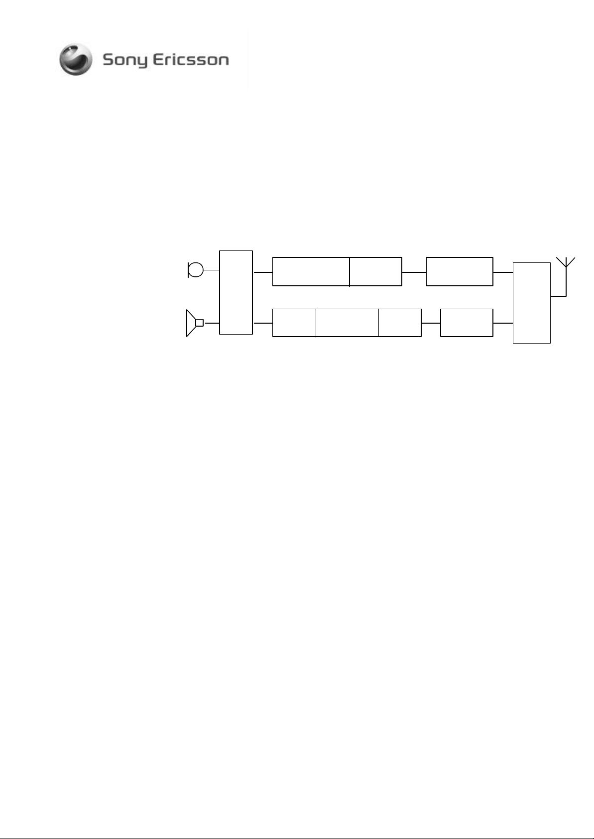
2 OVERVIEW
A general block diagram that describes the GSM phone is shown in the figure
below. It shows the signal flow through the phone, and indicates the different
hardware parts involved in the transmission and reception.
4 (16)
B
A
S
E
B
A
N
All names below the boxes in figure correspond to the project names of the
component that performs the indicated operation.
The component that controls the data flow has the project name MARTHA
and is located in the baseband block. It acts as the Central Processing Unit
containing an AVR microprocessor, DSP, internal RAM and the interfaces to
external components and units as the external memories and the radio. It also
performs the signal processing not done in the other parts.
2.1 THE TX PATH
Modulation, and
channel selection Amplification
INGELA
channel
MixerCoarse
Low Noise
Amplifier
Power
amplification &
PA + Victoria2
Band filtering
Figure 2.1 Block diagram for GSM phone.
TX / RX
switching
Antenna
The speech signal from the microphone is amplified and digitized to a 16 bitPCM signal in HERTA. It is then sliced into 20 ms pieces and thereafter
speech coded in DSP to reduce the bit rate. Further data processing is carried
out in MARTHA that includes channel coding, interleaving, ciphering and
burst formatting. The data is then put through a wave form generator (IQ
signal) before it is fed to the radio.
The RF-ASIC INGELA is the heart of the radio. It has an integrated direct
modulation transmitter where the channel selection and modulation is applied
in one stage via a fractional -N type of synthesizer. The information is added
via the divider ratio of the synthesizer. INGELA also amplifies the signal and
buffers it before it is sent to the power amplifier. The buffer amplifier can be
turn on & off, and it is used to secure pre burs output power. The power
amplifier and VICTORIA 2+ are connected in a control loop that makes the
power ramping, and controls the output power.
Page 5
Prepared (also subject responsible if other) No.
SEM/GUR/BRR Pontus Nelderup 1/1551 - ROA 128 0351/2
Approved Checked Date Rev Reference
SEM/GUR/BRRC Mikael Nilsson 2003-02-28 B
DESCRIPTION
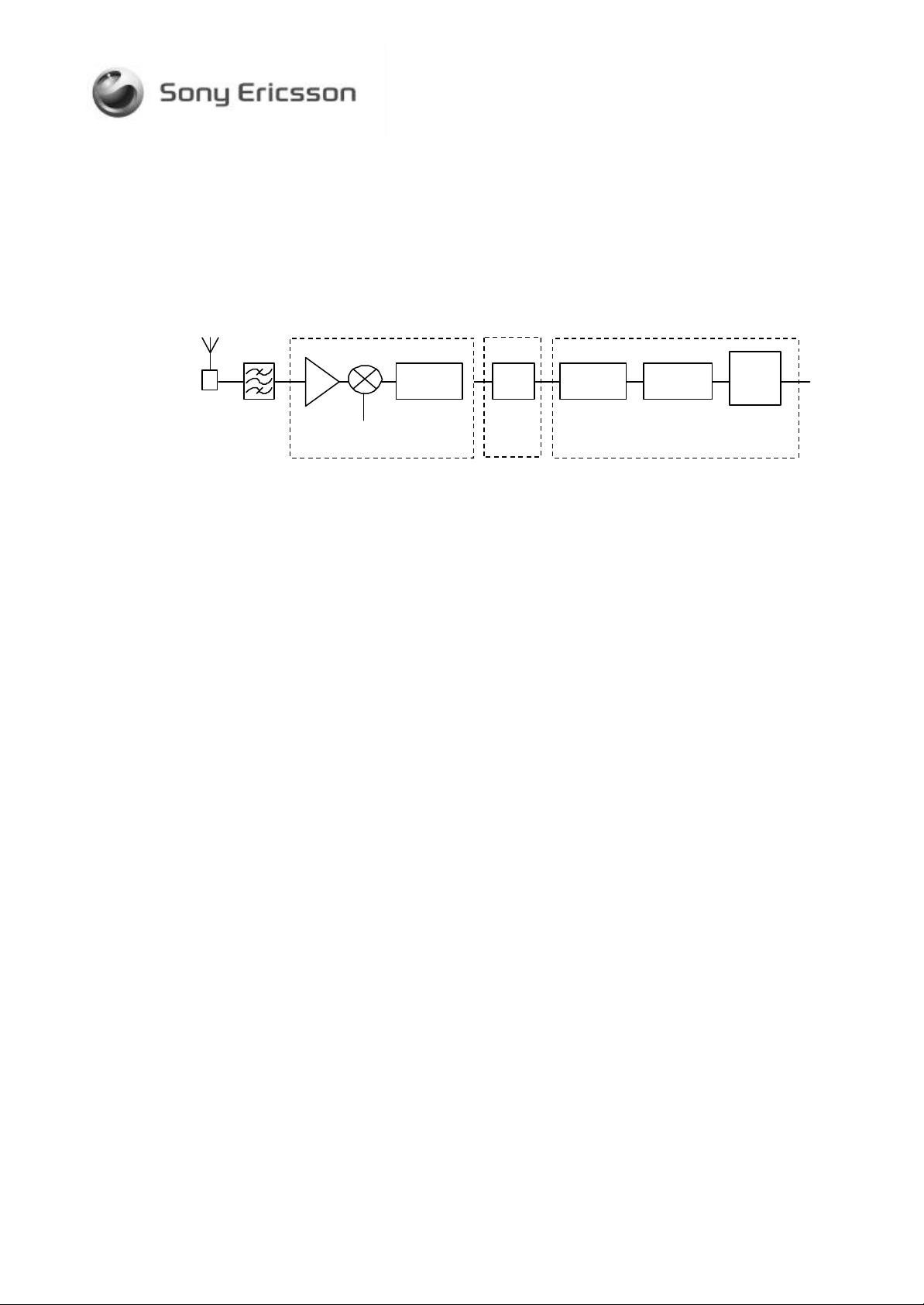
2.2 THE RX PATH
5 (16)
Log-
Polar
Conv.
Ingela
LO
Analog
LP filter
Σ∇
ADC
Digital-
filter
Herta Martha
DC
Comp.
Figure 2.2: Receiver block diagram.
The signal received by the antenna is fed trough a band pass filter and
directly into Ingela. The RX part in Ingela contains a direct conversion
receiver and the RF signal is mixed down to base band in one step. Except
for the RF filter, all filtering except for the anti-aliasing filtering is done in
baseband domain. The main part of channel filtering is in other words done in
the digital domain.
The signals IRA, IRB, QRA and QRB from the radio are hard limited phase
modulated and differential signals that contain all the data received. A fast
phase digitizer in HERTA, demodulates these signals and the phase
information is then fed to MARTHA.
The handling of the DC-level is a big difference compared to the super
heterodyne receiver. (The received signal is mixed with the same frequency
that will give a DC-signal and the signal information) The DC component has
to be removed before detection otherwise the ADC could be saturated, which
would completely destroy the information.
The first step in MARTHA is an equalizer that uses a Viterbi algorithm to
create a model of the channel. Then the received bursts are further processed
to decipher the information. After the de-interleaved (collection and
reassembling all eight “half bursts” into a 456 bit message), the sequence is
decoded to detect and correct errors during the transmission. The decoder
uses soft information (probability that a bit is true) from the equalizer to
improve error correction.
Finally the bit stream is speech decoded in the DSP and then transformed
back into analogue speech in HERTA.
Page 6

Prepared (also subject responsible if other) No.
SEM/GUR/BRR Pontus Nelderup 1/1551 - ROA 128 0351/2
Approved Checked Date Rev Reference
SEM/GUR/BRRC Mikael Nilsson 2003-02-28 B
DESCRIPTION
3 Frequency plan
The PLL in INGELA will be used for both RX and TX operation. Direct
conversion will be used for RX and TX. In TX mode, the PLL will work directly
on the transmitted frequency, whereas the RX VCOs will operate at the
double received frequency. The LO will then be divided by two just before
entering the mixer.
TX-band RX-band
EGSM 880.2-914.8 MHz 925.2-959.8 MHz
DCS 1710.2-1784.8 MHz 1805.2-1879.8 MHz
PCS 1850.2-1909.8 MHz 1930.2-1989.8 MHz
6 (16)
The frequencies that correspond to the channel numbers (ARFCN) for the
different bands are
TX-band (MHz) Channel
numbers
EGSM
DCS
PCS
890 + 0.2⋅n
890 + 0.2⋅(n-1024)
1710.2 + 0.2⋅(n-512) 512 ≤ n ≤ 885
1850.2 + 0.2⋅(n-512) 512 ≤ n ≤ 810
0 ≤ n ≤ 124
975 ≤ n ≤ 1023
RX-band (MHz)
TX-band(n) + 45
TX-band(n) + 95
TX-band(n) + 80
Page 7

Prepared (also subject responsible if other) No.
SEM/GUR/BRR Pontus Nelderup 1/1551 - ROA 128 0351/2
Approved Checked Date Rev Reference
SEM/GUR/BRRC Mikael Nilsson 2003-02-28 B
DESCRIPTION
4 The radio blocks
4.1 The antenna switch
The antenna switch is the block that combines the signals from the power
amplifier (one for EGSM and one for DCS & PCS) going towards the antenna,
with the three signal paths leading towards the RF ASIC INGELA. It is solved
with a PIN diode switch solution in a multilayer module.
7 (16)
TX GSM
TX DCS/PCS
RX GSM
RX DCS
RX PCS
Figure 4.1: Antenna switch PIN diode module.
In transmit mode the main function is to lead the signals from the PA module
to the antenna with as small insertion loss as possible, and in the same time
attenuate power trying to leak between the TX paths and the RX paths.
In receive mode the main function is to lead the small signal picked up by the
antenna with as small insertion loss as possible to the RF filters and then
further towards the low noise amplifiers in INGELA.
The antenna switch module is also contributing to the suppression of
harmonics generated in the PA module, and slightly helping in the attenuation
of high out of band blocking interfering signals that might be picked up by the
antenna since the bandwidth is naturally not infinite.
Page 8

Prepared (also subject responsible if other) No.
SEM/GUR/BRR Pontus Nelderup 1/1551 - ROA 128 0351/2
Approved Checked Date Rev Reference
SEM/GUR/BRRC Mikael Nilsson 2003-02-28 B
DESCRIPTION
4.2 The Receiver
4.2.1 RF filter and balun
An unwanted out-of-band signal might limit the front-end thereby making it
impossible to detect the wanted signal. Possible out of band interfering
signals must therefore be attenuated to the same levels as the in band
blocking requirements for which the front-end circuitry is designed.
Simplified calculations show the maximum allowable attenuation (including
losses in the PCB, mismatch etc) from antenna to LNA input to achieve a
nominal sensitivity of -105 dBm (which is stated in the generic design
specification, the GSM specification states –102dBm):
8 (16)
• E-GSM: 6.4 dB DCS: 6.4 dB PCS: 6.4dB
We have chosen the following specification for balanced SAW filters.
• Insertion loss (dB): Typ: 3.0 Max: 4.0
• Ripple (dB): Typ: 0.5 Max: 1.0
For the antenna switch we have chosen to specify:
• Insertion loss EGS M (dB): Max: 1.2
• I nsertion loss DCS (dB): Max: 1.5
• I nsertion loss PCS (dB): Max: 1.5
4.2.2 Receiver front-end
The RF signal is amplified and then directly converted to a base band signal.
The conversion is done by dividing the signal into I and Q base band signals,
fLO= fRF and the LO signal is 0° in phase at the I channel and in +90° with the
Q channel. The down converted spectrum will be folded around DC. The base
band signals are amplified to a level that is suitable for the ADC.
The primary task of the base band filtering in Ingela is to prevent aliasing in
the ADC. The sample frequency of the Σ ∆ A/D converter is 13 MHz.
Interfering signals and noise with frequencies close to 13 MHz offset (and
multiples of fs) will be folded around f
filter will also reduce the power from adjacent and blocking signals. Limitation
of the noise bandwidth and adjacent channel power is mostly done in the
digital filter chain in Martha.
into the base band. This base band
s/2
Page 9

DESCRIPTION
Prepared (also subject responsible if other) No.
SEM/GUR/BRR Pontus Nelderup 1/1551 - ROA 128 0351/2
Approved Checked Date Rev Reference
SEM/GUR/BRRC Mikael Nilsson 2003-02-28 B
RF DCS
9 (16)
DCS / PCS
GSM
RF PCS
VCO
VCO
RF GSM
0° 90°
90°
0°
Figure 4.2: Receiver front-end.
IR A
IR B
QR A
QR B
4.2.3 VCO
The VCOs are on chip. To meet the demands on LO phase noise we need a
high Q-value in the resonator circuit.
High Q coil resonators make it possible to fulfi ll the requirement on phase
noise, -140 dBc/Hz at 3 MHz offset from the carrier, and at the same time
achieve as large tuning range as possible.
Page 10

Prepared (also subject responsible if other) No.
SEM/GUR/BRR Pontus Nelderup 1/1551 - ROA 128 0351/2
Approved Checked Date Rev Reference
SEM/GUR/BRRC Mikael Nilsson 2003-02-28 B
DESCRIPTION
4.2.4 Sigma delta A/D Converter
The base band signals are digitized with a dual Σ ∆ A/D converter. Each
output is a 13 MHz bit stream. The conversion generates high frequency
quantization noise that must be attenuated in the digital filter.
MCLK input level: > 0.4 Vpp, and < 1.2 Vpp.
Dynamic range: 70 dB (20*log(1.54/0.487E-3)).
Min SNR: 12 dB
Input level range: 487 µVpp-1.54 Vpp (differential)
10 (16)
4.2.5 Digital filter
Almost all of the channel- and adjacent channel filtering is done in digital
filters.
I and Q data are serially sent from the ADC. The first filter has to reduce the
noise from the Σ ∆ to avoid noise being folded down to base band.
Figure 4.3: Sigma delta A/D converter in Herta.
Page 11

VTUNE
PS
PHDOUT
MOD[A-D]
Delay
Pump
HIGH
LOW
DESCRIPTION
Prepared (also subject responsible if other) No.
SEM/GUR/BRR Pontus Nelderup 1/1551 - ROA 128 0351/2
Approved Checked Date Rev Reference
SEM/GUR/BRRC Mikael Nilsson 2003-02-28 B
4.3 The transmitter
4.3.1 Frequency synthesis and modulation
The “frequency synthesis and modulation” block is almost completely
integrated in the RF ASIC Ingela. The loop filter is external and the
modulation parts are integrated in the base band ASIC Martha.
11 (16)
MARTHA
∆Σ
INGELA
XO
Prescaler
To receiver
block
Phase
Detector
TX-VCO
TX-VCO
RX-VCO
RX-VCO
Charge
Loop filter
To PA
block
Figure 4.4: Block schematic of the frequency synthesis and modulation.
Page 12

Prepared (also subject responsible if other) No.
SEM/GUR/BRR Pontus Nelderup 1/1551 - ROA 128 0351/2
Approved Checked Date Rev Reference
SEM/GUR/BRRC Mikael Nilsson 2003-02-28 B
DESCRIPTION
4.3.2 Direct modulation and frequency synthesis
The main component for the frequency synthesis and up-conversion is Ingela.
The direct modulation concept will be used and the base-band chip Martha
has, together with Ingela, all the required functions for direct modulation. The
use of direct modulation means that we will not have any intermediate
frequency (IF) in the transmitter chain.
To be able to keep the VCO gain at a reasonable level, four different VCOs
are implemented: High band/RX, High band/TX, Low band/RX and Low
band/TX. These VCOs are totally integrated in Ingela. The logic signals
RXON, TXON and BSEL are used to determine which VCO should be used.
12 (16)
The modulation and (partly) the channel selection is performed in a Σ ∆
modulator in Martha, which controls the divide ratio in a fractional-N PLL in
Ingela via four parallel 26 MHz leads.
Other information that needs to be sent to Ingela, such as charge pump
current setting and divide ratio offset, is transferred via the serial bus,
SYNCLK, SYNDAT, SYNSTR.
Figure 4.4 shows a block schematic for the frequency and modulation block.
4.3.3 Phase detector
The reference frequency from the crystal oscillator (XO) is 13MHz and is not
divided down before entering the phase detector. The phase detector is
implemented to be able to trig on both up going and down going flanks, so the
comparison frequency is twice the reference frequency, i.e. 26MHz.
4.3.4 Prescaler
The prescaler divides the VCO signal down to 26MHz, which is the
comparison frequency in the phase detector. An offset value, N0, is sent to the
prescaler via the Ingela F-word on the serial bus. N0 is programmable in
integers between 16 and 95, which means the frequency can be chosen in
steps of 26MHz by only using N0. To be able to select channels with 200kHz
spacing, the prescaler divide ratio, N, can be varied by MOD[A-D] from the
output of the Σ ∆ in Martha. MOD[A-D] are parallel logic signals that can
change state at the rate of 26MHz. If we call the contribution from MOD[A -D]
N
, the actual instant divide ratio, N, is given by
mod
Page 13

[
]
[
]
Prepared (also subject responsible if other) No.
SEM/GUR/BRR Pontus Nelderup 1/1551 - ROA 128 0351/2
Approved Checked Date Rev Reference
SEM/GUR/BRRC Mikael Nilsson 2003-02-28 B
DESCRIPTION
NNN += ,
mod0
95,,160K∈N ,
mod
Since the loop will be chosen to be much slower than the frequency of
changing N, the effect will be that a stable carrier is generated at a frequency
that corresponds to the average value of N. In our implementation, N
limited to the range [0,…,12].
The channel selection is performed by first choosing an appropriate value of
N0 and then controlling C, the input value to the Σ ∆ modulator. The generated
(un-modulated) carrier is described by the equation
36
HzCNf
00
1051026)6( ⋅⋅+⋅⋅+=
15,,0
K∈N
mod
13 (16)
is
where C is an integer in the range [-8840,…,8840].
The modulation is up-sampled several times and filtered in the waveform
generator (WFG) before coming in to the Σ ∆ modulator. Thus, the output from
the Σ ∆, N
, consists of information from both channel selection and
mod
modulation. The loop bandwidth has to be chosen so wide (≈200kHz) that the
modulation information passes through.
4.3.5 Charge pump and pulse skip detector
The charge pump current is programmable with I
makes it possible to tune the loop bandwidth, which is desirable especially
due to the matching that needs to be made between the pre filtering of the
information, that is performed in the waveform generator (WFG), and the loop.
Since the VCO gain will vary over the frequency band, with different units and
over temperature, this match ing has to be made by calibration in production
and a temperature compensation table.
4.3.6 Loop filter
in the Ingela F-word. This
phd
The loop filter is the only thing in the PLL that is implemented with discrete
components. Since the Σ∆ modulator is of the order three, we need a fourth
order loop filter to get a frequency roll off that is good enough.
Page 14

Power
Tx
DCS/PCS
Band
DCS/
Prepared (also subject responsible if other) No.
SEM/GUR/BRR Pontus Nelderup 1/1551 - ROA 128 0351/2
Approved Checked Date Rev Reference
SEM/GUR/BRRC Mikael Nilsson 2003-02-28 B
DESCRIPTION
4.4 Power amplifier & Power control block:
The block consists of the power control and power management ASIC
Victoria 2+ and one power amplifier from Skyworks which include an amplifier
for the GSM band and one for the combined DCS/PCS band. The output
power is controlled by adjusting the power amplifier current, which is
measured via a 0.051 Ω resistor. The RF output power from Ingela consists of
two balanced signals, TXOLA and TXOLB TXOH for GSM and TXOHA and
TXOHB for DCS/PCS. These balanced signals are converted to singe ended
signals in two baluns and fed to two PI-network attenuators before they are
fed to the power amplifiers.
14 (16)
To change band, two twin transistor switches are used to switch the Vapc
signal to either the GSM or DCS/PCS PA. As control signal for these
transistors, BSEL0 is used.
For maximum freedom an additional low pass filter is inserted between
Victoria2 and the power amplifiers in the PAREG node.
V
Powlev
Batt
Control
GSM
Bsel0
GSM PA
Select
PCS
PA
TxON
frontend
Pctl
Figure 4.5. Overview of the PA and PA-control block.
Page 15

Prepared (also subject responsible if other) No.
SEM/GUR/BRR Pontus Nelderup 1/1551 - ROA 128 0351/2
Approved Checked Date Rev Reference
SEM/GUR/BRRC Mikael Nilsson 2003-02-28 B
DESCRIPTION
4.5 The Voltage Controlled X-tal Oscillator (VCXO):
The voltage controlled crystal (xtal) oscillator (VCXO) is an oscillator consists
of two main components: an active device that acts as an amplifier and a
feedback network to provide positive feedback in the system. The feedback
network is frequency sensitive and includes some types of resonators to set
the operating frequency. In addition some type of variable reactance element
must be present for control the frequency. Normally the variable reactance is
controlled by a dc voltage, hence the term voltage – controlled oscillator .The
typical design emphasis is on low noise stability bandwidth, linear and
wideband tunability, reliability and low cost.
15 (16)
The solution is an internal Pierce oscillator in Ingela using an external crystal.
The13 MHz signal is the reference for the different frequency generator in the
radio and also the clock signal for the logic circuits. This requires a very
frequency stable 13 MHz generator. That is the reason for using crystal
oscillator.
4.6 Power Management
The radio is supplied using an external low -noise voltage regulator in order to
have a very clean voltage suppl y that is necessary to avoid noise or
interference especially for the VCOs integrated in Ingela.
4.7 Bluetooth
The Bluetooth function of the phone is implemented in the baseband ASIC
Irma B and the RF Bluetooth module Ran. All of the Bluetooth radio is inside
the module except for a filter that is placed between the module and the
antenna. The reason to include this filter is to improve the isolation between
the GSM bands and the Bluetooth band to not have degraded sensitivity in
Bluetooth while transmitting in the other bands.
Page 16

Prepared (also subject responsible if other) No.
SEM/GUR/BRR Pontus Nelderup 1/1551 - ROA 128 0351/2
Approved Checked Date Rev Reference
SEM/GUR/BRRC Mikael Nilsson 2003-02-28 B
DESCRIPTION
5 PRINTED CIRCUIT BOARD
The printed circuit board is an 8-layer board. Five layers (layer 1, 2, 3, 7 & 8)
carry all the connections between component terminals. Two layers (layer 4 &
6) are used as ground planes, and both these planes co ver the whole board.
The layer between the ground planes (layer 5) is made to carry sensitive
signals and strip lines.
The layer structure is listed below:
Layer 1 Components, radio signals (Primary side)
16 (16)
Layer 2 Radio and base band signals
Layer 3 Radio and base band signals
Layer 4 Ground plane
Layer 5 Radio strip line layer
Layer 6 Ground plane
Layer 7 Base band and Bluetooth signals
Layer 8 Components, base band and Bluetooth signals (Secondary side)
 Loading...