Sony Ericsson K850 Schematics
ABOUT
SEMC Troubleshooting Manual
Troubleshooting Manual
K850
K850
ABOUT TROUBLESHOOTING MEASUREME NT POINTS
1203-2528 rev. 1
APPENDIXCOMPONENT OVERVIEW FUNCTIONAL OVE R VIEW
1 (101)

ABOUT
Con tents
SEMC Troubleshooting Manual
K850
ABOUT
General information
The purpose of this document is to provide enhanced technical information for Sony Ericsson
repair technicians in order to assist during service, repair and troubleshooting operations on Sony
Ericsson mobile phones. It should be used as a complement to other repair instructions and tools
as notifi ed by the local Sony Ericsson representative.
To search for components throughout the entire document use the “search” function in Adobe
Acrobat Reader 7.0 (or later version) and enter the component name or other word. Use zoom to
enlarge.
For easier navigation of the document you can use the bookmarks that appear in the Bookmarks
tab on the left side of the Adobe Acrobat Reader window. Each bookmark jumps to a page in the
document.
Disclaimer
This document is Sony Ericsson confi dential and should be treated as confi dential in accordance
with the agreement with Sony Ericsson. This document is intended for use by authorized service
technicians only. Sony Ericsson is not to be held responsible for any damages or losses caused
intentionally or unintentionally due to unauthorised use of the information in this document.
Revision History
Rev. Date Changes / Comments
1 2/14/2008 Initital revision.
ABOUT 2
Contents 2
TROUBLESHOOTING 3
Equipment List 3
On/Off Problems 8
Flash Problems 8
Dead Phone Problems 9
Display Problems 9
Display Illumination Problems 10
Key Problems 10
LED Problems 11
Main Camera Problems 11
VGA Camera Problems 12
Camera Door Problems 12
Vibrator Problems 13
Charging Problems 13
USB/VBUS Charging Problems 14
SIM Problems 14
Memory Stick Problems 15
Audio Internal Problems 15
Audio External Problems 16
FM Radio Problems 16
Bluetooth Problems 17
GSM Network Problems 18
WCDMA Network Problems 18
Xenon Flash Problems 19
System Connector Protection Test 20
Current Comsumption Test 20
Battery & Current Calibration Test 22
Backup Capacitor Test 22
Test Charging 23
ASIC Revision Test 23
Reference Measurement Points 24
TEST POINTS 25
Front Side 25
Back Side 26
SIM & Memory Card Holder 27
Sofi a Top Schematic 28
Application & System Performance Top 29
System Top 30
System Control - Clocks & Resets 31
System Memories 32
Power Top 33
Power Regulators & Charging 34
Power Camera 35
Power ASICs 36
Power Memories 37
Connectivity Top 38
Connectivity ADC & I2C 39
Connectivity Cards 40
Connectivity Connectivity 41
Connectivity Keypad 42
Connectivity Camera Door & Flash 43
Access Top 44
Access - GSM & UMTS 45
Access - Bluetooth 46
Imaging Top 47
Imaging Display 48
Imaging Camera 49
Imaging LMU 50
Audio Top 51
Audio Analog 52
Audio Digital 53
FM Radio 54
Test 55
Thor RF Module Top 56
Thor RF Module GSM/EDGE Tx + FEM 57
Thor RF Module GSM/EDGE Rx + Synth 58
COMPONENT OVERVIEW 59
Front Side B - X 59
Back Side C - E 60
Back Side L - Z 61
FUNCTIONAL OVERVIEW 62
Technical Description 62
Block Diagram Access 71
Block Diagram Application 72
Power Distribution & Clocking Concept 73
APPENDIX 74
Replaceable Parts 74
Components B2101 - D2000 75
Components D2010 - D2105 - D2404 76
Components D2420 - D2460 77
Components L2200 - L2401-04 - N1200 78
Components N1210 - N1400 79
Components N2000 - N2201 80
Components N2202 - N2203 81
Components N2205 - N2208 82
Components N2400 - N2402 - N2500 83
Components N2525 - N3100 - N3101 84
Components N4101 - N4200 85
Components S2400 - S2402 - S2403 86
Components V2202 - V2402 - V2405 86
Components V2420-21 - V2425 - V2428 87
Components V2477-78 - V2500 87
Components X1200 - X1201-03 - X2200 88
Components X2409 - X4300 - X2410 89
Components X2511 - X3105 89
Components X4301 90
Camera Module 5 MPixel 90
VGA Camera 90
Xenon Flash Assembly 91
Display 91
Keyboard Schematics 92
Troubleshooting Software Documentation 93
Troubleshooting Fixture Setup Guide 100
ABOUT
1203-2528 rev. 1
2 (101)

TROUBLESHOOTING
Equip ment List
SEMC Troubleshooting Manual
K850
K850 Equipment List
Note: More additional information about the equipment used for TRS can be found in Repair
Tools Catalogue on CSPN or on the following location: CSPN – Repair Instructions – Electrical –
K850 – Equipment List.
TRS Fixture Kit
Location: CSPN-Repair Instructions-Electrical-K850-Equipment List
Dummy Battery
Location: CSPN-Repair Instructions-Electrical-K850-Equipment List
Part number: 1200-0725
Instruments
Power Supply Channel 1 VBATT
Agilent 6632B or similar
Location: CSPN-Repair Instructions-Level: Mechanical-Tool Catalogue
Instrument Settings:
Voltage: 3.8 Volt
Limiter: 2A
Note: During the calibration the accurate voltage from the VBATT must be within ±0.015 V. If this
is not fulfilled it will result in a faulty calibration. (For more information about recommended power
supply units, see the Repair Tool Catalogue on CSPN under the Mechanical level. The Power
Supply Channel 1 VBATT must allow reverse current.
Note: Maximal cable length between the Power Supply Channel 1 VBATT and the dummy
battery must not exceed 1m. The cable must have a capacity for at least 16A.
Digital Multimeter (DMM)
Fluke 83 or similar
Location: CSPN-Repair Instructions-Level: Mechanical-Tool Catalogue
Spectrum Analyzer
HP 8595E or similar
Location: CSPN-Repair Instructions-Level: Mechanical-Tool Catalogue
RF probe
HP 85024A or similar
Location: CSPN-Repair Instructions-Level: Mechanical-Tool Catalogue
Mobile Phone Tester
Yokogawa VC230 or similar
Location: CSPN-Repair Instructions-Level: Mechanical-Tool Catalogue
FM Signal Generator
Agilent E4433B or similar
Location: -
RF Connectors
Adaptor 33 N-BNC-50-1
Adaptor to Signal Generator RF Output
Se Picture 1
Location: -
Picture 1
TROUBLESHOOTING
Note: It is very important to follow instrument settings instructions when performing the Battery
Calibration Test.
Power Supply Channel 2 DCIO/SEPI
Agilent 6632B or similar
Location: CSPN-Repair Instructions-Level: Mechanical-Tool Catalogue
Instrument Settings:
Voltage: 5.0 Volt
Limiter: 2A
Note: It is very important to follow instrument setting instructions when performing the Current
Calibration Test.
Oscilloscope
Tektronix TDS 2012 or similar
Location: CSPN-Repair Instructions-Level: Mechanical-Tool Catalogue
PC Package & PC Software
PC Package (Computer)
Location: CSPN-Repair Instructions-Level: Mechanical-Tool Catalogue
1203-2528 rev. 1
3 (101)

TROUBLESHOOTING
Equipment List
SEMC Troubleshooting Manual
K850
Urquell Fault Trace SW with project file
Location: CSPN-Repair Instructions-Electrical-Trouble Shooting Application
Project File: K850Project_R1A
Drivers
SEPI BOX Drivers
Location: EMMA III-Drivers-SEPI
SE Communication Interface SEPI BOX
Location: CSPN-Repair Instructions-Level: Mechanical-Tool Catalogue
Part number: LTN 214 1484
Se Picture 2.
Picture 2
RF Test Cable Flexible
Location: CSPN-Repair Instructions-Level: Mechanical-Tool Catalogue
Part number: RPM 119 885
Se Picture 4.
Picture 4
SEPI Interface Cable
Location: CSPN-Repair Instructions-Level: Mechanical-Tool Catalogue
Part number: KRY 101 1119/1
Se Picture 5.
– A1
TROUBLESHOOTING
Cables
USB Computer Cable
Location: CSPN-Repair Instructions-Level: Mechanical-Tool Catalogue
Se Picture 3.
Picture 3
DSU-60/USB Cable
Location: CSPN-Repair Instructions-Level: Mechanical-Tool Catalogue
Part number: KRY 101 1413
Picture 5
Power Cable RED to Power Supply Channel 1 VBATT
Maximum Length: 1m
Location: CSPN-Repair Instructions-Level: Mechanical-Tool Catalogue
Power Cable BLACK to Power Supply Channel 1 VBATT
Maximum Length: 1m
Location: CSPN-Repair Instructions-Level: Mechanical-Tool Catalogue
Customized Power Supply Channel 2 DCIO/SEPI Cable
To perform Current Calibration the phone must be supplied directly through the system connector.
Customize the cable according to following instructions:
1203-2528 rev. 1
4 (101)
TROUBLESHOOTING
Equipment List
SEMC Troubleshooting Manual
K850
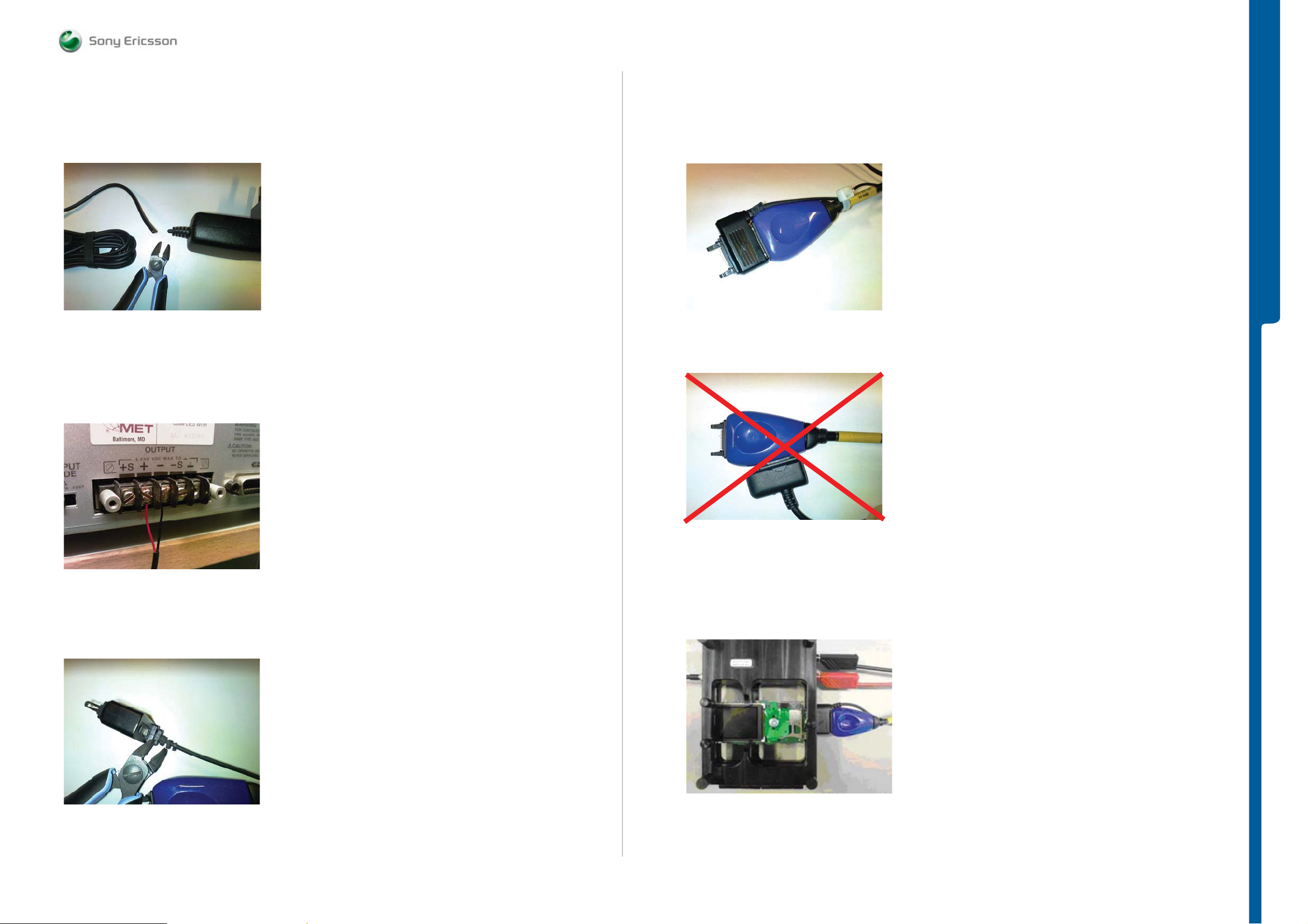
STEP 1:
Take the CST-75 battery charger and cut of the charger according to Picture 6.
Picture 6
Note: Cable length must be exact 1.3m.
STEP 2:
Connect the CST-75 charger Red or White wire to the Plus Output and the Black wire to the
Minus (GND) Output at Power Supply Channel 2 DCIO/SEPI according to Picture 7.
Picture 7
STEP 4:
Connect DCIO and SEPI Interface Cable – A1 cables according to Picture 9.
Picture 9
TROUBLESHOOTING
The setup in Picture 10 is WRONG!
Picture 10
STEP 3:
Trim the flex protection material from inside of the charger plug according to Picture 8.
Picture 8
Power Supply Channel 2 DCIO/SEPI Cable Connection Setups
Correct DCIO/SEPI Cable setup when TRS Fixture is used.
Picture 11
Note: Example of DCIO/SEPI and K750 TRS Fixture Setup.
1203-2528 rev. 1
5 (101)
TROUBLESHOOTING
Equipment List
SEMC Troubleshooting Manual
K850
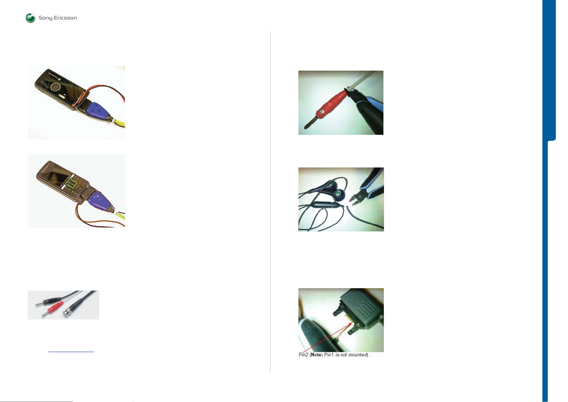
Correct DCIO/SEPI Cable setup without the TRS Fixture.
Picture 12
Picture 13
STEP 2:
Cut the Red lab plug according to Picture 15
Picture 15
TROUBLESHOOTING
STEP 3:
Use any Hands free (PHF) Cable and cut according to Picture 16
Picture 16
Customized FM Radio Cable
STEP 1:
Use Cable according to Picture 14
Picture 14
Product Name: Test lead BNC-4mm 1,5m
Product Description: Test lead with 4 mm lab plugs at one end and a BNC plug at the other.
Manufacturer: PMK Germany
Location: http://www.elfa.se/en/
Part number: 46-310-40 (Note: This is ELFA part number)
or other supplier.
Note: Minimum Cable length 40 cm.
STEP 4:
Use only wire connected to Pin2 and cut all rest wires according to Picture 17.
Use digital multimeter instrument (DMM) and perform diode measurement to select wire
connected to Pin2 at hands free system connector plug.
Picture 17
1203-2528 rev. 1
6 (101)
TROUBLESHOOTING
Equipment List
SEMC Troubleshooting Manual
K850
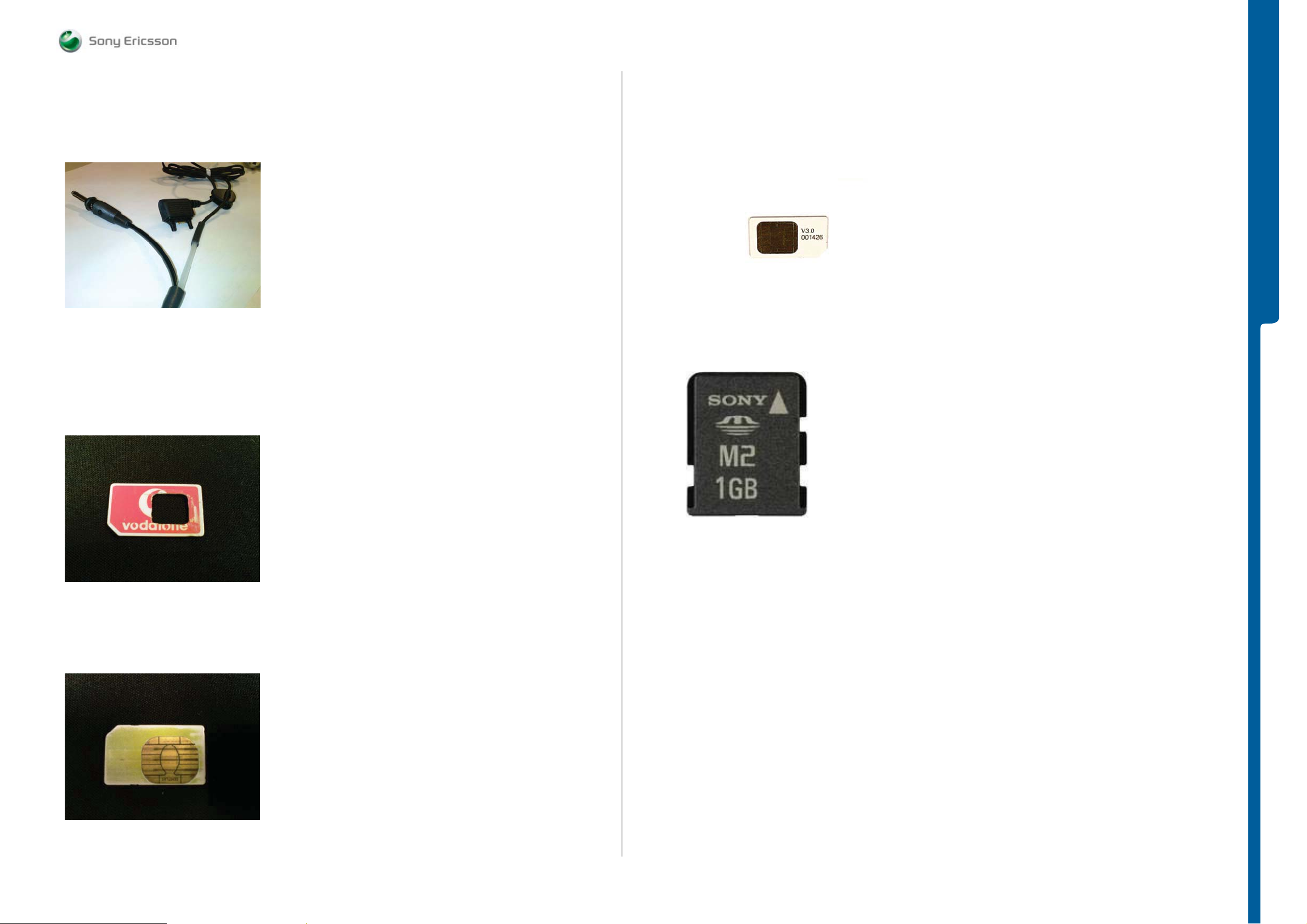
STEP 5:
Connect by soldering cable from Picture 15 and cable from Picture 17 according to Picture 18.
Picture 18
Test Cards
Dummy SIM
Customize SIM Card according to Picture 19.
Picture 19
Test SIM GSM/UMTS
One Test SIM GSM/UMTS is needed to perform Current Consumption Test, se Picture 21.
Location: To buy a Test SIM GSM/UMTS, please contact your supplier of test equipment.
Picture 21
TROUBLESHOOTING
Sony Memory Stick Micro Card M2
Any functional Memory Stick Micro M2 Card, se Picture 22
Picture 22
Local SIM
Any functional Local SIM Card, se Picture 20
Picture 20
1203-2528 rev. 1
7 (101)
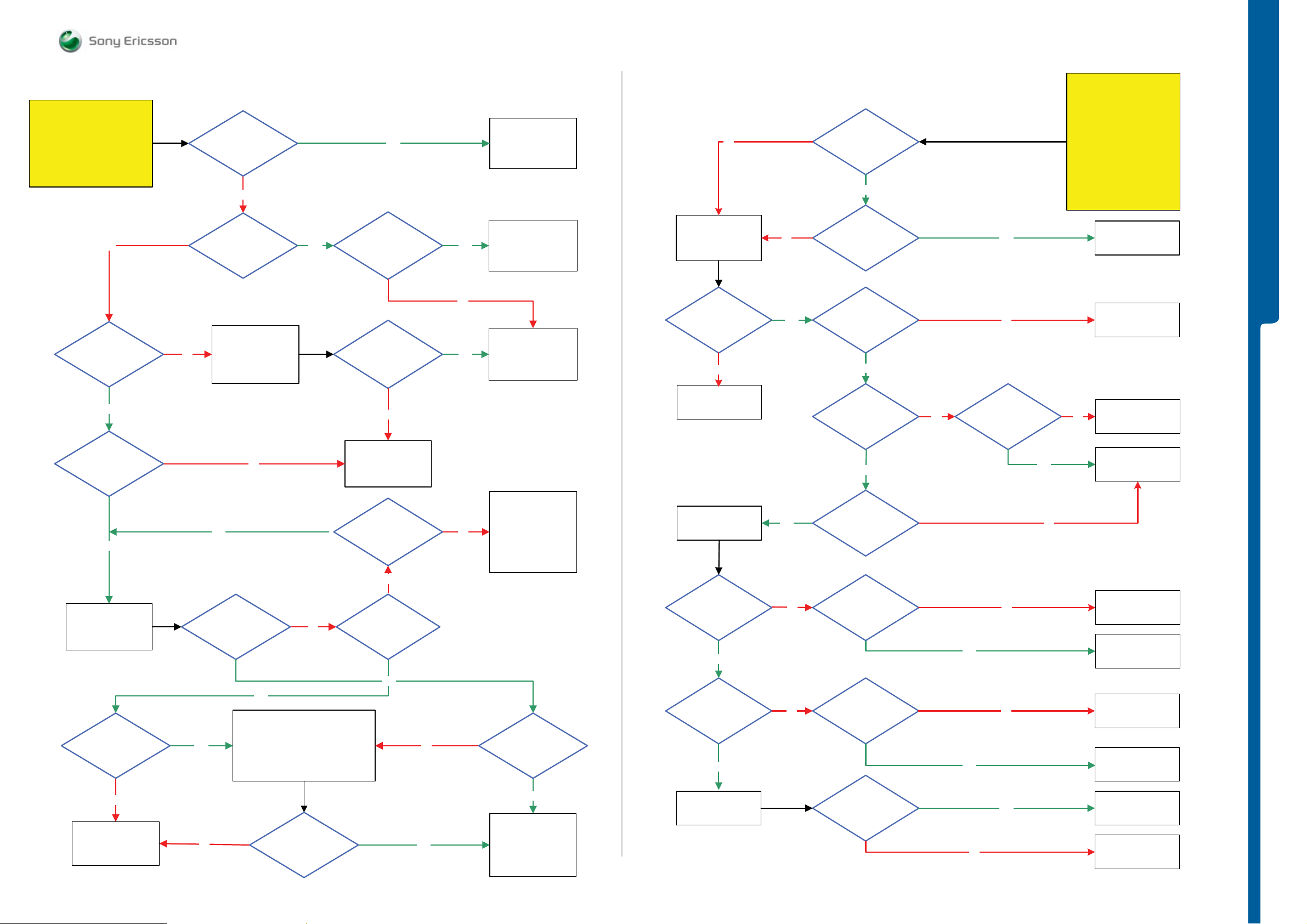
TROUBLESHOOTING On/Off Problems
/ Flash Problems
SEMC Troubleshooting Manual
K850
START
Connect:
Dummy Battery connected
to VBATT
No
Is the
phone consuming
any current when
powering on the
phone
Yes
On/Off problems
Is the phone
consuming more than
1mA when the phone
is powered off
No
Is it possible to
power on the phone
Connect a chargerNo
Yes
Yes
Is it possible to power
off the phone
Is the phones
behavior as normal
Optimized
charging
No
Yes
No
Yes
Go to
Dead phone
Problems part 1
Go to
Current
Consumption Test
After this go to
Charging Test.
Go to
Key problems
No
Power up the phone
Connect USB Cable
From PC
The phone
indicate charging
on display
No
Go to
USB/VBUS Charging
problems
No
Yes
Flash problems
Flash process
Start-up
When using
EMMA
Yes
Download
ITP SW
By using EMMA
Passed
5 Volt DC at
MP 123 (C2414)
Yes
3.3 Volt DC
Pulses at
MP 120 (C2476)
No
Yes
No
1.8 Volt DC
Pulses at
MP 23 (R2427)
START
Step 1:
Perform System
Connector Protection Test.
Try to Flash the phone by
No
Step 2:
Phone with Normal SW
Use TRS Fixture
Connect:
Display and Keypad
Connect: VBATT
using EMMA III SW
SL 5 Replace
D2010
SL 4 Scrap
SL 5 Replace
R2484
SL 4 Scrap
SL 5 Replace
D2000
SL 4 Scrap
TROUBLESHOOTING
Is the current
consumption between
10mA and 70mA
Yes
Flash
the phone with
correct CDA
software
Flash
the phone with
ITP software
successful
No
Yes
CDA Software
Flash
Successful
Yes
1. Customize the phone into DPY/Z
2. Startup the phone and wait for
the configuration to take place
(takes less than a minute)
3. Customize with correct CDA
4. Activate the phone
No
Go to
Dead Phone
Problems part 1
Press
2 and 5
Connect USB
Run Pre-config 1 and 2
Run DPY/Z
Successful
Flash
No
Flash process
started
Yes
Replace
D2404
No
Go to
System Connector
Protection Test.
Disconnect the
phone from
TRS Fixture
Yes
Yes
1.8 Volt DC
Pulses at
MP 125 (C2474)
Yes
No
After this go to
Flash problems
Max 2 Ohm between
MP 119 (X2400_Pin11)
and MP 117
(Z2450 pin 3)
Yes
Max 2 Ohm between
MP 118 (X2400_Pin10)
and MP 116
(Z2450 pin 4)
NoYes
Problem
solved
Yes
No
No
Max 0.5 Ohm between
MP 119 (X2400_Pin11)
and MP 121
(Z2450 pin 2)
Max 0.5 Ohm
between
MP 118 (X2400_Pin10)
and MP 122
(Z2450 pin 1)
No
Yes
No
Yes
Replace
System Connector
X2400
SL 5 Replace
Z2450
SL 4 Scrap
Replace
System Connector
X2400
SL 5 Replace
Z2450
SL 4 Scrap
No
Go to
Flash problems
No
Problem
solved
Yes
Yes
Claim for a
SW Upgrade
Replace
D2404
Problem
solved
No
Yes
Claim
D2404
SL 5 Replace
D2000
SL 4 Scrap
1203-2528 rev. 1
8 (101)
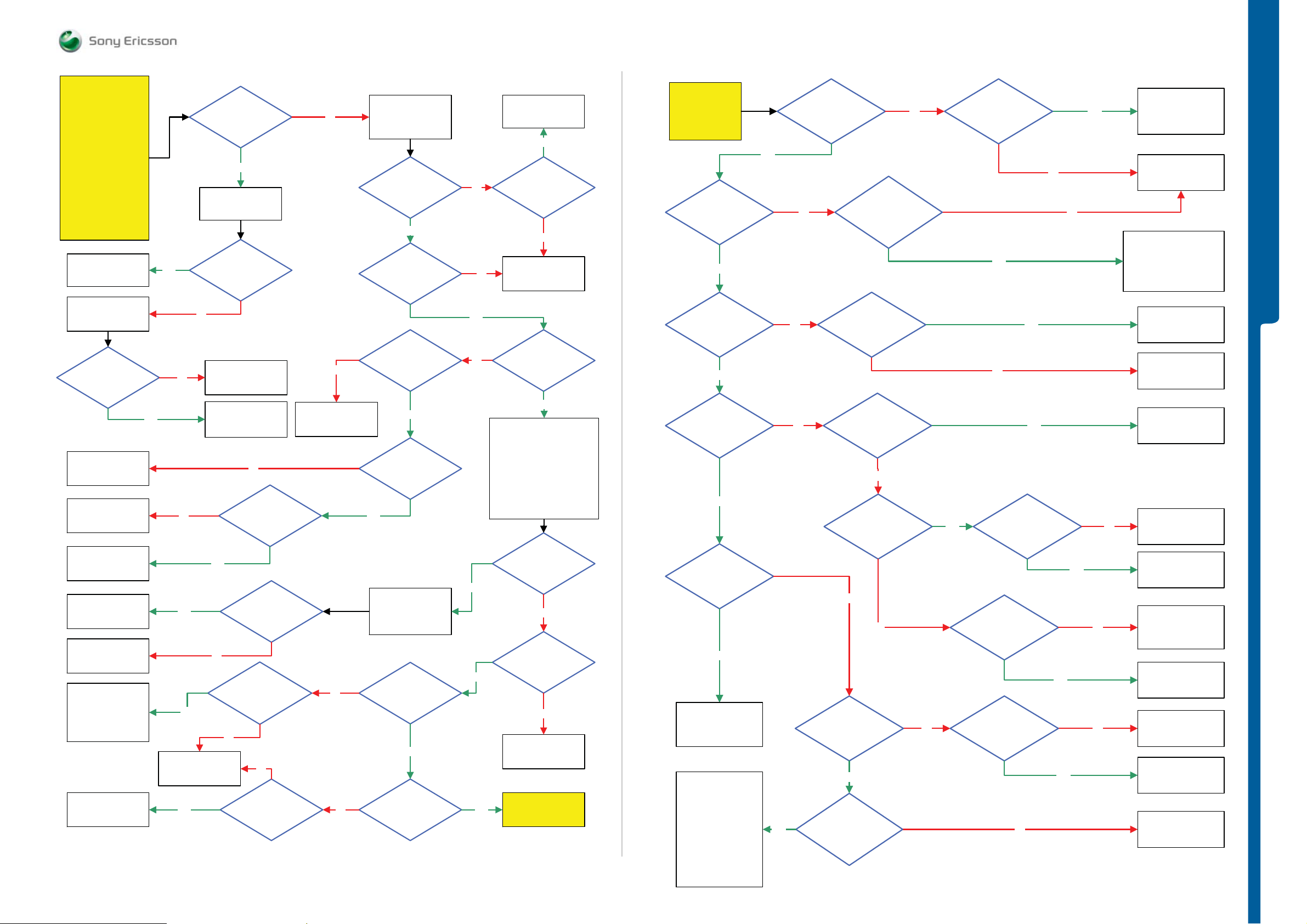
TROUBLESHOOTING Dead Phone Problems
SEMC Troubleshooting Manual
K850
START
Step 1:
Try to recover the phone
using EMMA III SW
Press key 2 and 5
Connect USB Cable
Run pre-config 1 or 2
Run DPY/Z
Step 2:
Use TRS Fixture
Connect VBATT
NOTE:
Do NOT use
DCIO/SEPI Cable!
Replace
N1002, N1200 or
N1210
SL 5 Remove
N2000
SL 4 Scrap
Using more than
1 mA
current
SL 5 Replace
N2000
SL 4 Scrap
Replace
N1200
SL 5 Replace
D2000
SL 4 Scrap
SL 5 Replace
D2010
SL4 Scrap
Go to
Flash Problems
SL 4 Replace
N2400 or V2405
SL 5 Replace
C2400, C2430,
C4213, C3135 or
C3136
SL 5 Replace
Faulty Component
SL 4 Scrap
Yes
Yes
No
No
Yes
Yes
SL 5 Replace
N2000
SL 4 Scrap
Yes
S2400
not pressed
Using more than
1 mA
current
Yes
Try to trace the
faulty component
with freezing spray
N1002
(inside N1200)
N1200, N1210
getting hot
No
SL 5 Replace
N2000
SL 4 Scrap
Try to trace the
faulty component
with freezing spray
MP 149 (R2100)
Yes
Flash process
No
V2405, N2400
C2400, C2430,C4213,
C3135,C3136
Short circuit
No
C2326, C2327,
C2328, C2329, C2330,
C2353, D2000,C2352
Dead Phone problems part 1
No
DCIO/SEPI Cable
MP 6 (B2101 Pin7)
Between Power
No
SL 5 Replace
R2200
SL 4 Scrap
No
26 MHz
MCLK at
successful
No
No
Short circuit
Supply GND and
MP 9 (ST2208 VDDE)
MP 12 (ST2215
Yes
by downloading
Keep S2400
pressed or
connect
32 kHz
RTCCLK at
Yes
32 kHz
RTCCLK at
MP 21 (R2125)
0 Volt
PBA GND
Yes
1.8V DC at
2.8V DC at
VccA)
Try to recover
the phone
ITP SW
AUDIO26
Voltage
Ok
Yes
VANA25
Voltage
Ok
Replace
B2101
No
No
Yes
No
2.6V MP 17 (ST2204 AUDIO26)
2.5V MP 11 (ST2203 VANA25)
2.7V MP 14 (ST2212 VBT27)
2.7V MP 34 (ST2213 VDIG)
2.6V MP 36 (ST2214 VBEAR26)
1.8V MP 158 (ST2217 VCORE18)
1.2V MP 56 (ST2206 VCORE12)
Yes
Yes
YesNo
2.2 Volt at
MP 7 (C2218 VDD_LP)
SL 5 Replace
N2000
SL 4 Scrap
26 MHz
MCLK at
MP 85 (C2116)
Check the following voltages:
All voltages
Current
consumption more
than 50mA
SL 5 Replace
N2000
SL 4 Scrap
Dead Phone
problems part 2
Yes
No
Yes
Ok
No
No
Go to
Dead Phone
problems
Part 2
VDIG
Voltage
Ok
Yes
VBEAR26
Voltage
Ok
Yes
VCORE18
Voltage
Ok
Yes
VCORE12
Voltage
Ok
Yes
Try to Recover the
Phone by
downloading
ITP SW
SL 5 Check
C2301 to C2305,
C2307,C2308,C2311,
C2313 to C2319
C2322,C2324,C2325
D2000
SL 5 replace
Faulty component
and L2200
Yes
Yes
No
No
No
VBT27
Voltage
Ok
D2405,C2402
D2460,C2525,C2524,
N2525,C1407,N1400
Short circuit
C3152
Short circuit
D2000,
D2010,V2231,
C2342 to C2351
Short circuit
1.8 Volt DC at
MP 157 (N2202 Pin1)
No
1.2 Volt DC at
MP 24 (V2207)
Yes
MP 56 (ST2206)
Short circuit
To PBA GND
Dead Phone problems part 2
No
C2470
No
No
No
N1400, C1409
Short circuit
Yes
No
Yes
3.8 Volt DC at
MP 161 (N2202 Pin6)
3.8 Volt DC at
MP 57 (L2201)
C2243
Short circuit
No
Yes
Yes
No
Yes
Yes
No
Yes
Yes
No
No
SL 4 Replace
SL 5 Replace
SL 5 Replace
SL 4 Scrap
SL 4 Replace
D2460, N2525 or
SL 5 Replace
C2470, D2405, C2402,
C2525, C2524 or C1407
SL 5 Replace
SL 4 Scrap
SL 5 Replace
SL 4 Scrap
SL 5 Replace
Faulty component
SL 4 Scrap
SL 5 Replace
No
SL 4 Scrap
SL 5 Replace
C2243 and L2203
SL 4 Scrap
SL 5 Replace
R2207, C2239
and N2202
SL 4 Scrap
SL 5 Replace
SL 4 Scrap
SL 5 Replace
SL 4 Scrap
N1400
C1409
N2000
TROUBLESHOOTING
N1400
C3152
N2000
L2203
Replace
N2202
L2201
N2000
Replace
L2200
SL 4 Scrap
1203-2528 rev. 1
9 (101)
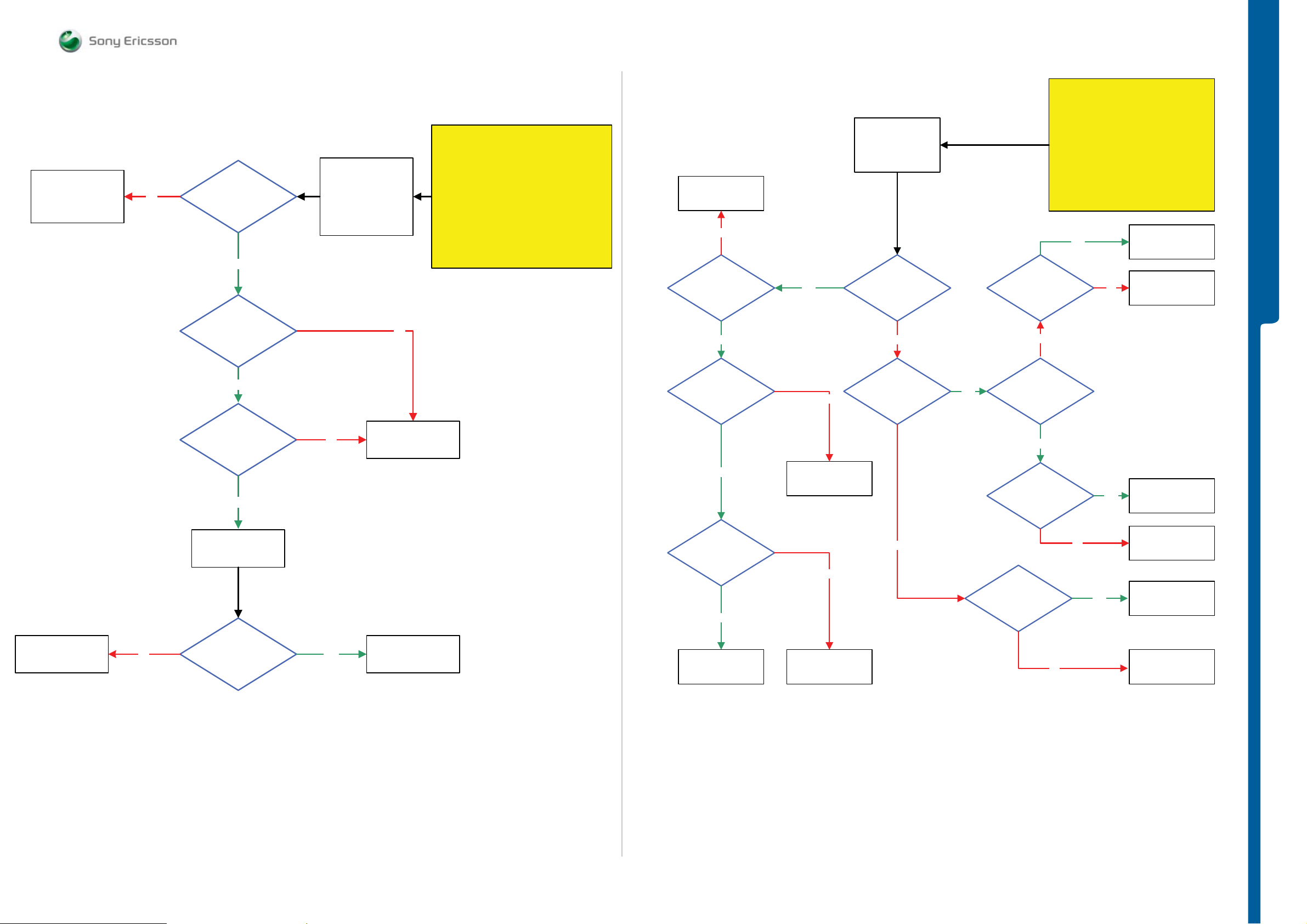
TROUBLESHOOTING Display Problems
/ Display Illumination Problems
SEMC Troubleshooting Manual
K850
Go to Display
illumination
problems
No
Display problems
Display Backlight
Ok
Yes
1.8 Volt DC
at
MP 5 (ST4200
VDDE18)
Yes
2.6 Volt DC
at
MP 4 (ST4201
VAUDIO26)
Yes
Use Fault Trace SW
MMI
Display pattern
Activate
Tri color pattern
No
SL 5 Replace
No
SL 4 Scrap
N2000
START
Step 1:
Use TRS Fixture and connect the display
and keypad. Connect VBATT.
If the display is working properly at the
TRS Fixture then replace the display
If not then continue with Step 2.
Step 2:
Load ITP SW into the phone
Use TRS Fixture and connect the display
Connect: VBATT and DCIO/SEPI
Continue with the
Display problems TRS guide
SL 5 Replace
N2000
SL 4 Scrap
No
1.8 Volt
Pulses at
MP 8 (R2206 OPTO_EN)
shortly after phone
Power On
Yes
3.0 Volt
Pulses at
MP 3 (TP2203 VOPTO30)
shortly after phone
Power On
Yes
Yes
No
Replace
N2201
Display illumination problems
Use Fault Trace SW
MMI
Misc
Activate
Display Backlight
Display Backlights
Ok
No
3.8 Volt DC at
MP 26 (TP4200)
Yes
at MP 49 (R4215) shortly
after Display Backlights
after Display Backlights
When Display Backlight
Use TRS Fixture and connect the display
and the keypad. Connect VBATT.
If the display is working properly at the
Use TRS Fixture and connect the display
Display illumination problems TRS guide
3.8V
Pk-Pk Pulses
is set
No
15V Pk-Pk
Pulses at
MP 26 (TP4200) shortly
Is set
Yes
0 Volt DC
At MP 25 (TP4201)
is activated
START
Step 1:
fixture then replace the display
If not then continue with Step 2.
Load ITP SW into the phone
Connect: VBATT and DCIO/SEPI
Yes
Step 2:
Continue with the
Replace
No
Yes
SL 5 Replace
SL 4 Scrap
Replace
X4200 or Display
V4200
N2000
TROUBLESHOOTING
SL 5 Replace
D2000
SL 4 Scrap
Replace
X4200
No Yes
Display
Ok
Claim Component
X4200
0.8 to 2.5
Volt Pulses at
MP 52 (N4200 Pin6)
shortly after phone
Power On
Yes
Flash the Phone with
EMMA
SUCR SW
No
Replace
N4200
No
3.8 Volt DC at
MP 51 (V4201
Anode)
No
No
Yes
SL 5 Replace
V4205 or N2000
SL 4 Scrap
Replace
V4201
SL 5 Replace
L4201
SL 4 Scrap
1203-2528 rev. 1
10 (101)
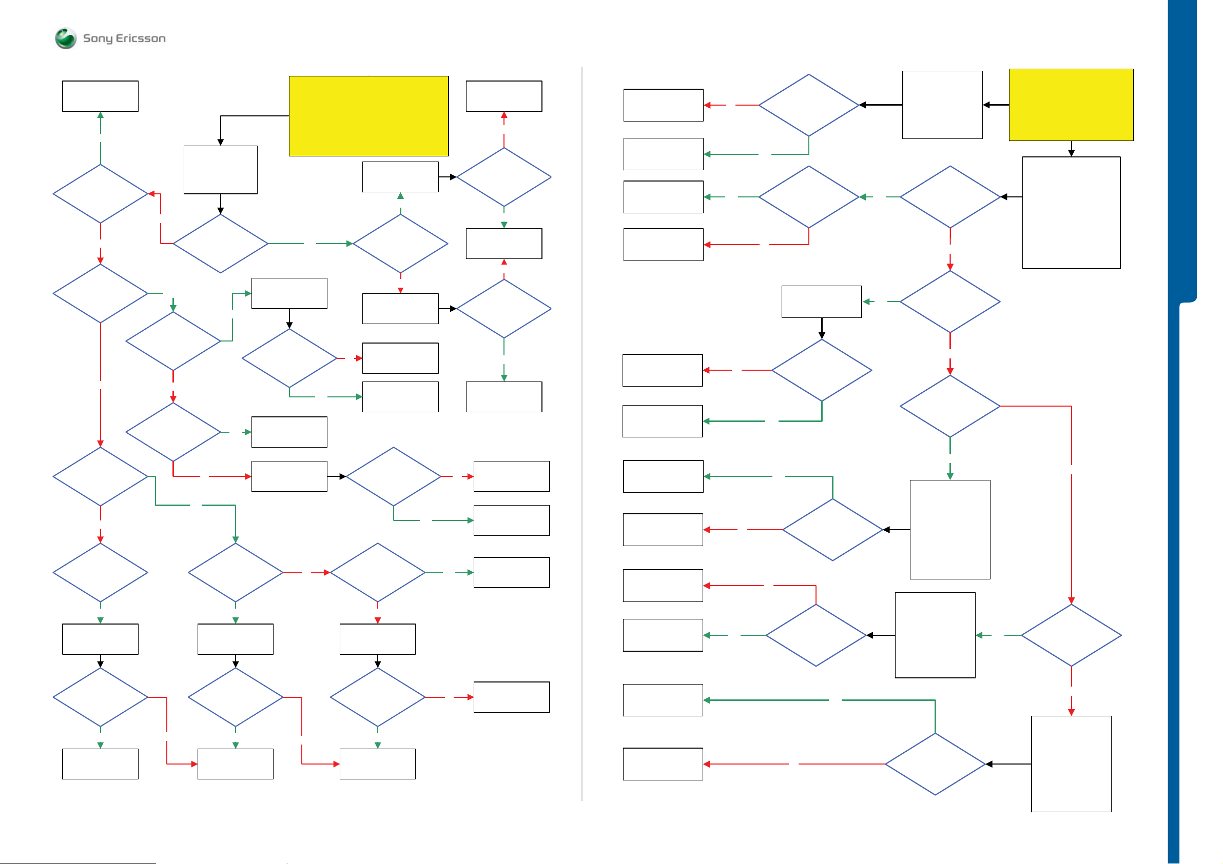
TROUBLESHOOTING Key Problems
/ LED Problems
SEMC Troubleshooting Manual
K850
Replace
V2402
Yes
Problem with
Phone Off
No
Problem with
Volume Down
key
No
Problem with
Volume Up
key
Perform Diode
Measurement
No
Problem with
Yes
More than
2.0 Volt DC between
MP 134 (S2402 A) and
MP 135 (S2402) C
No
Short circuit
between
MP 135 (S2402 C) and
MP PBA GND
No
Phone On
Yes
Volume Down key
MP 134 (S2402 A) and
Yes
Key problems
START
Use TRS Fixture and connect Display and
Perform Keyboard Test in Service Tests
If All Keys working properly at the
TRS Fixture then replace Keypad. If not then
disconnect VBATT and continue with the
Yes
Press the
S2402
0 Volt DC
between
MP 135 (S2402 C)
Yes
SL 5 Replace
V2478
SL 4 Scrap
Remove
S2402
Step 1:
Keypad. Connect: VBATT
Key problems TRS guide
Press the On/Off
MP PBA GND. More than
MP 127 (S2400 A)
No
2.0 Volt DC between
MP 134 (S2402 A) and
MP 135 (S2402 C)
key S2400
Yes
Connect the
black probe to
2.0 Volt DC at
No
Remove
S2400
Replace
S2402
SL 5 Replace
D2000
SL 4 Scrap
More than
MP 127 (S2400 A)
SL 5 Replace
2.0 Volt DC at
MP 127 (S2400 A)
No
Replace
S2400
No
0 Volt DC at
Yes
N2000
SL 4 Scrap
No
More than
Yes
Replace
S2400
SL 5 Replace
D2000
SL 4 Scrap
SL 5 Replace
N2000
SL 4 Scrap
Replace
V2428 Red LED
Replace
X2410
Replace
N4101
SL 5 Replace
N2000
SL 4 Scrap
Claim Component
X2410
Replace
N4101
No
Yes
No
MP 128 (C2427)
Yes
MP 18 (TP4112)
No
Yes
Yes
More than
1.8 Volt DC at
4.5 Volt DC
at
Replace
X2410
Keypad LEDs
Ok
LED problems
Yes
Yes
On Red LED
problems:
Use Fault Trace SW
MMI
LED and Backlight
Activate:
Red LED
Problem with all
Keypad LED
rows
No
Problem with any
of the Keypad LED
rows
No
Problem with
Camera Keypad
LED
Yes
Load ITP SW into the phone.
START
Use TRS Fixture
Connect: VBATT and DCIO/SEPI
Use Fault Trace SW
On Keypad LED
problems:
Connect Keypad
Use Fault trace SW
MMI
LED and Backlight
Activate:
Keypad Backlight
If Keypad LED works
properly at the
TRS Fixture then replace
Keypad
No
TROUBLESHOOTING
No
Problem
With all other
keys
Yes
Replace
X2410
Problem
solved
Yes
Claim
X2410
No
Yes
More than
2.0 Volt DC between
MP 132 (S2403 A) and
MP 131 (S2403 C)
Yes
Press the
Volume Up key
S2403
0 Volt DC
between
MP 132 (S2403 A) and
MP 131 (S2403 C)
Yes
SL 5 Replace
D2000
SL 4 Scrap
No
No
Short circuit
between
MP 131 (S2403 C) and
MP PBA GND
No
Remove
S2403
More than
2.0 Volt DC between
MP 132 (S2403 A) and
MP 131 (S2403 C)
Yes
Replace
S2403
Yes
Yes
No
Replace
S2402
SL 5 Replace
V2477
SL 4 Scrap
SL 5 Replace
D2000
SL 4 Scrap
Replace
X2410
Replace
X2511
Replace
N4101
SL 5 Replace
N2000
SL 4 Scrap
Replace
X2511
Yes
No
No
More than
0.8 Volt DC at
MP 162 (R4114)
MP 164 (R4115)
MP 163 (R4116)
1.8 Volt DC
at
MP 20 (TP4106
AF_LED)
Yes
No
Connect Keyflex to
the PBA
Use Fault trace SW
MMI
LED and Backlight
Activate:
Camera Keypad LED
Connect Single
Flash Assembly to
PBA
Use Fault trace SW
MMI
LED and Backlight
Activate:
Autofocus LED
More than
1.2 Volt DC
at MP 30 (R2544
LED_BACK)
Yes
Problem with
Autofocus LED
No
Camera Light Ring
problems:
Connect Single
Flash Assembly to
PBA
Use Fault trace SW
MMI
LED and Backlight
Activate:
Camera Light Ring
1203-2528 rev. 1
11 (101)
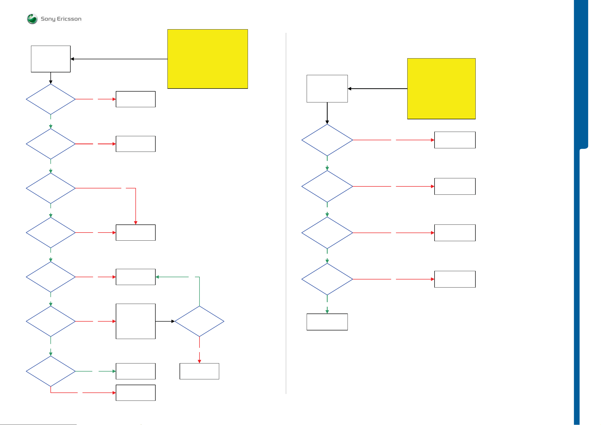
TROUBLESHOOTING Main Camera Problems
/ VGA Camera Problems
SEMC Troubleshooting Manual
K850
Fault Trace SW
MMI
Misc
Activate:
Main Camera Test
1.8 Volt DC at
MP 76 (R2280
CAM_LDO_EN)
Yes
2.8 Volt DC at
MP 32 (TP2204
VCAMAF)
Yes
Main Camera problems
No
No
Replace
D2420
Replace
N2206
START
Load ITP SW
into the phone.
Use TRS Fixture and
Connect: Display and Main Camera Module
Connect: VBATT and DCIO/SEPI
Use Fault Trace SW
If the Main camera module is not connected
or not working properly the Fault Trace SW
will show an error message in the Trace
window.
VGA Camera problems
Fault trace SW
MMI
Misc
Activate:
VGA Camera Test
1.8 Volt DC at
MP 76 (R2280
CAM_LDO_EN)
Yes
No
START
Load ITP SW
into the phone.
Use TRS Fixture and
connect Display and VGA Camera
Connect: VBATT and DCIO/SEPI
Use Fault Trace SW
If the VGA camera is not connected
or not working properly the Fault
Trace SW will show an error
message in the Trace window.
Replace
D2420
TROUBLESHOOTING
1.8 Volt DC at
MP 27 (TP2206
VCAMIO)
Yes
1.2 Volt DC at
MP 28 (TP2207
VCAML)
Yes
2.8 Volt DC at
MP 82 (ST2275
VCAMSA)
Yes
1.8 Volt DC at
MP 54 (TP2208
VCAMSD)
No
No
No
No
Replace
N2203
Replace
N2208
Fault Trace SW
Logic
GPIO Manager
Application
GPIO_11 Read
Yes
Is
Result GPIO_11
= High
1.8 Volt DC at
MP 27 (TP2206
VCAMIO)
Yes
2.8 Volt DC at
MP 82 (ST2275
VCAMSA)
Yes
13MHz at
MP 77 (R4301)
Yes
Replace
X4300
No
No
No
Replace
N2203
Replace
N2208
SL 5 Replace
D2000
SL 4 Scrap
Yes
26MHz at
MP 77 (R4301)
No
Yes
Replace
X4301
SL 5 Replace
D2000
SL 4 Scrap
No
Replace
D2420
1203-2528 rev. 1
12 (101)
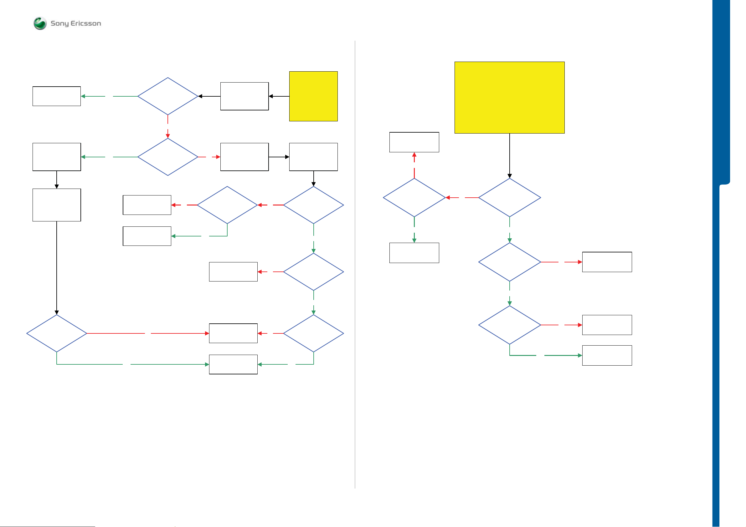
TROUBLESHOOTING Camera Door Problems
/ Vibrator Problems
SEMC Troubleshooting Manual
K850
Flash the Phone with
EMMA
SUCR SW
Disassemble the
phone
Use TRS Fixture
Fault trace SW
MMI
Misc
Activate:
Camera Door Test
Yes
Yes
Camera Door problems
Camera Door Test
Open/Close
Ok
No
Camera Door
Open position
Ok
Replace
D2420
No
Fault trace SW
MMI
Misc
Activate:
Camera Door Test
No
shortly after camera door
Disassemble the
Use TRS Fixture
1.8V,
225ms Pulses
test activation at
MP 91 (R2500)
phone
No
START
Load ITP SW
into the phone.
Insert the
Dummy Battery
Connect: VBATT and
DCIO/SEPI
Use Fault Trace SW
Fault trace SW
MMI
Misc
Activate:
Camera Door Test
3V, 225ms
Pulses shortly
after camera door test
activation at
MP 59 (TP2500)
SL 5 Replace
N2000
SL 4 Scrap
No
Is any of
C4206 or C4207
Short circuit
Vibrator problems
START
Load ITP SW into the phone
Use TRS Fixture.
Connect: VBATT and DCIO/SEPI
Use Fault Trace SW and go to:
If Vibrator is working properly at the
TRS Fixture then replace Vibrator if not
Continue with the Vibrator problems TRS guide
No
MMI-Misc
Activate:
Vibrator Test
2.8 Volt Pk-Pk
Pulses at
MP 141 (C4206
VIBR_OUT)
TROUBLESHOOTING
3V, 250ms
Pulses shortly
after camera door test
activation at MP 58
(TP2501)
Yes
Replace
N2500
No
Yes
Replace
V2500
Replace
D2420
Replace
X2511
No
No
Yes
3V,
225ms
Pulses shortly
after camera door test
activation at MP 93
(V2505 Pin 4)
Yes
3V, 225ms
Pulses shortly
after camera door test
activation at MP 55
(TP2502)
Yes
Yes
SL 5 Replace
C4206 or C4207
SL 4 Scrap
Yes
2.8 Volt Pk-Pk
Pulses at
MP 136 (X2506)
Yes
Connection
between
MP PBA GND and
MP 137 (X2507)
Ok
Yes
No
No
SL 5 Replace
L4202
SL 4 Scrap
SL 5 Replace
L4203
SL 4 Scrap
Clean Pad X2506
Clean Pad X2507
1203-2528 rev. 1
13 (101)
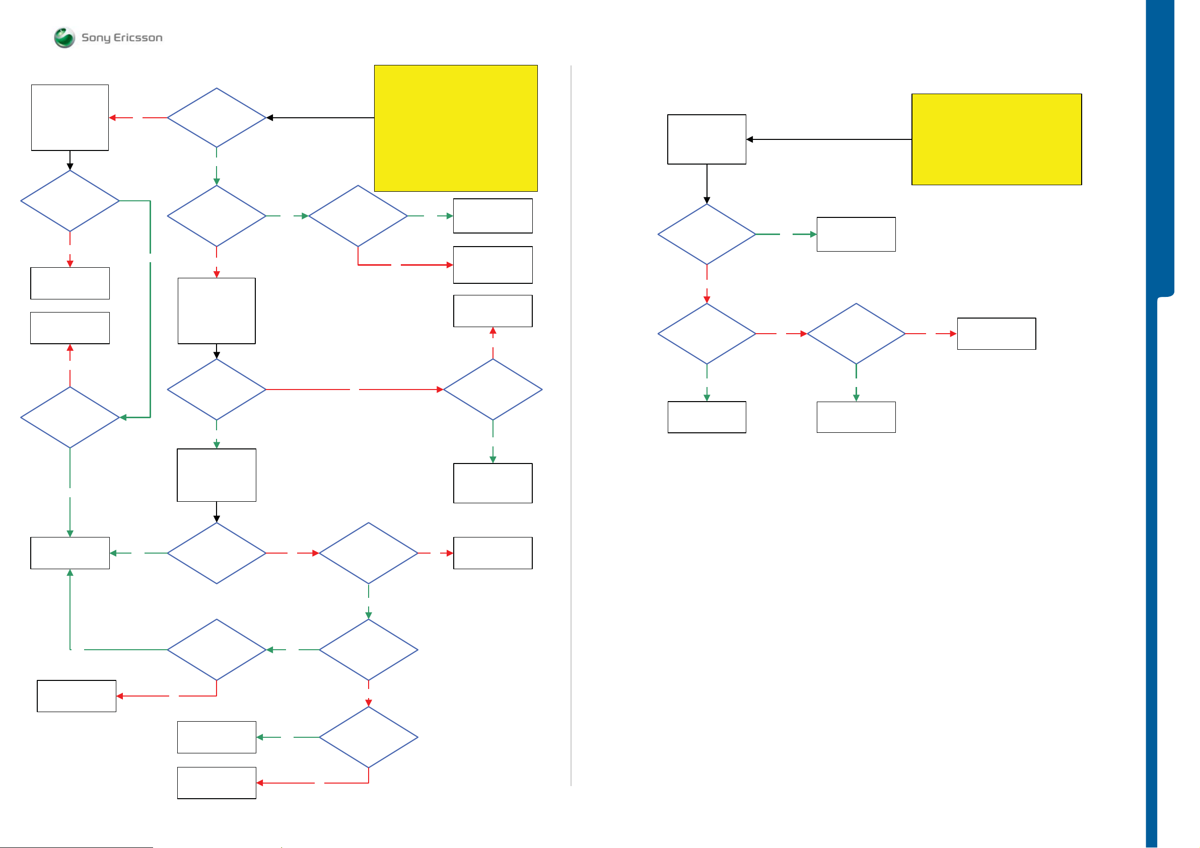
TROUBLESHOOTING Charging Problems
/ USB/ V BUS Cha rg in g Proble ms
SEMC Troubleshooting Manual
K850
Use TRS Fixture and
Fault Trace SW
Connect:
VBATT and
DCIO/SEPI
Start Battery
Calibration Test
3.2V
and 4.1V DC
at MP 31 (TP2200)
during Battery
Calibration
No
Replace
X2200
SL 5 Replace
R2200
SL 4 Scrap
No
Yes
Charging problems
Battery Calibration.
Passed
Yes
Current Calibration
Passed
No
Use TRS Fixture and
Fault Trace SW
Connect:
VBATT and
DCIO/SEPI
Yes
Is
MP 29 (TP2202)
Short circuit
To GND
Perform System Connector Protection Test
START
Load ITP SW into the phone
Connect: Dummy Battery
Connect:VBATT and DCIO/SEPI
Use Fault Trace SW:
Logic, Phone Power
Battery and Current Calibration
It is very important to follow
instrument settings instructions
when performing the Battery and Current
No
Perform
Calibration Test.
SL 5 Replace
Yes
Flash with EMMA
Charging Test
System Connector
N2000
SL 4 Scrap
SUCR SW
Go to
Replace
X2400
No
Connect
DSU-60/ USB cable
from PC to
the phone
5 Volt DC at
MP 44 (ST2201)
No
5 Volt DC at
MP 108 (R2470/1)
USB/VBUS Charging problems
SL 5 Replace
Yes
No
N2000
SL 4 Scrap
5 Volt DC at
MP 107 (R2470/2)
START
Perform System Connector Protection Test
If step 1 is Ok then continue with step 2.
Use Phone with Normal SW
No
Step 1:
Step 2:
Use TRS Fixture
Connect: VBATT
Replace
System Connector
X2400
TROUBLESHOOTING
No
Connection
between
PBA GND to Power
supply GND
Ok
Yes
SL 5 Replace
N2000
SL 4 Scrap
Yes
5 Volt DC at
MP 40 (C2201
DCIO)
Yes
Start
Current Calibration
(C.C.)
Phone
Consuming
more than 10mA
DCIO Current
(During C.C.)
R2201
0.1 Ohm
Phone
consuming more
No
MP 47
No
YesYes
(C2241 DCIO_INT)
Higher than
3,8 Volt DC
Yes
MP 41 (R2201)
CHSENSEP Higher
than 3,8 Volt DC
(During C.C.)
No
than 10mA
Charger (DCIO)
Current
Yes
SL 5 Replace
C2423 and C2424
SL 4 Replace
V2421
SL 5 Replace
N2000
SL 4 Scrap
Yes
Replace
N2402
Yes
SL 5 Replace
R2470
SL 4 Scrap
SL 5 Replace
R2201
SL 4 Scrap
No
Replace
V2202
SL 5 Replace
N2000
SL 4 Scrap
Yes
(V2202 Pin2)
CHREG Lower than
MP 47 (C2241)
(During C.C.)
No
No
MP 39
1203-2528 rev. 1
14 (101)
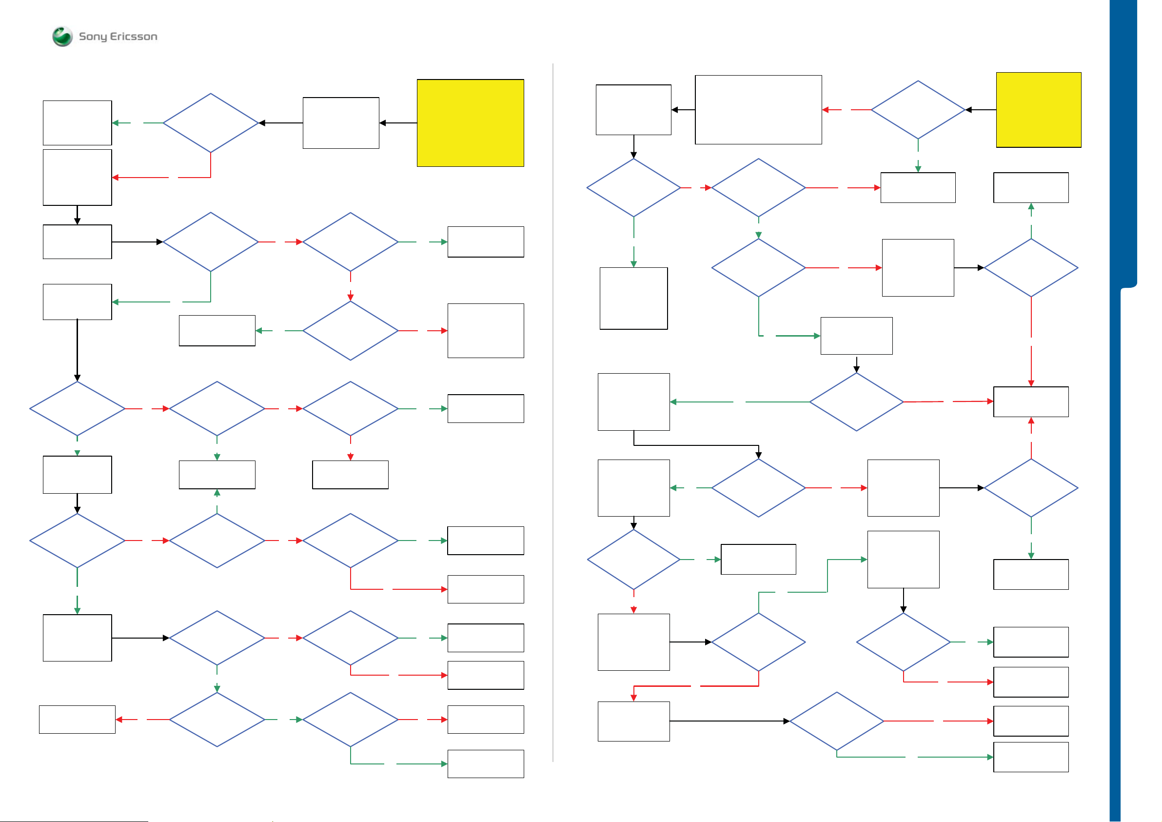
TROUBLESHOOTING SIM Problems
/ Memory Stick Problems
SEMC Troubleshooting Manual
K850
Replace combo
reader and
Flash the Phone
with EMMA
SUCR SW
Remove Test SIM
and Insert
Dummy SIM
Restart the Phone
Use:
Fault Trace SW
Activate:
SIMVCC
SIMVCC on
Activate:
SIMRST
Yes
Sim Com Test
Passed
No
1.8 Volt DC
At MP SIM1
(Fixture Sim reader
Pin 1)
Yes
SL 5 Replace
C2406 or C2411
SL 4 Scrap
SIM problems
No
Yes
Fault trace SW
Logic
SIM Card control
Activate:
SIM Com Test
1.8 Volt DC at
MP 50 (TP2400)
No
C2406
or C2411
Short circuit
Load ITP SW into the phone.
START
Use TRS Fixture.
Connect: Fixture Combo
reader to the PBA and
Insert Test SIM
Connect:
VBATT and DCIO/SEPI
Use Fault Trace SW
Yes
No
Replace
X2409
SL 4 Replace
X2409
If still faulty
SL 5 Replace
N2000
SL 4 Scrap
Fault trace SW
Logic
SIM Card control
Activate:
Memory Stick Test
Memory Stick Test
Passed
Yes
Replace Combo
Reader and
Flash the Phone
with
EMMA
SUCR SW
Memory Stick problems
Load ITP SW
into the phone.
Use TRS Fixture
Fixture Combo reader to PBA
Connect : VBATT and DCIO/SEPI
No
Connect:
Insert Memory Card
Use Fault Trace SW
0 Volt DC at
MP 105 (R2406
MSDETECT)
Yes
1.8 Volt DC at
MP 94 (R24102
CMDDIR
D2410 Pin 4)
Yes
No
No
No
Restart the phone
and measure the
pulses after 5 sec
Is
X2409
damaged
Yes
Replace
X2409
Disconnect Combo
reader and restart
the phone, measure
the pulses after
5 sec
START
SL 5 Replace
D2410
SL 4 Scrap
Yes
1.8 Volt at
MP 95 (R24102
MCCMDDIR
D2410 Pin 3)
No
TROUBLESHOOTING
1.8 Volt DC at
MP SIM2 (Fixture SIM
reader Pin 2)
Yes
SIMVCC on
SIMRST on
Activate:
SIMCLK
1.0 Volt DC at
MP SIM3 (Fixture Sim
reader Pin 3)
Yes
SIMVCC on
SIMRST on
SIMCLK on
Activate:
SIM DATA
No
No
1.8 Volt DC at
MP 69 (TP2401)
Yes
Replace
X2409
Yes
1.0 Volt DC at
MP 65 (TP2402)
1.8 Volt DC at
MP SIM7 (Fixture SIM
reader Pin 7)
Yes
No
No
No
C2410
Short circuit
No
SL 5 Replace
N2000
SL 4 Scrap
C2408
Short circuit
1.8 Volt DC at
MP 70 (TP2403)
No
No
Yes
Yes
Yes
SL 5 Replace
C2410
SL 4 Scrap
Sl 5 Replace
C2408
SL 4 Scrap
SL 5 Replace
N2000
SL 4 Scrap
Replace
X2409
SL 5 Replace
N2000
SL 4 Scrap
Disconnect Combo
reader and restart
the phone, measure
the pulses after
5 sec
Restart the phone
after each
measurement.
Measure pulses
after 5 sec.
1.8 V to 2.8V
at MP 63 (R24106)
to MP 64 (R24110)
No
Restart the phone
Measure pulses
after 5 sec.
Yes
No
Yes
Yes
2.8 Volt at
MP 66 (R24105
MC_CLK)
Replace
X2409
Yes
1.8 V to 2.8V
at MP 103 (R2490)
1.8 Volt at
MP 96 (SP2408
MCDATDIR)
repair instructions
No
At MP 98 (R2444) to
Cut the fence
according to the
for D2460. Restart
the phone and
measure pulses
after 5 sec.
Restart the phone
after each
measurement.
Measure pulses
after 5 sec.
From High to
Low pulses Signal
MP 99 (R2448)
No
No
Yes
SL 5 Replace
D2000
SL 4 Scrap
No
1.8 Volt at
MP 100 (R2496
MCCLK)
Yes
Replace
D2460
Replace
D2460
SL 5 Replace
D2000
SL 4 Scrap
Replace
X2409
No
Connection
Between MP PBA GND
and MP SIM5 (Fixture
Sim reader Pin 5)
Ok
Yes
10 Kohm
Between MP 50
(TP2400) and MP 70
(TP2403)
Yes
No
SL 5 Replace
R2419
SL 4 Scrap
SL 5 Replace
N2000
SL 4 Scrap
Restart the phone .
Measure pulses
after 5 sec.
1.8 V to 2.8V
at MP 104 (R24101)
Yes
No
SL 5 Replace
N2000
SL 4 Scrap
Replace
D2460
1203-2528 rev. 1
15 (101)
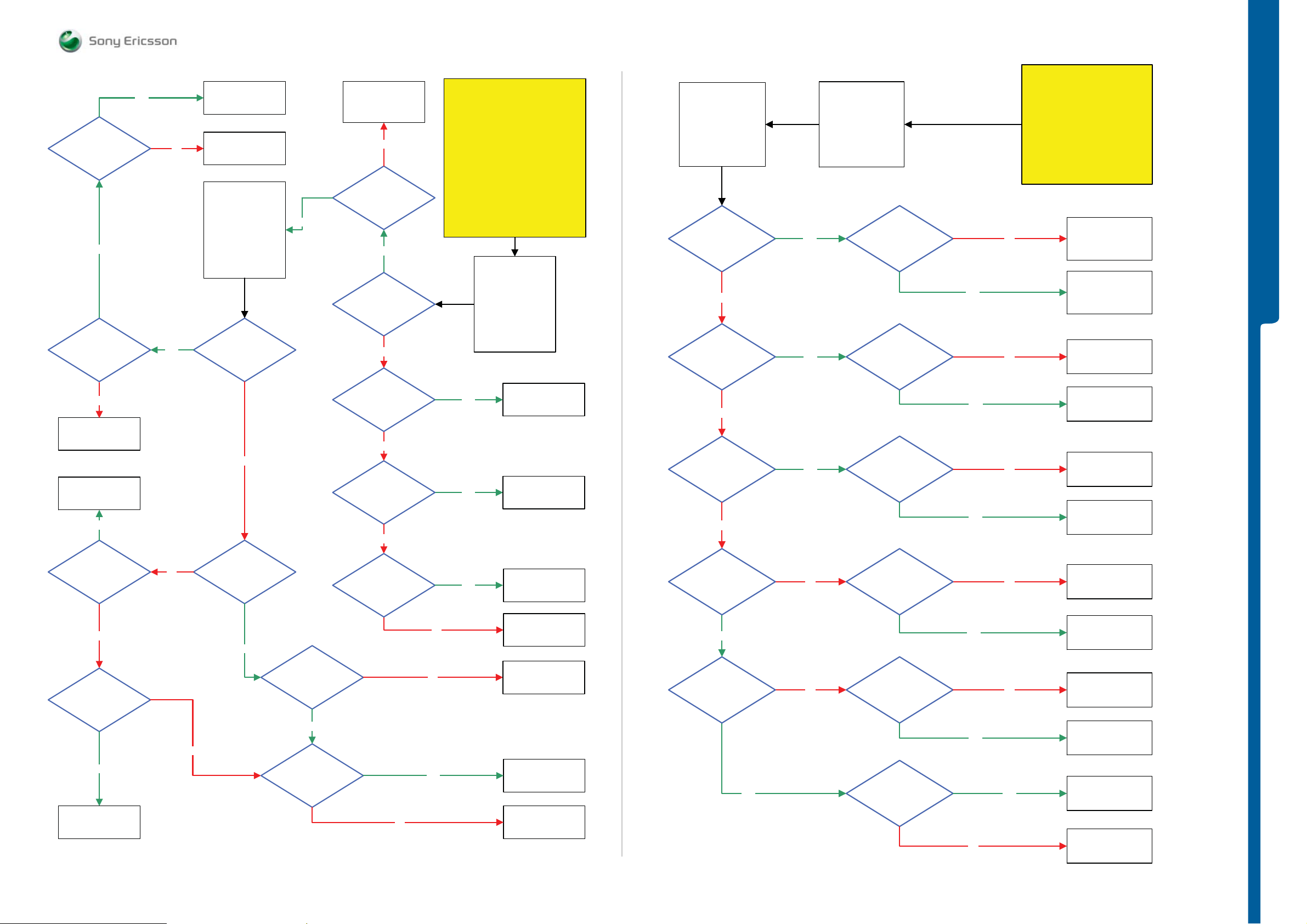
TROUBLESHOOTING Audio Internal Problems
/ Audio Exter n al Problem s
SEMC Troubleshooting Manual
K850
0 Volt DC
at MP 160
(V2405_ Pin 6)
Yes
2.6 Volt DC
at MP 124 (ST2441)
No
Replace
N2400
SL 5 Replace
L3108 and L3109
SL 4 Scrap
Yes
Yes
Yes
No
Audio Internal problems
Go to
Audio External
Problems
Replace
V2405
Fault Trace SW
Audio and FM Radio
Audio Loop test
Audio Input: Mic1
Loop Mode: Analog
Audio Output:
Loudspeaker
Apply Audio Loop
Whistle into the
PBA Mic
More than
100mV AC Pk-Pk
at MP 74 (X3102) and
MP 75 (X3103)
No
Yes
SL 5 Replace
L3103,L3104,
L3110,L3111
SL 4 Scrap
No
More than
100mV AC Pk-Pk
at MP 1 (X3100) and
MP 2 (X3101)
Yes
More than
100mV AC Pk-Pk
at MP 43 (L3103 BEARP)
and MP 45 (L3104
BEARN)
No
More than
100mV AC Pk-Pk at
MP 37 (ST3100)
No
2.2 Volt DC
at MP 106 (R3109
CCO_INTMIC)
No
START
System Connector Protection Test
Use TRS Fixture. Connect Display
perform Audio Service Tests. If all
Audio Service Tests work properly at
the fixture then replace Loudspeaker
and continue with the Audio internal
Step 1: Perform
Step 2:
and Keypad. Connect VBATT and
or Earphone
Load ITP SW into the phone.
Connect VBATT and DCIO/SEPI
Yes
Yes
If not then
Use TRS Fixture.
Use Fault Trace SW
problems TRS guide
Fault Trace SW
Audio and FM Radio
Audio Loop test
Audio Input: Mic1
Loop Mode: Analog
Audio Output:
Earphone
Apply Audio Loop
Whistle into the
PBA Mic
SL 5 Replace
N2000
SL 4 Scrap
Replace
Electret Mic or
X3105
Disconnect
DCIO/ SEPI cabel
and Insert PHF set
Whistle into the AUX
mic
Can you
hear at AUX
earphone when you
whistle in to the
AUX mic
No
More than
80mV AC Pk-Pk
at MP 112 (L2403 SPL) and
MP 113 (L2404 SPR) When
whistle in to the
AUX mic
No
More than
20mV AC Pk-Pk at
MP 109 (R3130 MICP_int)
and MP 89 (R3131
MICN_int)
No
Audio External problems
Fault trace SW
Audio and FM Radio
Audio Loop test
Audio Input: AUX1
Loop Mode: Analog
Audio Output:
AUX Earphone
Apply Audio Loop
Yes
Yes
Yes
Audio Internal
Tested
L2403 and L2404
Ok
More than
20mV AC Pk-Pk at
MP 88 (C3155) and
MP 87 (C3156)
Yes
Yes
Yes
START
Step 1: Perform
System Connector Protection
Connect: VBATT and DCIO/SEPI
No
No
No
Test
Step 2:
Load ITP SW into
the phone.
Use TRS Fixture
Use Fault Trace SW
Audio Internal
problems
Flash the Phone
with EMMA
SUCR SW
SL 5 Replace
L2403 or L2404
SL 4 Scrap
Replace
System Connector
X2400
SL 5 Replace
N2000
SL 4 Scrap
Replace
N3101
TROUBLESHOOTING
Go to
1.9 Volt DC
at MP 139 (V3101_Pin 1)
and MP 138 (V3101_Pin
2)
No
Is any of
C3137 and C3160
Short circuit
Yes
Replace
Faulty Component
No
1.9 Volt DC
at MP 74 (X3102) and
MP 75 (X3103)
No
Yes
More than
100mV AC Pk-Pk
at MP 38 (C3137) and
MP 42 (C3160)
Yes
1.8 Volt DC
at MP 19 (TP3100
AMPCTRL)
2.2 Volt DC
at MP 35 (L3105
CCO1)
No
No
Yes
No
Yes
SL 5 Replace
N2000
SL 4 Scrap
SL 5 Replace
L3105
SL 4 Scrap
SL 5 Replace
N2000
SL 4 Scrap
Replace
N3100
Replace
D2420
Connection
between
MP 114 (X2400_Pin 3)
and MP 110 (L2401)
Ok
Yes
Connection
between
MP 115 (X2400_Pin 4)
and MP 111 (L2402)
Ok
Yes
No
L2401
Ok
No
Yes
No No
L2402
Ok
Yes
2.2 Volt DC at
MP 86 (R3156)
Yes
No
SL 5 Replace
L2401
SL 4 Scrap
Replace
System Connector
X2400
SL 5 Replace
L2402
SL 4 Scrap
Replace
System Connector
X2400
Replace
N3101
SL 5 Replace
L3106 or N2000
SL 4 Scrap
1203-2528 rev. 1
16 (101)
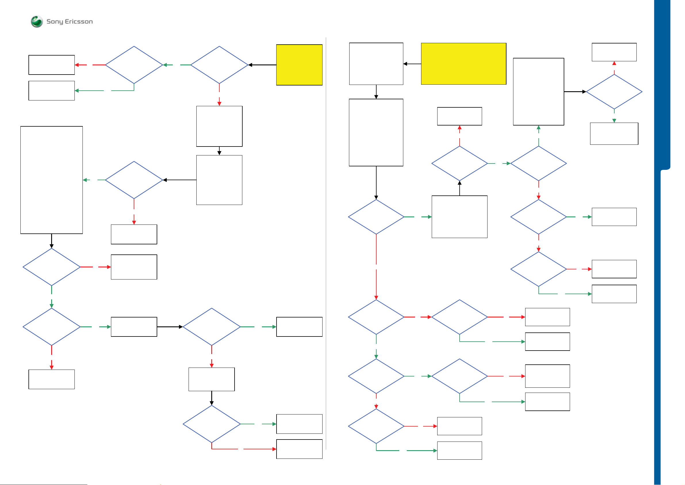
TROUBLESHOOTING FM Radio Problems
/ Bluetooth Problems
SEMC Troubleshooting Manual
K850
Replace
N3101
SL 5 Replace
N2000
SL 4 Scrap
Disconnect:
DCIO/SEPI Cable
Connect:
Customized FM Radio Cable
Black Lab Plug to
TRS Fixture GND Input and
PHF Connector to the Phone
System Connector
Signal Generator
Instrument Settings:
Frequency:
Use free Freq. Channel
Example:
103 MHz in Sweden
Amplitude: 25.0 uVrms
FM Dev: +/-22.5 kHz
FM Rate: 1kHz
FM Radio problems
PHF
No Yes
Yes
working properly
during
Voice call
Yes
3.8 Volt DC
at MP 151 (ST2282)
and 1.8V at
MP 154 C3305
No
SL 5 Replace
N2000
SL 4 Scrap
Speaker and
FM Radio Tests
working properly
No
Load ITP SW
into the phone.
Use TRS Fixture
Connect VBATT and
DCIO/SEPI
Use Fault Trace SW
Fault trace SW
Audio and FM Radio
FM Radio
Audio Output
Loudspeaker
Frequency
According to
Instrument Settings
Set FM Radio
START
Go to
Service Tests and
Perform:
Speaker and
FM Radio Test
Load ITP SW
Into the phone
Use TRS Fixture
Connect:
VBATT and DCIO/SEPI
Use Fault Trace SW
Fault trace SW
TX and RX
Bluetooth
Channel 0
Set MaxPwr MOD 0
Use
Spectrum Analyzer
Instrument settings:
Frequency: 2402 MHz
Span: 1MHz
Amplitude: -5dBm
Use Peak Search
Signal
At MP 142 (X1400
BT_ANT)
Bluetooth problems
START
Flash the phone with the
EMMA SUCR SW and retest the phone.
If successful claim SW Flashing
If not then continue with
Bluetooth problems TRS guide.
Replace
N1400
No
Is
MOD 1 Freq.
Minimum 230 KHz
higher then
MOD 0 Freq.
Fault Trace SW
TX and RX
Bluetooth
Yes
Channel 0
Set MaxPwr MOD 1
Use Spectrum Analyzer
with the previous
instrument settings
Yes
Change the
Bluetooth channels
In Fault Trace SW
and test the output.
Use
Spectrum Analyzer
Span 10MHz
Use Peak Search when
changing the channel.
Note:
1MHz channel spacing
Yes
-20dBm at
MP 142 (X1400
BT_ANT)
(±5dBm)
No
-15dBm at
MP 78 (Z1400 Pin 1)
(±5dBm)
No
Yes
Replace
N1400
No
All channel
passed
TROUBLESHOOTING
Yes
Replace
BT Antenna
and clean
X1400 and X1401
SL 5 Replace
C1402 and L1402
SL 4 Scrap
Any signal at
MP 156 (C3145)
MP 155 (C3146)
Yes
Can you
hear 1KHz ton at
TRS Fixture
Loudspeaker
No
SL 5 Replace
N2000
SL 4 Scrap
No
Yes
SL 4 Replace
N1400
SL 5 Replace
L3300 and C3306
Replace
System Connector
X2400
Signal
Ok
No
SL 4 Replace
V2425
SL 5 Replace
L2405 and C2434
Signal
Ok
Yes
Yes
Claim
System Connector
X2400
Claim
Component
No
26 MHz Signal
At MP 148 (R2118
BT_CLK)
Yes
2.7 Volt DC at
MP 14 (ST2212
VBT27)
No
C2205
Short circuit
No
Yes
No
More than
60KOhm
between MP 148
(R2118) and
PBA GND
1.8 Volt DC at
MP 9 (ST2208 VDDE18)
and 2.7 Volt DC at MP 34
(ST2213 VDIG)
SL 5 Replace
N2000
SL 4 Scrap
Yes
Yes
MP 144 (Z1400_Pin 5)
MP 145 (Z1400_Pin 7)
No
No
-15dBm at
and
(±5dBm)
Yes
Replace
N1400
SL 5 Replace
D2105
SL 4 Scrap
SL 5 Check C2214
and C2215 then
Replace N2000
SL 4 Scrap
Replace
N1400
No
Replace
N1400
SL 5 Replace
Z1400
SL 4 Scrap
No
Replace
N1400
Yes
SL 5 Replace
C2205
SL 4 Scrap
1203-2528 rev. 1
17 (101)
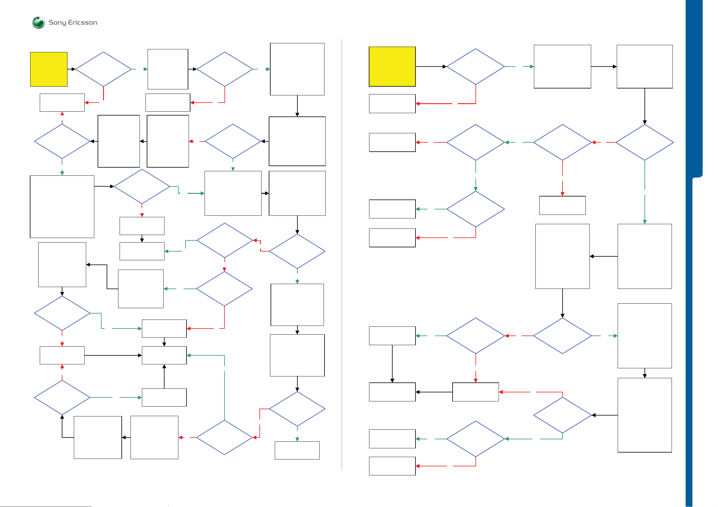
TROUBLESHOOTING GSM Network Problems
/ WCDMA Networ k Problem s
SEMC Troubleshooting Manual
K850
START
Replace
X1200
No
Is
Max Pwr 23dBm
Ok
(±3dBm)
Yes
Perform RSSI Test at
GSM 900, 1800 and 1900 Band
Instrumet Settings
System Mode:
TX/RX Tester Mode (GSM)
GSM BAND:
E-GSM 900, Channel 124
E-GSM 900, Channel 975
DCS 1800, Channel 512
PCS 1900, Channel 512
Measurement Mode:
RF Power -60dBm, Repeat, CW
Use
Spectrum Analyzer
Instrument settings:
TX Freq: 824.2MHz
Span: 300KHz,
Amplitude: -5dBm
Measure with
RF Probe
Signal at
MP 130 (Z1001)
-12dBm (±
(Inside GSM module)
MP 129 (L1006)
5dBm)
No
Replace
N1002
No
Signal at
-20dBm
(±15dBm)
MP 73 (R1201) and
Spectrum Analyzer
Instrument settings:
TX Freq: 1710.2MHz
Span: 300KHZ,
Amplitude: -5dBm
Measure with
RF Probe
0 Ohm
Between
MP 72 (L1200)
Instrument
Settings:
System Mode:
TX/RX Tester Mode
(WCDMA)
Downlink Channel:
10562
Measurement
Mode:
Repeat, Burst
Yes
Yes
Use
GSM Network problems
Load the ITP SW
into the phone.
Use TRS Fixture
Connect VBATT
Yes
and DCIO/SEPI
Fault Trace SW
Fault Trace SW
TX and RX WCDMA
Radio Settings:
Modes: Max Pwr
All Bands
Passed
RSSI Test
No
Replace
N1200 Thor
Go to
SERP Calibration
Fault Trace SW
Switch GSM Mode
Settings to:
TX Static
N1200 Thor
SERP Calibration
N1200 Thor
Fault Trace SW
Switch GSM Mode
Settings to:
TX Static
Use
SL 5 Replace
N2000
SL 4 Scrap
Select Band:
BAND I
Fast Select
Channels:
Ch LOW
23dBm
Replace
Go to
Replace
Yes
Yes
Yes
No
2.8 Volt DC at
MP 12 (ST2215
VccA)
NoNo
No
RSSI Test
Passed
Instrument Settings:
System Mode:
TX/RX Tester Mode (GSM)
GSM BAND: GSM850
Measurment Mode:
Repeat, Burst
Correction: 1.6dB
Is
measured value
±
5dBm
No
1.4V-1.6V Pk-Pk
Pulses at
MP 133 (R1000
VAPC)
No
Yes
Is
measured value
±
5dBm
Yes
Connect Mobile Phone
Instrument Settings:
System Mode:
TX/RX Tester Mode (GSM)
Yes
No
No
GSM BAND: GSM850
RF Power ON: -60dBm
Measurement Mode:
Repeat, CW
Correction: 1.6dB
Fault Trace SW
TX and RX GSM
GSM Mode Settings:
RX Switched
GSM Radio Settings:
Select Band: GSM 850
Channel: 128
GSM RSSI Measurements:
Start RSSI Test
Fault Trace SW
TX and RX GSM
GSM Mode Settings:
TX Switched
GSM Radio Settings:
Select Band : GSM 850
Channel : 128
Power Level: 5
measured value
33dBm
(±3dBm)
Instrument Settings:
System Mode:
TX/RX Tester Mode
GSM BAND: DCS1800
Measurement Mode:
Repeat, Burst
Fault Trace SW
TX and RX GSM
GSM Mode Settings:
TX Switched
GSM Radio Settings:
Select Band : GSM 1800
Channel : 512
Power Level: 0
measured value
30dBm
(±3dBm)
WCDMA Network
problems
Tester
Is
Yes
(GSM)
Is
Yes
Go to
START
Before TRS WCDMA
the GSM TRS guide
must be done!
Replace
X1200
SL 5 Replace
D2000
SL 4 Scrap
Replace
N2205
SL 5 Replace
N2000
SL 4 Scrap
Replace
N1200
Go to
SERP
Calibration
Replace
Faulty Component
Go to
GO-NOGO
Test
No
Yes
Yes
Yes
0 Ohm
between
MP 73 (R1201) and
MP 72 (L1200)
No
1.8Volt DC at
MP 81 (R2220
DCDC_EN)
1.3V-1.8V DC at
MP 83 (R2221
WPAVCC)
No
Current
consumption
between
500 – 800 mA
Replace
N1210
Are any of
X1201,
X1202 or X1203
damaged
No
WCDMA Network problems
Yes
DCIO/SEPI: 5V, Limiter 2A
Yes
Yes
No
No
No
Yes
Load ITP SW
into the phone.
Use TRS Fixture
Connect:
VBATT: 3.8V, Limiter 3A
Use Fault Trace SW
3.4V-3.8V DC at
MP 80 (L2210
VBATI)
No
SL 5 Replace
L2210
SL 4 Scrap
Instrument Settings:
System Mode:
TX/RX Tester Mode
WCDMA
Downlink Channel:
BAND I: 10562
BAND II: 9662
BAND V: 4375
Measurement Mode:
Repeat
Correction: 1.6dB
Max Pwr.
23dBm (±3dBm)
all bands
Ok
Phone reports
correct values
At all bands
(±3dBm)
Fault Trace SW
TX and RX WCDMA
Radio Settings:
Fast Select Channels:
Modes: Max Pwr 23dBm
3.4V-3.8V DC at
No
Fault Trace SW
TX and RX WCDMA
Radio Settings:
BAND I, II and V
Fast Select Channels:
Modes: Max Pwr 23dBm
Test Max Pwr 23dBm
for each WCDMA Band
Only one WCDMA Band
Instrument Settings:
System Mode:
TX/RX Tester Mode
Downlink Channel:
Yes
BAND I: 10562
BAND V: 4375
Measurement Mode:
RF Power: ON (-60dBm)
Correction: 1.6dB
Fault Trace SW
TX and RX WCDMA
Radio Settings:
Fast select channels:
Modes: Read RSSI
Read Measurement
Test Read RSSI
for each WCDMA Band
Only one WCDMA Band
Select Band:
BAND I
Ch LOW
TROUBLESHOOTING
MP 84 (L2207
VCC_WPA)
Yes
Select Band:
Ch LOW
at the time
WCDMA
BAND II: 9662
Repeat
Select Band :
BAND I, II, V
Ch LOW
RX On:
at the time
1203-2528 rev. 1
18 (101)
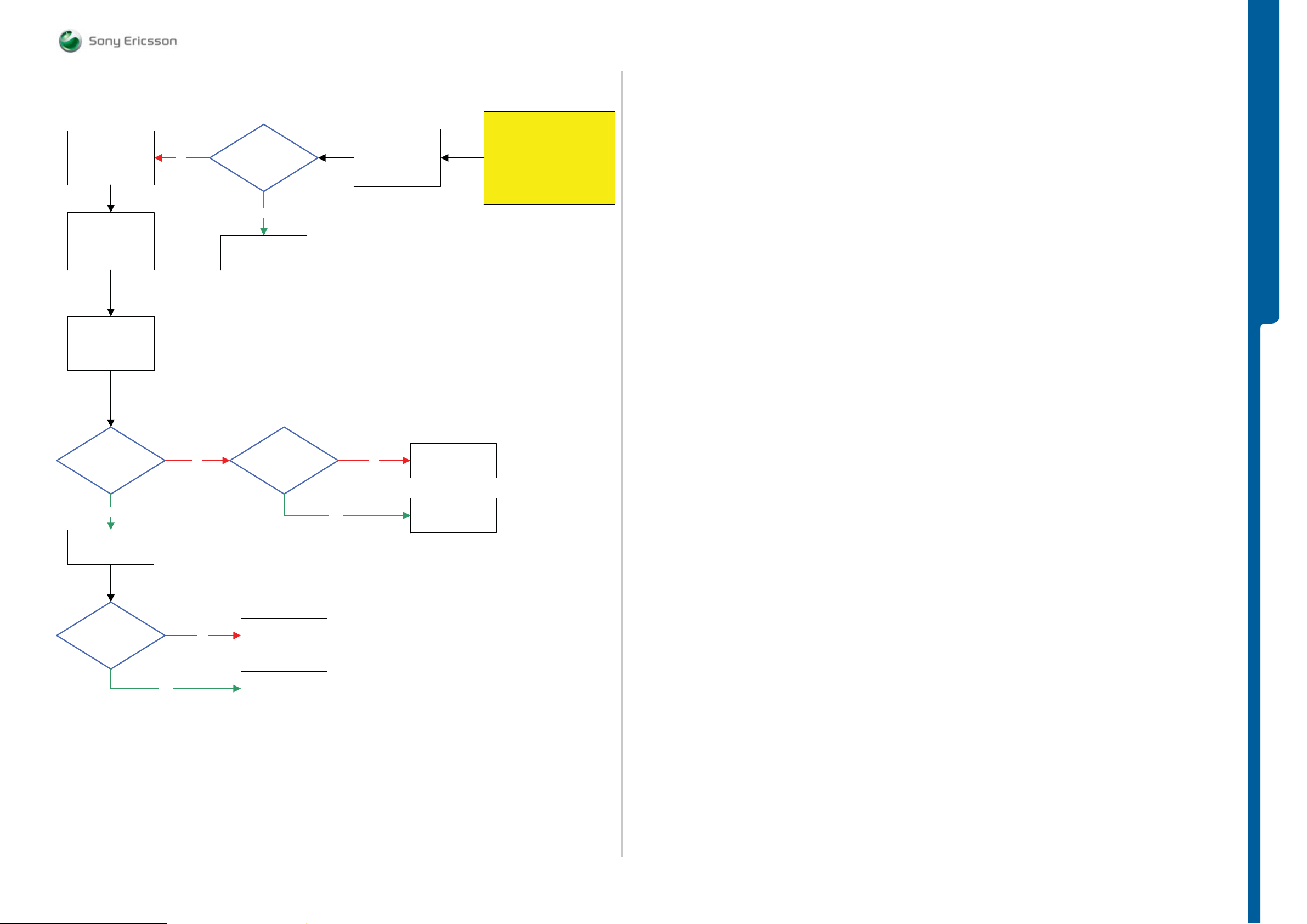
Xenon Flash problems
TROUBLESHOOTING Xenon Flash Problems
SEMC Troubleshooting Manual
K850
Disassemble the
phone
Use TRS Fixture
Connect Display and
Main Camera
Fault trace SW
MMI
Led and Backlight
Activate:
Xenon Flash Test
Disconnect
Main Camera
1.8 Volt DC
At
MP 92 (R4305)
No
Xenon Flash Test
Flash the Phone with
No
Ok
Yes
EMMA
SUCR SW
1.8 Volt DC
MP 90 (R4304)
Fault trace SW
MMI
Led and Backlight
Activate:
Xenon Flash Test
Connect: VBATT and DCIO/SEPI
START
Load ITP SW
into the phone.
Insert Dummy Battery
Use Fault Trace SW
TROUBLESHOOTING
At
No
Replace
D2420
Yes
Replace
X2511
Problem
solved
Yes
No
SL 5 Replace
D2000
SL 4 Scrap
Claim Component
X2511
Yes
SL 5 Replace
D4300
SL 4 Scrap
1203-2528 rev. 1
19 (101)
TROUBLESHOOTING System Connector Protection Test
/ Current Comsu m pt ion Test
SEMC Troubleshooting Manual
K850
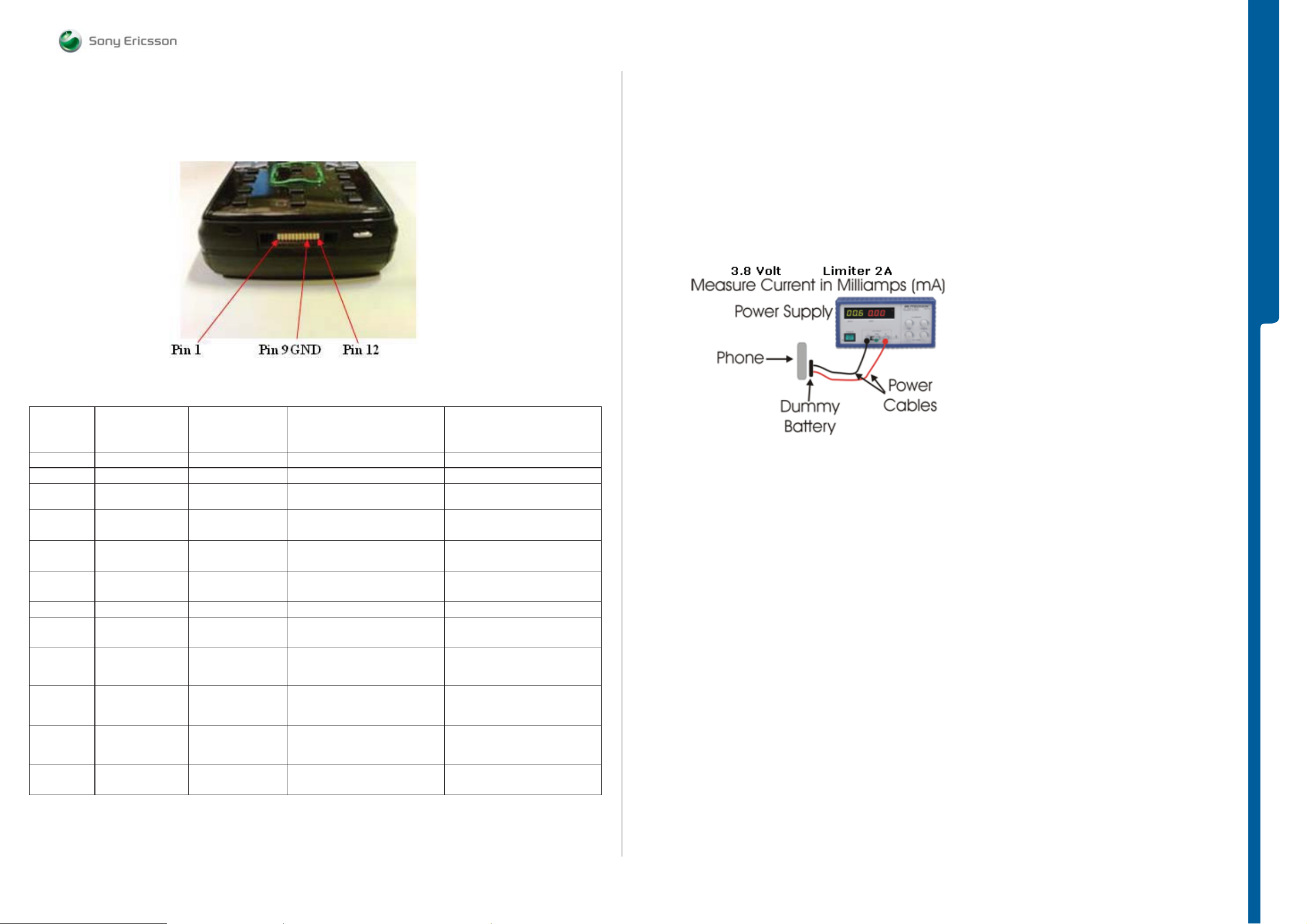
System Connector Protection Test
Perform Diode and Ohm measurements with DMM
Connect the black probe at ground (Pin 9 system connector)
Current Consumption Test
Step 1:
Insert Local SIM Card and use the phone with the Normal SW (SSW) and dummy
battery connected to Power Supply Channel 1 VBATT according to Picture 1.
Instrument settings: Voltage: 3.8 Volt, Limiter 3A.
TROUBLESHOOTING
Measure the current when Phone is off. Check the current consumption at Power
Supply Channel 1 VBATT.
Picture 1
Diode
Pin at
X2400
1 0L 0L N2402 if Not 0L C2422 if Not 0L
2 0.0 1.4 No Action L2405 If higher than 1.4Ω
3 2.0 12K
4 1.0 1K
5 2.0 9K
6 2.0 9K
7 0L 0L Not connected Not connected
8 1.4 1.5K V2420 if lower than 1.5KΩ
9 0 0 No Action
10 0.7 200K-470K N2401if lower than 200KΩ
11 1.0 200K-470K N2401if lower than 200KΩ
12 0L 80K V2421 if lower than 80KΩ
Measurement
/ Volt
Ohm
Measurement
/ Ohm
SL 4 Action SL 5 Action
N3101 if lower than 12KΩ
L2401 if higher than 12KΩ C2421 If lower than 12KΩ
N3101 if lower than 1KΩ
L2402 if higher than 1KΩ C2420 if lower than 1KΩ
N3101 if lower than 9KΩ
L2403 if higher than 9KΩ C2416 if lower than 9KΩ
N3101 if lower than 9KΩ
L2404 if higher than 9KΩ C2415 if lower than 9KΩ
R2451, R2440, R2436
if higher than 1.5KΩ
R2455 if Not 0Ω between
X2400_Pin9 and PBA GND
D2450 if lower than
200KΩ R2465 if higher
than 470KΩ
D2450 if lower than
200KΩ R2466 if higher
than 470KΩ
C2423, C2424
if lower than 80KΩ
Current consumption in off mode should be less than 1mA.
If more than 1mA go to Dead Phone problems part 1 TRS guide.
Step 2:
Start the phone:
Measure the deep sleep current max 6mA typical between 0-3mA.
Make sure that the operator is running with deep sleep. (This operation can be
switched off by operator if the network is busy).
If phone using more than 6mA, then go to EMMA III and perform Software Update
Contents Refresh (SUCR).
Step 3 with Mobile Phone Tester Instrument
Insert Test SIM Card and use the phone with the Normal SW (SSW) and dummy
battery connected to Power Supply Channel 1 VBATT according to Picture 1.
Instrument settings: Voltage: 3.8 Volt, Limiter 3A.
Use Mobile Phone Tester Instrument in signalling mode direct connected to the
phone with RF Connector or use Shield Box if not possible. Phone Display must be
on during these tests to get correct current measurements.
Perform Radio TX measurements at GSM and WCDMA Band and compare with limits
according to text below.
1203-2528 rev. 1
20 (101)

TROUBLESHOOTING Current Comsumption Test
SEMC Troubleshooting Manual
K850
- Transmitter current 850 MHz at Ch: 128 power level 5. Typical 400mA
- Transmitter current 900 MHz at Ch: 1 power level 5. Typical 400mA
- Transmitter current 1800 MHz at Ch: 512 power level 0. Typical 400mA
- Transmitter current 1900 MHz at Ch: 512 power level 0. Typical 400mA
- Transmitter current WCDMA BAND I Low RX Ch: 10562 at 23dBm output
power. Max 750mA
If current consumption is not correct, the fault could be fixed by running SERP
calibration if not then go to GSM and WCDMA Network problems TRS guides.
If the current consumptions are equal to test limits then go to Charging Test.
Step 4 with Fault Trace SW application:
- Flash the phone with ITP SW
-Use TRS Fixture
- Connect the:
Power Supply Channel 1 VBATT:
Instrument settings: Voltage: 3.8 Volt, Limiter 3A
Power Supply Channel 2 DCIO/SEPI
Instrument settings: Voltage: 5 Volt, Limiter 2A
- Connect DCIO/SEPI Cable to the phone
Perform the following tests:
- Max TX Power GSM 1800 MHz
Fault Trace SW settings:
TX and RX GSM
GSM Mode Settings:
TX Switched
GSM Radio Settings:
Select Band: GSM 900
Channel: 512
Power Level: 0
- Max TX Power GSM 1900 MHz
Fault Trace SW settings:
TX and RX GSM
GSM Mode Settings:
TX Switched
GSM Radio Settings:
Select Band: GSM 900
Channel: 512
Power Level: 0
TROUBLESHOOTING
- Max TX Power GSM 850 MHz
Fault Trace SW settings:
TX and RX GSM
GSM Mode Settings:
TX Switched
GSM Radio Settings:
Select Band: GSM 850
Channel: 128
Power Level: 5
- Max TX Power GSM 900 MHz
Fault Trace SW settings:
TX and RX GSM
GSM Mode Settings:
TX Switched
GSM Radio Settings:
Select Band: GSM 900
Channel: 1
Power Level: 5
- Max TX Power WCDMA BAND I
Fault Trace SW settings:
TX and RX WCDMA
Radio Settings:
Select Band: BAND I
Fast Select Channels: Ch LOW
Modes: Max Pwr 23dBm
Compare current consumption during Max TX Power Tests with the current
consumption limits below.
- Transmitter current 850 MHz at Ch: 128 power level 5. Typical 255mA
- Transmitter current 900 MHz at Ch: 1 power level 5. Typical 240mA
- Transmitter current 1800 MHz at Ch: 512 power level 0. Typical 200mA
- Transmitter current 1900 MHz at Ch: 512 power level 0. Typical 220mA
- Transmitter current in WCDMA BAND I
Low RX Ch: 10562 mode at max
power level 23 dBm and Rx on.Typical 600mA
Tolerance: ±10%
If current consumption is not correct, the fault could be fixed by running SERP
calibration if not then go to GSM and WCDMA Network problems TRS guides.
If the current consumptions are equal to the sheet then go to Charging Test.
1203-2528 rev. 1
21 (101)
TROUBLESHOOTING Battery & Curre nt Calib rat io n Test
/ Backup Capacitor Test
SEMC Troubleshooting Manual
K850
Battery and Current Calibration Test
Instrument settings for the Battery Calibration Test
Power Supply Channel 1 VBATT:
X Volt according to the Fault Trace SW Test Instructions:
Fault Trace SW-Logic-Phone Power-Battery Calibration and follow test instructions.
Limiter: 2A.
If test is performed at the Core Level then use dummy battery according to the K850
Equipment List for this test. If using TRS Fixture no dummy battery is needed.
Note: Maximal cable length between Power Supply Channel 1 VBATT and the dummy
battery or TRS Fixture must be 1m. The cable must have a capacity for at least 16A.
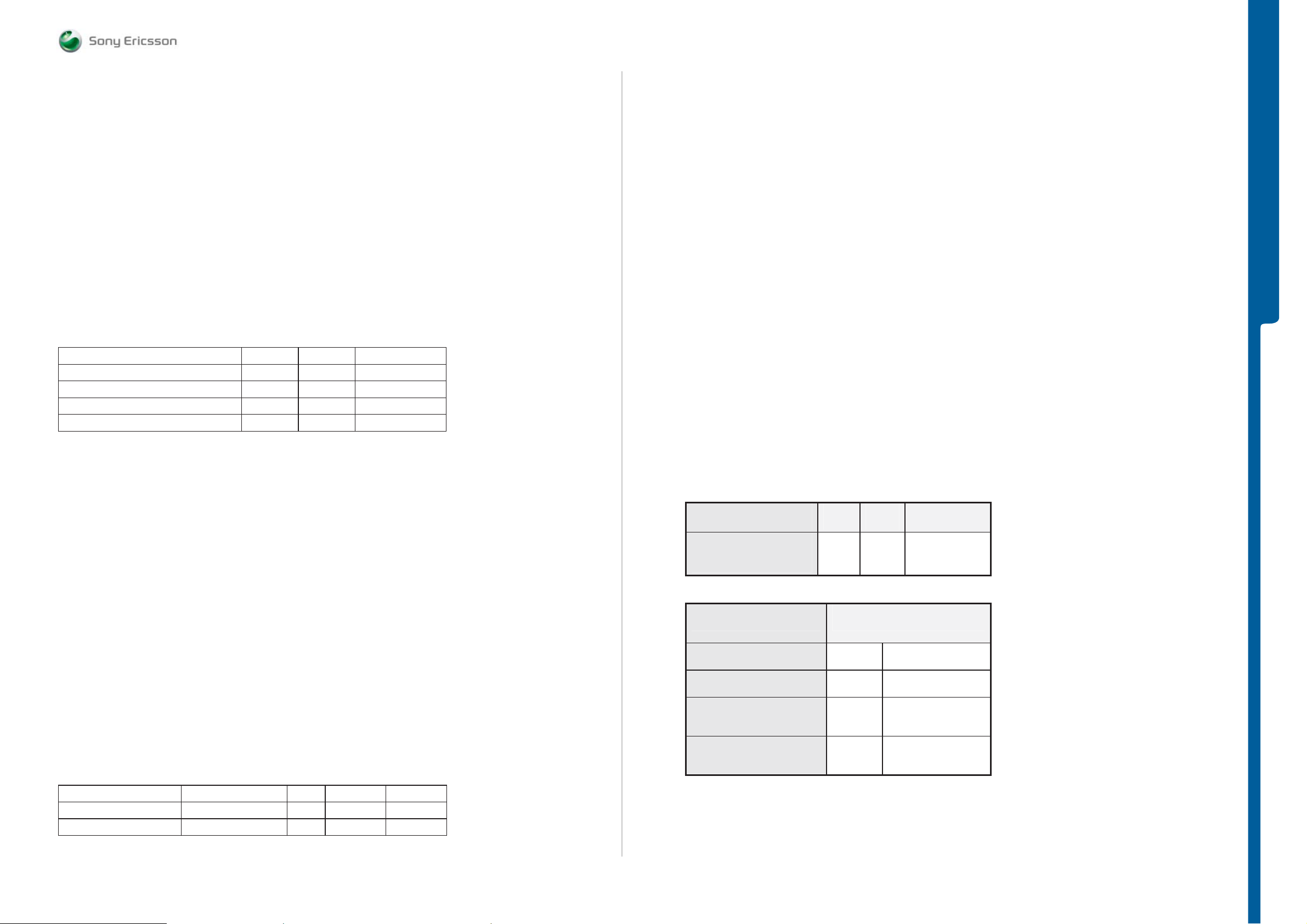
Limits Table for the Battery Calibration Test
Voltage Level on VBATT Min Max UNIT
3.2 Volt
3.2 Volt
4.1 Volt
4.1 Volt
Instrument settings for the Current Calibration Test
202 338 mV
CA 152 HEX
743 886 mV
2E7 376 HEX
Backup Capacitor Test
To perform this test use:
- Phone with the ITP SW
- Power Supply Channel 1 VBATT: Instrument settings: Voltage: 3.8V, Limiter: 2A
- Power Supply Channel 2 DCIO/SEPI: Instrument settings Voltage: 5V, Limiter: 2A
This test should be preformed in 3 steps:
Step1:
Measure the voltage at the Back up capacitor by using Fault Trace SW- Logic ADC Values – Read ADC Value (Reading 1).
Step2:
This step should be done 30 seconds after Step 1. Measure the voltage at the
Backup capacitor by using Fault Trace SW - Logic – ADC Values - ADC Channels
– Read ADC Value (Reading 2).
Step3:
Compare the difference between Reading 1 and Reading 2 with the reference table
below. If the Reading 1 value is between 50 and 680 go to Interval 1, if between 681
and 800 go to Interval 2, if between 801 and 880 go to Interval 3 and compare with
the Reading 2 – Reading 1 Min and Max Limits.
TROUBLESHOOTING
If test is performed at the Core Level then use dummy battery according to the K850
Equipment List for this test. If using TRS Fixture no dummy battery is needed.
Note: The Power Supply Channel 1 VBATT must allow reverse current.
Note: Maximal cable length between Power Supply Channel 1 VBATT and the dummy
battery or TRS Fixture must be 1m. The cable must have a capacity for at least 16A.
Note: Length of the Power Supply Channel 2 DCIO/SEPI customized cable must be
exact 1,3m.
Power Supply Channel 1 VBATT:
3.8 Volt
Limiter 2A
Power Supply Channel 2 DCIO/SEPI:
5.0 Volt
Limiter: 2A
Limits Table for the Current Calibration Test
Measured Current Name Min Max Unit
100mA
800mA
DCIO Current 50 150 mA
DCIO Current 725 875 mA
Reference Table:
Min Max Unit
Absolute readout
Reading 1
Reading 1 (Dec) Reading 2–Reading 1 (Dec)
Interval 1 (50 – 680)
Interval 2 (681 – 800)
Interval 3 (801 – 880)
Note: The upper table contains the absolute limits for the readouts. The lower table
contains the allowed delta between the first and the second readout, separated in
time with 30 seconds.
50 880 Dec
Min Max
20 210
530
010
If the readings is out of limits replace C2217 Backup capacitor.
If problem is not solved then SL 5 Replace N2000 SL 4 Scrap.
1203-2528 rev. 1
22 (101)
TROUBLESHOOTING Test Charging
/ ASIC Revision Test
SEMC Troubleshooting Manual
K850
To perform this test use:
- Phone with the Normal SW (SSW)
- Dummy Battery connected to Power Supply Channel 1 VBATT
- Power Supply Channel 1 VBATT instrument settings:
Voltage: 3.0 to 4.2 Volts, according to VBATT row in the Reference Table.
Limiter: 2A
- Power Supply Channel 2 DCIO/SEPI instrument settings:
Voltage: 5V
Limiter: 2A
Test instructions:
- Disconnect the DCIO/SEPI Cable between each measurement and wait phone
- Take a note of Current measurements at Power Supply Channel 2 DCIO/SEPI
- Compare test results with reference table below, tolerance +/-20%.
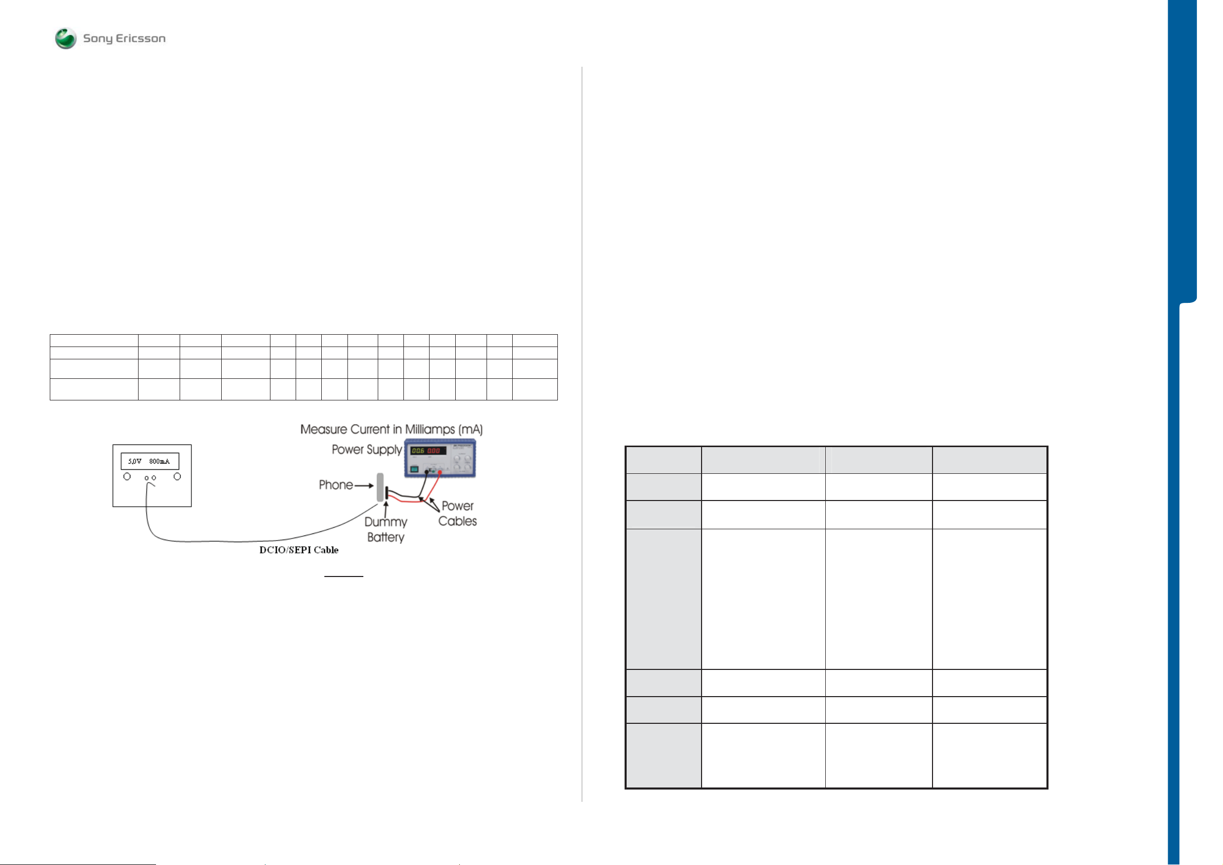
Reference Table
VBATT x Volt
Test Time x sec.
DCIO/SEPI Current
mA
Display indicate
charging
Test Charging
to shutdown when changing VBATT voltage.
and Display charging indicator status, X seconds after DCIO/SEPI cable has
been inserted according to Test Time row in the reference table below.
3.0 3.1 3.2 3.3 3.4 3.5 3.6 3.7 3.8 3.9 4.0 4.1 4.2
15s 15s 25s 25s 25s 25s 25s 25s 25s 25s 25s 25s 35s
200 200 200-400 200 200 200 200 750 750 750 650 380 0
Nothing Nothing Yes Yes Yes Yes Yes Yes Yes Yes Yes Yes
Fully
Charged
ASIC Revision Test
Purpose with this test is to check following items:
- that ASIC-s Revision State is correct
- Check if communication to and from the ASIC-s is Ok
TROUBLESHOOTING
The following ASIC-s is tested:
- D2000 (Anja)
- N2000 (Vera)
- N1400 (Bluetooth and FM Radio ASIC)
- N2525 (Accelerometer)
- Touchpad ASIC
To perform this test use:
- Phone with the ITP SW
- TRS Fixture
- Power Supply Channel 1 VBATT (Voltage: 3.8V, Limiter: 2A)
- Power supply Channel 2 DCIO/SEPI (Voltage: 5V, Limiter: 2A)
- Fault Trace SW choose General – Asic Revisions – Read All
Power Supply Channel 1 VBATT must allow reverse current.
If the charging current is Not equal to the reference table go to Charging probl ems
TRS Guide.
If the charging current is equal to reference table then insert the normal battery and
test the charging current to define if the phone battery is working properly.
Measure the voltage at the battery to define the current level.
If the battery is receiving the right current, then the phone and the battery are
working properly.
Reference returned value can be found in the table below.
ASIC Description Product number Return value (hex)
D2000
N2000
N1400
N1400
N2525
Anja 1200-0795 0x2C8
Vera 1000-8142 0xC5
Bluetooth:
Firmware Revision
Chip ID
1200-6182
Ox5,0x1
0x0,0x0,0x0,0x0
Will always return 0
on STLC because
Chip ID is not
supported.
FM Radio 1200-6182 Ox800
Accelerometer 1200-1223 0x3B
Touchpad
ASIC
Touchpad
1200-1603 0x1975
Will always return
0xFFFF on PBA level
1203-2528 rev. 1
23 (101)
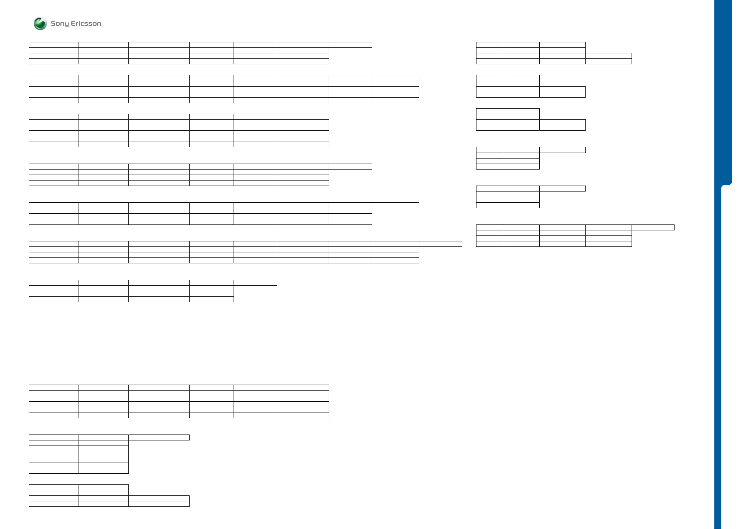
TROUBLESHOOTING Reference Measurement Points
-
Voltages to N2000 Clocks to N2000
MP MP PBA GND MP 79 (X2200 Pin 3) MP 31 (TP2200) MP 29 (TP2202) MP 48 (C2242) Power sup 3.80 V MP MP 85 (C2116) MP 6 (B2101_Pin7)
GND VBAT VBATI BDATA VDD_REF SYSCLK1/MCLK RTCCLK
Phone Off 0.00V 3.8V 3.8V 0.00V 3.8V Phone Off 0Hz 32.768kHz Power sup 0.00 Volt
Phone On 0.00V 3.8V 3.8V 0.00V 3.8V Phone On 26MHz 32.768kHz Power sup 3.80 Volt
Voltages from N2000 Clocks from N2000
MP MP 17 (ST2204) MP 11 (ST2203) MP 9 (ST2208) MP 14 (ST2212) MP 34 (ST2213) MP 36 (ST2214) MP MP 21 (R2125)
VAUDIO26 VANA25 VDDE18 VBT27 VDIG VBEAR26 RTCCLK
0.00V 0.00V 0.00V 0.00V 0.00V 0.00V Power sup 0.00 Volt Phone Off 0Hz Power sup 3.80 Volt
Phone Off 0.00V 0.00V 0.00V 0.00V 0.00V 0.00V Power sup 3.80 Volt Phone On 32.768kHz Power sup 3.80 Volt
Phone On 2.6V 2.5V 1.8V 2.7V 2.7V 2.6V Power sup 3.80 Volt
VCORE18 from N2202
Voltages from N2000 MP MP 158 (ST2217)
MP MP 56 (ST2206) MP 12 (ST2215) MP 7 (C2218) MP 22 (ST2210) VCORE18
VCORE12 VccA VDD_LP VBACKUP Phone Off 0.00V Power sup 0.00 Volt
0.00V 0.00V 2.2V 2.2V Power sup 0.00 Volt Phone On 1.8V Power sup 3.80 Volt
Phone Off 0.00V 0.00V 2.2V 2.2V Power sup 3.80 Volt
Phone On 1.2V 2.8V 2.2V 2.2V Power sup 3.80 Volt Memory Card
C2217 Completely charged Memory Card inserted and Combo Reader connected to the PBA
MP MP 16 (ST2202) Power sup 3.80 Volt
WCDMA N1210 VMC28
Use Fault Trace SW to activate and deactivate WCDMA Radio Phone Off 0.00V
MP MP 84 (L2207) MP 83 (R2221) MP 81 (R2220) MP 12 (ST2215) MP 9 (ST2208) Power sup 3.80 Volt Phone On 2.8V
VCC_WPA WPAVCC DCDC_EN VccA VDDE18
WCDMA Radio Off 0.00V 0.00V 0.00V 2.8V 1.8V Red LED V2428
WCDMA Radio On 3.4V 1.4V 1.8V 2.8V 1.8V Use Fault Trace SW to activate and deactivate Red LED
MP MP 128 (C2427) Power sup 3.80 Volt
Bluetooth N1400 REDLED
Use Fault Trace SW to activate and deactivate Bluetooth REDLED Off 0.00V
MP MP 147 (ST1404) MP 143 (C1408) MP 146 (C1409) MP150 (C1412) MP 148 (R2118) MP 21 (R2125) Power sup 3.80 Volt REDLED On 1.8V
VDIG VDDE18 VBT27 VDDE18 BT_CLK RTCCLK
Bluetooth Off 2.7V 1.8V 2.7V 1.8V 26MHz 32.768kHz FM Radio N1400
Bluetooth On 2.7V 1.8V 2.7V 1.8V 26MHz 32.768kHz Use Fault Trace SW to activate and deactivate FM Radio
MP MP 151 (ST2282) MP 154 (C3305) MP 152 (R3301) Power sup 3.80 Volt
Main Camera VBATI VDDE18 RTCCLK
Use Fault Trace SW to activate and deactivate Main Camera. Display and Main Camera module must be connected to the PBA FM Radio Off 3.8V 1.8V 32.768kHz
MP MP 76 (R2280) MP 27 (TP2206) MP 28 (TP2207) MP 32 (TP2204) MP 82 (ST2275) MP 54 (TP2208) MP 77 (R4301) Power sup 3.80 Volt FM Radio On 3.8V 1.8V 32.768kHz
CAM_LDO_EN VCAMIO VCAML VCAMAF VCAMSA VCAMSD CAMSYSCLK/MCLK
Main Camera Off 0.00V 0.00V 0.00V 0.00V 0.00V 0.00V 0Hz
Main Camera On 1.8V 1.8V 1.2V 2.8V 2.8V 1.8V 26MHz
SEMC Troubleshooting Manual
K850
TROUBLESHOOTING
VGA Camera
Use Fault Trace SW to activate and deactivate VGA Camera. Display and VGA Camera must be connected to the PBA
MP MP 27 (TP2206) MP 82 (ST2275) MP 77 (R4301) Power sup 3.80 Volt
VGA Camera Off 0.00V 0.00V 0Hz
VGA Camera On 1.8V 2.8V 13MHz
Charging
Charging off 1:
DCIO/SEPI not
connected.
Charging off 2:
DCIO/SEPI connected.
MP MP 40 (C2201) MP 47 (C2241) MP 39 (V2202 Pin2) MP 41 (R2201) Power sup 3.8 Volt
Charging off 1 0.00V 3.6V 3.2V 3.8V Charger voltage 0.0 Volt
Charging off 2 5.0V 4.7V 4.7V 3.8V Charger voltage 5.0 Volt
Charging 100mA 5.0V 4.7V 4.7V 3.8V Charger voltage 5.0 Volt
Charging 800mA 4.5V 4.4V 2.8V 4.2V Charger voltage 5.0 Volt
VBUS
USB cable connected to PC
MP MP 44 (ST2201) Power sup 3.80 Volt
USB Cable disonnected
from the phone
USB Cable connected to
the phone
VCAMIO VCAMSA CAMSYSCLK/MCLK
Charging 100mA:
Use Fault Trace SW:
Start Current Calibration
> Set VBATT to 3.8
Note: The Current
Calibration Test must be
repeated if current
consumption goes below
50mA at Power Supply
Channel 2 when you are
performing this
measurements.
DCIO DCIO_INT CHREG CHSENSEP
VBUS
0.00V
5.0V
Charging 800mA:
Use Fault Trace SW:
Start Current Calibration ->
Set VBATT to 3.8V ->
Perform Step1 Note: The
Current Calibration Test must
be repeted if current
consumtion goes below
725mA at Power Supply
Channel 2 when you are
performing this
measurements.
MCLK 26MHz from N1200
MP MP 149 (R2100)
MCLK
Phone Off 0Hz Power sup 3.80 Volt
Phone On 26MHz Power sup 3.80 Volt
1203-2528 rev. 1
24 (101)
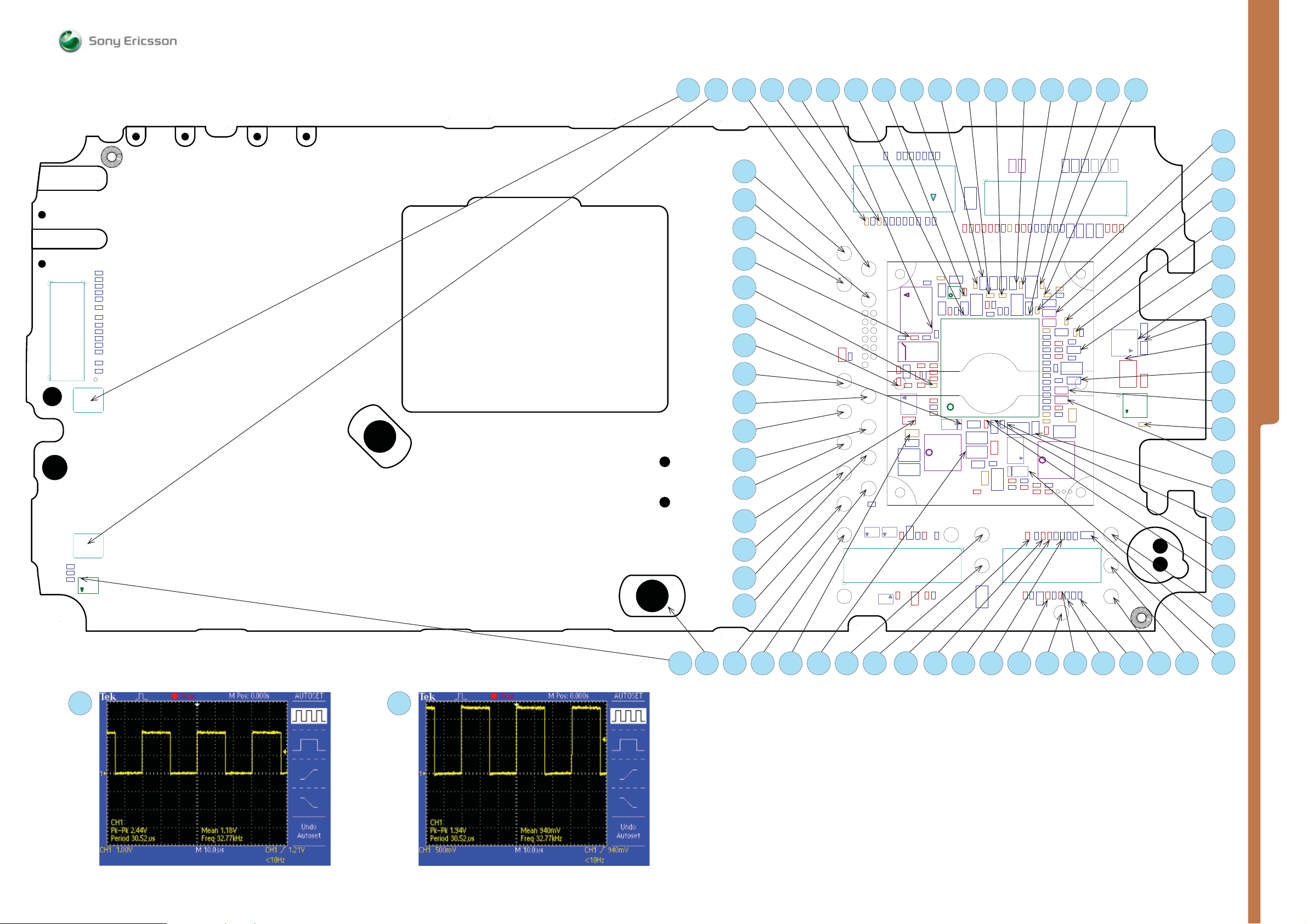
A1
B1
X4300
X3100
X3101
C4210
C4209
C4208
N4200
C4343
C4342
C4341
C4340
C4339
C4325
C4330
C4338
C4337
C4336
C4332
C4328
C4331
C4329
SP4300
MEASUREMENT POINTS Front Side
MP 18
MP 19
MP 20
MP 21
MP 22
MP 23
MP 24
MP 25
MP 26
MP 27
MP 28
MP 29
MP 30
MP 31
MP 32
MP 33
TP4112
TP4106
TP4201
TP2206
TP2202
TP2200
TP2201
TP2502
TP2503
R2443
SP5110
SP5114
SP5116
SP5112
SP5115
C2432
SP5118
ST4201
TP2203
TP3100
SP5111
TP4200
TP2207
TP2204
TP2208
C2293
V2511
A1
B1
MP 8MP 7MP 6MP 5MP 4MP 3 MP 9 MP 17MP 16MP 15MP 14MP 13MP 12MP 11MP 10MP 1 Mp 2
C4204
26
X4200
25
C4214
C4213
ST4200
SP5119
SP5120
SP5108
SP5117
SP5113
SP5109
V2512
X2511
V2510
C4221
C4222
C4227
C4220
C4228
C4224
C4225
C4226
C4223
C2107
B2101
C2102 C2103
R2125
B2100
R2129
R4206
C4211
R2130
R2427
R2204
R2464
V4205
R2544
ST2206
C2221
C2240
C2222
E1002
C2510
C2508
R2507
R2502
R2517
C4218
C4219
C4217
2
1
C4215
C4216
ST4204
C2223
C2208
C2204
R24103
R2421
C2105
R2422
ST2210
R4209
C4230
R4214
V2207
L2200
C2511
R2543
R2516
C2515
C4233
R2480
R2479
C2224
ST2208
N2201
R2206
C2218
C4229
R2203
N2000
C2220
C2219
L2201
C2226
R3201
TP2504
TP2501
TP2500
R2478
R2477
C2214
C2202
C2507
R2476
R3154
C3154
R4215
C4202
ST4203
C2216
C3138
R4203 C2242
R2475
ST2215ST2203
C2472
C2230
C2207
C2229
C2210
C4203
L2463
ST2457
C2205
C2241
V4200
V4201
R4211
C4231
L2462
R2458
C2459
R2459
ST2212
C2213
C2200
C2215
C4232
R4202
R4212
R3200
R24109
X2409
C2447
R2407
C2453
X2410
C2461
C2464
C2463
C2460
C2462
ST2407
ST2202
C2400
ST2204
C2209
L3105
ST2213
L3106
ST3101
C2225
C3130
C3131
R3158
C3132
C3133
C3127
R3114
C3126
C3112
C3129
C3151
C3152
C3119
C3139
C3140
L3103
C3136
L3104
C3135
C2405
R2416
ST2400
C2429
ST2401
C4200
C2406
R2419
L4201
C4201
R3203
SP3204
SP3205
C2448
C2407
R24108
R24107
R24106
C2445
R24110
R24105
C2446
TP2402
SEMC Troubleshooting Manual
V2466
V2467
V2465
C2452
C2454
A1
B1
R2468
R2469
C2456
C2455
SP2419
TP2400
TP2403
TP2401
R2467
V2202
N2402
R2201
ST2201
C2424
C2201
R2483
ST2214
C3122
C3137
C3102
C3160
C2409
C2408
C2450
ST4202
SP2407
C2428
C2451
C3121
ST3100
C2411
C2440
A1
B1
C2410
K850
MP 34
MP 35
MP 36
MP 37
MP 38
MP 39
MP 40
MP 41
MP 42
MP 43
MP 44
MP 45
MP 46
MP 47
MP 48
MP 49
MP 50
MEASUREMENT POINTS
MP 6
MP 21
Pk-Pk 2.44V Mean 1.18V Period 30.52μs Freq 32.77 kHz Pk-Pk 1.94V Mean 940mV Period 30.52μs Freq 32.77 kHz
MP 66MP 65MP 64MP 63 MP 67 MP 68 MP 70
MP 69MP 52 MP 56MP 55MP 54MP 53 MP 57 MP 59MP 58 MP 62MP 61MP 60
1203-2528 rev. 1
MP 51
MP 71
25 (101)
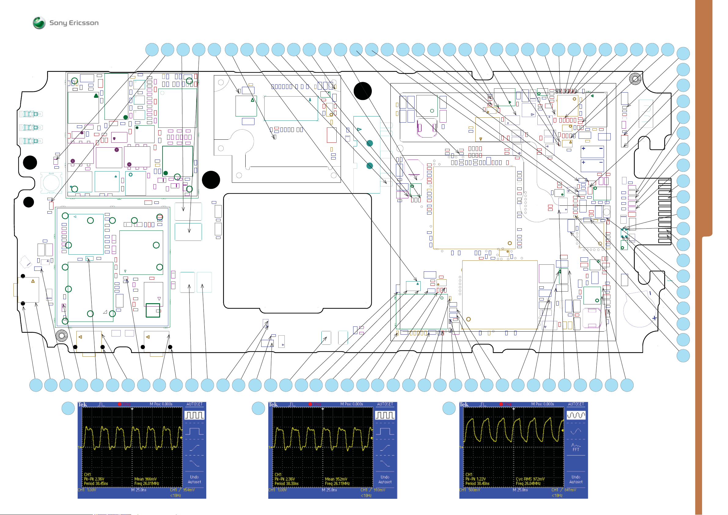
MEASUREMENT POINTS
Back Side
SEMC Troubleshooting Manual
K850
V2428
S2400
C2427
C3142
C3159
L3111
V3100
X1203
X1201
X1202
L1200
OUT
X1200
IN
C1200
R1201
C1203
L3110
C3141
V2402
C2426
MP 86 MP MP 85
L211
C201
1R
0
00
0201C
V2478
ST304
C330C409
C405
C328
L310
R400 C411
2011L
L1005
R1014
C410
Z302
C324
Z300
C333
Z301
C325 C335
K400
Z201
3011L
N1001
8
101C
9101C
2101R
101R
3
C
329
C332
C331
L317
L308
L325
L324
L309
L313
L327
L326
N401
L213
R2442
R1100
C1117
S2402
ST300
L204
C2431
C1116
5011R
B1100
L316
R311
R312
R313
L312
R407
C414
R406
C308
C313
C334
L203
11C
R
4
011
C311
ST301
C315
C312
N300
L303 L305L301
L321
L302
N301
L205
L201
1011R
91
8111C
C319
L320
L200
C413
C318
C317
C316
C320
L323
L322
L300
X3102
X3103
L4203
L4202
C314
ST303
L319
L318
L304
C203L202
L206
L207
X2506
R302
R310
C307
C306
E100
C3108
C3109
C3107
X2507
L3108
L3109
ST2280
C2281
R2280
N2206
C2280
V3101
C4206
C4306
C4313
C4351
X4301
R4310
C4327
C4305
C4326
R4301
C4207
V4203
C4310
C4308
C4312
C4350
C4311
C4309
C4307
E1001
C4321
C4320
C4314
C4315
C2291
C2292
C2290
N2208
R2290
R4316
C4352
S4300
ST2218
R2200
ST2219
C2211
C2212
ST2275
C2275
R2286
R4315
C2244
V2200
X2200
E1000
C2284
ST2283 ST2284
C2286
C2237
C2236
L2207
C2235
C2234
C2233
N2205
L2210
C2232
Z1400
C1408
ST2276
N1400
X1400
X1401
C1402
L1402
L1401
C1407
ST1404
C403
C418
C408
C407
C404
ST305
C417
C321
R402
C406
C402
C420
N400
N402
C400
C416
L400
K404
C415
R408
C1202
K403
C1201
1C
000
0001L
0
01L
1
2001C
1C
300
L
0
1
20
6101C
4001L
Z200
L212
L209
200
C
Z1000
1001Z
2101C
N1200
C1015C1014
L1006
N1002
S2403
C401
C419
R411
R410
R404
R405
R403
Z202
L210
C202
4111C
3111C
0111C
1C
901
2011C
C
1
1
10
C
1
0
1
6
5011C
3101C
R401
K402
N1210
K401
L1101 L1100
R1006
R1005
R1007
4001C
C
001
5
C
1
001
C1006
7101C
V2477
C2287 C2285
R2220
SP3209
ST1403
ST1402
N2203
L2261
SP3208
C2231
R2221
SP2136
ST3300
ST1400
SP2125
SP2122
R2402
R2401
C2311
C2307
R2404
R2403
ST2241
C2340
C2318
R3202
C2339
R2551
C2322
C2336
C2121
C1409
C1412
ST1406
MP 90 MP 91 MP 98MP 97MP 92
C2283L2260
C2282
R2115
R2116
C2116
C2115
SP2124
C2110
SP2105
SP2103
C2325
C2334
R2104
C5102
D2000
C2315
C2302
SP5101
R2101
R2121
D2105
R2119
R2118
C3302
C2314
C2335
SP2114
SP2112
SP2111
SP2116
SP2113
R2100
R2120
SP2130
ST2282
C3304
C3145
C3146
R3302
C3305
C3306
L3300
R3301
SP2123
SP2101
C2328
ST2405
C2550
R1215R1209
R1210 R1214
C2324
C2329
C5100
MP 94MP 93 MP 95 MP 96
C2509
R2500
R4304
D4300
R4300
D2420
R1217R1207
R1216
R1208
C2352
C2104
C2326
R1206
SP2106
C2316
C2333
C2304
C2342
C2345R2126
D2010
SP2109
C2350
ST2105
N2500
R4305
R2534
R3153
R2506
R2520
C2330
C2327
SP2108
SP2115
D2011
SP2135
SP2120
SP2126
C2346
V2505
R2505
R1203
SP2110
V2507
V2506
V2501
R2521
SP2107
SP2118
C2344
MP 105MP 104MP 103MP 102MP 101MP 100MP 99MP 89MP 78MP 77 MP 8887MP 84MP 83MP 82MP 81MP 80MP 79MP 76MP 75MP 74MP 73MP 72
MP 106
MP 107
R2513
N2503
V2515
C2501
V2500
C2504
C2503
R2510
R2524
C2502
SP2410
SP2408
C2500
R2537
V2504
V2503
R2508
R2504
V2502
R2503
V2513
R2522
C2308
C2305
C2341
ST1401
C2319
SP2137
R2485
SP5103
R5101
SP5107
C2317
SP5102
SP5104
SP5106
SP5105
C2353
C2338
C2303
C2337
C2313
R5100
C2301
SP2127
L2203
C2347
C2348
ST2217
C2351
C2349
V2231
SP2117
SP2129
V2206
SP2128
C2343
R2448
R2446
C2526
R2447
R2496
R2445
R2444
C2505
R2511
R2512
D2460
R2535
R2491
R2509
R24102
R2523
R2490
D2405
R2499
D2410
ST2406
C2403
N2525
C2402
R2498
R2494
R2492
R2493
R24101
C2470
R2497
R2495
C2525
R2406
C2471
R24100
C2401
C2524
ST2506
ST2505
C3149
R2550
C2422
R3109
C3117
R3155
C3110
C3111
C3118
X3105
L3100
R2470
C3150
R3129
R3131
R2433
R2484
SP2403
R3130
C3114
ST2429
SP2414
N3100
L3125
N3101
C3115
C2433
C2475
SP2411
SP2413
SP2412
R3157
R3103
C3106
R3106
R3115
R4116
R4114
L4112
R3128
C3116
C2476
R2465
R2466
R2426
C2413
ST2428
R3102
C4111
C4109
C4108
R2486
R4115
C4110
L3124
V2425
C2421
C2420
C2416
C2415
V2420
Z2450
C2423
C2434
L2405
L2401
L2402
L2403
L2404
R2451
R2455
V2421
N2401
C2217
V2405
R2207
ST4103
V2406
C2474
SP2404
SP2418
SP2417
SP2416
SPSP2415
N2202
C4103
C4102
ST4101
ST4102
R2436
R2440
R2439
C2425
R2441
ST2441
SP2409
C2473
C4120
R4101
C3155
C3125
R3112
C3124
C3156
C3103
R3116
C4122
R4102
C4105
C4101
C3157R3156
C3158
C2414
D2404
C3105
R4103
C4107
N4101
L4105
R2473
R2435
N2400
C2430
R2437
R2438
C2239
C2243
C4104
R2231
MP 108
MP 109
MP 110
MP 111
MP 112
MP 113
MP 114
MP 115
MP 116
MP 117
MP 118
MP 119
MP 120
MP 121
MP 122
MP 123
MEASUREMENT POINTS
MP 124
MP 125
MP 133MP 132MP 131MP 130MP 129MP 128 MP 134 MP 155MP 154MP 153MP 152 MP 156 MP 164MP 163MP 162MP 161MP 160MP 159MP 157MP 127 MP 158MP 141MP 140MP 138MP 137MP 136MP 135 MP 139 MP 151MP 150MP 149MP 148MP 147MP 146MP 145MP 144MP 143MP 142MP 126
MP 85 MP 148 MP 149
Pk-Pk 2.36V Mean 966mV Period 38.45ns Freq 26.01MHz Pk-Pk 2.36V Mean 952mV Period 38.30ns Freq 26.11MHz Pk-Pk 1.22V Mean 972mV Period 38.40ns Freq 26.04MHz
1203-2528 rev. 1
26 (101)
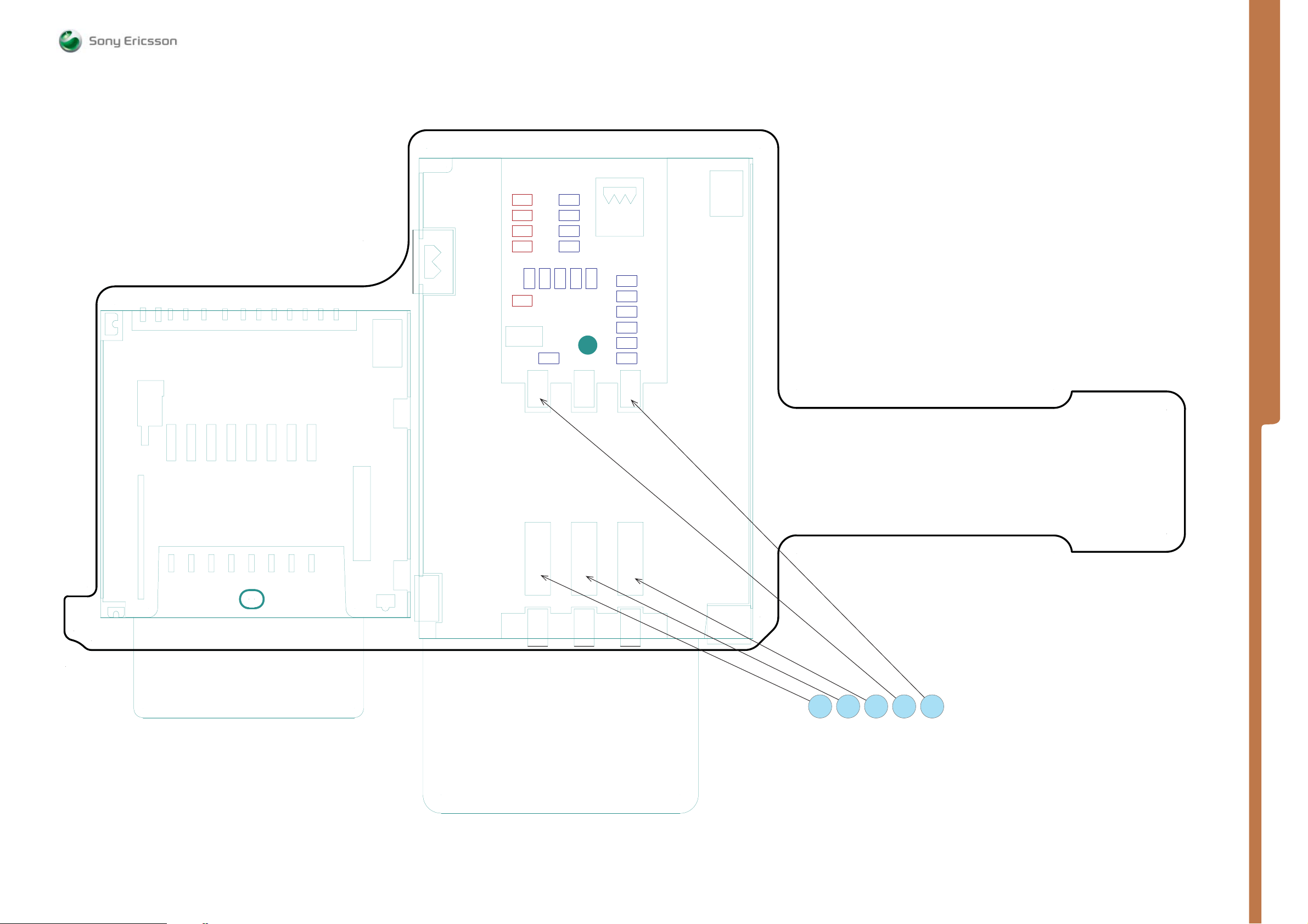
MEASUREMENT POINTS SIM & Memory Card Holder
SEMC Troubleshooting Manual
K850
X1001
C1004
C1003
C1013
C1008
C1007
C1006
C1005
C1002
C1000
R1000
R1003
R1004
R1002
R1001
756
X1002
C1114
C1009
C1115
C1010
C1001
C1011
C1012
MEASUREMENT POINTS
MEMORY CARD
SIM CARD
123
MPSIM3 MPSIM5MPSIM7MPSIM1MPSIM2
1203-2528 rev. 1
27 (101)
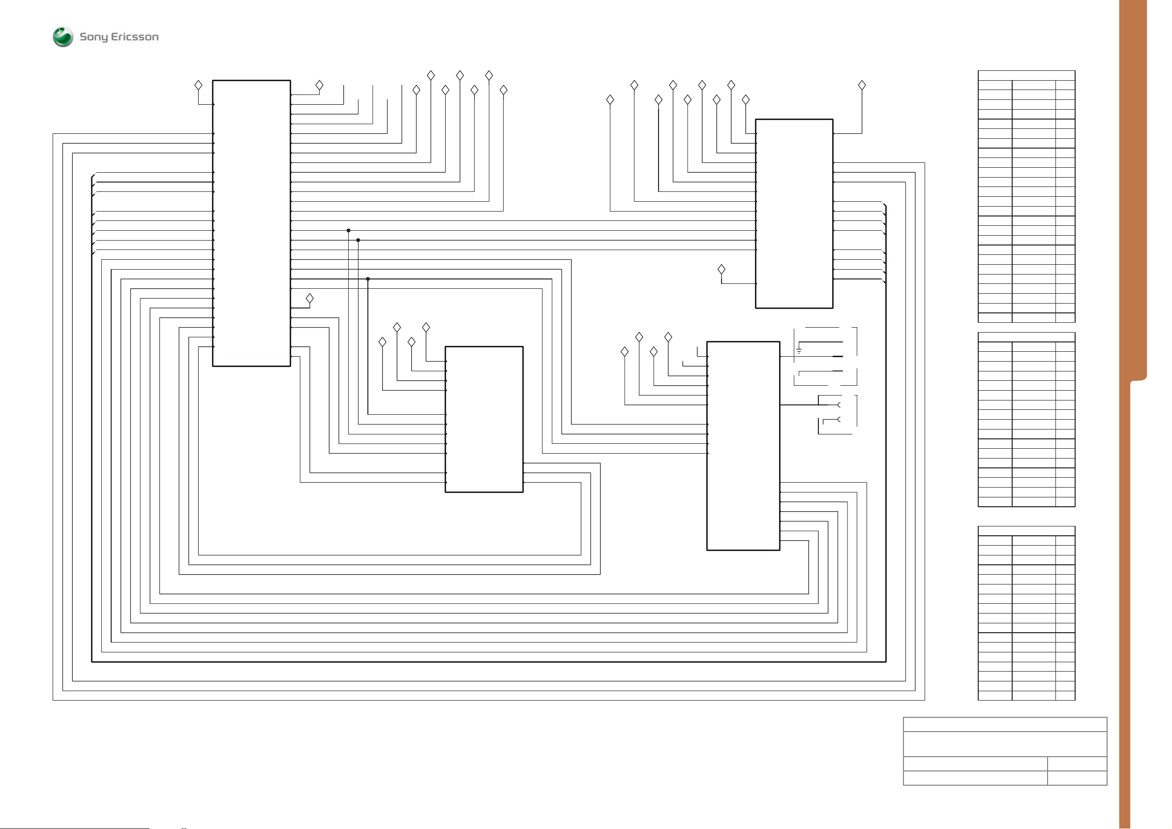
LED_ROW1
LED_ROW2
LED_ROW3
LED_CAMERA
LED_VIDEO
LED_PLAY
AF_LED
LED_BACK
STEPUP50
CC
OPTOSENSE
FLASH_STROBE
LD_AD
MCLK
TX_ADSTR
DCDC_EN
TESTOUT
WPAVCC
BT_CLKREQ
VAD
SPL
SPR
Application & Sys.Performance
Application & Sys.Performance
LED_ROW1
LED_ROW2
LED_ROW3
LED_CAMERA
LED_VIDEO
LED_PLAY
AF_LED
LED_BACK
VCAMAF
VBATISTEPUP50
VDDE18
VDIG
VccA
VCC_WPA
VBT27
VAUDIO26
VBEAR26
VOPTO30
VCAML
VCAMSA
VCAMIO
VCAMSD
I2CCLK1
I2CDAT1
CAMSYSCLK
MCLKREQ
BT_CLK
RTCCLK
BTRESn
CAM_LDO_EN
MICN/AUXinR
MICP/AUXin L
FMRESn
FM_ANTENNA
VCAMAF
CAM_LDO_EN
VBATI
VDDE18
VDIG
VccA
VAUDIO26
VBEAR26
MEASUREMENT POINTS Sofi a Top Schematic
VCC_WPA VAUDIO26
VBT27
VCAMSD
I2CCLK1
I2CDAT1
CAMSYSCLK
MCLKREQ
BT_CLK
RTCCLK
BTRESn
VBATI
VDDE18
MICN/AUXinR
MICP/AUXinL
FMRESn
FM_ANTENNA
VOPTO30 VCAMSA
VBEAR26
VBATI
VDDE18
VAUDIO26
VBEAR26
RTCCLK
I2CDAT1
I2CCLK1
MICN/AUXinR
MICP/AUXinL
FMRESn
FM_ANTENNA
Audio
Audio
VCAML VCAMIO
VAD
SPL
SPR
SPR
SPL
VAD
BT_CLKREQ
WPAVCC
TESTOUT
DCDC_EN
TX_ADSTR
MCLK
LD_AD
LEDS
FLASH_STROBE
OPTOSENSE
CC
VCAML
VAUDIO26
VBT27
VCAMIO
VccA
VCC_WPAVDIG
VCAMAF
VDDE18
VDIGVCAMSA
VBATI
VDDE18
VOPTO30
CAM_LDO_EN
VBATI
VDDE18
VccA
VCC_WPA
VBT27
VDIG
MCLKREQ
BT_CLK
RTCCLK
BTRESn
Access
Access
VBATI
VBATI
VDDE18
VOPTO30
VDIG
VCAMAF
VCAMSA
VCAMIO
VAUDIO26
VCAML
VCAMSD
I2CCLK1
I2CDAT1
CAMSYSCLK
CAM_LDO_EN
Imaging
Imaging
ANT
BT_ANT
LD_AD
MCLK
TX_ADSTR
DCDC_EN
TESTOUT
WPAVCC
BT_CLKREQ
STEPUP50
OPTOSENSE
FLASH_STROBE
LED_ROW1
LED_ROW2
LED_ROW3
LED_BACK
LED_CAMERA
LED_VIDEO
LED_PLAY
AF_LED
CC
X1203
X1201
X1202
GSM/UMTS
X1400
1
X1401
1
BT
STEPUP50
LED_ROW1
LED_ROW2
LED_ROW3
LED_BACK
LED_CAMERA
LED_VIDEO
LED_PLAY
AF_LED
1
1
1
SEMC Troubleshooting Manual
Access side GPIO mapping
UsagePort
USB_HSSTP
USB_HSDIR
CTMS
CFMS
USB_HS_INCLK
USB_HSNXT
USB_HSDATA4
USB_HSDATA5
USB_HSDATA6
USB_HSDATA7
not used
not used
not used
ResetAC
ModeKey1
ModeKey2
USB_HSCHIP_SEL
ModeKey3
USB_HSDATA3
BT_SPI_CS0n
BT_SPI_DI
BT_SPI_DO
BT_SPI_CLK
USB_HSOUTCLK
Application side GPIO mapping
Port Usage
FM_INT
AP110_INT
CAMIRQ
PSoC_INT
PSoC_RES
CARDDETECT
not used
GPIO_RST
not used
not used
X_CHARGE_RDY
MC_CLK_RET
MSDETECT
AX_INT1
AX_INT2
DCON
GPIO expander mapping
UsagePort
CIF_STANDBY
GPIO_O0
AFLEDEnable
GPIO_O1
AMPCTRL
GPIO_O6
GPIO_O7
MOTOR_LDO
CAM_LDO_EN
GPIO_O8
CAMRESn
GPIO_O9
uSD_bypass_option
GPIO_O10
CAM_LDO2_EN
GPIO_O11
GPIO_O12
X_CHARE_EN
GPIO_O13
SPD1
GPIO_O14
SB
GPIO_O15
SPD0
GPIO_P2 MOTOR_DOOR1
GPIO_P3 MOTOR_DOOR2
GPIO_P4 MOTOR_CW
GPIO_P5 MOTOR_CCW
AP110_SPI_CS
AccGPIO00
AccGPIO01
AccGPIO02
AccGPIO03
AccGPIO04
AccGPIO05
AccGPIO06
AccGPIO07
AccGPIO08
AccGPIO09
AccGPIO10
AccGPIO11
AccGPIO12
AccGPIO13
AccGPIO14
AccGPIO15
AccGPIO16
AccGPIO17
AccGPIO18
AccGPIO19
AccGPIO20
AccGPIO21
AccGPIO22
AccGPIO23
AppGPIO00
AppGPIO01
AppGPIO02
AppGPIO03
AppGPIO04
AppGPIO05
AppGPIO06
AppGPIO07
AppGPIO08
AppGPIO09
AppGPIO10
AppGPIO11
AppGPIO12
AppGPIO13
AppGPIO14
AppGPIO15
K850
MEASUREMENT POINTS
Made for
So a Top Schematic
So a Top
Document Nr Revision
1200-1886 Page 1 3
1203-2528 rev. 1
28 (101)
BT_CLKREQ
MCLK
TESTOUT
LD_AD
VAD
TX_ADSTR
OPTOSENSE
FLASH_STROBE
LED_BACK
LED_ROW1
LED_ROW2
LED_ROW3
LED_CAMERA
LED_VIDEO
LED_PLAY
AF_LED
MEASUREMENT POINTS Application & System Perfor ma nc e Top
APP_LOG
DCON
VDDE18
VCORE18
BT_CLKREQ
MCLK
VAUDIO26
VMC28
VDIG
TESTOUT
LD_AD
VAD
TX_ADSTR
OPTOSENSE
CC
SPL
SPR
FLASH_STROBE
LED_BACK
LED_ROW1
LED_ROW2
LED_ROW3
LED_CAMERA
LED_VIDEO
LED_PLAY
AF_LED
VBACKUP
VBATI
SYSCLK2
DCON
VBATI
VDIG
VDDE18
VMC28
VAUDIO26
STEPUP50
APP_LOG
TESTOUT
LD_AD
VAD
OPTOSENSE
CC
SPL
SPR
FLASH_STROBE
LED_BACK
LED_ROW1
LED_ROW2
LED_ROW3
LED_CAMERA
LED_VIDEO
LED_PLAY
AF_LED
REDLED
SYSCLK2
VBACKUP
Connectivit y
Connectivit y
SERVICEn
ONSWAn
I2CDAT1
I2CCLK1TX_ADSTR
MICN/AUXinR
MICP/AUXinL
FM_ANTENNA
VBUS
DCIO
SERVICEn
ONSWAn
MICN/AUXinR
MICP/AUXinL
VPP
STEPUP50
CC
SPL
SPR
VDDE18
VDD_LP
VCORE18
VDDE18
BT_CLKREQ
MCLK
VDD_LP
SERVICEn FMRESn
ONSWAn
System Control
System Control
APP_LOG
SYSCLK2
CAMSYSCLK
MCLKREQ
DCON
RTCCLK
BT_CLK
BTRESn
SYSCLK2
RTCCLK
BT_CLK
CAMSYSCLK
MCLKREQ
BTRESn
FMRESn
I2CDAT1I2CDAT1
I2CCLK1I2CCLK1
FM_ANTENNAFM_ANTENNA
SEMC Troubleshooting Manual
K850
RTCCLK
BT_CLK
CAMSYSCLK
MCLKREQ
BTRESn
FMRESn
I2CDAT1
I2CCLK1
MICN/AUXinR
MICP/AUXinL
FM_ANTENNA
MEASUREMENT POINTS
WPAVCC
DCDC_EN
STEPUP50
STEPUP50
REDLED
VPP
VBUS
DCIO
WPAVCC
DCDC_EN
VPP
VBUS
DCIO
WPAVCC
DCDC_EN
Power
Power
VCORE18
REDLED
VBACKUP
VMC28
VBATI
VDDE18
VAUDIO26
VBEAR26
VOPTO30
VCAMAF
VCAML
VCAMSA
VCAMIO
VCAMSD
VBT27
VCC_WPA
CAM_LDO_EN
VDD_LP
VMC28
VDDE18
VCORE18
VBACKUP
VDIG
VccA
VDD_LP
VBATI
VDIG
VAUDIO26
VBATI
VDDE18
VDIG
VAUDIO26
VBEAR26
VOPTO30
VCAMAF
VCAML
VCAMSA
VCAMIO
VCAMSD
VBT27
VccA
VCC_WPA
CAM_LDO_EN
VBATI
VDDE18
VDIG
VAUDIO26
VBEAR26
VOPTO30
VCAMAF
VCAML
VCAMSA
VCAMIO
VCAMSD
VBT27
VccA
VCC_WPA
CAM_LDO_EN
Made for
Application & System Performance
Performance & Applications Top
Document Nr Revision
1200-1887 Page 1 3
1203-2528 rev. 1
29 (101)
MEASUREMENT POINTS System Top
VDDE18
SEMC Troubleshooting Manual
K850
MEASUREMENT POINTS
VDD_LP
BT_CLKREQ
MCLK
SERVICEn
ONSWAn
VDD_LP
BT_CLKREQ
MCLK
SERVICEn
ONSWAn
VDDE18
VDD_LP
BT_CLKREQ
MCLK
SERVICEn
ONSWAn
Clocks & Resets
Clocks & Resets
BT_CLK
CAMSYSCLK
RTCCLK
MCLKREQ
DCON
BTRESn
FMRESn
SYSCLK2
MEMRESn
APP_LOG
MEMRESn
VCORE18
VCORE18
MEMRESn
Memories
Memories
APP_LOG
BT_CLK
CAMSYSCLK
RTCCLK
MCLKREQ
DCON
BTRESn
FMRESn
SYSCLK2
BT_CLK
CAMSYSCLK
RTCCLK
MCLKREQ
DCON
BTRESn
FMRESn
SYSCLK2
APP_LOG
Made for
Application & System Performance
System Top
Document Nr Revision
1200-1887 Page 2 3
1203-2528 rev. 1
30 (101)
 Loading...