

Page 1
SEMC Electrical Repair Manual
K800 - K810
ABOUTABOUT FUNCTION OVERVIEW COMPONENT OVERVIEW
Electrical repair manual
K800
K810
SAMPLE POINTS
TROUBLESHOOTER
1202-3085 rev. 2
APPENDIX
1 (121)
Page 2

ABOUT
Contents
SEMC Electrical Repair Manual
K800 - K810
ABOUT
General information
The purpose of this document is to provide enhanced technical information for Sony Ericsson
repair technicians in order to assist during service, repair and troubleshooting operations on Sony
Ericsson mobile phones. It should be used as a complement to other repair instructions and tools
as notifi ed by the local Sony Ericsson representative.
To search for components throughout the entire document use the “search” function in Adobe
Acrobat Reader 7.0 (or later version) and enter the component name or other word. Use zoom to
enlarge.
For easier navigation of the document you can use the bookmarks that appear in the Bookmarks
tab on the left side of the Adobe Acrobat Reader window. Each bookmark jumps to a page in the
document.
Instruments used
Power supply ........................ Agilent 6632B
Power supply………... ...........Agilent 66311B
Power supply set to 3,8V and limited to 2A
Oscilloscope ................ Tektronix TDS 2012
Multimeter ...................................... Fluke 83
Spectrum Analyzer..Hewlett Packard 8596E
Mobile Phone Tester……...Yokogawa VC230
Disclaimer
This document is Sony Ericsson confi dential and should be treated as confi dential in accordance
with the agreement with Sony Ericsson. This document is intended for use by authorized service
technicians only. Sony Ericsson is not to be held responsible for any damages or losses caused
intentionally or unintentionally due to unauthorised use of the information in this document.
Revision Hi st o ry
Rev. Date Changes / Co mments
1 6/29/2007 Initital revision.
CONTENTS
ABOUT 2
General Information 2
Contents 2
FUNCTION OVERVIEW 3
Description 3
General 3
Mechanical Design 3
RF Parts 3
Logic/Audio Part 5
Antenna 5
Bluetooth 5
IR 6
FM Radio 6
External Connections 6
High Level 7
Radio 8
Baseband 9
Data and Signals 10
Acoustics 11
Power Distribution 12
Baseband Top - Radio Top - Bluetooth - FM Radio 13
Radio - Top 14
Radio - Power Supply 15
Radio - UMTS 16
Radio - GSM 17
Radio - Bluetooth 18
Baseband - Logic Top 19
Baseband - System Control Top 20
Baseband - System Control Clocks and Resets 21
Baseband - System Control Test 22
Baseband - Power Top 23
Baseband - Regulators and Charging 24
Baseband - Power Camera 25
Baseband - Power ASICs 26
Baseband - Power Memories 27
Baseband - Operation & Ser vices Top 28
Baseband - Operation & Ser vices Memories 29
Baseband - Operation & Ser vices GPIO 30
Baseband - Operation & Ser vices ADC & DAC 31
Baseband - Operation & Ser vices MS Pico & SIM 32
Baseband - Operation & Ser vices Connectivity 33
Baseband - UMTS Access Top 34
Baseband - UMTS Access WCDMA 35
Baseband - UMTS Access GSM 36
Baseband - MMI Top 37
Baseband - MMI Keypad 38
Baseband - MMI Display 39
Baseband - MMI Audio 40
Baseband - MMI Camera 41
Baseband - MMI FM Radio 42
COMPONENT OVERVIEW 43
Front Side B - C 43
Front Side D - Z 44
Back Side A - Z 45
SAMPLE POINTS 46
Front Side 46
Back Side 47
TROUBLESHOOTER 48
Repair Actions 48
Repair Actions 49
On/Off - Dead Phone 50
Charging Problems - VBUS Charging Problems 51
Keyboard & Display Backlight - SIM 52
Flash Problems - Audio Internal Problems 53
Audio External Problems - Camera Problems 54
FM Radio Problems - Vibrator Problems 55
Memory Stick Problems - Bluetooth Problems 56
Network Problems - Display Problems 57
Test Current Consumptions 58
Tes t Char g i ng 58
Test the ASIC Revisions 59
Test Backup Capacitor 59
Test the Joystick Switch S2504 and Diodes V2503, V2506-09 60
Test the Diode V2500 61
Test the Protection Diodes V2510 to V2514 61
Test the diode V2504 and Switch S2500 62
Test the Switches S2505 & S2506 62
Test the Switch S2502 63
Test the Switches S2503 & S2507 63
Joystick and Other Keys Problems 64
Test the System Connector Protections 64
Reference MP 65
APPENDIX 66
K800 Mechanical Parts List 66
K810 Mechanical Par ts List 70
Part List Main Board 73
Components A1200 74
Components A1300 83
Components B2100, B4100 90
Components C2217, D1400 91
Components D2301, D2304 92
Components H2300, D3100, D3101 93
Components N2000, N2200 94
Components N2202, N2203, N2300 95
Components N2600, N3100, N4100 96
Components N4202, S2500, S2502 97
Components S2504, S2505, S2506 98
Components V2201, V2202 99
Components V2220, V2301, V2552 100
Components V2500, V4101, V2504 101
Components V3101, V3102 102
Components V3103, V3110 103
Components V3113, X1000 104
Components X1002, X2200 105
Components X2301, X2302 106
Components X2501, X2505, X2510 107
Components X2550, X3102 108
Keyboard K800 109
Keyboard K810 110
Display 111
VGA Camera KNC20116 112
Camera Module KNC20125 112
Xenon Flash Module 113
SI Can’t Power On 114
SI Can’t Power On 115
SI Joystick Switch Replacement 116
SI Support Pad for Camera Switch 116
SI Problem with Front Spare Part 117
SI Problem with On/Off Button 117
SI Emma 3 White Screen Patch 118
SIActivate Sporadic Behaviour 118
SI Pre-Confi guration Change 119
SI Vincenne Replacement 120
SI Emma 3 Important Start-Up Operation, SI New Soft ware 120
Tor q ue Se t t ings 121
Placing in a Shield Box 121
ABOUT
1202-3085 rev. 2
2 (121)
Page 3
FUNCT I ON OVERVIEW
Description
SEMC Electrical Repair Manual
K800 - K810
DESCRIPTION
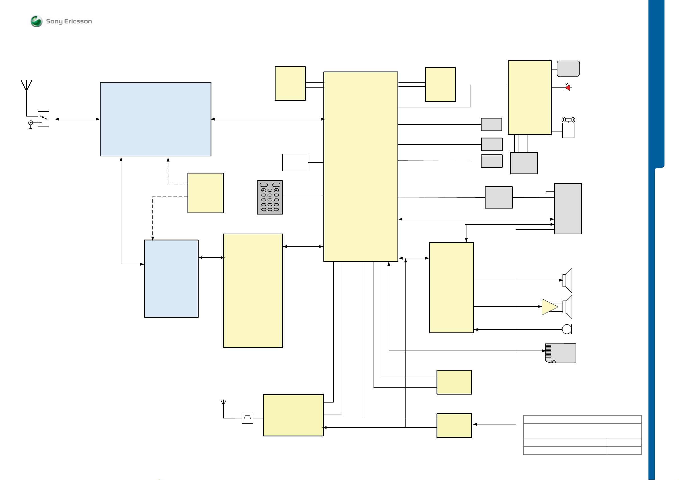
1 General
The Sony Ericsson Mobile Communication phone K800 is a 3G dual mode mobile phone
supporting WCDMA and triple band GSM/GPRS in the 900, 1800 and 1900 frequency bands. The
phone is a GPRS class 10 terminal supporting voice, circuit switched (CS) and packet switched
(PS) data. This Sony Ericsson dual mode 3G product is designed to be compatible with all
mandatory GSM phase 2+ recommendations.
The phone has an in-built antenna, a 3.2 Mega Pixel Camera with a lens cover and an associated
xenon fl ash, a VGA-Camera for Video Call, a Display, and a slot for a Memory Stick M2 external
memory.
There is only one size of battery. A connector at the bottom of the phone makes it possible
to connect various accessories like chargers and hands-free units. A USB cable can also be
connected to the bottom connector. The external antenna connector can be used to connect to an
external antenna, disconnecting the internal phone antenna.
The electronic functions are divided into RF parts, logic/audio parts, opto-electronic parts,
Bluetooth parts, an IR transceiver, and an FM radio. The electronics parts consists of the main
PCB with components placed on both sides, the Key-Flexible-PCB that has Key-Matrix-circuit/
LEDs, loudspeaker box with the internal antenna, ear speaker, microphone, vibrator, 3.2 mega
pixel camera, xenon fl ash module, VGA camera, the Display, Bluetooth module, and FM radio
parts. The RF parts are mainly housed in separate modules.
Antenna
RF Logic / audio
Flash
VGA Camera
2.1 Mechanical Design
The phone is built up around a core unit consisting of a plastic frame with the BT antenna
mounted on which the assembled PCB, the cameras, the vibrator, a plastic LCD holder and
the LCD, a plastic keyboard support plate and the keyboard dome foil, the loud speaker box
with loudspeaker and antenna, and the xenon fl ash module are mounted. This core unit is then
snapped and screwed in the front cover together with the keys, joystick, and the M2 cover. The
antenna cover with the sliding camera lens cover is then mounted. The battery fi ts in a dedicated
cavity and is covered with a battery cover.
Dimensions
Length 106mm
Width 47mm
Thickness 18mm (22mm across the lens cover)
Weight 115g
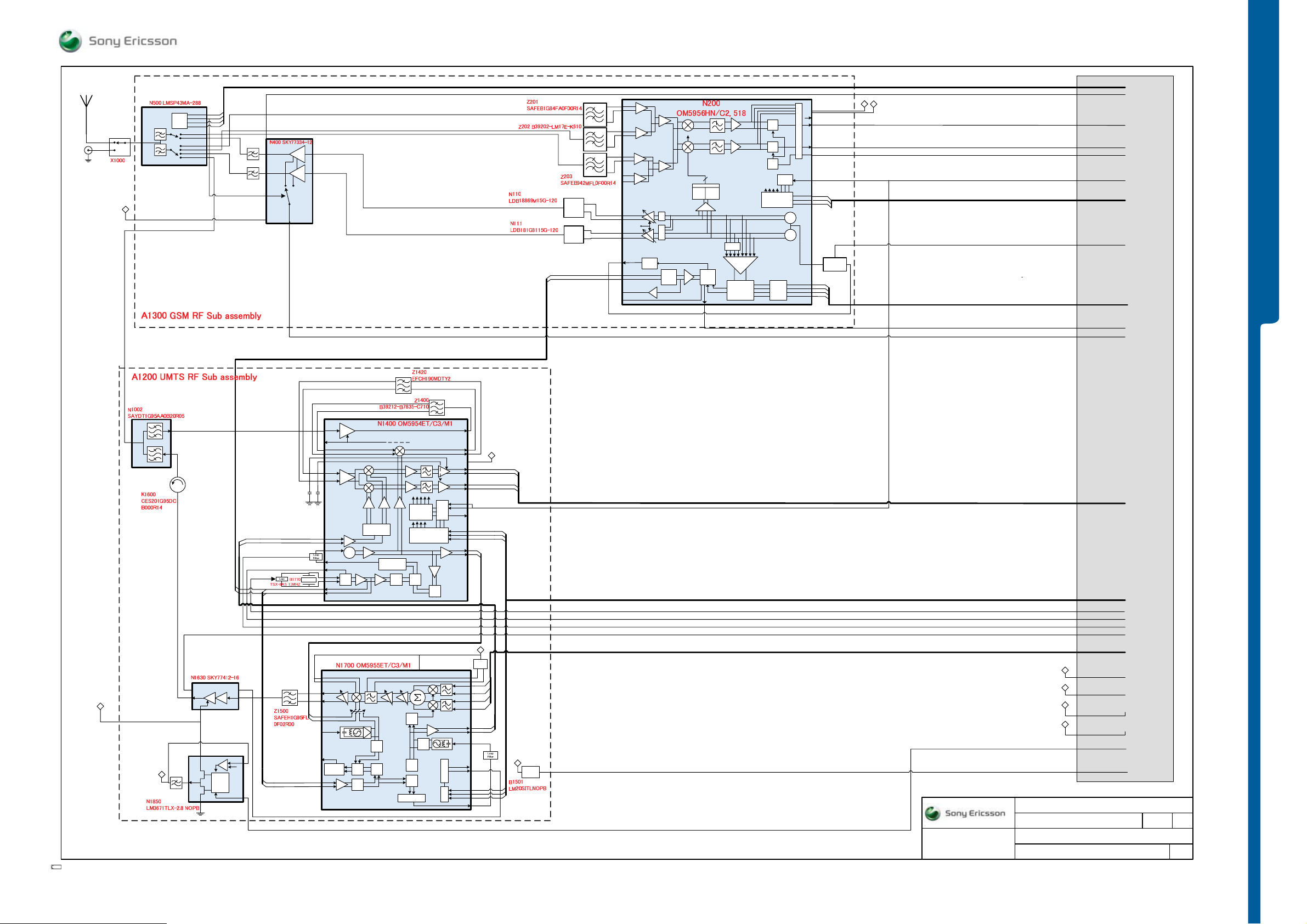
2.2 RF parts
2.2.1 GSM 900
The GSM 900 part of the transceiver is including E-GSM and has a frequency range spanning
from 925.2 to 959.8 MHz for the receiver, and from 880.2 to 914.8 MHz for the transmitter. This
gives 174 channels with 200kHz channel separation. The TX – RX frequency separation is always
45MHz.
2.2.2 GSM 1800
FUNCTION OVERVIEW
3.2 MPix Camera
Transmitter
Receiver
3,6V battery
Figure 1. Block diagram of the K800.
Baseband
Control
DC and Return
Bluetooth
IR
CPU
TDMA/CDMA
DSP
AF part
Display
Keyboard
FM radio
External connector
2 Transceiver
This description provides only a simple general description of the transceiver section and its
components.
The GSM 1800 part of the transceiver has a frequency range spanning from 1805.2 to 1879.8
MHz for the receiver, and from 1710.2 to 1784.8 MHz for the transmitter. This gives 374 channels
with 200kHz channel separation. The TX – RX frequency separation is always 95MHz.
2.2.3 GSM 1900
The GSM 1900 part of the transceiver has a frequency range spanning from 1930.2 to 1989.8
MHz for the receiver, and from 1850.2 to 1909.8 MHz for the transmitter. This gives 299 channels
with 200kHz channel separation. The TX – RX frequency separation is always 80MHz.
2.2.4 WCDMA
The WCDMA part of the transceiver has a frequency range spanning from 2110 to 2170 MHz for
the receiver, and from 1920 to 1980 MHz for the transmitter. This gives 12 channels with 5MHz
channel separation. The TX – RX frequency separation is always 190MHz.
2.2.5 RF architecture
VCXO
A voltage controlled crystal oscillator (VCXO) running at 13 MHz is used as a reference for all
frequencies generated in the transceiver.
1202-3085 rev. 2
3 (121)
Page 4
FUNCT I ON OVERVIEW
Description
SEMC Electrical Repair Manual
K800 - K810
Antenna
The internal antenna is common for all GSM bands and the WCDMA band. There is an antenna
switch between the antenna and the RF electronics allowing usage of an external antenna.
GSM 900/1800/1900
One synthesizer is used for both RX and TX operation. Direct conversion is used for RX and TX.
In TX mode, the PLL works directly on the transmitted frequency, whereas the RX VCOs operates
at the double received frequency. The LO is then divided by two just before entering the RX mixer.
The main component for the frequency synthesis and up-conversion is the GSM RF ASIC. A
direct modulation concept is used and the base-band chip has, together with the GSM RF ASIC,
all the required functions for direct modulation. The use of direct modulation means that no
intermediate frequency (IF) in the transmitter chain is needed. The receiver is of direct conversion
type, i.e. a homodyne receiver (the RX VCOs operates at two times the received frequency).
Thus, there is no need for any other LOs than a “main loop” in this radio.
The modulated transmitter signal is amplifi ed by a power amplifi er before being routed to the front
end module and the antenna.
The front end module contains all necessary functions for separating GSM and WCDMA, and
routing WCDMA signals to and from the WCDMA RF module. It also contains a TX/RX switch for
GSM for routing the received GSM RF signal to the correct GSM receiver input, and routing the
GSM TX signal to the antenna. Band selection fi ltering for GSM RX is also done in the front end
module.
All the GSM parts including the front end module are housed in a separate module.
WCDMA
The WCDMA receiver ASIC contains the receiver chain, the RF synthesizer and the circuitry
needed for the13 MHz crystal reference oscillator, plus the 2.3GHz RF synthesizer. The
transmitter ASIC is also used to generate the IF signal (4*190MHz) needed in Rx receiver.
The receive signal from the duplexer reaches then the LNA (integrated into the WCDMA RX ASIC)
and the amplifi ed signal is fi ltered by means of an external inter stage SAW fi lter. The fi ltered
signal returns into the WCDMA RX ASIC to be down converted to the IF frequency, 190MHz, by
means of a mixer. The fi rst local oscillator signal is generated in the WCDMA RX ASIC and is
190MHz higher than the input signal, so it ranges between 2300 and 2360MHz.
The IF signal is fi ltered by an external IF SAW fi lter, then amplifi ed and demodulated. After
demodulation, a chain of amplifi ers and low pass fi lters will render the analog I and Q signals.
High pass fi ltering (needed to remove DC offset) is provided externally using series capacitors.
The analog I and Q signals are then processed by the WCDMA signal processor, that contains the
4-bit, analog to digital converters. The sampling rate is 15.36MHz, which is four times the chip rate
(3.84MHz).
2.2.8 GSM/DCS/PCS Transmitter
The I and Q signals generated from the baseband is modulating the output frequency directly, this
is done in the dedicated GSM/DCS/PCS RF ASIC.
An output power control loop, controlled by the logic, is regulating the output power of the power
amplifi er during the burst.
The transmitter has a dedicated GSM/GPRS output power control block with a logarithmic 8 bit
DAC in a mixed signal ASIC, and one dual band power amplifi er. The DAC is controlled by a serial
bus from the GSM/GPRS baseband controller ASIC.
nd
The PA control block applies a transfer function (2
order low pass) to the reference value from
the DAC. This new value becomes an internal reference value. The regulator in the PA control
block measures I
the difference between the I
(feed current to the power amplifi er) and calculates the error signal by taking
PA
and the internal reference signal. This error signal is integrated
PA
(PI-regulator) and then adjusts the PA regulator voltage to cancel the error. The PAREG signal is
fi ltered by a low-pass to give a smooth ramping signal.
2.2.9 WCDMA Transmitter
FUNCTION OVERVIEW
2.2.6 GSM/DCS/PCS Receiver
The fi rst stage of the receiver is a band selection fi lter, which suppresses unwanted frequencies.
The receiver is a homodyne receiver. The local oscillator frequency is generated by a frequency
synthesizer, which allows the receiver to be set at frequencies in intervals of 200 kHz. The
synthesizer is controlled from the logic/audio part. The receiver chip also contains A/D converters,
and thus I and Q samples are sent to the logic/audio parts as serial data.
2.2.7 WCDMA Receiver
The receiver is of classical super-heterodyne type, with intermediate frequency at 190MHz.
The signal picked up from the antenna is sent, through the antenna switch (which is used to switch
among GSM TX/RX, DCS TX/RX, PCS TX/RX and UMTS) to the WCDMA duplexer.
The main purpose of the WCDMA duplexer is to route the received signal from the antenna
towards the receiver, while simultaneously allowing the transmitter signal from the PA to go to the
antenna and limiting the leakage from the PA to the LNA inside the receiver ASIC.
QVGAVGA
6 bit 2 bit
HGBUFFERBIAS
3 bit
Buff gain,
1 bit
PA-DAC
8 bit
Po we r con tro l DA C,
8 bit
PA -
Module
DC/DC for PA
Figure 2. WCDMA transmitter.
The picture above shows in a generalized the way how the WCDMA transmitter works. A TX
ASIC is able to generate a dynamic range of more than 81dB while the power amplifi er work as an
amplifi er with fi xed amplifi cation.
The VGA, QVGA and “HGBufferbias” plus “Buffgain” are all inside the TX ASIC.
1202-3085 rev. 2
4 (121)
Page 5

FUNCT I ON OVERVIEW
Description
SEMC Electrical Repair Manual
K800 - K810
The TX ASIC is the main component for controlling the power. The VGA is able to handle at least
50dB power dynamic in 1dB steps while the QVGA handles 1dB in 0.25dB steps.
“Buffgain” is a programmable PA buffer in which the bias current is optimized and fi nally is the buffer
possible to be used in low gain mode, which generates about 30dB lower output power compared
with the highest output setting.
The PA has also a variable voltage created by a DC/DC converter. By changing the PA voltage it’s
possible to have a better effi ciency and it’s done with the reference signal from a DAC.
It’s also possible to change the bias current in the PA by tuning a DAC.
By combining the variable voltage and bias current it’s possible to have the best current effi ciency
and still cope with the linear performance demands.
2.3 Logic/Audio Part
2.3.1 Functions
The purpose of the logic part is to control and monitor the transmission and reception functions of
the mobile phone and to maintain contact with the mobile phone system. The logic therefore has
links to all the relevant parts of the radio. Its functions, with reference to the radio, include selection
of radio channel and control of the transmitter power and the overall radio timing. It also generates
the base-band modulation after encryption, channel coding and demodulates the received baseband signal including equalization, decryption and channel decoding.
2.5 BLUETOOTH
TM
The Bluetooth implementation is compliant with Bluetooth specifi cation 2.0 + EDR
2.5.1 RF part
TM
The Bluetooth
transceiver has frequency channels with 1 MHz separation from 2402 to 2480
MHz. The same band is used for both transmission and reception. This gives 79 frequency
channels.
2.5.2 Frequency generation
TM
The Bluetooth
transceiver uses the 13 MHz system clock as reference clock to the synthesizer.
One synthesizer is used for both RX and TX. To separate the receiver from the transmitter an
integrated antenna switch is used.
2.5.3 Receiver
The fi rst stage of the receiver is an external antenna fi lter, which suppresses unwanted
frequencies. The receiver is of a “near-zero” IF receiver architecture. The local oscillator is
generated by a frequency synthesizer, which allows the receiver to be set at frequencies in
intervals of 1 MHz. The synthesizer is controlled from the logic part.
The received signal is sampled in the logic for later signal processing.
2.5.4 Transmitter
FUNCTION OVERVIEW
Its functions, with reference to the audio parts, include volume control of the earphone and
loudspeaker. Speech codec and PCM A/D and D/A are also performed here, together with the
appropriate audio frequency fi ltering.
The external tasks of the logic part include monitoring and control of links with the control unit and
power supply and also the communication to the SIM/USIM and external units connected to the
external connectors.
The Logic/Audio part also includes a 32.768 kHz XTAL used for the real time clock.
2.4 Antenna
The in-built antenna is made as a pattern on a fl exible printed circuit foil supported by a plastic
carrier containing the loudspeaker and attached to PCB. This HDA type antenna is fed via 2
contacts springs, one grounded and one connected to RF signal.
The antenna signal is also accessible through the external antenna connector located at the upper
part on back of the phone.
The synthesizer generates the TX frequency which modulated by the BT baseband
block. It
is then amplifi ed. The BT system is a class 1 device with maximum of +4 dBm output power
(minimum setting is about -50 dBm).
2.5.5 Logic/Audio part
The purpose of the logic part is to control and monitor the transmission and reception functions of
TM
the Bluetooth
transceiver in the mobile phone. The logic therefore has links with all the relevant
parts of the radio. Its functions, with reference to the radio, include selection of radio channel and
control of radio timing. It also generates the data to be sent over the link after burst building and
channel coding. The logic/audio part also demodulates the received base-band signal including
channel decoding.
Its functions, with reference to the audio parts, include a PCM interface.
2.5.6 Antenna
The antenna is in-built and located in the bottom part of the phone. The antenna is in contact with
the PCB by means of two metal springs.
1202-3085 rev. 2
5 (121)
Page 6

2.6 IR
The IR transceiver is IrDA compatible.
FUNCT I ON OVERVIEW
Description
SEMC Electrical Repair Manual
K800 - K810
2.7 FM radio
The FM radio receiver is a stereo radio able to decode RDS information.
2.7.1 RF part
The FM radio can tune to the US/European broadcast FM frequency band, 87.5 – 108 MHz
2.7.2 Frequency generation
The FM radio receiver uses a 32.768 kHz reference clock to tune the local oscillator.
2.7.3 Receiver
The RF signal to the FM radio is fi rst fed into a low noise amplifi er. The amplifi ed signal is then
mixed with the local oscillator. The IF is of low frequency-type.
The signal is then further amplifi ed, limited and demodulated. The demodulated signal is fed into a
decoding circuitry where the right and left audio signals and RDS information are separated.
2.7.4 Logic part
The logic part of the FM radio controls the frequency tuning system, and various settings within
the FM radio system. It also handles the communication, including transfer of RDS data, with the
CPU of the mobile phone. The communication with the CPU is over a two-wire I
2
C interface.
FUNCTION OVERVIEW
2.7.5 Antenna
The cord to the portable hands-free headset functions as the antenna for the FM radio.
2.8 External Connectors
External units are connected to the transceiver by means of a 12-pin connector on the bottom of
the phone. The pin numbering is starting from the left when looking at the system connector with
the back of the phone up.
1
Vbus2SP
Ref
3
Mic+
/
Au x in
L
4
Mic-
/
Aux in
R
Figure 3. System connector pin out
5
Sp
L
/
DBG
TX
6
Sp
R
/
DBG
RX
7
Video
/
Stro be
8
AI D
/
ACB
/
Vp p
Flash
9
GND10D+
DTMS
11
D-
/
DFMS
12
/
DCIO
1202-3085 rev. 2
6 (121)
Page 7
FUNCT I ON OVERVIEW
High Level
SEMC Electrical Repair Manual
K800 - K810
External
Antenna
Connector
MARLIN GSM
A1300
RAY UMTS
A1200
VINCENNE2 N2000
Radio Part
Keyboard
YES NO
1
*
WANDA
D2001
NAND FLASH
D2301
C
32
654
87
09#
B2100
32kHz
XO
MARIKA D2000
NOR&SDRAM
D2300
Display
Module
VGA
CAMERA
MODULE
3,2 Mpix
CAMERA
MODULE
USB
Transceiver
VINCENNE 2
N2000
Power Management
Charger & GPADC Part
I
+
BDATA
BATTERY
SIM
FUNCTION OVERVIEW
System
Connector
X2300
Bluetooth
D1400
VINCENNE2
Audio Part
Irda
H2300
FM
N2600
ANT
EAR
SPEAKER
SPEAKER
MIC
Memory
Stick
Made for
Document Nr Revision
1202-3085 rev. 2
7 (121)
Page 8
C619201-1
VBATI
Control
GSM 900 RX
GSM 900 TX
GSM 1800 RX
GSM 1900 RX
GSM 1800/1900 TX
WCDMA
ANTSW 0
ANTSW 1
ANTSW 2
ANTSW 3
Band
Enable
Vbatt
FUNCT I ON OVERVIEW
1800
900
1800/
1900
Vapc
1900
900
Balun
Balun
Radio
Rx1900p
Rx1900n
Rx1800p
Rx1800n
Rx900p
Rx900n
Rx850p
Rx850n
TxLn
TxLp
TXPATH
TxHn
TxHp
PHDOUT
XOp
XOn
XoOut
PS
CHARGE
PUMP
1/4
1/2
XO PH D
1/2 1/4
4
TestOut
1/2
PRESCALER
VccA
VDIG
IRA
IRB
QRA
QRB
BUS INTERFACE
BbTest
A/D
A/D
CLK
IDat
MUX
QDat
DCLK
REFON
LOGIC
DELAY
CLKREQ
RADCLK
CLK
RADDAT
DATA
RADSTR
STROBE
VCO
VCO
Loop
Vtunep
Filter
MOD0
MOD1
MOD2
MOD3
SEMC Electrical Repair Manual
K800 - K810
ANTSW[3:0]
TXON
IDATA
QDATA
DCLK
CLKREQ
RADCLK, RADDAT, RA DSTR
VLOOP
MOD[D:A]
TESTOUT
VAPC
FUNCTION OVERVIEW
2110-2170 MHz
RX
ANT
2110-2170 MHz
TX
1920-1980 MHz
Vbias
VCONT
VREF
VBATI
V_WIVI
RFout
SW
RFin
Vcc
FB
REF
Control
Logic
EN
RFIN
LNA
GLNA
2110-2170 MHz 190 MHz
MIXINA
MIXINB
CDI
CDQ
190 MHz
IFINA
LNA
IFINB
190 MHz
760 MHz
IFLOA
IFLOB
VTUNE
VCO
PHDOUT
MCLK
XOIA
XOIB
XO
XOOA
XOOB
MIXOUT
MIXOUTBAR
OUT
OUTBAR
1920-1980 MHz
RFLO
RFLOBAR
VTUNERF
RFPLL used only for
variable duplex distance
PHDRFOUT
CHARGE
PUMP
XOOB
XOOC
2300-2360 MHz
PHD/N/5
/13
13 MHz
From Bus
090
/4
2300-2360 MHz
CHARGE PUMP
13 MHz
200 kHz
/65 PHD
switchVGA
380 MHz
1 MHz
/2
/760
PHD
CHARGE PUMP
CURR.
REG.
SERIAL BUS
380 MHz
/2
1 MHz
RFOUT
IFOUTA
IFOUTB
VGA
VGA
LOGIC
STROBE
RFLOOA
RFLOOB
VccB
IRA
IRB
QRA
QRB
REFON
XOON
RXON
CLOCK
DATA
RXIA
RXIB
RXQA
RXQB
CLKREQ
WCLK
WDATA
WSTR
RXIA, RXIB, RXQA, RXQB
BASEBAND
/N
V_WIVI
760 MHz
1520 MHz
Tuning
IFBP
IFBPBAR
IIN
TXIA
IINBAR
TXIB
QIN
TXQA
QINBAR
TXQB
IFLO
IFLOBAR
VTUNEIF
WON
LOGIC
TXON
STROBE
WSTR
SERIAL
BUS
DATA
WDAT
CLK
WCLK
PHDIFOUT
V_WIVI
CMOS
Temp
Sensor
Prepared
Doc respons/Approve d
Reference
RF
Product name
Document no
VDIG
VccA
VccB
VBATI
Hardware Block Diagram (RF)
INTERFACE
WCLK, WDAT, WSTR
VCXOCONT
MCLK
WRFLOOP
WPABIAS
TXIA, TXIB, TXQA, TXQB
VDIG
VccA
VccB
VBATI
XTLDO
RTEMP
RevDate
A
Sheet
1/1
1202-3085 rev. 2
8 (121)
Page 9
FUNCT I ON OVERVIEW
Baseband
SEMC Electrical Repair Manual
K800 - K810
RF Block
Bluetooth
D1400
E-STLC2500CTR
CLK_REQ_OUT_1
UART_TXD/SPI_DO
UART_RXD/SPI_DI
UART_RTS/SPI_CSN
UART_CTS/SPI_CLK
FM RADIO
N2600
VFM27
VBT27
VCAM27
X2200
BATT Connector
CSS5003-0E01E
WSTR
WCLK
WDAT
TXIA
TXIB
TXQA
TXQB
RXIB
RXIA
RXQB
RXQA
ANTSW[3:0]
TXON
MOD[D:A]
RADCLK
RADDAT
RADSTR
TESTOUT
DCLK
QDATA
IDATA
XTLDO
WPABIAS
VCXOCONT
RTEMP
WRFLOOP
VLOOP
VAPC
MCLK
CLKREQ
REF_CLK_IN
LP_CLK
BT_WAKEUP
RESETn
PCM_CLK
PCM_SYNC
PCM_B
PCM_A
VDD_HV_A
VDD_HV_D
VDD_IO_A
VDD_IO_B
CONFIG1
CONFIG2
CONFIG3
N2203
OUT
N2204
OUT
N2202
OUT
VBATI
RFP
RFN
ANTSW[3:0]
TXON
MOD[D:A]
RADCLK
RADDAT
RADSTR
TESTOUT
DCLK
QDATA
IDATA
XTLDO
WPAREF
VCXOCONT
RTEMP
WRFLOOP
VLOOP
VAPC
MCLK
CLKREQ
RESETn
BTRX
BTTX
BTCTS
BTRTS
PCMCLK
PCMSYNC
PCMDATA
PCMDATB
RTCCLK
IN
ON
IN
ON
IN
ON
VBATI
VDIG
VccA
VccB
RF BUS-3
WSTR
WCLK
WDAT
TXIA
TXIB
TXQA
TXQB
RXIB
RXIA
RXQB
RXQA
MCLK
RTCCLK
BTCLKREQ
Z1400 Filter
DEA212450BT-7043C1
VBT27
VDDE18
VRTC13
VDDE18
VFM27
VDDE18
FM_EN
VBT_EN
CAM_27_EN
VCORE15
WSTR
WCLK
WDAT
TXIA
TXIB
TXQA
TXQB
RXIB
RXIA
RXQB
RXQA
VRTC13
RF BUS-1
RF BUS-2
BlueTooth BUS
BTANT
VCORE13
D2001 WANDA
RADIO_STR
RADIO_CLK
RADIO_DAT
DAC_I_OUT
DAC_I_OUT_INV
DAC_Q_OUT
DAC_Q_OUT_INV
ADC_I_IN_INV
ADC_I_IN
ADC_Q_IN_INV
ADC_Q_IN
VDD1~VDD22
VDD_DPLL
VDD_BG
VDD_CS_ADPLL
VDD_TX
VDD_RX
VDD_CLK32
RF BUS-2
N2200
MAX1976AETA130+T
IN
OUT
ON
N2201
MAX1976AETA+150
IN
OUT
ON
N2205
R1161D121D-TR-FA
IN
OUT
ON
IS_EVENT
IS_SYNC
HSSLRX_D
HSSLRX_CLK
HSSLTX_D
HSSLTX_CLK
ACC_STR
DAC_DAT
DAC_STR
DAC_CLK
MCLK
CLKRQ
CLKREQ
MCLK
CLKREQ
CAM_12_EN
RESET
HCLK
CLK32
RTCCLK
RESOUT1_N
RTCCLK
VCORE18
B2506 Vibrator
LA4-466BB
ISEVENTn
ISSYNCn
HSSLTX
HSSLTXCLK
HSSLRX
HSSLRXCLK
ADCSTR
DACDAT
DACSTR
DACCLK
BlueTooth BUS
BlueTooth BUS
S2500 On/Off SW
M
VRTC13
VBACKUP
RF BUS-2
EVQ9P701E
VDIG
VDDE18
VccA
VccB
VDDF13
VMSPICO
VCORE18
DCIO_INT
VBATI
VDDE18
VCORE15
VRTC13
VDDF13
ISEVENTn
ISSYNCn
HSSLTXCLK
HSSLRXCLK
MOD[D:A]
ANTSW[3:0]
RESETOUT1_N
BTCLKREQ
BTRESn
B2100 X tal
Q13FC1350000400
USBVALID
VCXOCONT
WRFLOOP
PCMDATA
PCMDATB
VDDE18
D2000 Marika
VDDExx
VDD_RX/TX
VDD_BG
VDD_CS_ADPLL
VDD_DPLL
VDD_xx
VDDEWLx
VDDRTC
VDD_CLK32
VDDA
VDDCPLL
ISEVENT_N
ISSYNC_N
HSSLTX
HSSLTX
HSSLTXCLK
HSSLRX
HSSLRX
HSSLRXCLK
ADCSTR
ADCSTR
DACDAT
DACDAT
DACSTR
DACSTR
DACCLK
DACCLK
IDATA
IDATA
QDATA
QDATA
DCLK
DCLK
DIRMOD[3:0]
TXON
TXON
RADCLK
RFCLK
RADSTR
RFSTR
RADDAT
RFDAT
ANTSW[3:0]
TESTOUT
TESTOUT
AMPCTRL
GPIO15
RESOUT1_N
MCLK
MCLK
CLKREQ
CLKREQ
GPIO10
PCMCLK
PCMCLK
PCMSYN
PCMSYN
PCMDATA
PCMDATA
PCMDATB
PCMDATB
RESOUT2_N
BTRX
GPIO20/UARTRX3
BTTX
GPIO21/UARTTX3
BTCTS
GPIO22/UARTCTS3
BTRTS
GPIO23/UARTRTS3
RTCIN
RTCOUT
FMINT
USBOE
USBOE
USBSUSP
USBSUSP
USBRCV
USBRCV
USBVBUS
EDB_EN
UARTRTS0
DFMS
UARTTX0
DTMS
UARTRX0
USBPUEN
USBPUEN
USBDM
USBDM
USBDP
USBDP
USB BUS
RTCCLK
N2000 VINCENNE2
CLKREQ
CLKREQ
MCLK
MCLK
ADCSTR
ADSTR
DACDAT
DACDAT
DACSTR
DACSTR
DACCLK
DACCLK
XTLDO
EXTLDO
WPAREF
DAC02
DAC03
RTEMP
GPA1
GPA4
VLOOP
GPA2
VAPC
PAREG
FMR/FML
PCMCLK
PCMCLK
PCMSYN
PCMSYNK
PCMI
PCMO
VDDIO18
VDIGVDD
VDDPA
VDDADC
VDDCODEC
VDDBEAR
VDDD
VDDE
VDDA
VDDB
VDDF
VDDG
VDDLP
VBUCK
VDDIO
DCIO
FGSENSE+
FGSENSECHSENSE+
CHSENSEVDDBUF
VBAT_x
MOD1
VDDBUCK
BDATA
IRQ0_N
IRQ
RTCDCON
PWRREQ_N
SLEEP
ONSWc
MSSCLK/MMCCLK
MSBS/MMCCMD
MSSDIO0/MMCDAT0
MSSDIO1/MMCDAT1
MSSDIO2/MMCDAT2
MSSDIO3/MMCDAT3/CD
GPIO34/MCCLKRET
KEYOUT[5:0]_N
I2CSCL0
RTCCLK
RESPOW_N
I2CSDA0SDA
SCL
XTAL1
PWRRST
NAND
FLASH
CS0_N
CS1_N
MEMBE0_N
MEMBE1_N
MEMADV_N
MEMCLK
MEMWAIT_N
WE_N
OE_N
RESOUT0_N
GPIO40
SDR_CS_N
SDR_CLK
SDR_CKE
SDR_CAS_N
SDR_RAS_N
A[25:1]
D[15:0]
SERVICEn
GPIO04
GPIO05
GPIO30
KEYIN[4:0]_N
GPIO31
GPIO32
PDID[7:0]
PDIC4
PDIC1
PDIC2
PDIC3
PDIC0
PDIIRES_N
CDID[7:0]
CIPCLK
CIVSYNC
CIHSYNC
SYSCLK1
I2CSCL1
I2CSCA1
GPIO26
GPIO24
SIMDAT
SIMRST_N
SIMCLK
RTCBDIs
SCLK
SDAT
SRST
SIMRST
SIMCLK
SIMDAT
SIMVCC
LED1
LED2
GPA7
BEARP
BEARN
LINEP
GPA13
AUXO1
AUXO2
AUXI1P
AUXI1N
MIC1P
GPA5
AUXI2N
AUXI3N
LINEN
VBUS
USBMOD
CS0n
CS1n
MEM_BE0n
MEM_BE1n
MEM_ADVn
MEM_CLK
WAIT
WEn
OEn
MEMRESn
MEMDPD
SDR_CSn
SDR_CLK
SDR_CKE
SDR_CASn
SDR_RASn
ADDR[25:1]
DATA[15:0]
SERVICEn
CTMS
CFMS_AID
DCIO_ON
KEYOUT[5:0]
KEYIN[4:0]
KBDIM
NAVDIM
LCD_D[7:0]
LCD_RD
LCD_WR
LCD_RS
LCD_CS
LCD_FLM
LCD_RST
VGA_DAT[7:0]
VGA_CIPCLK
VGA_VSYNC
VGA_HSYNC
CAMSYSCLK
I2CCLK1
I2CDAT1
VGA_OFF
MPX1_OFF
SIMDAT
SIMRST
SIMCLK
SIMCLK
SIMDAT
SIMRST
BEARP
BEARN
AID_AD
V2301 Tr RN1112FS
V2300 Tr SI1551DL-T1-E3
N2301 Translator ST1G3234BJR
SIM BUS
V3110 LED
FRYPY1212F-TR
VBACKUP
N4100 Power Amp
NCP2890AFCT2G
+
-
AMPCTRL
N4202
IP4027CX20/LF
CCOCCO
SPR_int
SPL_int
MICPint
MICNint
INTMICint
VAD
SP_ref
VBUS
DCI0_INT
SPP
SPN
Tjatte3
VDIG
VDDE18
VPP
EAR
SPEAKER
SPEAKER
INTMIC
MICP
MICN
SPL
SPR
D2301
5
MICP
MICN
SPL
SPR
MIDREF
SIMVCC1
SIMRSTn2
SIMCLK3
GND
NC6
SIMDAT7
GND8
GND9
GND10
GND11
NAND FLASH
MEMORY BUS
ADDRESS BUS
DATA BUS
MS Pico
MIC
KEY_BUS
LCD_BUS
CAMERA_BUS
USB BUS
USBRCV
USBVALID
EDB_EN
USBDP
USBDM
DFMS
DTMS
USBOE
USBSUSP
USBPUEN
D2304
ISP1110VH
RCV
VBUSDET
UART_EN
VP
VM
TXD
RXD
OE
SUSPEND
SOFTCON
AID_AD
VCC_IO
VCC5V0
VCC_UART
D2300
MEMRESn
CS0n
CS1n
WEn
OEn
MEM_BE0n
MEM_BE1n
MEM_ADVn
MEM_CLK
WAIT
MEMDPD
SDR_CSn
SDR_CLK
SDR_CKE
SDR_CASn
SDR_RASn
ADDR[15]
ADDR[16]
ADDR[25:1]
DATA[15:0]
X2300
CSS5012-3A02E
GND13
BT_ANT_EXT14
VBUS1
SPREF2
MIC+/AUXINL3
MIC-/AUXINR4
SPL
SPL5
SPR
SPR6
VIDEO/STROB7
AID/ACB/VPPFLASH8
GND9
D+/DTMS10
D-/DFMS11
DCIO12
F-WP1/2
F-RST
F1-CE
F2-CE
F-WE/D-WE
F-OE
D-DM0
D-DM1
F-ADV
F-CLK
WAIT
F-DPD
D1-CS
D-CLK
D-CKE
D-CAS
D-RAS
D-BA0
D-BA1
A[25:1]
DQ[15:0]
VDDE18
X2505
MEGA CAMERA CONNECTOR
CLE9124-1501F
VGA_DAT7
D7
1
VGA_DAT0
D0
2
VGA_DAT4
D4
3
VGA_DAT6
D6
4
CAMSYSCLK
XCLK
5
GND
CIRES_N
STROBE
MPX1_OFF
VGA_HSYNC
VGA_VSYNC
VGA_DAT2
I2CCLK1
I2CDAT1
VGA_DAT1
VGA_CIPCLK
VGA_DAT3
VGA_DAT5
6
RESETB
7
STROBE
8
PWDN
9
HREF
10
GND
11
VSYNC
12
D2
13
SIO_C
14
SIO_D
15
GND
16
AVDD
17
GND
18
D119
DVDD20
PCLK21
DIOVDD22
D323
D524
camera-Module
BTANT
VBUS
MIDREF
MICP
MICN
STROBE
VPP
N2300
IP4078CX6/LF
VBUS
DP
DM
VDDE18
VUSB
V2210 Tr RN1102FS
V2203 Tr NTHS5441T1G
VDIG
DCI0_INT
B2
A2
C2
B1
C1
DCIO_ON
NOR & SDRAM
F-VCC
VCCQ
D-VCC
F-VPP
KEY CONNECTOR
X2501
51338-0274
GND
1
KEYOUT3
KEYOUT4
KEYOUT0
KEYOUT1
KEYOUT5
KEYIN4
NAVDIM
KBDIM
VBATI
KEYIN0
KEYIN1
KEYOUT2
KEYIN2
KEYIN3
LCD_D3
LCD_D2
LCD_D1
LCD_D0
LCD_RD
LCD_WR
LCD_RS
LCD_CS
LCD_FLM
VDDE18
LCD_RST
KEYOUT3
2
KEYIN43
KEYOUT4
4
GND
5
GND
6
KEYOUT0
7
KEYOUT1
8
KEYOUT5
9
10
GND
11
GND
KEY_BL_UPPER12
13
KEY_BL_LOWER
14
KEY_BL_A
KEYIN0
15
KEYIN1
16
KEYOUT2
17
18
KEYIN2
KENIN3
19
20
GND
X3102
51338-0274
1
2
3
4
5
6
VDIG
13
VBTI
15
16
LCD_D7
17
LCD_D6
18
LCD_D5
LCD_D4
VGA CAMERA CONNECTOR
VGA_DAT7
VGA_DAT6
VGA_DAT5
VGA_DAT4
VGA_DAT3
VGA_DAT2
VGA_DAT1
VGA_DAT0
VGA_CIPCLK
I2CCLK1
CIRES_N
VGA_OFF
I2CDAT1
CAMSYSCLK
VGA_HSYNC
VGA_VSYNC
LCD CONNECTOR
D3
D2
D1
D0
RD
WR
RS7
CS8
FLM9
GND10
VCCIO11
VCC12
GND(LCD_BLK)
LCD_BL_A14
GND
RESET
D7
D6
D519
D420
X2510
CLE9124-1611E
D7
1
D6
2
D5
3
D4
4
D3
5
D2
6
D1
7
D0
8
GND
9
GND(DAS)
10
HVDD
11
RCLK
12
STROBE(NC)
13
SDC
14
RSTN
15
STDBY
16
SDA
17
GND
18
AVDD19
CKI20
GND21
HREF22
DVDD23
VS24
System Connector
Made for
VDDE18
VCORE18
V2206 Tr
MMBT2907AWT1G
VPPFLASH
VBATI
KeyBoard&Illumination
FPC
YES NO
1
*
LCD-Module
VGAcamera-Module
C
87
09#
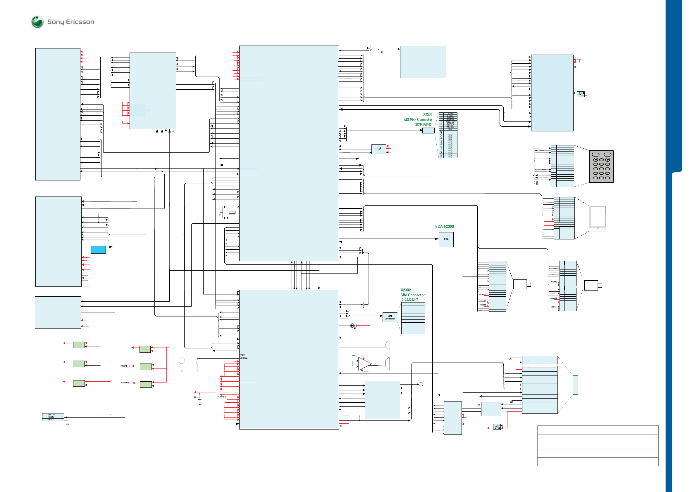
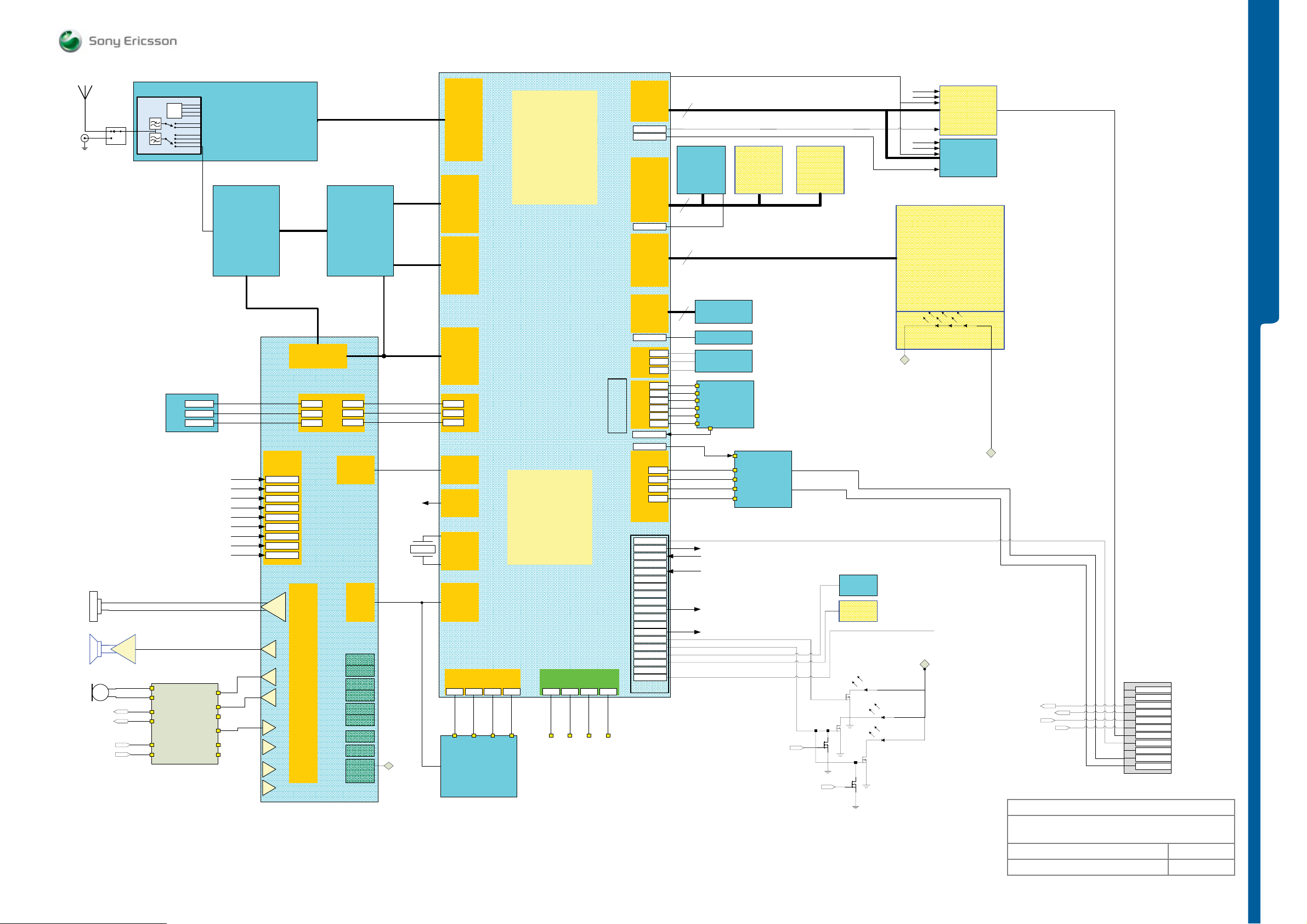
FUNCTION OVERVIEW
32
654
Document Nr Revision
1202-3085 rev. 2
9 (121)
Page 10
RECIEVER
SPK
MIC
SP Power
Amplifier
SPL
SPR
MIC+
MIC-
ANTSW 0
ANTSW 1
ANTSW 2
Control
ANTSW 3
GSM 900 RX
GSM 900 TX
GSM 1800 RX
GSM 1900R X
GSM 1800/1900 TX
WCDMA
SIMCONRST
SIMCONCLK
SIM
SIMCONDAT
Tjatte3
RF TEMP
RF VLOOP
UMTS POWER CNT
WRFLOOP
OPTO_SENSE
VBACKUP
OPTO(LCD)_TEMP
AID_AD
RF UMTS
RAY
VAD
RF GSM
MARLIN
GPADC
GPA1
GPA2
GPA3
GPA4
GPA5
GPA6
GPA7
GPA12
GPA13
BEAR
LINE
AUXO1
AUXO2
MIC1
AUXI1
AUXI2
AUXI3
WANDA
DAC
SIM LS
SRST
SCLK
SDAT
LDO_A
LDO_B
LDO_D
LDO_E
LDO_F
LDO_G
LPGEG
BOOST
SIMRST
SIMCLK
SIMDAT
CODEC
VINCENNE2
I2C 0
PCM I/F
BUCK
FB+
I2C#1
VBOOST
FUNCT I ON OVERVIEW
system
GSM Sub
ARM9EJ-S
208MHz
Inter
System
Interface
Serial Link
High Speed
Interface
DAC / ADC
MARIKA
SIMRST_
N
SIMCLK
SIMDAT
SIM I/F
#0
I2C
#1
I2C
DSP
Sub System
RTC
PCM I/F
UART3
GPIO20 GPIO21 GPIO22 GPIO23
BTTX
BTRX
BTCTS
BTRTS
SPI
GPIO24 GPIO25 GPIO26 GPIO27
SPIDI
SPIDO
SPIRDY
SPICLK
BT 2.0
Data and Signals
CIRES_N
GPIO46
GPIO47
8bit
512Mbit
NOR
Burst
EMIF CID
GPIO40
16bit
I/F
MEMDPD
8bit
DISPLAY
5×4
IRRXD
IRTXD
IRSD
MSSDIO0
MSSDIO1
MSSDIO2
MSSDIO3
MSSCLK
MSBS
MSDETECT
EDB_EN
DTMS
DFMS
USBRCV
USBBALID
KEY Matrix
MS Micro
KEY
PAD
GPIO41
GPIO44
GPIO45
GPIO46
IrDAMS I/F
MSSDIO0
MSSDIO1
MSSDIO2
MSSDIO3
MSSCLK
(UART6)
MSBS
GPIO34
GPIO42
GPIO00
GPIO01
GPIO02
GPIO03
UART0/USB
GPIO04
GPIO05
GPIO06
GPIO07
GPIO10 BTCLKREQ
GPIO11
GPIO12
GPIO13
GPIO14
GPIO15 AMPCTRL
GPIO16
GPIO17
GPIO30 DCIO_ON
GPIO31
GPIO32
GPIO33
GPIO35
GPIO36
GPIO37
CTMS
OPTOSENSESEL
PWM0 KBDIM
PWM1 NAVDIM
VBT_EN
CAM_27_EN
LCD_BL_ON
CFMS_AID
HS_USB_INT
PTT
IrDA
128Mbit
SDRAM
104MHz
Full USB
Transceiver
ISP1110
DISABLE_STAR
512Mbit
NAND
RAM
DISABLE_UNLOCK
VBT
REG
Camera
REG(2.7)
*
UNLOCK
I2CCLK1
I2CDAT1
VGA_PRESET
MPX1_OFF
I2CCLK1
I2CDAT1
RESET
VGA_OFF
LCD Back light
VBOOST
FB+
VBOOST
3.2M
CAM
VGA
CAM
Main LCD
VBOOST
STROBE
Made for
MIC+
SEMC Electrical Repair Manual
K800 - K810
FUNCTION OVERVIEW
1
VBUS
2
SPREF
3
Mic+/AUXinL
4
Mic-/AUXinR
MIC-
SPL
SPR
5
6
7
8
9
10
11
SPL
SPR
B
VIDEO/STROBE
AID/ACB/VPP
GND
D+/DTMS
D-/DFMS
Document Nr Revision
1202-3085 rev. 2
10 (121)
Page 11
FUNCT I ON OVERVIEW
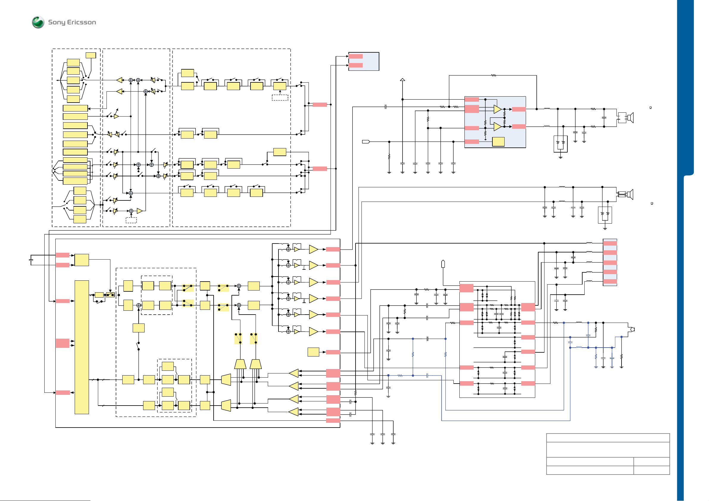
Acoustics
SEMC Electrical Repair Manual
K800 - K810
47nF
Audio Codec Audio Mixer
Silence
( PCM = 0 )
FR Speech
Encoder
HR Speech
Encoder
AMR Speech
Encoder
EFR Speech
Encoder
Transparent
PCM
Dictation FunctionallyRecord
Dictation Functionally Playback
AMR Speech Encoder
AMR-WB Encoder
ASR Algorithms
Tone Generator
MIDI or WAV
AMR Decoder
AMR-WB Decoder
E-AAC/AAC+/AAC,
MP3, WMA,
RealAudio/Video
DEC3
DEC4
PCMI
PCMSYN
PCMCLK
FR Speech
Decoder
HR Speech
Decoder
AMR Speech
Decoder
EFR Speech
Deccoder
C0a
Analog
PLL
C1a
C9abdfgh
CA a-h
DECODER
PCM 8/16/44/48
TWO CH.
PCM-IF
32
FIFO
C9abc
PCM8/16always
bypassFIFO
Selectable for
PCM44/48
0dB
0dB
DIGITAL FILTER
TxGC: 0dB
32 16
ENCODER
PCM 8/16
TWO CH.
PCMO
16
Vincenne2
ROP1013066/4
From Voice
C0g
C4abcd
VOL2
C4efgh
VOL1
C5ab
TX-GC
Call Tx
0dB
Codec power up
RX-FILTER
C9ab
RX2
HPF
RX1
HPF
C8efg
SIDE
TONE
C8h
TxPGA1: 0dB
C2fgh
TX-
PGA1
TxPGA2: 0dB
C2bcd
TX-
PGA2
RX2
LPF
RX1
LPF
TX-FILTER
C9ab
Audio Processing
PCM_A
PCM_B
Hard Limiter
Tx
DRC Tx CTM
Acoustic
Compensation
Noize
Reduction
Echo
Canceller
Loud Speaker signal
from Voice Call Rx
PCMDATB
Bluetooth Module
STLC2500B
RYT123922/1
470nF
VBATI
Vp(B3)
470Ω2.2kΩ
INM(A1)
INP(A3)
470Ω
0Ω
33pF
(NM)
VAD(B1)
CCO(B2)
MICPint(A1)
MICNint(A2)
INTMICint
SPLint(A3)
SPRint(A4)
Tjatte3
ROP1013074
BYPASS(C1)
SHUDOWN
(C3)
AUDIO_PA NCP2890
RYT101947/2
(B5)
Dynamic
Range
Control
Acoustic
Compensation
AMPCTRL(Marika_GPIO15)
SBC encoder
100kΩ
C5defgh
C6a-h
Dtnamic Range
Control
ADD2
CFc
ADD1
CEc
MUX2
MIC1/AUXI3
overrideAUXI1/AUXI
2inTX1/2MUX
Whining noize
C3bcd
RX-
PGA2
C3fgh
RX-
PGA1
CEcCFc
CEfgCFfg
MUX1
Filiter
CDef
CDab
CDgh
CDcd
CCef
C7be
CCab
C7d
CCgh
C7be
CCcd
CBef
C7b
CBab
CBgh
C7b
CBcd
C5cde
MIC 1
C5fgh
AUXI 1
C6fgh
AUXI 2
C6cde
AUXI 3
CTM
CFd
CEd
C6ab
TX1
MUX
TX2
MUX
LINEP
CDgh
LINEN
VMID
BEARP
C7d
CCgh
BEARN
VMID
AUXO1
CBcdgh
AUXO2
PCMDATA
Cdabef
D0a
C7fg
Ccabef
D0c
C7fg
CCcdgh
D0d
C7h
Cbabef
D0gh
C7h
D0ef
C0b
C1b
CCO CCO
LINEP
LINEN
BEARP
BEARN
AUXO1
AUXO2
MIC1P
MIC1N
AUXI1P
AUXI1N
AUXI2P
AUXI2N
AUXI3P
AUXI3N
DEC0
0Ω
100nF
100nF
33pF33pF
33pF
33pF
33pF33pF
0Ω(NM)
10uF
10uF
15kΩ
22pF(NM)
0Ω(NM)
↓
15kΩ
180Ω
100nF
100nF
100nF
100nF
220nF220nF33pF
Vincenne2_GPA5
33pF
1uF
(NM)
0Ω
(NM)
Acoustic
Compensation
Acoustic
Compensation
Acoustic
Compensation
C9ab
C9ab
TX1
HPF1
C1f
TX1
TX1
LPF
HPF3
TX2
HPF1
C1e
TX2
TX2
LPF
HPF3
Equalizer
Equalizer
DRC Voice
Call Rx
C0c
DAC2
C0d
DAC1
C0f
ADC1
C0e
ADC2
300k
300k
10kΩ
-
+
-
+
SHUTDOWN
CONTROL
50
50 50
50p 50p
1450 1450
20p
50
50
OUTA(A2)
R1
20k
R2
20k
OUTB(C2)
FB 1GHz
FB 1GHz
EMI FILTER
RKZ223914/1
33pF
(NM)
FB 1GHz
(0Ω)
FB 1GHz
(0Ω)
33pF
(NM)
33pF
(NM)
33pF
(NM)
33pF
(NM)
33pF 33pF
EMI FILTER
RKZ223914/1
(NM)
100MHz
100MHz
33pF
100MHz
(NM)
100MHz
100MHz
33pF
(NM)
FB
FB
FB
FB
FB
0Ω
0Ω
33pF
(NM)
SPREF(2pin)
Mic+/AUXinL
(3pin)
Mic+/AUXinR
(4pin)
SPL(5pin)
SPR(6pin)
Loudspeaker(8
Pogo-PIN
SXA1095652
Receiver(32 )
RLE90824
)
FUNCTION OVERVIEW
SYSTEM_CN
47k
1.1k
50
MICP(D2)
MICN(D3)
INTMIC(B5)
V_MIC(A5)
SP_ref(D1)
200p
SPL(D4)
200p
SPR(D5)
200p
0Ω
220pF
(NM)
220pF
(NM)
FB 1GH
(0Ω)
33nF
NM
1uF
NM
FB 1GH
(0Ω)
NM
1kΩ
1kΩ
33pF
(NM)
33pF
(NM)
0Ω
1_OUT
2_GND
MIC
RLC509429
Made for
Document Nr Revision
1202-3085 rev. 2
11 (121)
Page 12
FUNCT I ON OVERVIEW
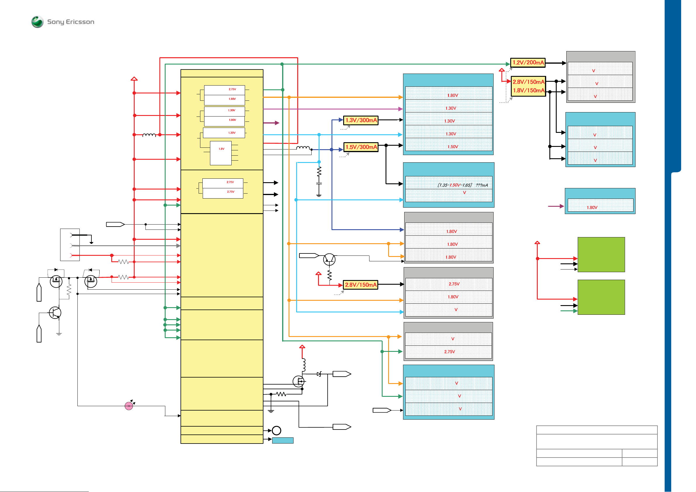
Power D istribution
SEMC Electrical Repair Manual
K800 - K810
DCIODCIO_ON
BAT CN
X2200
-
+
100kΩ
DCIO_INT
VBATI
VBUS
25mΩ
100mΩ
ChargeLED
Ferrite Beads
120Ω/2A
ERICSSON AB2010 Vincenne2
BASEBAND REGULATORS
LDO_D 2.70- -2.85
VBATB
VBATF
30-200mA max
LDO_E 1.75- -1.90
-170-200mA max
LDO_F 1.235- -1.360
30mA max
LDO_G 1.70- -1.90
30-200mA max
LPREG 1.265- -1.365
VBATC
BUCK
1.72- -1.9
400mA max
MOD1
RADIO
LDO_A 2. 70- -2.85
VBATA
VDDBUF
50-125mA max
LDO_B 2.70- -2.85
50-125mA max
VDDPA
BATTERY MANAGEMENT
VBUS
USBMOD
VBATD
BDATA
FGSENSEFGSENSE+
CHSENSECHSENSE+
CHREG
VDCIO
ANALOG BLOCK SUPPLY
VDDADC
AUDIO BLOCK SUPPLY
DIGVSS
DIGVDD
VDDCODEC
VDDBEAR
VDDIO_18
REF
VDDIO
SUB
TEST
VREF
IREF
LED1
Boost
LED
SWBOOST
LED2
Vibrator
Services
VDDD
VDDE
VDDF
VDDG
VDDLP
VDDBUCK
SWBUCK
VBUCK
VSSBUCK
VDDA
VDDB
EXTLDO
PAREG
ISENSE+
ISENSE-
FB+
VBOOST
VIBR
SIMVCC
VMSPICO
VccA
VccB
XTLDO
VAPC
Vib
SIM
VBATI
22uH
150mΩ
VRTC13
22uH
4.7kΩ
Backup
cap
VPP
VBATI
VDDF13
MAX1976AEETA-130
VCORE18
MAX1976AEETA-150
VCORE18
VCORE18
1kΩ
EN
VBT_EN
Key Backlight LED
LED+
LCD Backlight LED
LED-
VDDE18
/EN
/EN
R1115Z281B
VDDE18
VDIG
VCORE15
VBUS
VCORE13
VBT27
VBATI
DB2021 MARIKA
VDDEE [1.71-
VDDA [1.235-
CORE (ARM,DSP,RAM,GSM,UMA,TCM)
VDDC [1.235-
VDDRTC [1.235-
I/O WL (DAC ,HSSL ,ISI)
VDDEWL [1.35-
I/O E
-1.89] TBDmA
Analog cells / PLL
-1.365] TBDmA
-1.365] TBDmA
RTC
-1.365] TBDmA
-1.65] TBDmA
WANDA
WANDA VDD (DIGITAL)
VDD_1-22
VDDCLK32 [1.265-1.30 -1.65] ??
TBDmA
NOR + LPSDRAM
D-VCC [1.70-
F-VCC [1.70-
VCCQ [1.70-
SD-RAM VCC
-1.90] 130mA
NOR-Flash VCC
-2.00] 50mA
I/O VCC
-2.00] ???mA
Bluetooth STLC2500C
VDD_HV_A,D [XXX- -XXX] TBDmA
VDD_IO_A [1.65- -2.85] TBDmA
VDD_IO_B [1.35-1.30 -2.85] TBDmA
LCD
VCCIO [1.70-1.80 -1.90] TBDmA
VCC [XXX- -XXX] TBDmA
USB Transceiver (ISP1110)
VCC_IO [1.65-1.8 -2.85] 2mA
VCC_UART [2.7-2.8 -4.5] 8mA
VCC_5V0 [4.0-5.0 -5.5] 8mA
EN
CAM_27_EN
TPS79912YZU
R5323Z022B
EN
VMSPICO
VBATI
VccB
XTLDO
VccA
VDIG
Made for
[1.10-1.20
DVDD_Core
AVDD Analog
[2.45-2.70
[1.70-1.80
VGA Camera
VDD_Analog
[2.45-2.70
[1.70-1.80
[1.70-1.80
MS pico
[1.70-
RAY MODULE
VBATI
VccB
XTLDO
MARLIN MODULE
VBATI
VRAD
VDIG
Camera
-1.30] 50mA max
-2.80] TBDmA
VDD_IO
-3.30] TBDmA
FUNCTION OVERVIEW
-2.80] TBDmA
VDD_Core
-1.90] TBDmA
VDD_IO
-3.30] TBDmA
VCC
-1.95] TBDmA
(UMTS)
(GSM)
Document Nr Revision
1202-3085 rev. 2
12 (121)
Page 13
FUNCT I ON OVERVIEW
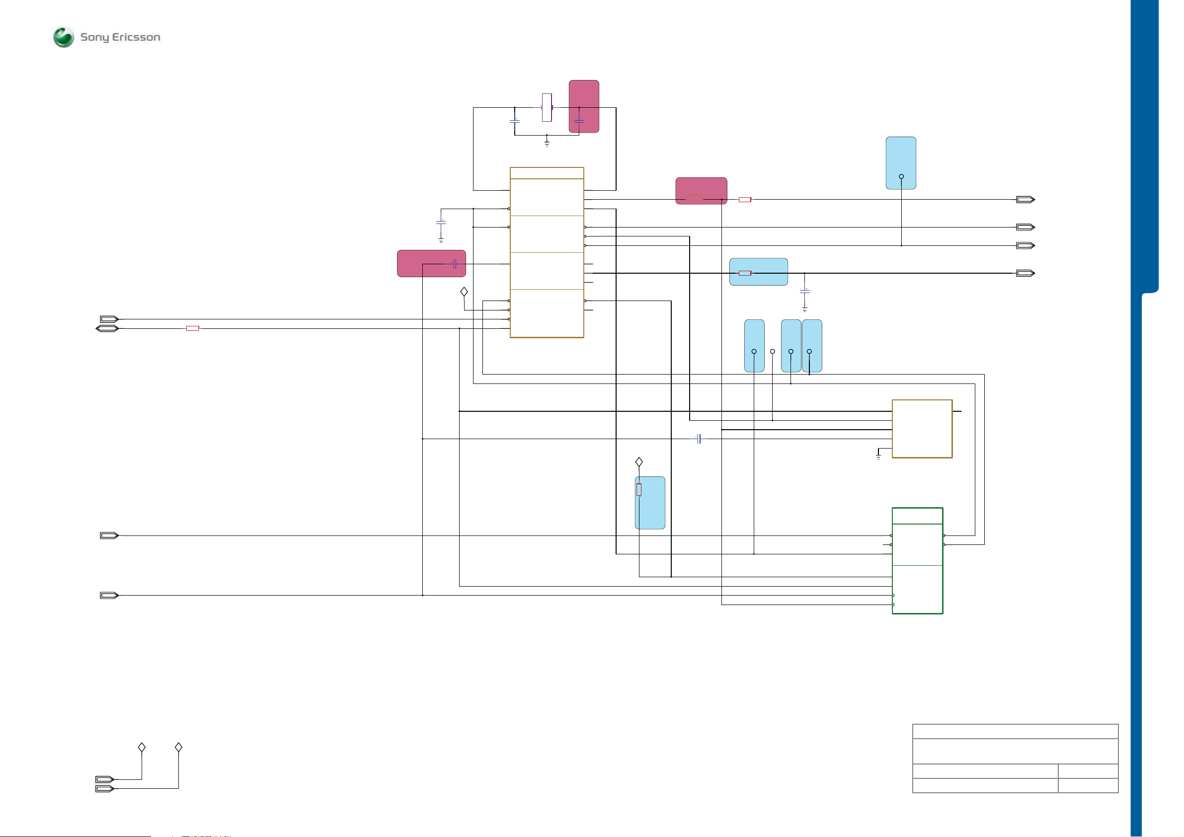
BTCTS
BTRX
PCMDATB
PCMDATA
BTCLKREQ
Baseband Top - Radio To p - Bl uetooth - FM RadioBaseband Top - Radio To p - Bl uetooth - FM Radio
VDDE18
VBT27
VRTC13
MP 138
Page 47
SEMC Electrical Repair Manual
K800 - K810
BTCLKREQ
PCMDATA
PCMDATB
BTRX
BTCTS
RXQB
RXQA
RXIA
RXIB
RTEMP
VLOOP
WRFLOOP
IDATA
QDATA
DCLK
DIRMODCLK
FMINT
FMR
FML
BTCLKREQ
PCMDATA
PCMDATB
BTRX
BTCTS
RXQB
RXQA
RXIA
RXIB
MCLK
RTEMP
VLOOP
WRFLOOP
IDATA
QDATA
DCLK
DIRMODCLK
FMINT
FMR
FML
Baseband
Baseband
Page 19
VBATI
VDDE18
VDIG
VBT27
VFM27
VRTC13
BTRESn
PCMSYN
PCMCLK
BTTX
BTRTS
RTCCLK
WPABIAS
VCXOCONT
WSTR
WDAT
WCLK
TXQB
TXQA
TXIA
TXIB
CLKREQ
RADSTR
RADDAT
RADCLK
TXON
MODA
MODB
MODC
MODD
ANTSW0
ANTSW1
ANTSW2
ANTSW3
I2CDAT1
I2CCLK1
FM_ANTENNA
VBATI
VDIG VBT27 VFM27 VRTC13
VDDE18
BTRESn
PCMSYN
PCMCLK
BTTX
BTRTS
RTCCLK
WPABIAS
VCXOCONT
WSTR
WDAT
WCLK
TXQB
TXQA
TXIA
TXIB
CLKREQ
RADSTR
RADDAT
RADCLK
TXON
MODA
MODB
MODC
MODD
ANTSW0
ANTSW1
ANTSW2
ANTSW3
DIRMODCLK
DCLK
QDATA
IDATA
WRFLOOP
VLOOP
RTEMP
RXIB
RXIA
RXQA
RXQB
RTCCLK
I2CDAT1
I2CCLK1
FM_ANTENNA
FML
FMR
FMINT
VFM27VDDE18
VFM27
VDDE18
RTCCLK
I2CDAT1
I2CCLK1
FM_ANTENNA
FM RadioFM Radio
Page 42
FMINT
FMR
FML
VBT27
VDDE18
VRTC13
MCLK_BT
BTRESn
PCMSYN
PCMCLK
BTTX
BTRTS
RTCCLK
Bluetooth
Bluetooth
VBATIVDIG
X1001
ANT
VBATI
VDIG
WPABIAS
VCXOCONT
WSTR
WDAT
WCLK
TXQB
TXQA
TXIA
TXIB
CLKREQ
RADSTR
RADDAT
RADCLK
TXON
MODA
MODB
MODC
MODD
ANTSW0
ANTSW1
ANTSW2
ANTSW3
Radio
Radio
ANT
RXQB
RXQA
RXIA
RXIB
MCLK
RTEMP
VLOOP
WRFLOOP
IDATA
QDATA
DCLK
DIRMODCLK
MCLK_BT
1
X1002
1
RXQB
RXQA
RXIA
RXIB
RTEMP
VLOOP
WRFLOOP
IDATA
QDATA
DCLK
DIRMODCLK
RPT79951
RPT79951
MCLK_BT
Page 18
BTANT
BTCLKREQ
PCMDATA
PCMDATB
BTRX
BTCTS
CLKREQ
BTANT
Front upper ESD connection.
Front lower ESD connection.
TP1000
TP1001
X1400
1
X1401
1
<NM>
CONNECTORPAD
<NM>
CONNECTORPAD
FUNCTION OVERVIEW
Page 14
E1002
Clamp
1
GND
Will be connected
to GND in PCB
SHIELDCAN_CYNDI_BT
SXA1096043
R1A
E1003
Clamp
1
GND
Will be connected
to GND in PCB
SHIELDCAN_WILMA_CAMERA
SXA1096981
R1A
E1000
Clamp
1
GND
Will be connected
to GND in PCB
SHIELDCAN_CYNDI_WANDA
SXA1095997
R1A
E1001
Clamp
1
GND
Will be connected
to GND in PCB
SHIELDCAN_MARIKA-WILMA
SXA1096372
R1A
Made for
Baseband Top - Radio Top Bluetooth - FM Radio
Document Nr Revision
1911 - ROA 128 1534/2 A
1202-3085 rev. 2
13 (121)
Page 14
FUNCT I ON OVERVIEW
Radio - Top
SEMC Electrical Repair Manual
K800 - K810
TXON
ANTSW3
ANTSW2
ANTSW1
ANTSW0
MODA
MODB
MODC
MODD
RADSTR
RADDAT
RADCLK
VccA
VDIG
VBATI
VAPC
XOOA
XOOB
TXON
ANTSW3
ANTSW2
ANTSW1
ANTSW0
MODA
MODB
MODC
MODD
RADSTR
RADDAT
RADCLK
CLKREQ
VBATI
VDIG
VccA
DIRMODCLK
WCDMA_ANT
R04_GSM
Page 17
VLOOP
DCLK
QDATA
IDATA
GSM_ANT
C1000
22pF
MP 118
Page 47
L1000
68nH
NM
X1000
31
IO ANT
4
2
C04000390-O51
RPT79953
GND
6
5
R1000
0ohms
R1002
0ohms
<NM>
DIRMODCLK
VLOOP
DCLK
QDATA
IDATA
MP 115
Page 47
ANT
X1001
FUNCTION OVERVIEW
VBATI
VDIG
VCXOCONT
WPABIAS
WCLK
WDAT
WSTR
CLKREQ
TXQB
TXQA
TXIB
TXIA
VBATI
VDIG
VDIG
VBATI
VBATI
VDIG
R02_PowerSupply
Page 15
VAPC
XTLDO
VccA
VccB
VccA
VccB
VDIG
VccB
VBATI
VCXOCONT
XTLDO
WPABIAS
WCLK
WDAT
WSTR
CLKREQ
TXQB
TXQA
TXIB
TXIA
VBATI
VccB
VDIG
Page 16
R03_UMTS
XOOA
XOOB
WCDMA_ANT
WRFLOOP
RTEMP
MCLK
RXQB
RXQA
RXIB
RXIA
MCLK_BT
WRFLOOP
RTEMP
MCLK
RXQB
RXQA
RXIB
RXIA
MCLK_BT
Made for
RADIO TOP
Document Nr Revision
1/1911 - ROA 128 1534/2 A
1202-3085 rev. 2
14 (121)
Page 15
PA Control
FUNCT I ON OVERVIEW
Radio - Power Supply
SEMC Electrical Repair Manual
K800 - K810
VDIG
Power Supply
VBATI
C1100
10nF
N2000
ERICSSON AB 2012
C12
VDDBUF
G12
VDDPA
ERICSSON_AB2012
ROP1013066/6
UMTS ACCESS
PACONTROL
R1A
LEADFREE
PASENSE+
PASENSE-
PAREG
IOUT
FF_IN
EXPOUT
VSSPA
FUNCTION OVERVIEW
E12
E11
MP 36
C1102
470pF
Page 46
R1100
820ohms
D11
D12
F10
G10
E10
C1101
470pF
VAPC
VBATI
VDIG
VBATI VDIG
VBATI
C1103
4.7uF
N2000
ERICSSON AB 2012
ERICSSON_AB2012
ROP1013066/6
LEADFREE
POWER
RADIO
LDO_A
LDO_B
R1A
VDDAVBATA
VDDB
EXTLDO
VSSA
MP 35
Page 46
C1106
10uF
B12A12
A11
C11
H10
MP 34
Page 46
C1107
10uF
VccA
VccB
XTLDO
Made for
RADIO - Power Supply
Document Nr Revision
1/1911 - ROA 128 1534/2 A
1202-3085 rev. 2
15 (121)
Page 16
FUNCT I ON OVERVIEW
A1200
RAY_MODULE_IF
WCDMA_ANT
TXIA RXIA
TXIB
TXQA
TXQB
CLKREQ
WSTR
WDAT
WCLK
WPABIAS
XTLDO
VCXOCONT
VBATI
VccB
58
TXIA
59
TXIB
60
TXQA
61
TXQB
12
CLKREQ
52
WSTR
53
WDAT
54
WCLK
WPABIAS
47
XTLDO
66
VCXOCONT
35
VBATI
36
VBATI
37
VBATI
38
VBATI
39
VBATI
9
VccB
1
VccB_mix
RAY_MODULE
ROA1281112
Radio - UMTS
WCDMA_SENSE
RXIA
RXIB
RXQA
RXQB
XOOA
XOOB
MCLK
RTEMP
WRFLOOP
WON
POWER/GND
GND pins
are hidden
R1A
WCDMA_ANT
3020
69
68
71
70
5
4
63
MCKL_1
45
1532
56
GND
C1302
10nF
<N.M>
C1301
100pF
<N.M>
<N.M>
L1300
1uH
MP 99
Page 47
ST1300
12
GND
C1300
100nF
MCLK_BT
R1301
10ohms
VDIG
C
B
V1300
BFR193L3
RYN121933/2
E
RXIB
RXQA
RXQB
XOOA
XOOB
RTEMP
WRFLOOP
MCLK_BT
SEMC Electrical Repair Manual
K800 - K810
FUNCTION OVERVIEW
VBATI
VccB
VDIG
VBATI VccB
VDIG
1
G
V1301
2
LEADFREE
SI1012R_LEADFREE
RYN123911/2
GND
MCLK
R1304
3.9Kohms
3
DS
MCLK
Made for
RADIO - UMTS
Document Nr Revision
1/1911 - ROA 128 1534/2 A
1202-3085 rev. 2
16 (121)
Page 17
FUNCT I ON OVERVIEW
Radio - GSM
SEMC Electrical Repair Manual
K800 - K810
XOOA
XOOB
TXON
ANTSW3
ANTSW2
ANTSW1
ANTSW0
MODA
MODB
MODC
MODD
RADSTR
RADDAT
RADCLK
CLKREQ
VAPC
A1300
20
XOOA
22
XOOB
7
TXON
3
ANTSW3
4
ANTSW2
5
ANTSW1
6
ANTSW0
24
MODA
25
MODB
26
MODC
27
MODD
17
RADSTR
18
RADDAT
19
RADCLK
30
CLKREQ
53
VAPC
MARLIN_MODULE
ROA1281640
MARLIN_IO
WCDMA_ANT
R1B
ANT
TESTOUT
IDATA
QDATA
DCLK
VLOOP
48
23
36
34
35
15
46
GSM_ANT
DIRMODCLK
IDATA
QDATA
DCLK
VLOOP
WCDMA_ANT
FUNCTION OVERVIEW
VBATI
VDIG
VccA
A1300
VDIG
VccAVBATI VDIG
VccA
VBATI
MARLIN_POWER
39
VDIG
10
VRAD
1
VBATTI
2
VBATTI
62
VBATTI
63
VBATTI
130
VBATTI
MARLIN_MODULE
ROA1281640
R1B
Made for
RADIO - GSM
Document Nr Revision
1/1911 - ROA 128 1534/2 A
1202-3085 rev. 2
17 (121)
Page 18
BTRESn
MCLK_BT
RTCCLK
BTRTS
PCMCLK
PCMSYN
PCMDATB
PCMDATA
BTTX
C1408 10nF
MP 133
Page 47
12
12
ST1400
PCMDATB
PCMDATA
ST1401
VDDE18
D1400
BT-FUNCTIONAL
D3
D6
G3
C5
D1
C2
D2
E1
B3
C3
B1
C1
D5
E6
G6
E2
F1
F2
E5
CLOCK AND RESET
RESETn
REF_CLK_IN
LP_CLK
SW INITIATED LOW POWER MODE
BT_WAKEUP
UART INTERFACE
UART_RXD/SPI_DI
UART_CTS/SPI_CLK
PCM_CLK
PCM_SYNC
PCM_A
PCM_B
JTAG_NTRST/GPIO_16
JTAG_TCK/GPIO_8
JTAG_TDI/GPIO_9
JTAG_TMS/GPIO_10
GEN_PURPOSE/GPIO_0
CLK_REQ_IN_1
CLK_REQ_IN_2
CONFIG_1
CONFIG_2
CONFIG_3
AF_PRG
PCM INTERFACE
CONFIGURATION
PINS
LEAVE UNCONNECTED
FUNCT I ON OVERVIEW
HOST_WAKEUP/SPI_INT
UART_TXD/SPI_DO
UART_RTS/SPI_CSN
JTAG/GPIO
JTAG_TDO/GPIO_11
CLK_REQ_OUT_1
CLK_REQ_OUT_2
TEST-PIN
F7
F6F5
F4G4
B2
C4
G7
RF
RFP
A3
A4
RFN
ST1402
12
Z1400
4
5
Freq
BAL
BAL_DC-FEED
BAL
DEA212450BT-7043D1
RTN202932/4
12
UNBAL
ST1403
GNDGND
Radio - Bluetooth
R1404 10K ohms
100Kohms
R1405
R1406
0ohms
<NM>
L4122
4.7nH
C4152
<NM>
1.2pF
D1400
VBT27
A7
VDD_HV_A
G1
VDD_HV_D
VDDE18
G5
F3
E7
VDD_IO_A
VDD_IO_B
VDD_CLD
1
2
63
VRTC13
CLKREQ
BTCLKREQ
BT-SUPPLY
POWER SUPPLY
2.75V
1V65 to 2V85
IOs SUPPLY
1V17 to 2V85
IOs SUPPLY
1V65 to 2V85
SYSTEM CLOCK
SUPPLY
BTANT
DIGITAL GROUND
VSS_DIG
VSS_DIG
E3
E4
SEMC Electrical Repair Manual
K800 - K810
CLKREQ
BTCLKREQ
BTRX
BTCTS
BTANT
FUNCTION OVERVIEW
VBT27
VDDE18
VRTC13
VBT27 VDDE18 VRTC13
RYT123923/2
STLC2500C4
C1403
220nF
C1402
220nF
C1401
220nF
C1400
220nF
C1409
100nF
C1405
220nF
C1411
220nF
C1407
1uF
C1404
220nF
B7
C7
D7
A1
B5
A6
RYT123923/2
STLC2500C4
INTERNAL SUPPLY
DECOUPLING
VDD_DSM
VDD_N
VDD_CL
VDD_RF
TEST PINS
TOUT_IN_QP
TOUT_IP_QN
ANALOG GROUND
VSS_ANA
VSS_ANA
VSS_ANA
RF GROUND
VSS_RF
VSS_RF
OUTPUT
REGULATOR
FOR CORE LOGIC
VDD_D
B4
B6
C6
A2
A5
G2
C1406
220nF
Made for
RADIO - Bluetooth
Document Nr Revision
1/1911 - ROA 128 1534/2 A
1202-3085 rev. 2
18 (121)
Page 19
FUNCT I ON OVERVIEW
Baseband - Logic Top
SEMC Electrical Repair Manual
K800 - K810
RXQB
RXQA
RXIB
RXIA
IDATA
QDATA
DCLK
DIRMODCLK
FMR
FML
VLOOP
RTEMP
WRFLOOP
BTCLKREQ
BTRX
BTCTS
FMINT
VBATIVDIGVDDE18VMSPICOVBACKUP
VLOOP
RTEMP
WRFLOOP
BTCLKREQ
BTRX
BTCTS
FMINT
Pages 28-33
VBATI
VDIG
VDDE18
VMSPICO
FOCUSLED_ON
VBACKUP
STROBE_ENABLE
VLOOP
RTEMP
WRFLOOP
BTCLKREQ
BTRX
BTCTS
FMINT
MEMRESn
VAD
FLASH_STROBE
OPTOTEMP
CAMIRQ
SPL
SPR
MIDREF
LIDSENSE
CHARGE_RDY
Operation & Services
Operation & Services
CHARGE_ON
LKEYBRGT
UKEYBRGT
AMPCTRL
MICN/AUXinR
MICP/AUXinL
CAMDIR
I2CDAT1
I2CCLK1
FM_ANTENNA
BTTX
BTRTS
WPABIAS
VCXOCONT
VBUS
DCIO
DCIO_ON
VBT_EN
CAM_27_EN
CAM_12_EN
FM_EN
SERVICEn
VPP
FMR
FML
FOCUSLED_ON
CHARGE_ON
LKEYBRGT
UKEYBRGT
AMPCTRL
STROBE_ENABLE
MICN/AUXinR
MICP/AUXinL
CAMDIR
I2CDAT1
I2CCLK1
FM_ANTENNA
BTTX
BTRTS
WPABIAS
VCXOCONT
CAMSYSCLK
RXQB
RXQA
RXIB
RXIA
IDATA
QDATA
DCLK
DIRMODCLK
V_VGAANA
V_VGADIG
VBATI
VDIG
VCAM27
VCAMAF
VCAM12
VDDE18
VCAMIO
VCAMSD
DCIOint
Pages 37-42
V_VGAANA
V_VGADIG
VBATI
VDIG
VCAM27
VCAMAF
VCAM12
VDDE18
VCAMIO
VCAMSD
FMR
FML
FOCUSLED_ON
CHARGE_ON
LKEYBRGT
UKEYBRGT
AMPCTRL
STROBE_ENABLE
FLASH_STROBE
MICN/AUXinR
MICP/AUXinL
CAMDIR
I2CDAT1
I2CCLK1
CAMSYSCLK
CHARGE_RDY
DCIOint
MMI
MMI
I2CDAT1
I2CCLK1
FM_ANTENNA
BTTX
BTRTS
WPABIAS
VCXOCONT
ONSWA
CHARGE_RDY
LIDSENSE
MIDREF
SPR
SPL
CAMIRQ
OPTOTEMP
FLASH_STROBE
VAD
PCMDATA
PCMDATB
PCMSYN
PCMCLK
VAD
OPTOTEMP
CAMIRQ
SPL
SPR
MIDREF
LIDSENSE
ONSWA
VCORE15
Pages 34-36
VDIGVDDE18
VDIG
VDDE18
VCORE15
RXQB
RXQA
RXIB
RXIA
IDATA
QDATA
DCLK
DIRMODCLK
UMTS Access
UMTS Access
WSTR
WDAT
WCLK
TXQB
TXQA
TXIA
TXIB
RADSTR
RADDAT
RADCLK
TXON
MODA
MODB
MODC
MODD
ANTSW0
ANTSW1
ANTSW2
ANTSW3
PCMDATA
PCMDATB
PCMSYN
PCMCLK
VDDE18
WSTR
WDAT
WCLK
TXQB
TXQA
TXIA
TXIB
RADSTR
RADDAT
RADCLK
TXON
MODA
MODB
MODC
MODD
ANTSW0
ANTSW1
ANTSW2
ANTSW3
VRTC13
VDIGVBT27VFM27
WSTR
WDAT
WCLK
TXQB
TXQA
TXIA
TXIB
RADSTR
RADDAT
RADCLK
TXON
MODA
MODB
MODC
MODD
ANTSW0
ANTSW1
ANTSW2
ANTSW3
PCMDATA
PCMDATB
PCMSYN
PCMCLK
I2CDAT1
I2CCLK1
FM_ANTENNA
BTTX
BTRTS
WPABIAS
VCXOCONT
VBATI
VBATI
VDIG
VRTC13
VBT27
VFM27
VDDE18
FUNCTION OVERVIEW
CLKREQ
MCLK
BTRESn
RTCCLK
BTRESn
RTCCLK
Pages 23-27
VBATI
VDIG
VBT27
VFM27
V_VGADIG
V_VGAANA
VCAMSD
VCAMIO
VBATI
VDIG
VBT27
VDDE18
VBACKUP
VCAM27
VCAMAF
VCAM12
VMSPICO
VFM27
DCIOint
VRTC13
VCORE15
Made for
BASEBAND - Logic TOP
Document Nr Revision
2/1911 - ROA 128 1534/2 A
1202-3085 rev. 2
19 (121)
V_VGADIG
V_VGAANA
VCAMSD
CAMDIR
VPP
VBUS
DCIO
DCIO_ON
VBT_EN
CAM_27_EN
CAM_12_EN
FM_EN
VCAMIO
VDDE18
VBACKUP
VCAM27
VCAMAF
VCAM12
VMSPICO
DCIOint
VRTC13
VCORE15
VDDE18VCORE15
Pages 20-22
VDDE18
VCORE15
CLKREQ
MCLK
SERVICEn
CAMSYSCLK
ONSWAn
System Control
System Control
MEMRESn
BTRESn
RTCCLK
ONSWA
SERVICEn
CAMSYSCLK
CAMDIR
VPP
VBUS
DCIO
DCIO_ON
VBT_EN
CAM_27_EN
CAM_12_EN
FM_EN
Page 20
VDDE18 VCORE15 VDDE18VCORE15
FUNCT I ON OVERVIEW
Page 21
Page 3Page 3
Baseband - System Co nt rol Top
SEMC Electrical Repair Manual
K800 - K810
FUNCTION OVERVIEW
VDDE18
VCORE15
CLKREQ
MCLK
SERVICEn
ONSWAn
CLKREQ
MCLK
SERVICEn
ONSWAn
VDDE18
VCORE15
CLKREQ
MCLK
SERVICEn
ONSWAn
Clocks & Resets
Clocks & Resets
Page 22
Page 4Page 4
RTCCLK
CAMSYSCLK
MEMRESn
BTRESn
RTCCLK
CAMSYSCLK
MEMRESn
BTRESn
RTCCLK
CAMSYSCLK
MEMRESn
BTRESn
Test
Test
Made for
BASEBAND - System Control Top
Document Nr Revision
2/1911 - ROA 128 1534/2 A
1202-3085 rev. 2
20 (121)
Page 21
FUNCT I ON OVERVIEW
Baseband - System Co nt rol Cloc ks an d Re set s
SEMC Electrical Repair Manual
K800 - K810
SERVICEn
CLKREQ
ONSWAn
MCLK
R2102
100ohms
SERVICEn
CLKREQ_1
PIC 54
Page 46
C2104
1nF
C2100
1nF
VDDE18
B2100
RTM501911/2
C2102
22pF
D2000
MARIKA_SYSTEM_CONTROL
RTCIN
R14
RTCBDIS_N
Y16
RESPOW_N
AA15
MCLK
J2
IRQ0_N
K4
IRQ1_N
J8
SERVICE_N
V19
CLKREQ
DB2021_MARIKA_SECURITY_EFUSE
ROP1013083/4 R2A
C2C1
32.768kHz
RTC
Resets
Clocks
Control
Page 46
RTCOUT
RTCCLK
RTCDCON
RESOUT0_N
RESOUT1_N
RESOUT2_N
SYSCLK0
SYSCLK1
SYSCLK2
PWRREQ0_N
PWRREQ1
PIC 53
C2103
22pF
R13
V21
T19
R18
U19
W17AA17
W15
W21
W20
MP 67
Page 46
SP2105
PIC 52
Page 46
ST2100
12
J7
J1
1nF
C2101
VCORE15
100Kohms
R2101
MP 55
Page 46
R2105 1 0Kohms
R2104 47ohms
MP 30
Page 46
SP2100
MP 60
Page 47
MP 31
Page 46
C2105
33pF
MP 50
Page 46
SP2103SP2102SP2101
RTCDCON
RTCCLK
MEMRESn
BTRESn
CAMSYSCLK
PWR_IRQ
PWRRST
CLKREQ_1
WANDARESn
RTCCLK_1
MCLK_WANDA
ONSWAnONSWAn
PWRREQn
CLKREQ_1
MCLKMCLK
RTCCLK_1
D2001
EMP_WANDA_SYSTEM_IF
T15
CLKRQ
N13
RESET
T16
CLK32
U13
MCLK
R15
HCLK
ROP1013044/4
N2000
ERICSSON AB 2010
SYSTEM CONTROL
POWER ON/RESET
C4
ONSWA
C5
ONSWB
A7
ONSWC
CONTROL
C10
SLEEP
K3
CLKREQ
K9
MCLK
M1
XTAL1
ERICSSON_AB2012
ROP1013066/6
LEADFREE
Leadfree
R1B
PWRRST
R1A
ID_BALL
IRQ
RTCCLK
MEMRESn
BTRESn
CAMSYSCLK
D4
B8
C1
FUNCTION OVERVIEW
VDDE18
VCORE15
VDDE18 VCORE15
Made for
BASEBAND - System Control
Clocks & Resets
Document Nr Revision
2/1911 - ROA 128 1534/2 A
1202-3085 rev. 2
21 (121)
Page 22
FUNCT I ON OVERVIEW
Baseband - System Co nt rol Test
SEMC Electrical Repair Manual
K800 - K810
SP2106
SP2107
SP2108
SP2109
MARIKA_TDI
MARIKA_TMS
MARIKA_TCK
MARIKA_TRSTn
D2000
MARIKA_TEST_AND_EMULATION
JTAG_IF
TDI
R19
TMS
V20
TCK
P18
TRST_N
ETM_IF
ETMPSTAT0
ETMPSTAT1
ETMPSTAT2
ETMTSYNC
DB2021_MARIKA_SECURITY_EFUSE
ROP1013083/4 R2A
TDO
RTCK
TEMU0_N
TEMU1_N
ETMTCLK
ETMTPKT0
ETMTPKT1
ETMTPKT2
ETMTPKT3
ETMTPKT4
ETMTPKT5
ETMTPKT6
ETMTPKT7
U20P14
T21
P19
T20
M15
M14
M20
K20
K19
H20
K15
D2001
EMP_WANDA_SWDEBUG
MARIKA_TDO
MARIKA_RTCK
MARIKA_TEMU0n
MARIKA_TEMU1n
L19
L18
L15
L20
L14
J20
SP2110
SP2111
SP2112
SP2113
UART_RX
DSP INTERRUPT
ROP1013044/4
D2001
EMP_WANDA_TEST_IF
JTAG_TDI
G15
JTAG_TMS
G16
JTAG_TRSTN
G17 E15
JTAG_TCK
ROP1013044/4
D2001
EMP_WANDA_MODE_SEL
C17
BOOTMODE0
B17
BOOTMODE1
E13
BOOTMODE2
C15
BOOTMODE3
D15
TESTMODE
E11
ANALOG_ENABLE
C11
APLL_BYPASS
A11
CS_BYPASS
ROP1013044/4
CPU_IACK
CPU_IRQ1
CPU_IRQ0
CPU_CLKOUT
R1A
JTAG_TDO
EMU0
EMU1
R1A
APLL_ATEST1
R1A
GPO0
GPO1
GPO2
GPO3
GPO4
GPO5
GPO6
GPO7
UART_TX
CPU_XF
U12
L17
K13
K15
K16
J15
J13
H15
H13
E12C13
N6
R5
N7
R6
M17
G13F16
F13
D2001
Wanda_External_MEM_IF
C2
EMIF_D0
C1
EMIF_D1
F5
EMIF_D2
E3
EMIF_D3
G5
EMIF_D4
E1
EMIF_D5
F2
EMIF_D6
F1
EMIF_D7
G3
EMIF_D8
G2
EMIF_D9
H5
EMIF_D10
H1
EMIF_D11
H2
EMIF_D12
J2
EMIF_D13
J3
EMIF_D14
J5
EMIF_D15
K3
EMIF_D16
K5
EMIF_D17
K1
EMIF_D18
L1
EMIF_D19
L3
EMIF_D20
M2
EMIF_D21
L5
EMIF_D22
N1
EMIF_D23
M3
EMIF_D24
M5
EMIF_D25
P2
EMIF_D26
P3
EMIF_D27
R2
EMIF_D28
T1
EMIF_D29
N5
EMIF_D30
U1
EMIF_D31
EXT_FRAME_STROBE
ROP1013044/4
EMIF_AWE
EMIF_ARE
EMIF_ARE_ADY
EMIF_A1
EMIF_A2
EMIF_A3
EMIF_A4
EMIF_A5
EMIF_A6
EMIF_A7
EMIF_A8
EMIF_A9
EMIF_A10
EMIF_A11
EMIF_A12
EMIF_A13
EMIF_A14
EMIF_A15
EMIF_A16
EMIF_A17
EMIF_A18
EMIF_A19
EMIF_A20
EMIF_A21
EMIF_A22
EMIF_A23
EXT_MEM_UBUS10
EXT_MEM_UBUS11
EXT_MEM_UBUS12
R1A
E10
A10
C10
N12
T14
R14
E17
U3
T3
U2
B9
C9
E9
C8
E8
A8
A7
C7
B6
E7
A5
C6
E6
B4
C4
B3
A2
A1
E5
B2
FUNCTION OVERVIEW
Made for
BASEBAND - System Control Test
Document Nr Revision
2/1911 - ROA 128 1534/2 A
1202-3085 rev. 2
22 (121)
Page 23
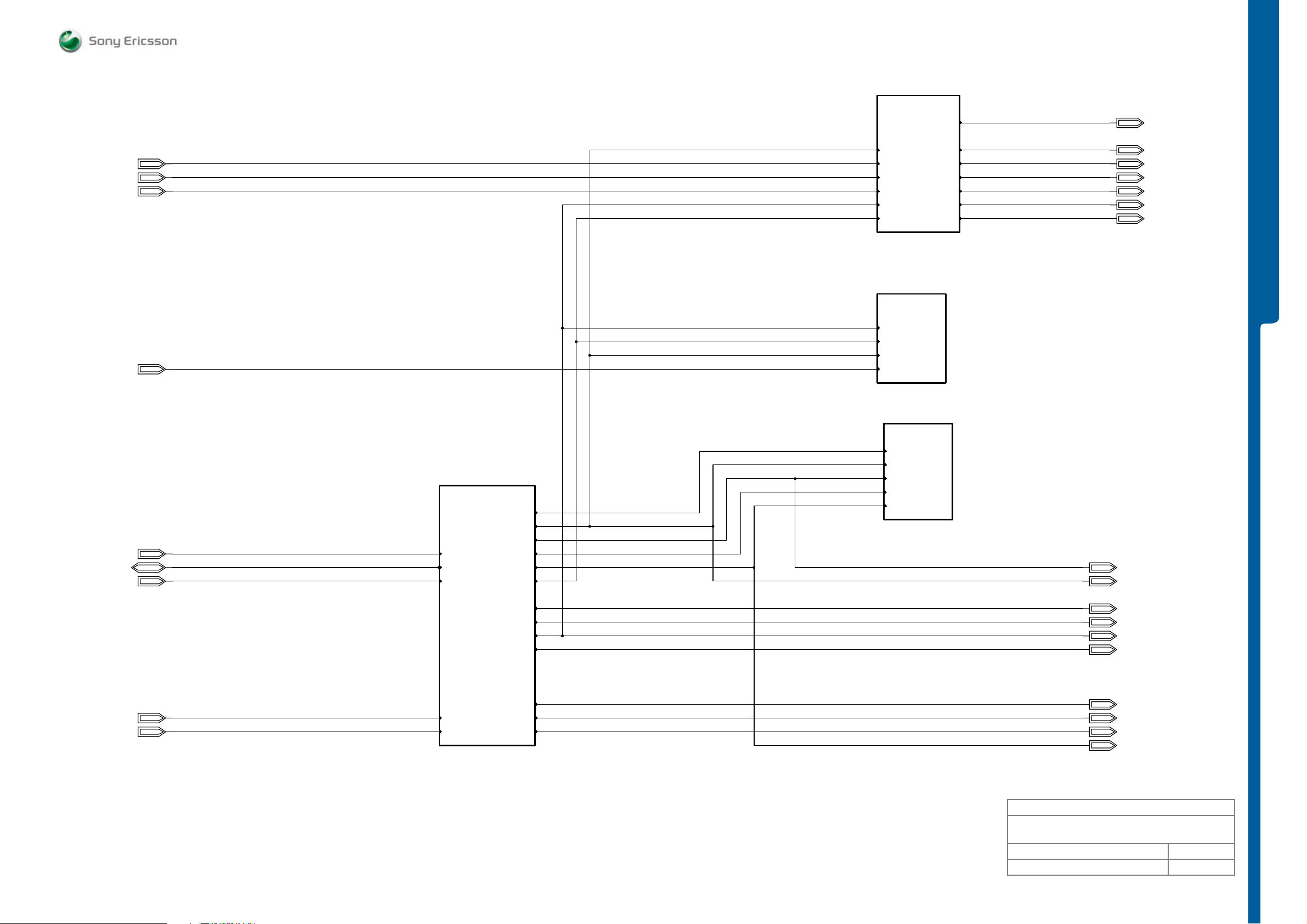
FUNCT I ON OVERVIEW
Baseband - Power Top
Page 25
V_VGADIG
V_VGADIG
SEMC Electrical Repair Manual
K800 - K810
V_VGADIG
VDDE18
CAMDIR
CAM_27_EN VCAM12
CAM_12_EN
CAMDIR
CAM_27_EN
CAM_12_EN
VDDE18
CAMDIR
CAM_27_EN
CAM_12_EN
VBATI
VCORE18
Camera Power
Camera Power
V_VGAANA
VCAM27
VCAM12
VCAMAF
VCAMIO
VCAMSD
V_VGAANA
VCAM27
VCAM12
VCAMAF
VCAMIO
VCAMSD
V_VGAANA
VCAM27
VCAMAF
VCAMIO
VCAMSD
Page 27
VPP
VBATI
VCORE18
VDDE18
VPP VPP
VBATI
VCORE18
VDDE18
VPP
Memories
Memories
Page 26
VBUS
DCIO
DCIO_ON
VBUS
DCIO
DCIO_ON
VBUS
DCIO
DCIO_ON
Page 24
VDDF13
VDDE18
VRTC13
VCORE13
VCORE15
VCORE18
VDDF13
VDDE18
VRTC13
VCORE13
VCORE15
VDDE18
VDDF13
VDDE18
VRTC13
VCORE13
VCORE15
Power Asics
Power Asics
VRTC13
VDDE18
FUNCTION OVERVIEW
VBT27
VBACKUP
VBATI
VDIG
VBT_EN
FM_EN DCIOint
VBT_EN
FM_EN
VBT_EN
FM_EN
Regulators & Charging
Regulators & Charging
VMSPICO
VFM27
DCIOint
VBT27
VBACKUP
VBATI
VDIG
VMSPICO
VFM27
DCIOint
VBT27
VBACKUP
VBATI
VDIG
VMSPICO
VCORE15
Made for
BASEBAND - Power Top
Document Nr Revision
2/1911 - ROA 128 1534/2 A
1202-3085 rev. 2
VFM27
23 (121)
Page 24
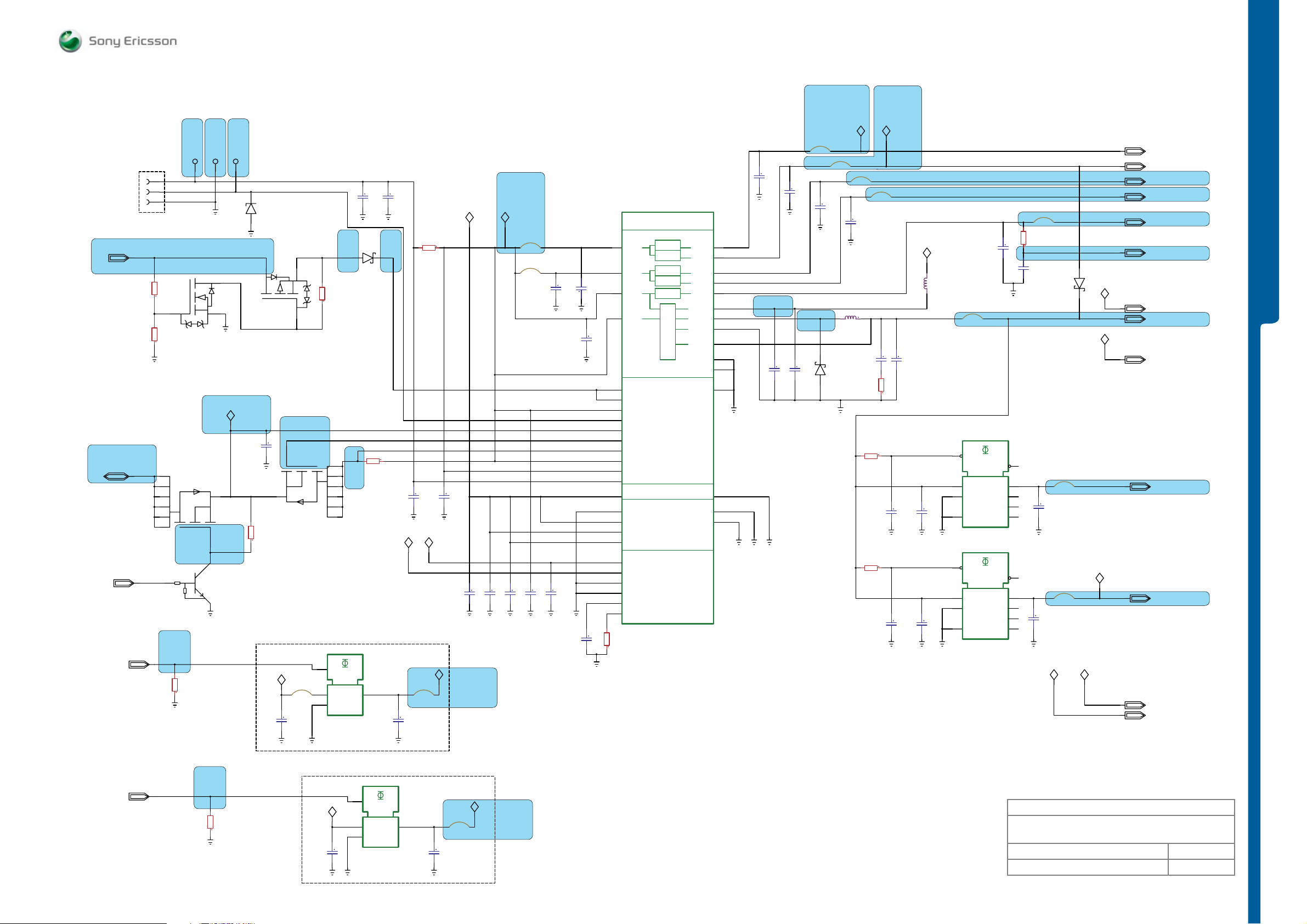
FUNCT I ON OVERVIEW
Baseband - Regulator s an d Ch ar gi ng
SEMC Electrical Repair Manual
K800 - K810
VBUS
DCIO
DCIO_ON
MP 130
Page 47
VBT_EN
220Kohms
R2234
100Kohms
X2200
MP 107
Page 47
R2235
SND10622
R1A
3
2
1
MP 13
Page
46
TP2220 TP2221 TP2222
V2220
G
2
RYN123919/1
NTJD4105C
V2203
8
RYN122684/2
7
6
3
2
1
Leadfree
1
MP 137
Page 47
1Mohms
R2209
MP 12
MP 11
Page
Page
46
46
V2200
6
SD
1
MP 128
DCIOint
Page 47
5
DCIOint
MP 127
Page 47
4
3
V2210
DTC114EM3T5G
RYN121916/2
2
VBT_EN
VBAT
BDATA
12
AC
3
RYN123919/1
NTJD4105C
V2220
C2201
1uF
<NM>
100Kohms
R2202
C2297
2.2uF
4
5
VBATI
MP 106
Page 47
VBUS_1
4
SD
100Kohms
R2233
5
G
MP 126
Page 47
V2202
RYN122684/2
ST2250
Strap
1
MP 28
2
Page
3
6
7
8
N2204
2
CE
14
21
IN
3
GND
R1115Z-281B-TR
RYT1137824/1
C2211
V2201
RKZ323907/1
46
OUT
22pF
Page 47
R2201
100mohms
C2212
3.3pF
MP 103
C2206
VCORE15
ST2219
12
Strap
C2296
4.7uF
R2200
25mohms
47pF
VDDE18
VBT27
C2207
47pF
VDIG
C2202
100nF
MP 134
Page 47
C2203
100nF
VBATI
MP 38
Page 46
ST2200
ST2201
C2205
22pF
C2209
100nF
C2210
100nF
21
21
C2200
4.7uF
C22117
100nF
VBUS_VINC
C2204
100nF
C2208
100nF
N2000
ERICSSON AB 2010
POWER
BASEBAND REGULATORS
M12
VBATB
A8
VBATF VDDF
A3
VBATC
E9
MOD1
F2
VBUS
F3
USBMOD
E1
VBATD
B11
BDATA
E2
VDCIO
D1
CHREG
D3
CHSENSE+
D2
CHSENSE-
F11
FGSENSE+
F12
FGSENSE-
M9
H9
DIGVSS
J8
DIGVDD
M5
VDDCODEC
M3
VDDBEAR
M10
VDDIO_18
C3
VDDIO
D10
SUB
D4
TEST
J12
VREF
H12
IREF
ROP1013066/6
100Kohms
R2203
LDO_D
LDO_E
LDO_F
LDO_G
LPREG
CONVERTER
BUCK
BATTERY MANAGEMENT
ANALOG BLOCK SUPPLY
AUDIO BLOCK SUPPLY
REF
R1A
Vincenne2
VDDD
VDDE
VDDG
VDDLP
VDDBUCK
SWBUCK
VSSBUCK
VBUCK
VSSB
VSSC
VSSD
VSSADCVDDADC
VSSCODEC
VSSBEAR
M11
L12
G3
B7
A9
L2
A2
A1
B1
B2
C6
E3
K8
K5
K4
VDD_D
VDD_E
VDD_F
VDD_G
VDDLP
VDDBUCK
SWBUCK
VBUCK
C2213
4.7uF
MP 26
Page 47
C2220
100nF
ST2202
12
C2214
4.7uF
MP 25
Page 47
C2219
10uF
RKZ123905/2
Local ground plane
MP 39
Page 46
ST2204
12
C2216
1uF
L2200
V2205
Leadfree
VDIG
ST2203
C2215
4.7uF
22uH
C2222
10uF
220mohms
R2205
R2212
1.8Kohms
R2213
4.7Kohms
21
ST2208
C22105
100nF
C22106
100nF
Page 46
VDDE18
MP 37
21
C2221
100nF
C2223
1uF
C2280
1uF
VBATI
L2201
ST2206
12
N2200
6
SHDN
1.3V
IN
9
EP
5
GND
MAX1976AETA-130
RYT1137810/1
N2201
6
SHDN
1.5V
IN
9
EP
5
GND
MAX1976AETA-150
RYT1137810/2
C2218
1uF
RESET
RESET
OUT
OUT
VDIG
VDDE18
VDDF13
VMSPICO
ST2205
21
4.7Kohms
R2204
+
C2217
RJE3551335/7
V2208
RKZ123905/1
<NM>
VCORE18
4
C2224
4.7uF
12
C2281
4.7uF
ST2207
ST2213
18
7
NC
2
NC
3
I.C
4
18
7
NC
2
NC
3
I.C
VBATI
DCIOint
21
VCORE15
VBT27VFM27
VRTC13
VBACKUP
VBATI
VCORE18
DCIOint
VCORE13
VCORE15
VBT27
VFM27
MP 29 Page 46
MP 33 Page 46
MP 58 Page 46
MP 51 Page 46
MP 24 Page 46
MP 56 Page 46
MP 100 Page 47
FUNCTION OVERVIEW
FM_EN
MP 76
Page 46
100Kohms
R2208
Bluetooth regulator
FM_EN
VBATI
C2293
1uF
FM Radio regulator
N2203
2
CE
IN
3
GND
R1115Z-281B-TR
RYT1137824/1
OUT
VFM27
41
ST2218
12
Strap
C2295
10uF
MP 77
Page 46
Made for
BASEBAND - Regulators & Charging
Document Nr Revision
2/1911 - ROA 128 1534/2 A
1202-3085 rev. 2
24 (121)
Page 25
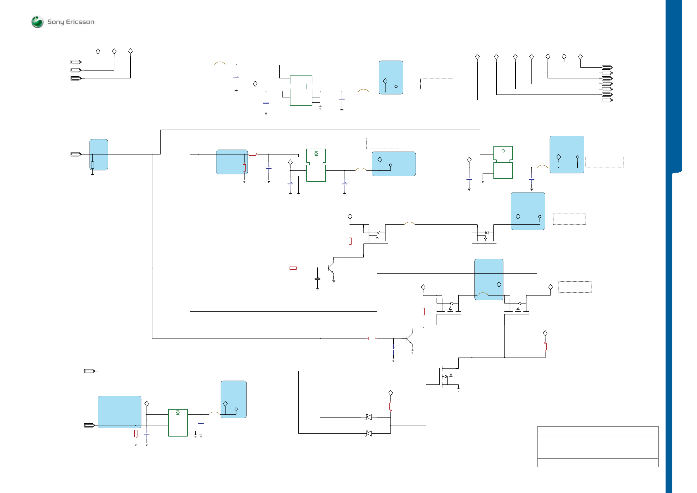
FUNCT I ON OVERVIEW
Baseband - Power Camera
SEMC Electrical Repair Manual
K800 - K810
VBATI
VCORE18
VDDE18
CAM_27_EN
R2207
100Kohms
VBATI VCORE18
MP 3
Page 46
CAM_27_EN
VDDE18
12
VCAMSD
ST2222
Strap
C22112
<NM>
MP 48
Page 46
V_VGAANAV_VGADIG
N2209_CE
N2209
3
6
5
N2202_CE
VBATI
C2290
1uF
R2227 15Kohms
CE
1
VOUT1
VDD1
VDD2
R1170D281B-TR
RYT1137822/1
2
VOUT2
4
GND
N2202
2
CE
14
OUT
IN
3
GND
R1115Z-281B-TR
RYT1137824/1
C22114
1uF
<NM>
CAM_27_EN
B
2
VCAMAF_1
C22110
10uF
C2292
100Kohms
C
V2211
E
1
VCAM27_1
10uF
VDDE18
R2229
K800
6
BC847BV
RYN121929/1
ST2227
12
Strap
Max current on VCAM27
ST2217
21
Strap
5167
S1 DS2
G
R2228 1 5Kohms
1uF
VBATI
C22109
10uF
R2232 15Kohms
C22111
1uF
R2231
100Kohms
Page 46
VCAMAF
70 mA.
VCAM27
RYN901926/1
FDJ1027P
V2212
C22113
1uF
<NM>
MP 90
TP2200
TP2201
MP 93
Page 46
ST2228
12
Strap
R2230
100Kohms
C
B
V2211
5
E
4
Max current on VCAMAF
VDDE18
3
BC847BV
RYN121929/1
310 mA.
CAM_27_EN
VCAMIO_1
4238
S1 DS2
RYN901926/1
FDJ1027P
V2212
G
C22115
1uF
VBATI
S1 DS2
RYN901926/1
FDJ1027P
615V2213
G
MP 46
Page 46
V_VGADIG
ST2229
12
Strap
VCAMSD_EN
N2210
2
CE
IN
3
GND
R1115Z-281B-TR
RYT1137824/1
7
OUT
24
3
41
VCAMIO
S1 DS2
RYN901926/1
FDJ1027P
V2213
G
C22116
MP 92
Page 46
10uF
8
TP2205
R2236
100Kohms
V_VGAANA
ST2230
12
Strap
VCAMSD
VCORE18
Max current on VCAMIO
VCAMAFVCAMIOVCAMSDVCAM27VCAM12
MP 95
Page 47
TP2204
20 mA.
Max current on VCAMSD
110 mA.
VCAMAF
VCAMIO
VCAMSD
VCAM27
VCAM12
V_VGAANA
V_VGADIG
Max current on V_VGAANA
50 mA.
FUNCTION OVERVIEW
CAMDIR
CAM_12_EN
MP 6
Page 46
CAM_12_EN
R2210
100Kohms
VBATI
N2205
13
VDD VOUT
4
ECO
6
CE
25
C2299
2.2uF
NC GND
R1161D121B-XX
RYT113962/1
ST2220
12
C22100
10uF
VCAM12
MP 89
Page 46
TP2202
CAMDIR
V2215
RKZ123905/1
V2216
RKZ123905/1
VDDE18
R2237
1Mohms
VCAMSD_EN_2
3
V2214
RYN123930/1
G
1
S D
2
NTK3043N
Made for
BASEBAND - Power Camera
Document Nr Revision
2/1911 - ROA 128 1534/2 A
1202-3085 rev. 2
25 (121)
Page 26
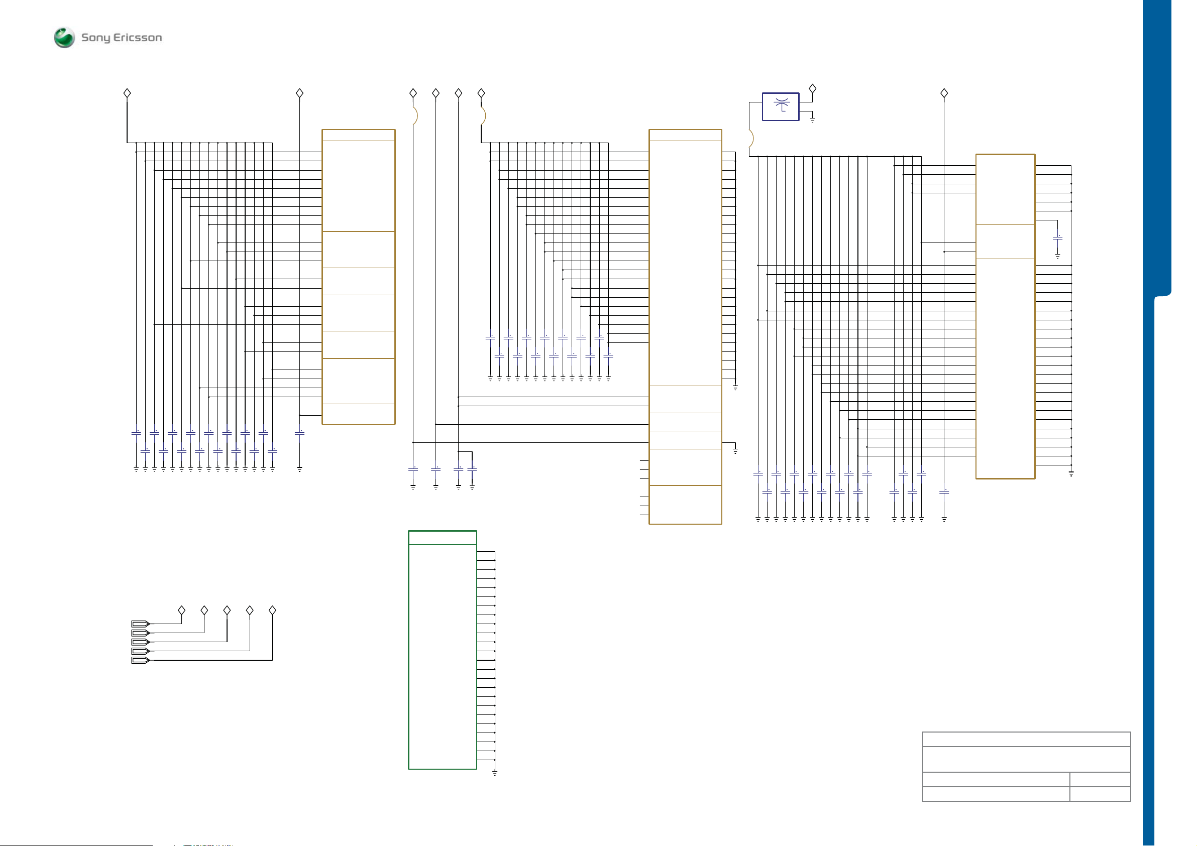
FUNCT I ON OVERVIEW
Baseband - Power ASICs
SEMC Electrical Repair Manual
K800 - K810
VCORE13
VDDE18
VDDF13
VRTC13
VCORE13
VCORE15
C2225
100nF
C2233
C2231
C2229
100nF
100nF
100nF C2230
C2232
100nF
100nF
100nF C2227
C2228
100nF
100nF C2226
VDDE18 VDDF13 VRTC13 VCORE13 VCORE15
C2234
100nF
C2235
100nF
C2236
100nF
100nF C2237
C2238
100nF
C2239
100nF
C2240
100nF
VDDF13
C2241
100nF
D2000
MARIKA_POWER_CORE
M1
VDDC0
T1
VDDC1
AA11
VDDC2
AA16
VDDC3
U21
VDDC4
K21
VDDC5
A12
VDDC6
A10
VDDC7
A6
VDDC8
H21
VDDCARM0
A17
VDDCARM1
A13
VDDCARM2
P21
VDDCTCM0
L21
VDDCTCM1
U1
VDDCGSM0
AA4
VDDCGSM1
AA10
VDDCGSM2
N1
VDDCRAM0
R1
VDDCRAM1
F1
VDDCUMA0
L1
VDDCUMA1
A9
VDDCUMA2
A5
VDDCUMA3
AA19
VDDCPLL
DB2021_MARIKA P2A
ROP1013083/1
Core-1.3V
ARMCore-1.3V
TCMCore-1.3V
GSMCore-1.3V
RAMCore-1.3V
UMACore-1.3V
DPLL-1.3V
VRTC13
12
ST2211
C2256
100nF C2257
100nF
N2000
ERICSSON AB 2010
POWER
THERMAL GROUNDS
ERICSSON_AB2012
ROP1013066/6
R1A
VCORE15
C2258
100nF
VSSTH1
VSSTH2
VSSTH3
VSSTH4
VSSTH5
VSSTH6
VSSTH7
VSSTH8
VSSTH9
VSSTH10
VSSTH11
VSSTH12
VSSTH13
VSSTH14
VSSTH15
VSSTH17
VSSTH18
VSSTH19
VSSTH21
VSSTH22
VSSTH25
VSSTH26
VSSTH27
VSSTH30
VDDE18
C2259
100nF
C2262
100nF
GND
100nF C2263
IN
1uF
C2264
100nF
VCORE15
23
1
100nF
C2265
100nF
C2266
C2267
100nF
C2268
100nF
C2269
100nF
C2270
100nF
C2271
100nF
C2272
100nF
C2273
100nF
100nF C2274
C2278
12
ST2210
100nF C2251
100nF C2252
C2253
100nF
C2254
100nF
C2255
100nF
C2248
C2246
100nF C2242
100nF C2244
C2243
100nF
F7
G7
G6
E5
E6
E7
E8
F8
G8
H8
H7
H6
H5
G5
F5
D6
D7
D8
F9
G9
J7
J6
J5
F4
100nF C2245
100nF
C2247
100nF
100nF
100nF C2250
100nF C2249
D2000
MARIKA_POWER_OTHER
C1
D1
G1
K1
P1
V1
AA3
AA6
AA9
AA14
R21
N21
J21
G21
D21
A20
A18
A15
A11
A8
A4
A3
AA18
Y21
Y17
V13
V16
AA21
W18
AA1
A21
A1
I/O-1.8V
VDDEE00
VDDEE01
VDDEE02
VDDEE03
VDDEE04
VDDEE05
VDDEE06
VDDEE07
VDDEE08
VDDEE09
VDDEE10
VDDEE11
VDDEE12
VDDEE13
VDDEE14
VDDEE15
VDDEE16
VDDEE17
VDDEE18
VDDEE19
VDDEE20
VDDEE21
I/O-1.5/1.8V
VDDEWL0
VDDEWL1
RTC-1.3V
VDDRTC
Analog-1.3V
VDDA
Efuse
VPPSTD0
VPPSTD1
VPPSTDSENSE
NotConnected_Balls
NC_RSV0
NC_RSV1
NC_RSV2
DB2021_MARIKA_SECURITY_EFUSE
ROP1013083/4 R2A
VSS00
VSS01
VSS02
VSS03
VSS04
VSS05
VSS06
VSS07
VSS08
VSS09
VSS10
VSS11
VSS12
VSS13
VSS14
VSS15
VSS16
VSS17
VSS18
VSS19
VSS20
VSS21
VSS22
VSS23
VSS24
VSS25
VSSA
G4
J4
L4
M4
P4
T4
V5
V6
V9
V11
W14
V14
V18
T18
N18
M18
K18
H18
E18
D17
D14
D12
D10
D9
D7
D5
Y15
OUT
REV501107/201
ST2212
21
C2260
100nF
C2261
100nF
VRTC13VDDF13
D2001
EMP_WANDA_POWER
U6
VDD_TX
U10
VDD_RX
R11
VDD_BG
VDD_CS_ADPLL
VSSCOMPLEX_IO1
VSSCOMPLEX_IO2
DIGITAL SUPPLY
VDD_DPLL
VDD_CLK32
VDD_1
VDD_2
VDD_3
VDD_4
VDD_5
VDD_6
VDD_7
VDD_8
VDD_9
VDD_10
VDD_11
VDD_12
VDD_13
VDD_14
VDD_15
VDD_16
VDD_17
VDD_18
VDD_19
VDD_20
VDD_21
VDD_22
ROP1013044/4
VSS_CS_ADPLL
C2275
100nF
C2276
100nF
R12
L15
T17
A3
A6
A12
A17
B14
B8
B1
D2
D16
F17
G1
H17
K17
K2
M1
N17
R1
R13
R16
T2
U5
U16
C2277
100nF
Made for
BASEBAND - Power ASICs
R1A
VSS_TX
VSS_RX
VSS_BG
BG_REF
VSS_1
VSS_2
VSS_3
VSS_4
VSS_5
VSS_6
VSS_7
VSS_8
VSS_9
VSS_10
VSS_11
VSS_12
VSS_13
VSS_14
VSS_15
VSS_16
VSS_17
VSS_18
VSS_19
VSS_20
VSS_21
VSS_22
VSS_23
R8
T8
T11
N11
T6
T12
U11
C2279
100nF
B15
B11
B10
B7
C3
C5
C12
C16
D3
F3
F15
H3
H16
J16
L2
L16
N3
P16
R3
R4
T4
U15
U17
FUNCTION OVERVIEW
Document Nr Revision
2/1911 - ROA 128 1534/2 A
1202-3085 rev. 2
26 (121)
Page 27
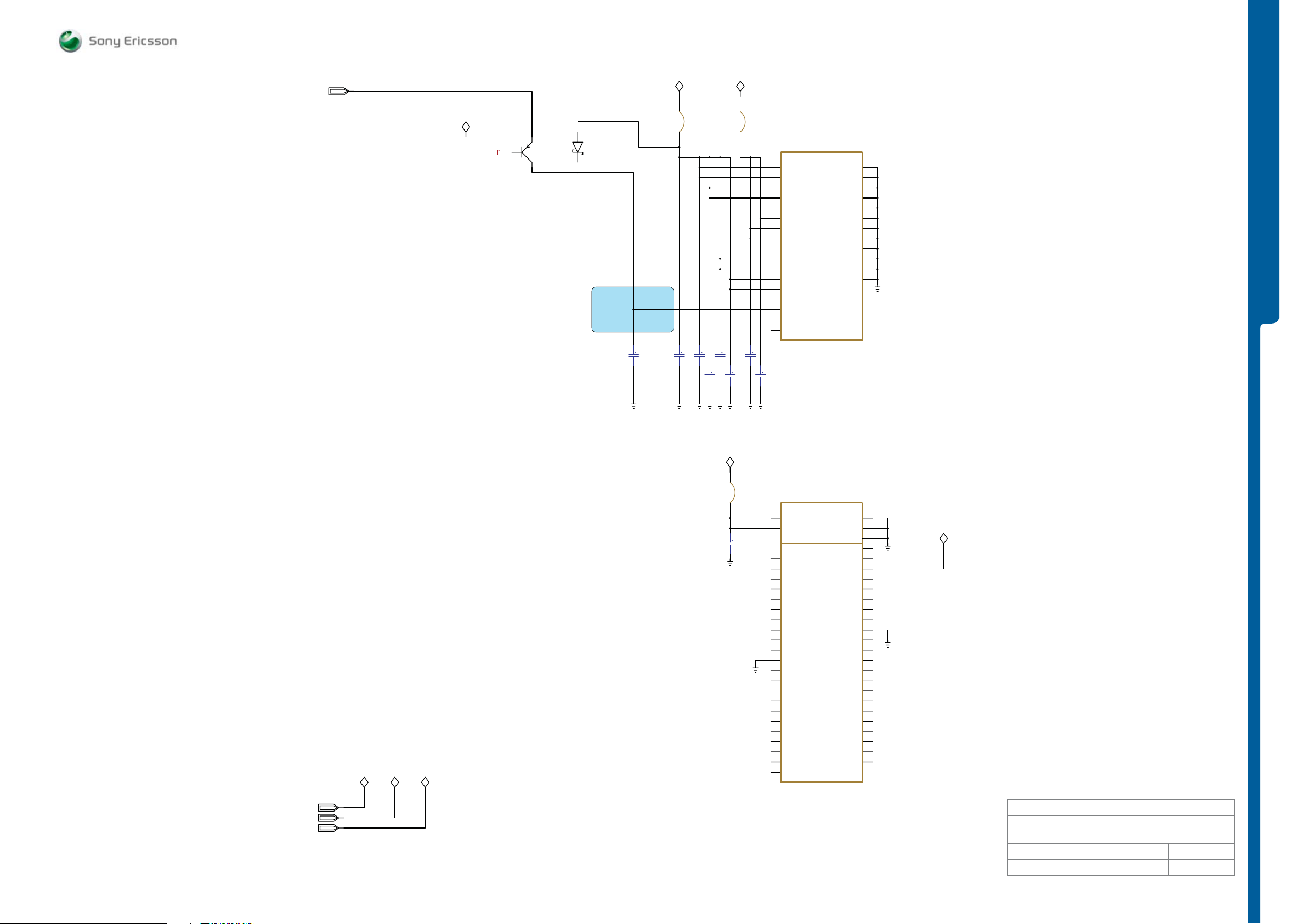
VPP
FUNCT I ON OVERVIEW
VBATI
E
1KohmsR2206
V2206
B
RYN120903/1
C
V2207
RKZ123905/1
MP 64
Page 46
Baseband - Power Memories
VDDE18 VCORE18
FLASH_VPP
C2298
220nF
12
ST2231
VDDE18_NOR VCORE18_NOR
C2283
4.7uF C2282
100nF
C2284
100nF
C2285
100nF
C2286
100nF
12
ST2232
C2287
100nF
C2288
100nF
D2300
D4
F-VCC
D6
F-VCC
J4
F-VCC
J6
F-VCC
D3
D-VCC
C5
D-VCC
D7
D-VCC
J2
VCCQ
J3
VCCQ
J7
VCCQ
J8
VCCQ
J1
F-VPP
D2
S-VCC
PF38F4060L0YTB0
RYT118953/1
X16D_POWER
VSS
VSS
VSS
VSS
VSS
VSS
VSS
VSS
VSS
VSS
VSS
VSS
SEMC Electrical Repair Manual
K800 - K810
C2
C3
C4
C6
C7
C8
K2
K3
K4
K6
K7
K8
FUNCTION OVERVIEW
VCORE18 VDDE18
VBATI
VDDE18
100nF C2289
ST2216
2 1
D2301
32Mx8Bit-NAND_FLASH_POW
F6
G4
B1
B4
B5
B6
C1
C2
C3
C4
C5
C6
D1
D2
D3
1
2
3
4
5
6
7
8
POWER/GND
VCC
VCCQ
NC
NC
NC
NC
NC
NC
NC
NC
NC
NC
NC
NC
NC
SUPPORTPINS
DNU
DNU
DNU
DNU
DNU
DNU
DNU
DNU
K9F1208R0B-JIB
RYT118932/2
AND NC
VSS
VSS
VSS
DNU
DNU
DNU
DNU
DNU
DNU
DNU
H1
H6
A3
D4
NC
D5
NC
D6
NC
E1
NC
E2
NC
E3
NC
E4
NC
E5
NC
E6
NC
F1
NC
F3
NC
F4
NC
F5
NC
G1
NC
G3
NC
9
10
11
12
13
14
15
VCORE18
VCORE18
VDDE18
VBATI
Made for
BASEBAND - Power Memories
Document Nr Revision
2/1911 - ROA 128 1534/2 A
1202-3085 rev. 2
27 (121)
Page 28
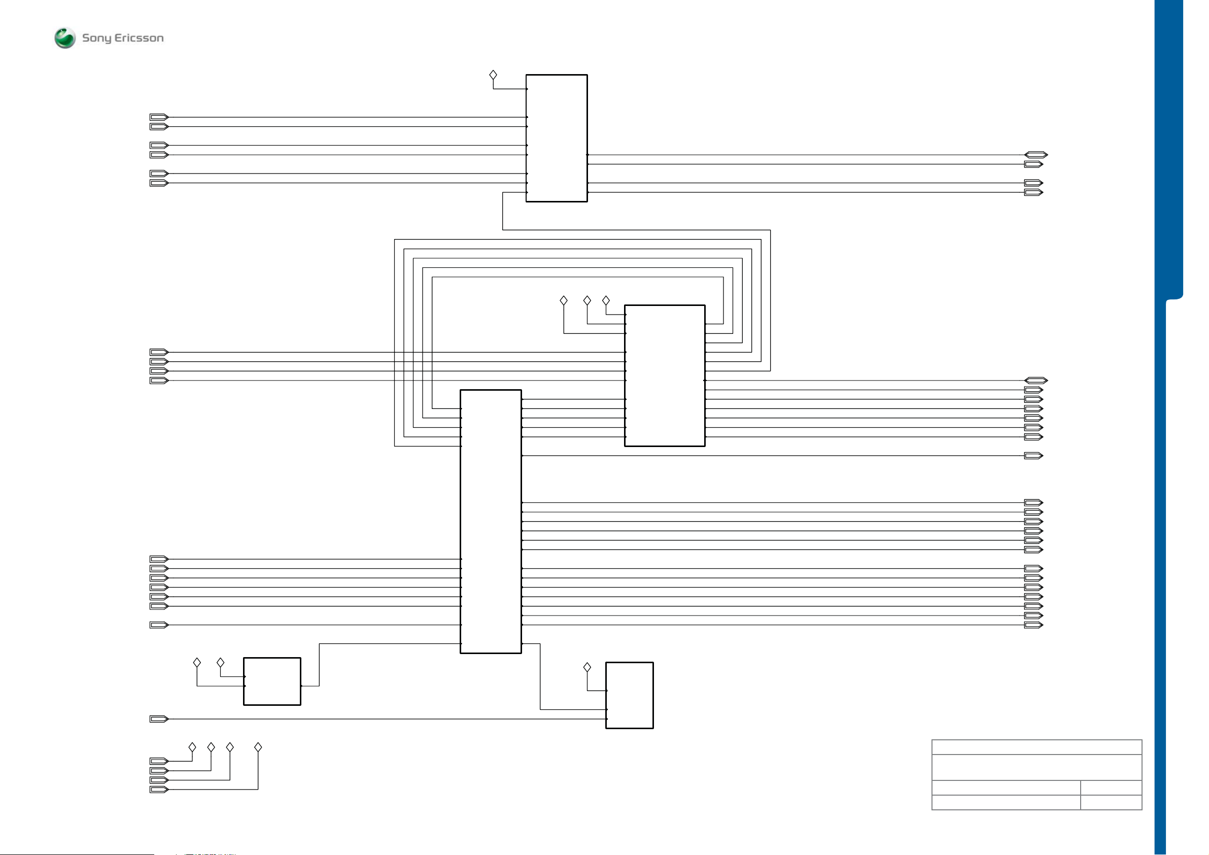
FUNCT I ON OVERVIEW
Baseband - Operat io n an d S ervices Top
SEMC Electrical Repair Manual
K800 - K810
VDDE18
SPL
SPR
RTEMP
VLOOP
WRFLOOP
VAD
VBACKUP
OPTOTEMP
Page 30
IRRXD
CTMS
DTMS
USBRCV
USBVALID
EDB_EN
IRTXD
IRSD
CFMS_AID
DFMS
CAMDIR
RTEMP
VLOOP
WRFLOOP
VAD I2CDAT1
VBACKUP
OPTOTEMP
MIDREF
SPL
SPR
FLASH_STROBE
MIDREF
FLASH_STROBE
Page 31
VDDE18
RTEMP
VLOOP
WRFLOOP
VAD
VBACKUP
OPTOTEMP
AID_AD
ADC/DAC & MP-PCM & I2C
ADC/DAC & MP-PCM & I2C
I2CDAT1
I2CCLK1
WPABIAS
VCXOCONT
EDB_EN
IRTXD
IRSD
CFMS_AID
DFMS
I2CDAT1
I2CCLK1
WPABIAS
VCXOCONT
AID_AD
USBVALID
USBRCV
DTMS
CTMS
IRRXD
VDIGVDDE18
VBATI
Page 33
VBATI
VDIG
VDDE18
MIDREF
SPL
SPR
FLASH_STROBE
EDB_EN
IRTXD
IRSD
CFMS_AID
DFMS
Connectivity
Connectivity
IRRXD
CTMS
DTMS
USBRCV
USBVALID
AID_AD
DCIO
MICN/AUXinR
MICP/AUXinL
FM_ANTENNA
VBUS
VPP
SERVICEn
DCIO
MICN/AUXinR
MICP/AUXinL
FM_ANTENNA
VBUS
VPP
SERVICEn
CAMDIR
I2CCLK1
WPABIAS
VCXOCONT
DCIO
MICN/AUXinR
MICP/AUXinL
FM_ANTENNA
VBUS
VPP
SERVICEn
CAMDIR
FUNCTION OVERVIEW
CAMIRQ
CHARGE_RDY
LIDSENSE
BTRX
BTCTS
BTCLKREQ
FMINT
MEMRESn
VBATI
VDIG
VDDE18
VMSPICO
VBATI VDIG
STROBE_ENABLE
LKEYBRGT
UKEYBRGT
FOCUSLED_ON
CHARGE_ON
CAMIRQ
CHARGE_RDY
LIDSENSE
BTRX
BTCTS
BTCLKREQ
FMINT
MSDETECT
VDDE18
Page 32
VMSPICO
VDDE18
SIM & MS Pico
SIM & MS Pico
VMSPICO
MSDETECT
MEMRESn MEMRESn
VMSPICOVDDE18
CAMIRQ
CHARGE_RDY
LIDSENSE
BTRX
BTCTS
BTCLKREQ
FMINT
MSDETECT
GPIO
GPIO
AMPCTRL
VBT_EN
CAM_12_EN
CAM_27_EN
FM_EN
BTTX
BTRTS
DCIO_ON
MEMDPD
MEMDPD
VDDE18
Page 29
VDDE18
MEMDPD
MEMRESn
Memories
Memories
STROBE_ENABLE
LKEYBRGT
UKEYBRGT
FOCUSLED_ON
CHARGE_ON
AMPCTRL
VBT_EN
CAM_12_EN
CAM_27_EN
FM_EN
BTTX
BTRTS
DCIO_ON
STROBE_ENABLE
LKEYBRGT
UKEYBRGT
FOCUSLED_ON
CHARGE_ON
AMPCTRL
VBT_EN
CAM_12_EN
CAM_27_EN
FM_EN
BTTX
BTRTS
DCIO_ON
Made for
BASEBAND - Operation & Services Top
Document Nr Revision
2/1911 - ROA 128 1534/2 A
1202-3085 rev. 2
28 (121)
Page 29
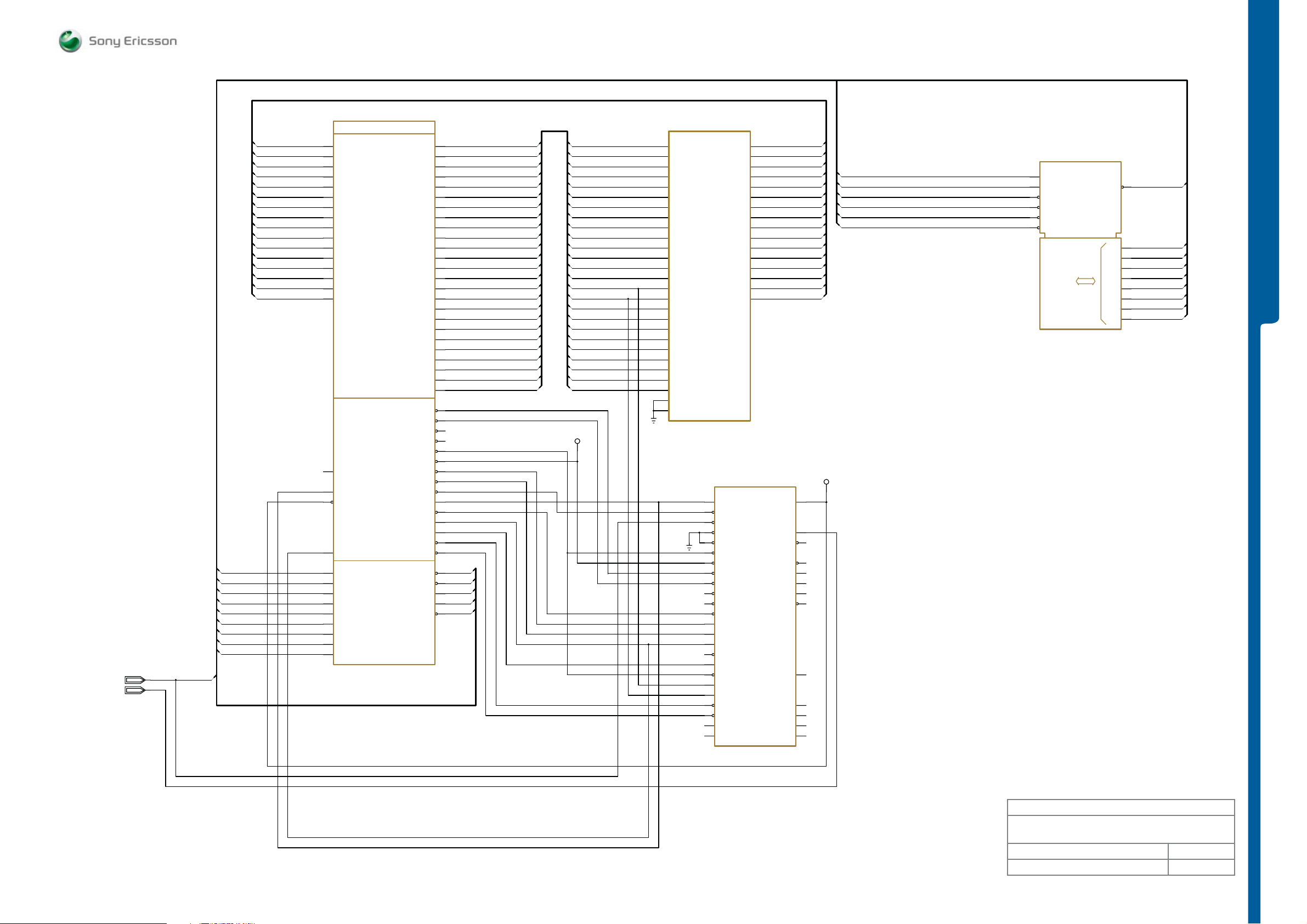
MEMRESn
MEMDPD
MEMRESn
NF_D[0]
NF_D[1]
NF_D[2]
NF_D[3]
NF_D[4]
NF_D[5]
NF_D[6]
NF_D[7]
NF_RB
EMIF_DATA[0]
EMIF_DATA[1]
EMIF_DATA[2]
EMIF_DATA[3]
EMIF_DATA[4]
EMIF_DATA[5]
EMIF_DATA[6]
EMIF_DATA[7]
EMIF_DATA[8]
EMIF_DATA[9]
EMIF_DATA[10]
EMIF_DATA[11]
EMIF_DATA[12]
EMIF_DATA[13]
EMIF_DATA[14]
EMIF_DATA[15]
MEM_CLK
SDR_CLK
D2000
MARIKA_MEMORY
B17
B16
C15
B15
C14
B14
C13
B13
C12
B12
C11
B11
C10
B10
C9
B9
E5
C6
C8
B6
D2
E1
G3
H8
E2
H4
H3
F2
K3
Data_and_Address_Bus
D0
D1
D2
D3
D4
D5
D6
D7
D8
D9
D10
D11
D12
D13
D14
D15
Memory_Control
VINITHI
MEMCLKRET/PSR_CLKRET
MEMWAIT_N
SDR_CLKRET
NF_D0
NF_D1
NF_D2
NF_D3
NF_D4
NF_D5
NF_D6
NF_D7
NF_R/B
DB2021_MARIKA_SECURITY_EFUSE
ROP1013083/4 R2A
MEMBE0_N/SDR_DQML
MEMBE1_N/SDR_DQMU
NAND-Flash_IF
A15/SDR_BS0
A16/SDR_BS1
A25/CRE
CS0_N
CS1_N
CS2_N
CS3_N
WE_N
OE_N
MEMADV_N
MEMCLK/PSR_CLK
SDR_CS_N
SDR_CLK
SDR_CKE
SDR_CAS_N
SDR_RAS_N
NF_RE_N
NF_WE_N
NF_ALE
NF_CLE
NF_CS_N
FUNCT I ON OVERVIEW
EMIF_DATA[0:15]
EMIF_ADDRESS[1:25]
H14
A1
A16
A2
G14
A3
A14
A4
D13
A5
G13
A6
H13
A7
G12
A8
H12
A9
D11
A10
G11
A11
H11
A12
G10
A13
H10
A14
A7
G9
B5
A17
C5
A18
D8
A19
G8
A20
B4
A21
H9
A22
B3
A23
A2
A24
D6
E4
E3
F4
F3
B2
C3
C4
D4
B18
C7
B1
B8
B7
D3
SDR_CASn
C2
SDR_RASn
H7
NF_REn
G2
NF_WEn
H1
NF_ALE
J3
NF_CLE
H2
NF_CSn
MEMWAITn
MEMRESn
MEMDPD
EMIF_ADDRESS[1]
EMIF_ADDRESS[2]
EMIF_ADDRESS[3]
EMIF_ADDRESS[4]
EMIF_ADDRESS[5]
EMIF_ADDRESS[6]
EMIF_ADDRESS[7]
EMIF_ADDRESS[8]
EMIF_ADDRESS[9]
EMIF_ADDRESS[10]
EMIF_ADDRESS[11]
EMIF_ADDRESS[12]
EMIF_ADDRESS[13]
EMIF_ADDRESS[14]
EMIF_ADDRESS[15]
EMIF_ADDRESS[16]
EMIF_ADDRESS[17]
EMIF_ADDRESS[18]
EMIF_ADDRESS[19]
EMIF_ADDRESS[20]
EMIF_ADDRESS[21]
EMIF_ADDRESS[22]
EMIF_ADDRESS[23]
EMIF_ADDRESS[24]
EMIF_ADDRESS[25]
CS0n
CS1n
WEn
OEn
MEM_BE0n
MEM_BE1n
MEM_ADVn
MEM_CLK
SDR_CSn
SDR_CLK
SDR_CKE
NANDBUS
EMIF_ADDRESS[1]
EMIF_ADDRESS[2]
EMIF_ADDRESS[3]
EMIF_ADDRESS[4]
EMIF_ADDRESS[5]
EMIF_ADDRESS[6]
EMIF_ADDRESS[7]
EMIF_ADDRESS[8]
EMIF_ADDRESS[9]
EMIF_ADDRESS[10]
EMIF_ADDRESS[11]
EMIF_ADDRESS[12]
EMIF_ADDRESS[13]
EMIF_ADDRESS[14]
EMIF_ADDRESS[15]
EMIF_ADDRESS[16]
EMIF_ADDRESS[17]
EMIF_ADDRESS[18]
EMIF_ADDRESS[19]
EMIF_ADDRESS[20]
EMIF_ADDRESS[21]
EMIF_ADDRESS[22]
EMIF_ADDRESS[23]
EMIF_ADDRESS[24]
EMIF_ADDRESS[25]
SP2333
SDR_CKE
Baseband - Operat io n an d S ervices Me m ories
D2300
D1
A1
C1
A2
B1
A3
B2
A4
A2
A5
B3
A6
A3
A7
A4
A8
G8
A9
F8
A10
E8
A11
G9
A12
F9
A13
E9
A14
D9
A15
C9
A16
B9
A17
B4
A18
B5
A19
A5
A20
F7
A21
E7
A22
B7
A23
A6
A24
A7
A25
A8
A26
B8
A27
PF38F5060M0Y0B0
RYT118953/1
X16D_IO
D2300
K5
D5
G7
E1
F1
E2
H7
G3
G2
H3
E6
F2
H9
H8
J5
H5
G6
H6
G4
H4
F3
F4
M7
M3
PF38F4060L0YTB0
RYT118953/1
F-CLK
F-ADV
F-RST
F-WP1
F-WP2
F-WE
F-OE
F1-CE
F2-CE
F3-CE
F4-CE/A28
D1-CS
D-DM0
D-DM1
D-CLK
/D-CLK
D-CKE
D-WE
D-BA0
D-BA1
D-CAS
D-RAS
D-UDQS
D-LDQS
M2
DQ0
L1
DQ1
K1
DQ2
L2
DQ3
M4
DQ4
L3
DQ5
L4
DQ6
L5
DQ7
M5
DQ8
L6
DQ9
M6
DQ10
L7
DQ11
L8
DQ12
K9
DQ13
L9
DQ14
M8
DQ15
X16D_CONTROL
WAIT
NC_F-DPD
NC_D2-CS
NC_S-CS1
NC_S-CS2
NC_N-ALE
NC_N-CLE
NC_N-RY/BY
RFU
DU_1
DU_2
DU_3
DU_4
EMIF_DATA[0]
EMIF_DATA[1]
EMIF_DATA[2]
EMIF_DATA[3]
EMIF_DATA[4]
EMIF_DATA[5]
EMIF_DATA[6]
EMIF_DATA[7]
EMIF_DATA[8]
EMIF_DATA[9]
EMIF_DATA[10]
EMIF_DATA[11]
EMIF_DATA[12]
EMIF_DATA[13]
EMIF_DATA[14]
EMIF_DATA[15]
J9
B6
E3
F6
H2
D8
E5
H1
G1
A1
A9
M1
M9
NF_CLE
NF_ALE
NF_CSn
NF_REn
NF_WEn
MEMRESn
SP2319
D2301
32Mx8Bit-NAND_FLASH_IF
B3
CLE
A2
ALE
A4
CE
B2
RE
A5
WE
A1
WP
K9F1208R0B-JIB
RYT118932/2
SEMC Electrical Repair Manual
K800 - K810
NF_RB
NF_D[0]
NF_D[1]
NF_D[2]
NF_D[3]
NF_D[4]
NF_D[5]
NF_D[6]
NF_D[7]
DATA
R/B
IO_0
IO_1
IO_2
IO_3
IO_4
IO_5
IO_6
IO_7
A6
F2
G2
H2
H3
H4
G5
H5
G6
FUNCTION OVERVIEW
SDR_CLK
MEM_CLK
Made for
BASEBAND - Operation & Sevices Memories
Document Nr Revision
2/1911 - ROA 128 1534/2 A
1202-3085 rev. 2
29 (121)
Page 30
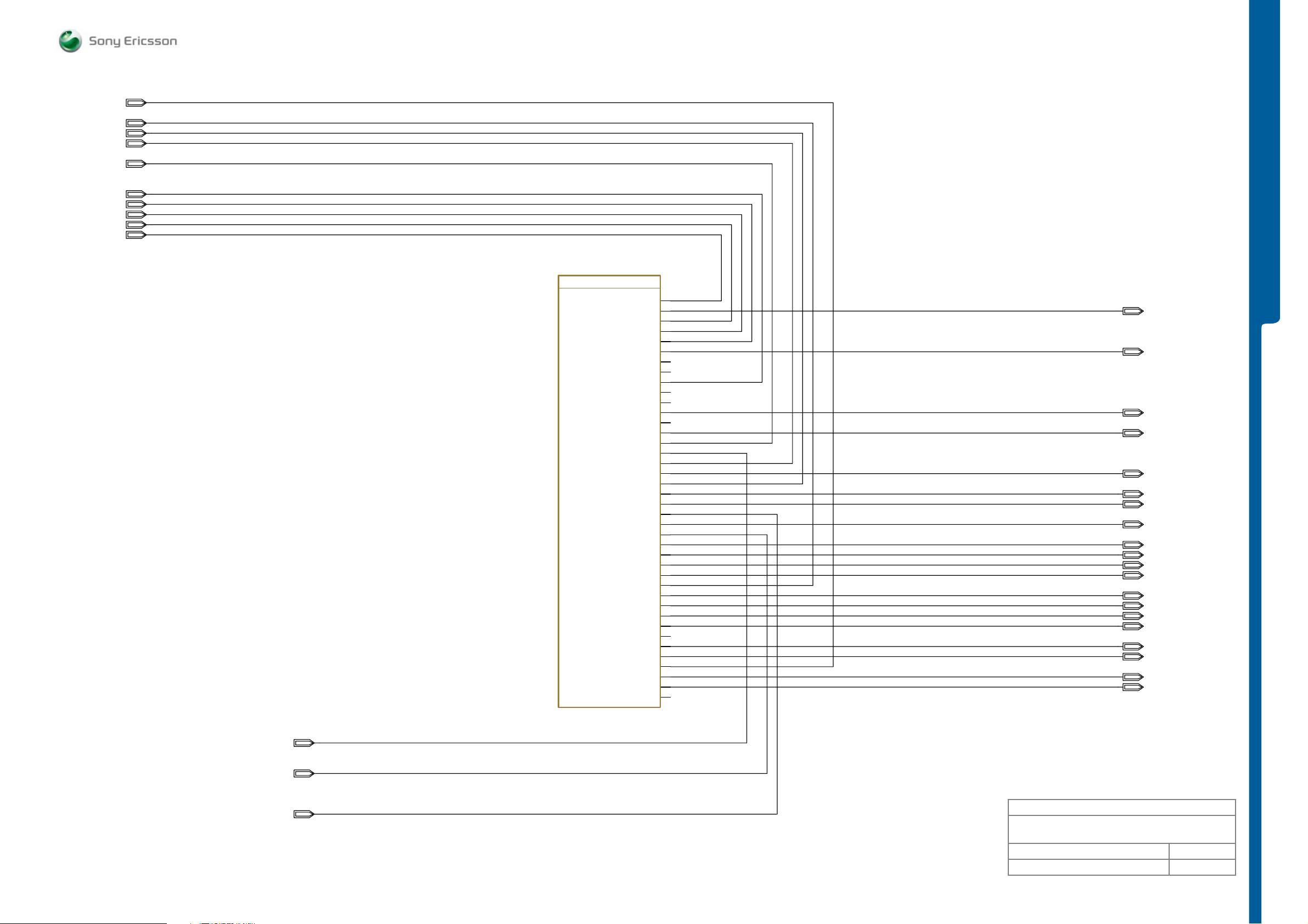
FUNCT I ON OVERVIEW
Baseband - Operat io n an d S e rvices GPIO
SEMC Electrical Repair Manual
K800 - K810
IRRXD
MSDETECT
BTCTS
BTRX
FMINT
BTCLKREQ
CTMS
USBVALID
USBRCV
DTMS
IRRXD
MSDETECT
BTCTS
BTRX
FMINT
BTCLKREQ
CTMS
USBVALID
USBRCV
DTMS
D2000
DB2021_MARIKA_SECURITY_EFUSE
ROP1013083/4 R2A
MARIKA_GPIO
Gen.Purpose_I/O
GPIO00/UARTRX0
GPIO01/UARTTX0
GPIO02/UARTCTS0/USBRCV
GPIO03/UARTRTS0/USBVBUS
GPIO04/UARTRX1
GPIO05/UARTTX1
GPIO06/UARTCTS1
GPIO07/UARTRTS1
GPIO10/SYSCLKREQ0
GPIO11/SYSCLKREQ1
GPIO12/SYSCLKREQ2
GPIO13/GPSSTART
GPIO15/EXTTRIG
GPIO16/BUS_REQ
GPIO17/BUS_GNT
GPIO20/UARTRX3/DSPGPIO0
GPIO21/UARTTX3/DSPGPIO1
GPIO22/UARTCTS3/DSPGPIO2
GPIO23/UARTRTS3/DSPGPIO3
GPIO24/UARTRX6/SPIDI/DSPGPIO4
GPIO25/UARTTX6/SPIDO/DSPGPIO5
GPIO26/UARTCTS6/SPIRDY/DSPGPIO6
GPIO27/UARTRTS6/SPICLK/DSPGPIO7
GPIO41/JOGYB/SPIEN1/UARTCTS0
GPIO42/JOGYS/SPIEN2/UARTRTS0
GPIO43/TGBUZZ/SPIEN3/IRSELECT
GPIO45/UARTTX6/IRTX/RCTX
GPIO47/UARTRTS6/RCTX/RC
GPIO30/FM
GPIO31/PWM0
GPIO32/PWM1
GPIO33/MMCPOW
GPIO34/MCCLKRET
GPIO35/JOGXA
GPIO36/JOGXB
GPIO37/JOGXS
GPIO40/JOGYA/SPIEN0
GPIO44/UARTRX6
GPIO46/UARTCTS6/IRSD
GPIO14
R3
P7
T3
V2
R4
W1
N8
W2
Y1
Y2
U4
W3
V3
V4
AA2
Y3
W5
W4
W6
V7
Y4
AA5
W7
P8
Y5
V8
W8
Y6
R8
AA7
Y7
AA8
W9
Y8
W10
R9
P9
Y9
V10
W11
DTMS
DFMS
USBRCV
USBVALID
CTMS
CFMS_AID
BTCLKREQ
CHARGE_ON
AMPCTRL
FMINT
CHARGE_RDY
BTRX
BTTX
BTCTS
BTRTS
CAM_12_EN
CAMIRQ
CAMDIR
LIDSENSE
DCIO_ON
LKEYBRGT
UKEYBRGT
VBT_EN
MSDETECT
CAM_27_EN
FM_EN
FOCUSLED_ON
MEMDPD
EDB_EN
STROBE_ENABLE
IRRXD
IRTXD
IRSD
FUNCTION OVERVIEW
DFMS
CFMS_AID
CHARGE_ON
AMPCTRL
BTTX
BTRTS
CAM_12_EN
CAMDIR
DCIO_ON
LKEYBRGT
UKEYBRGT
VBT_EN
CAM_27_EN
FM_EN
FOCUSLED_ON
MEMDPD
EDB_EN
STROBE_ENABLE
IRTXD
IRSD
CHARGE_RDY
LIDSENSE
CAMIRQ
Made for
BASEBAND - Operation & Services GPIO
Document Nr Revision
2/1911 - ROA 128 1534/2 A
1202-3085 rev. 2
30 (121)
Page 31

RTEMP
VLOOP
WRFLOOP
VAD
VBACKUP
OPTOTEMP
AID_AD
SP2350 SP2351
D2001
EMP_WANDA_OP
ADC_DAC IF
ROP1013044/4
DACCLK
DACDAT
DACSTR
ADCSTR
ACC_STR
DAC_DAT
DAC_STR
DAC_CLK
R1A
M16
L13
M15
N15
RTEMP
VLOOP
WRFLOOP
VAD
VBACKUP
OPTOTEMP
AID_AD
ADCSTR
FUNCT I ON OVERVIEW
Baseband - Oper at ion a n d Se rvices A DC & DAC
N2000
ERICSSON AB 2010
OP AND SERVICES
ADC
L10
GPA1
K10
GPA2
L11
GPA3
K11
GPA4
K12
GPA5
J11
GPA6
J10
GPA7
J9
GPA12
D9
GPA13
C7
ADSTR
ERICSSON_AB2012
ROP1013066/6
N2000
C9 B5
A10
C8
B9
ERICSSON_AB2012
ROP1013066/6
ERICSSON AB 2010
OP AND SERVICES
DAC
DACDAT
DACCLK
DACSTR
I2C IF
SDA
SCL
R1A
R1A
DACO1
DAC02/4
DACO3
G11
H11B10
WPABIAS
VCXOCONT
SEMC Electrical Repair Manual
K800 - K810
FUNCTION OVERVIEW
WPABIAS
VCXOCONT
VDDE18
D2000
MARIKA_I2C_IF
DB2021_MARIKA_SECURITY_EFUSE
ROP1013083/4
D2000
MARIKA_DAC_IF
DB2021_MARIKA_SECURITY_EFUSE
ROP1013083/4
I2CSCL0
I2CSDA0
I2CSCL1
I2CSDA1
DACCLK
DACDAT
DACSTR
ADCSTR
M19
N15
V15
Y18
W16
AA20
VDDE18
10Kohms
R2311
N2
M3
ST2301
10Kohms
R2312
21
3.3Kohms
R2313
MP 65
Page 46
VDDE18
Page 46
MP 66
3.3Kohms
R2314
I2CCLK1
I2CDAT1
I2CCLK1
I2CDAT1
VDDE18
Made for
BASEBAND
Operation & Services ADC & DAC
Document Nr Revision
2/1911 - ROA 128 1534/2 A
1202-3085 rev. 2
31 (121)
Page 32

FUNCT I ON OVERVIEW
VMSPICO
Baseband - Oper at ion a n d Se rvices MS Pico & SIM
VDDE18
SEMC Electrical Repair Manual
K800 - K810
D2000
MARIKA_CARD_IF
MemoryCard_IF
MSSDIO0/MMCDAT0
MSSDIO1/MMCDAT1
MSSDIO2/MMCDAT2
MSSDIO3/MMCDAT3/CD
MSSCLK/MMCCLK
MSBS/MMCCMD
MSBSDIR/MMCCMDDIR
MSSDIODIR/MMCDATDIR
SIM_IF
SIMRST_N
DB2021_MARIKA_SECURITY_E FUSE
ROP1013083/4
SIMCLK
SIMDAT
C2309
1uF
10Kohms
R2308
C2332
1uF
V2302
RKZ123905/1
<NM>
C2330
33pF
1Mohms
R2305
SIMCLK_2
R2306
R2307
MSDETECT
0ohms
0ohms
C2310
22pF
MP 124
Page
47
C2311
22pF
SIMVCC
SIMRSTn
SIMCLK
MP 123
Page
47
C2312
22pF
MP 125
Page
47
C2313
1nF
SIMDAT
MP 129
Page
47
C23141uF
MP 96 Page 47
X2302
1
SIMVCC
2
SIMCONRST
3
SIMCONCLK
5
GND
6
NC
7
SIMCONDAT
CCM03-3801
RNK87146
MSDETECT
R2A
FUNCTION OVERVIEW
X2301
L7
L2
L8
M2
K8
K2
K7
L3
N14
M21
N20
MSSDIO0
MSSDIO1
MSSDIO2
MSSDIO3
MSSCLK
MSBS
C2307
100Kohms
R2328
<NM>
22pF
N2000
C2
SIMOFF
H2
SRST
J3
SCLK
H1
SDAT
ERICSSON_AB2012
ROP1013066/6
100Kohms
100Kohms
R2324
R2327
100Kohms
R2325
VDDE18
SP2334 SP2335
R2326
10Kohms
SIMRSTn_1
SIMCLK_1
SIMDAT_1 SIMDAT_2
C2325
100pF
DATA0
3
DATA1
2
DATA2
4
DATA3
6
SCLK
7
BS
1
Reserved
10
Reserved
11
MS Micro connector
ERICSSON AB 2010
OP AND SERVICES
SIM IF
R1A
SIMVCC
SIMRST
SIMCLK
SIMDAT
RNK87147
R1A
VCC
8
INS
5
VSS
9
Chassi
12
Chassi
13
Chassi
14
Chassi
15
Chassi
16
Chassi
17
Chassi
18
Chassi
19
Chassi
20
Chassi
21
Chassi
22
F1
G2
G1
H3
VMSPICO
VDDE18
VMSPICO VDDE18
Made for
BASEBAND
Operation & Services MS Pico and SIM
Document Nr Revision
2/1911 - ROA 128 1534/2 A
1202-3085 rev. 2
32 (121)
Page 33

FUNCT I ON OVERVIEW
Baseband - Operat io n an d S ervices Co nn e ct iv ity
SEMC Electrical Repair Manual
K800 - K810
IRTXD
IRSD
CFMS_AID
DFMS
EDB_EN
FLASH_STROBE
DCIO
MIDREF
VBATI
VDDE18
R2342
R2309
56ohms
56ohms
100Kohms
R2310
IRTXD
IRSD
2
1
V2305
C1
C2
RKZ223914/1
<NM>
A
3
CFMS_AID
VDDE18VDIG
C2301
100nF
C2302
100nF
VDDE18
470Kohms
R2322
MP 101
Page 47
MP 104
Page 47
15
12
13
2
16
9
8
4
5
3
7
R2350
27Kohms
D2304
VCC_IO
VCC_5V0
VCC_UART
TXD
UART_EN
VBUSDET
SOFTCON
VP/VPO
VM/VMO
RCV
SUSPEND
OE
ISP1110
RYT109913/1
C2326
ISP1110
1uF
DFMS
R2338
100Kohms
ST2302
MARIKA_USBIF
USBDP/USBDAT
USBDM/USBSE0
VDIG VDDE18
21
USB_IF
VBATI
USBDM
USBDP
USBOE
USBSUSP
USBPUEN
R2712
R2713
100Kohms
100Kohms
USBOE
A19
USBSUSP
D15
USBPUEN
R2360
100Kohms
<NM>
EDB_EN
D2000
C16 D16
C18
DB2021_MARIKA_SECURITY_E FUSE
ROP1013083/4 R2A
SPL
SPR
DCIO
MIDREF
FLASH_STROBE_2FLASH_STROBE
C2350
VREG
RXD
DP
DM
GND_DIE
SPL
SPR
<NM>
22pF
VIRLED
14
1
11
10
176
C2320
220nF
C2351
33pF
C2300
100nF
C2321
220nF
R2343
56ohms
<NM>
C2315
4.7uF
A1
C2322
N2300
IP4078CX6
RKZ923921/1
1uF
VDIG
VDDE18
1
2
V2310
RYN121916/2
DTC114EM3T5G
A1
B1
C2352
<NM>
33pF
VDDE18
3
A2
B2
C2C1
V2204
100Kohms
R2321
5
1
3
2
4
6
CFMS_AID_1
A2
MP 132
Page 47
B2B1
C2C1
R2341
470Kohms
MP 131
Page 47
21
H2300
VCC
LEDA
RXD
TXD
SD
GND
CIM-130M7-T
RKZ923919/1
10Kohms
470Kohms
CA
15V
IrDA module
R2300
MP 102
Page 47
R2344
VDIG
4
RYN901918/2
5
G
V2221
15V
V2300
IRRXD
V2306
<NM>
12
CA
IRRXD
FUNCTION OVERVIEW
CTMS
USBRCV
USBVALID
DTMS
SERVICEn
CTMS
VPP
AID_AD
VBUS
MICN/AUXinR
MICP/AUXinL
FM_ANTENNA
MP 78
Page 46
USBRCV
USBVALID
DTMS
3
DS
MP 105
Page 47
1KohmsR2301
560ohms
R2302
47pFC2331
1KohmsR2331
VBUSVBUS
MP 136
Page 47
12
CA
C2327
1nF
C2328
V2303
1nF
AID/ACB/VPP
DPext/DTMS
DMext/DFMS
MP 108
Page 47
21
C2
AID/ACB/VPP_1
G
2
C1
V2300
RYN901918/2
L2300
L2301
L2302
L2303
L2304
L2305
VDDE18
4.7Kohms
R2303
6
470ohmsR2304
SD
1
100MHz
100MHz
100MHz
100MHz
100MHz
100MHz
X2300
8
AID/ACB/VPP
10
D+/DTMS
11
D-/DFMS
1
VBUS
12
DCIO
2
SPREF
3
Mic+/AUXinL
4
Mic-/AUXinR
5
SPL
6
SPR
7
VIDEO/STROBE
9
GND
System connector
1
AID/ACB/VPP
MICN/AUXinR
MICP/AUXinL
FM_ANTENNA
<NM>
3
V2301
UNR32A7
RYN121931/1
2
ST2300
21
Signal routed in outer layer and no ground plane underneath!
RNV79936
No ground plane underneath!
SERVICEn
VPP
AID_AD
47KohmsR2316
VDIG
VDDE18
VBATI
MP 111
MP 112
Page 47
Page 47
Place close to system connector X2300.
MP110
Page 47
MP 109
Page 47
RKZ223914/1
NZL5V6-SOT723
A
3
BASEBAND
Operation & Services Connectivity
Document Nr Revision
2/1911 - ROA 128 1534/2 A
Made for
1202-3085 rev. 2
33 (121)
Page 34

FUNCT I ON OVERVIEW
Baseband - UMTS Access Top
VCORE15VDIG
SEMC Electrical Repair Manual
K800 - K810
RXQB
RXQA
RXIA
RXIB
IDATA
QDATA
DCLK
DIRMODCLK
RXQB
RXQA
RXIA
RXIB
IDATA
QDATA
DCLK
DIRMODCLK
Page 35
VCORE15
VDIG
RXQB
RXQA
RXIA
RXIB
HSSLTX
HSSLRXCLK
WCDMAWCDMA
HSSLTXCLK
VDDE18VDIG
WSTR
WDAT
WCLK
TXQB
TXQA
TXIA
TXIB
ISSYNCn
ISEVENTn
HSSLRX
HSSLTXCLK
HSSLRX
ISEVENTn
ISSYNCn
WSTR
WDAT
WCLK
TXQB
TXQA
TXIA
TXIB
WSTR
WDAT
WCLK
TXQB
TXQA
FUNCTION OVERVIEW
TXIA
TXIB
Page 36
VDDE18
VDIG
IDATA
QDATA
DCLK
DIRMODCLK
ISSYNCn
ISEVENTn
HSSLRX
HSSLTXCLK
GSMGSM
HSSLRXCLK
RADSTR
RADDAT
RADCLK
TXON
MODA
MODB
MODC
MODD
ANTSW0
ANTSW1
ANTSW2
ANTSW3
HSSLTX
HSSLRXCLK
HSSLTX
RADSTR
RADDAT
RADCLK
TXON
MODA
MODB
MODC
MODD
ANTSW0
ANTSW1
ANTSW2
ANTSW3
RADSTR
RADDAT
RADCLK
TXON
MODA
MODB
MODC
MODD
ANTSW0
ANTSW1
ANTSW2
ANTSW3
VDDE18
VCORE15
VDIG
VDIG VDDE18 VCORE15
Made for
BASEBAND - UMTS Access Top
Document Nr Revision
2/1911 - ROA 128 1534/2 A
1202-3085 rev. 2
34 (121)
Page 35

FUNCT I ON OVERVIEW
Baseband - UMTS Access WCDM A
SEMC Electrical Repair Manual
K800 - K810
HSSLTX
HSSLRXCLK
RXQB
RXQA
RXIA
RXIB
RXQB
RXQA
RXIA
RXIB
HSSLTX
HSSLRXCLK
D2001
EMP_WANDA_UMTSACCESS
T9
ADC_Q_IN_INV
R9
ADC_Q_IN
R10
ADC_I_IN
N10
ADC_I_IN_INV
B16
HSSLRX_D
A16
HSSLTX_CLK
ROP1013044/4
SP2400 SP2401
ADC_RXEXT_P
ADC_RXEXTREF
DAC_Q_OUT_INV
DAC_I_OUT_INV
DAC_TXEXTRES
HSSLRX_CLK
R1B
RADIO_STR
RADIO_DAT
RADIO_CLK
DAC_Q_OUT
DAC_I_OUT
IS_SYNC
IS_EVENT
HSSLTX_D
M13
P15
R17
T10
N9
R7
U7
N8
U8
T7
A13
B12
A15
C14
R2400 43Kohms
C2400
100nF
VCORE15 VCORE15
100Kohms
R2401
<NM>
VCORE15 VDIG
WSTR_1V5 WSTR
C2401
100nF
WDAT
WCLK
100Kohms
R2402
<NM>
TXQB
TXQA
TXIA
TXIB
ISSYNCn
ISEVENTn
HSSLRX
HSSLTXCLK
N2402
C3 A3
VCCBA1VCCA
B1
B2
GND
ST1G3234
RYT109914/1
A1C1
C2402
100nF
FUNCTION OVERVIEW
WSTR
WDAT
WCLK
TXQB
TXQA
TXIA
TXIB
ISSYNCn
ISEVENTn
HSSLRX
HSSLTXCLK
VCORE15
VDIG
VCORE15
VDIG
Made for
BASEBAND - UMTS Access WCDMA
Document Nr Revision
2/1911 - ROA 128 1534/2 A
1202-3085 rev. 2
35 (121)
Page 36

VDDE18
FUNCT I ON OVERVIEW
Baseband - UMTS Access GSM
SEMC Electrical Repair Manual
K800 - K810
DIRMODCLK
HSSLRX
HSSLTXCLK
ISEVENTn
ISSYNCn
IDATA
QDATA
DCLK
IDATA
QDATA
DCLK
HSSLRX
HSSLTXCLK
ISEVENTn
ISSYNCn
10Kohms
R2409
D2000
MARIKA_ACCESS
P12
W13
R12
Y19
Y20
GSMRadio_IF
IDATA
QDATA
DCLK
DIRMODCLK/TESTOUT
InterSystem_IF
UMTS-HSSL_IF
HSSLRX
HSSLTXCLK
DB2021_MARIKA_SECURITY_EFUSE
ROP1013083/4 R2A
DIRMOD0
DIRMOD1
DIRMOD2
DIRMOD3
RFCLK
RFSTR
RFDAT
BANDSEL/TXON
ANTSW0
ANTSW1
ANTSW2
ANTSW3
ISSYNC_N
ISEVENT_N
HSSLTX
HSSLRXCLK
W12
AA13
AA12
W19
RADSTR
TXON
DIRMODCLK
RADCLK
Y10
Y11
Y13
Y12
V12
Y14
R10
P10
R11
P11
U18
V17
P13
MODA_1
MODB_1
MODC_1
MODD_1
TESTOUT_1
RADCLK
RADSTR_1V8
RADDAT
TXON
ANTSW0_1V8
ANTSW1_1V8
ANTSW2_1V8
ANTSW3_1V8
C2403
100nF
ST2404
VDDE18
21
ST2405
N2400
C7
C5
C3
C1
B2
ST4G3234
RYT113995/1
VCCB
B1
B2
B3
B4
GND
21
ST2406
21
ST2407
21
ST22408
21
VDIG
B6B4
VCCA
A7
A1
A5
A2
A3
A3
A1
A4
C2404
100nF
RADDAT
MODA
MODB
MODC
MODD
ANTSW0
ANTSW1
ANTSW2
ANTSW3
HSSLTX
HSSLRXCLK
RADSTR
TXON
RADCLK
RADDAT
MODA
MODB
MODC
MODD
ANTSW0
ANTSW1
ANTSW2
ANTSW3
HSSLTX
HSSLRXCLK
FUNCTION OVERVIEW
VDDE18
VDIG
VDDE18 VDIG
Made for
BASEBAND - UMTS Access GSM
Document Nr Revision
2/1911 - ROA 128 1534/2 A
1202-3085 rev. 2
36 (121)
Page 37

DCIOint
FUNCT I ON OVERVIEW
VBATIVDIG
VDDE18
Page 39
VBATI
VDDE18
VDIG
DCIOint
Baseband - MMI Top
SEMC Electrical Repair Manual
K800 - K810
UKEYBRGT
LKEYBRGT
I2CCLK1
I2CDAT1
MICN/AUXinR
MICP/AUXinL
AMPCTRL
FOCUSLED_ON
CHARGE_ON
VGA_STDBY
STROBE_ENABLE
CAM_27_EN
CAMDIR
CAMSYSCLK
UKEYBRGT
I2CCLK1
FMR
FML
VDIG
LKEYBRGT
FMR
FML
MICN/AUXinR
MICP/AUXinL
AMPCTRL
CHARGE_ON
V_VGAANA V_VGADIG
VDDE18
VCAMIO
VBATI
FOCUSLED_ON
VCAMIOVCAMSD
VCAM27VCAMAFVDDE18VCAM12
VGA_STDBY
STROBE_ENABLE
CAM_27_EN
CAMDIR
CAMSYSCLK
VBATI
UKEYBRGT
LKEYBRGT
Display
Display
Page 40
VBATI
FMR
FML
MICN/AUXinR
MICP/AUXinL
AMPCTRL
AudioAudio
Page 38
VCAMIO
VDDE18
VBATI
FOCUSLED_ON
CHARGE_ON
FLASH_STROBE_1
Keyboard
Keyboard
Page 41
V_VGADIG
V_VGAANA
VCAM27
VCAMAF
VDDE18
VCAM12
VCAMIO
VCAMSD
VDIG
VGA_STDBY
STROBE_ENABLE
CAM_27_EN
I2CCLK1
I2CDAT1
CAMDIR
CAMSYSCLK
Camera
Camera
OPTOTEMP
PCMDATA
PCMDATB
PCMSYN
PCMCLK
VAD
SPR
MIDREF
CHARGE_RDY
FLASH_STROBE_1
FLASH_STROBE
FLASH_STROBE_1
SPL
ONSWAn
XE_STROBE
LIDSENSE
CAMIRQ
OPTOTEMPI2CDAT1
PCMDATA
PCMDATB
PCMSYN
PCMCLK
VAD
SPL
SPR
MIDREF
ONSWAn
XE_STROBE
LIDSENSE
CHARGE_RDY
FLASH_STROBE
CAMIRQ
FUNCTION OVERVIEW
OPTOTEMP
PCMDATA
PCMDATB
PCMSYN
PCMCLK
VAD
SPL
SPR
MIDREF
ONSWA
XE_STROBE
LIDSENSE
CHARGE_RDY
FLASH_STROBE
CAMIRQ
V_VGADIG
V_VGAANA
DCIOint
VBATI
VDIG
VDDE18
VCAM27
VCAMAF
VCAM12
VCAMIO
VCAMSD
DCIOint
V_VGAANAV_VGADIG
VBATI VDIG VDDE18 VCAM27
VCAMAF
VCAM12
VCAMIO VCAMSD
Made for
BASEBAND - MMI Top
Document Nr Revision
2/1911 - ROA 128 1534/2 A
1202-3085 rev. 2
37 (121)
Page 38

FUNCT I ON OVERVIEW
Baseband - MMI Keypad
SEMC Electrical Repair Manual
K800 - K810
KIN0
KIN1
KIN2
V3113 contains two transistors.
4
5
G
T2
P3
N7
KIN3
U2
U3
KIN4
CHARGE_ON
FLASH_STROBE_1
VCAMIO
FOCUSLED_ON
3
DS
RYN122904/1
NTJD4152P
V3113
D2000
MARIKA_MMI
Keyboard_IF
VDDE18
0ohmsR2554
KEYOUT0_N
KEYOUT1_N
KEYOUT2_N
KEYOUT3_N
KEYOUT4_N
KEYOUT5_N
R2A
R2557
100Kohms
<NM>
1
C2551
10nF
<NM>
470KohmsR2553
100KohmsR2732
C2550
10uF
MP 57
Page 46
KEYIN0_N
KEYIN1_N
KEYIN2_N
KEYIN3_N
KEYIN4_N
DB2021_MARIKA_SECURITY_EFUSE
ROP1013083/4
VBATI
5.6KohmsR2558
<NM>
MP 47
Page 46
A1
P2
KOUT0
M7
KOUT1
KOUT2
M8
N3
KOUT3
KOUT4
R2
N4
KOUT5
2
1
C1
C2
1KohmsR2555
C2555
33pF
<NM>
CHARGE_RDYn
VB
MP 14
Page 46
R2556
100ohms
K800
1
6
DS
RYN122904/1
NTJD4152P
V3113
2
G
<NM>
3
V2552
UNR32A7
RYN121931/1
<NM>
2
270ohmsR2550
C
B
V2550
2SC5658
RYN1216043/1
E
R2551
470ohms
C2559
68pF
MP 15
Page 46
TP2553
B
LIDSENSE_1
XE_STROBE
C
V2551
RYN121928/1
BC817-25LT1
E
R2552
10ohms
FLED_ON
LIDSENSE
CHARGE_RDYn
XE_STROBE
X2550
RNV799019/10
Pin11andpin12areusedfor
chassi ground connection.
5
3
8
9
1
6
7
4
10
2
11
12
Xenon flash
module connector
R1A
A
uESD3.3DT5G
RKZ223914/1
3
2
1
C1
C2
S2505
MP 82
Page 46
A
3
34
1
RMD10147
R1B
MP 23
V2500
Page
46
1
2
MP 22
Page
C1
C2
46
A
RKZ223914/1
Place V2500 close
3
to joystick S2504.
S2506
MP 1
Page 46
34
1
RMD10147
R1B
uESD3.3DT5G
MP 2
Page 46
2
KOUT1
V2514
RKZ223914/1
uESD3.3DT5G
V2510
Game B button Game A button Music Mode button
V2504
MP 83
Page 46
2
K1/K2
A2
RKZ223914/1
KOUT4
RKZ223914/1
uESD3.3DT5G
V2511
V2505
<NM>
KIN1
C2
231
A
OnOff
b
a
S2500
d
c
RMD10116/9
R1A
1
2
C1
C2
A
3
KOUT0
KOUT1
KOUT2
KOUT3
KOUT4
KIN4
KIN3
KIN2
KIN1
KIN0
KOUT5
KOUT5
KIN0
KIN1
KIN2
KIN3
KIN4
KOUT2
C1
c
d
S2502
RMD10116/9
R1A
Volume Down Volume Up
Volume switches
MP 10
Page 46 /
MP 119
Page 47
MP 120
Page 47
MP 113
Page 47 /
MP 44
Page 46
a
b
Page 46 /
MP 116
Page 47
MP 114 Page 47
MP 21
Page 46
d
MP 4
c
S2503
RMD10116/9
R1A
MP 117
Page 47
ONSWAn
C2516
C2517
C2515
68pF
<NM>
V2508
KOUT0
a
b
V2506
68pF
<NM>
V2507
V2509
V2503
uESD3.3DT5G
RKZ223914/1
V2512
68pF
<NM>
2
C2
3
C2518
68pF
<NM>
1
C1
A
Made for
BASEBAND - MMI Keypad
ONSWAn
X2501
4
5
6
MP 19
7
Page 46
8
16
15
14
13
12
9
Pins 2,3, 18 and 19
is illumination. Found
at page B21_MMI_Display.
Pin 21, 22, 23 and 24
are chassi connection.
Keyboard connector
8
7
123456
S2507
a
b
RMD10116/9
MP 122
R1A
Page 47
KIN0_2
KIN1_2
KIN2_2
KIN4_2
KIN3_2
MP 121
Page 47
C2519
68pF
<NM>
c
d
10
11
17
1
20
21
22
23
24
S2504
Switch_5pol
RNV799009
R1A
uESD3.3DT5G
RKZ223914/1
V2513
FUNCTION OVERVIEW
R1BSXA1092476
2
1
C1
C2
A
3
VDDE18
VBATI
Xenon Flash IF
VDDE18
VBATI
Document Nr Revision
2/1911 - ROA 128 1534/2 A
1202-3085 rev. 2
38 (121)
Page 39

FUNCT I ON OVERVIEW
Baseband - MMI Dis pl ay
SEMC Electrical Repair Manual
K800 - K810
X3102
N.C
N.C
N.C
LCD_DAT0
LCD_DAT1
LCD_DAT2
LCD_DAT3
LCD_DAT4
LCD_DAT5
LCD_DAT6
LCD_DAT7
Display module connector
MP 91
VDIG
C3210
33pF
Page 46
ST3111
12
C3155
100nF
C3211
33pF
C321233pF
LED_Anode
C3213
33pF
C3156
100nF
RNV79994
X3102
3
24
4
6
21
8
20
7
19
13
14
22
5
1
Display module connector
R1A
LCD_VDIG
LCD_VDIG
LCD_VDDE18
LCD_RESn
LCD_VSYNC
LCD_WRn
LCD_RS
LCD_CSn
LCD_RDn
MP 88
VDDE18
Page 46
ST3110
12
2
23
25
9
18
10
17
11
16
12
15
C3200
33pF
C320133pF
C3202
33pF
C3203
33pF
C3204
33pF
C3205
33pF
C320633pF
D2000
J15
PDID0
E20
PDID1
E21
PDID2
E19
PDID3
G19
PDID4
H15
PDID5
F19
PDID6
D20
PDID7
DB2021_MARIKA_SECURITY_EFUSE
ROP1013083/4 R2A
C3207
33pF
MARIKA_MMI
Display_IF
PDIRES_N
PDIC0
PDIC1
PDIC2
PDIC3
PDIC4
PDIC5
K14
J19
G20
J18
F20
H19
F21
C3208
C3209
33pF
33pF
VDIG
B3100
43
V+NCVO
51
GND
LM20_LEADFREE
RYT101937/4
N2000
ERICSSON_AB2012
ROP1013066/6
2
GND
ERICSSON AB 2010
MMI
LED
VIBRATOR
MP 45
Page 46
C3132
22pF
LEDRED
A6
LED1
B6
LED2
B3
VIBR
R1A
VIBR
MP 49
Page 46
C3116
2.2uF
A1
V3110
MP 135
Page 47
CA
SML-A12UT
RKZ433924/1
Charge LED
K1/K2
A2
V3100
RKZ123904/1
<NM>
Radio components
C3115
33pF
DCIOint
L3100
L3101
OPTOTEMP
56nH
56nH
VIBP
VIBN
X2506
<NM>
1
CONNECTORPAD
X2507
<NM>
1
CONNECTORPAD
FUNCTION OVERVIEW
Vibrator
UKEYBRGT
LKEYBRGT
N2000
ERICSSON AB 2010
ERICSSON_AB2012
ROP1013066/6
BOOST
R1A
LEADFREE
SWBOOST
ISENSE+
ISENSE-
FB+
VBOOST
RJC4633012/33
C3101
33pF
<NM>
D5
REP622001/0
RJC5163037/22
MP 27
Page 46
L3102
100MHz
REG70630/1
A4
B4
A5
E4
R3100
0ohms
C3100
2.2uF
VBATI
R3101
47ohms
REP621102/47
L3103
22uH
REG7245372/22
V3101
RYN123915/1
3
MP 94
Page 46
TP3101
MP 16
Page 46
TP3100
LED_Anode
RJC4633212/33
C3106
33pF
<NM>
C3107
33pF
RJC4633212/33
<NM>
X2501
LED_Anode
2
LED_Anode
3
Keyboard Connector,
LED Anode backlight.
X3102
26
Display module connector,
LED Cathode LCD backlight
RNV799009
R1A
MP 98
Page 47
100Kohms
R3137
MP 97
Page 47
100Kohms
R3136
6
FDJ1028N
3
V3103
FDJ1028N
RYN901923/1
V3103
RYN901923/1
S1GS2
1
S1GS2
2
MP 20
Page 46
TP3105
7
5
MP 18
Page 46
TP3106
8
4
LEDCAT_KEYUP
D
LEDCAT_KEYLOW
D
X2501
Keyboard Connector,
LED Cathode backlight
Keyboard upper part.
LED_Cathode1
19
X2501
LED_Cathode2
18
Keyboard Connector,
LED Cathode backlight
Keyboard lower part.
R1A
RNV799009
RNV799009
R1A
MP 32
Page 46
R3104
0ohms
REP622001/0
V3102
6
5
2
1
G
S
4
R3102
150mohms
REP622450/15
RKZ323907/1
R3103
0ohms
REP621001/0
<NM>
C3103
33pF
RJC4633212/33
<NM>
C3104
1uF
RJC5163237/1
C3105
33pF
RJC4633212/33
UKEYBRGT
LKEYBRGT
VDIG
DCIOint
VBATI
VDDE18
VBATI
DCIOintVDIG VDDE18
Made for
BASEBAND - MMI Display
Document Nr Revision
2/1911 - ROA 128 1534/2 A
1202-3085 rev. 2
39 (121)
Page 40

FUNCT I ON OVERVIEW
Baseband - MMI Audio
SEMC Electrical Repair Manual
K800 - K810
FMR
FML
C4144
33nF
MICP/AUXinL
MICN/AUXinR
AMPCTRL
INTMIC
C4145
INTMIC_1
33pF
NM
C4104
33pF
NM
MP 42
Page 46
L4104
1GHz
C4146
33pF
<NM>
C4106
33pF
NM
MP 40
Page 46
C4149
1nF
18KohmsR4100
18KohmsR4101
C4150
1nF
Page 46
B4100
14
OUT VCC
GND GND
C4154
RLC509427/2
33pF
SP0102BE3-PB
NM
MP 70
100nF
Page 46
C4102
N4202
TJATTE3
A5
V_MIC
B3
INTMICint
B5
INTMIC
MICP
MICN
SPL
C4105
33pF
NM
SPR
TJATTE3
ROP1013074/1
Leadfree
R1A
MICGND
MICP_int
MICN_int
SPL_int
SPR_int
SP_ref
COO
VAD
GND
GND
GND
GND
GND
GND
C4103
33pF
<NM>
5
23
B2
D1
A1D2
A2D3
A3D4
A4D5
B1
C1
C2
C3
C4
C5
B4
MP 41
CCO_1
MIDREF
CCO_2
C4252
33pF
CCO_1
MP 73
Page 46
C4108
33pF
AUXI2P
R4103
5.6Kohms
Page 46
100nF
Page 46
R4123
100ohms
C4153
1uF
MP 59
Page 46
MP 72
C4107
MP 71
C4112
100nF
R4105
5.6Kohms
D2000
MARIKA_MP-PCM_IF
PCMDATA
P20 R20
PCMDATB
DB2021_MARIKA_SECURITY_EFUSE
ROP1013083/4 R2A
R4102
100ohms
C4109
1uF
C4110
470nF
C4114
33pF
<NM>
C4111
33pF
<NM>
470nF
C4113
R4104
15Kohms
C4115
33pF
<NM>
AMPCTRL
PCMCLK
PCMSYN
C4116
33pF
<NM>
P15N19
MIC1P
AUXI1P
AUXI2P
AUXI3P
CCO
ST1406
1
2
C4117
100nF
AUXI1N
C4118
100nF
C4119
100nF
MP 75
Page 46
R4120
100Kohms
C4151
33nF
PCMDATB
C4121
33pF
N2000
PCMI
K1
PCMSYNK
J1
PCMCLK
M8
MIC1P
L8
MIC1N
M6
AUXI1P
K6
AUXI1N
L6
AUXI2P
L7
AUXI2N
M7
AUXI3P
K7
AUXI3N
L9
CCO
ERICSSON_AB2012
ROP1013066/6
C4126
470nF
PCMDATA
PCMCLK
PCMSYN
C4122
33pF
ERICSSON AB 2010
MMI
MP_PCM IF
AUDIO IF
LEADFREE
MIDREF
AUXO2
AUXO1
MIDREF
VAD
SPR
SPL
MP 61
Page 46
MP 62
Page 46
Sensitive node
C4127
R1A
33pF
C4123
33pF
PCMO
BEARP
BEARN
AUXO1
AUXO2
LINEP
LINEN
DEC0
DEC3
DEC4
Sensitive node
C4128
220nF
K2J2
M4
L3
L4
J4
L1
M2
L5
H4
G4
R4112
2.2Kohms
C4124
33pF
MP 68
Page 46
L4100
V4101
uESD3.3DT5G
1GHz
L4101
1GHz
MP 69
Page 46
MP 86
Page 46
TP4105 TP4106
C4142
33pF
MP 7
Page 46
C4132
<NM>
BEARN_1
C4143
33pF
33pF
C4133
33pF
<NM>
Antenna components
BEARP BEARP_1 BEARP_2
BEARN
AUXO1
C4125
47nF
R4114
470ohms
C4129
220nF
MIDREF
C4120
100nF
R4113
470ohms
C4130
33pF
<NM>
AUXO2
LINEP
DEC0
VBATI
ST4116
12
N4100
AUDIO_PA
A1
IN-
A3
IN+
C1
Bypass
C3
SHDN
NCP2890FCT1_LEADFREE
RYT101947/2
Leadfree
MP 74
Page 46
C4131
10uF
VDDSPPA
VDD
Vo1
V02
GND
GND
C4140
C4141
33pF
33pF
10Kohms
R4115
B3
A2
C2
B1
B2
R4126
0ohms
R4127
0ohms
2
1
C2
C1
RKZ223914/1
A
3
L4105
1GHz
L4106
1GHz
Antenna components
R4124
0ohms
R4125
0ohms
L4121
l4120
BEARN_2
56nH
56nH
PCMDATB
PCMDATA
PCMCLK
PCMSYN
<NM>
<NM>
Earspeaker pads
X2508
X2509
Cora speaker pad...
MIDREF
VAD
SPR
X2503
1
<NM>
X2504
1
<NM>
FUNCTION OVERVIEW
SPL
POSITIVE
NEGATIVE
VBATI
VBATI
Made for
BASEBAND - MMI Audio
Document Nr Revision
2/1911 - ROA 128 1534/2 A
1202-3085 rev. 2
40 (121)
Page 41

CAMDIR
VGA_STDBY
CAMSYSCLK
I2CCLK1
I2CDAT1
CAM_27_EN
V_VGADIG
C2743
100nF
V_VGAANA
C2744
100nF
R3157
0ohms
<NM>
MP 63
Page 46
SP3120
11
1
10
13
16
9
12
6
21
22
23
24
25
26
27
28
N3100
SN74LVC2G66YZPR
A1
1A
B1
1B
C1
2C
D1
GND
RYT109933/1
VDDE18
RNV799015/3X2510 R1A
AVDD
DVDD
RESET
STANDBY
MCLK
SCLK
SDATA
GND
GND
GND
GND
GND
GND
GND
GND
GND
VGA Camera Socket
1C
2A
2B
VCC
C3157
100nF
DATA0
DATA1
DATA2
DATA3
DATA4
DATA5
DATA6
DATA7
PCLK
VSYNC
HSYNC
STROBE
B2
D2
C2
A2
R3155
100Kohms
2
3
4
5
20
19
18
17
7
15
14
8
VDDE18
R3158
0ohms
<NM>
12pF
C3146
12pF
C3147
12pFC3148
12pF
C3149
I2CDAT_CAM
I2CCLK_CAM
FUNCT I ON OVERVIEW
CAMDIR
VDDE18
TP3111 TP3112
C3133
100nF
VDDE18
TP3113
D3100
TRANSCEIVER
19
OE
1
DIR
1
A0
2
A1
3
A2
4
A3
5
A4
6
A5
7
A6
8
A7
9
POWER-GND
20 10
74LVC245ABQ
RYT109915/1
D3101
TRANSCEIVER
19
OE
1
DIR
1
A0
2
A1
3
A2
4
A3
5
A4
6
A5
7
A6
8
A7
9
POWER-GND
74LVC245ABQ
C3134
100nF
RYT109915/1
2
HEATSLUG
2
HEATSLUG
B0
B1
B2
B3
B4
B5
B6
B7
GNDVCC
B0
B1
B2
B3
B4
B5
B6
B7
GNDVCC
Baseband - MMI Came ra
CIRESn
18
17
16
15
14
13
12
11
21
MP 87
Page 46
18
17
16
15
14
13
12
11
1020
21
MP 8
Page 46
TP3114
C2745
100nF
VCAM12
C2741
100nF
VCAMIO
C2742
100nF
VCAMSD
C2746
100nF
C2747
100nF
SEMC Electrical Repair Manual
K800 - K810
D2000
MARIKA_MMI
B21
F18
B20
C19
D19
D18
B19
C17
C21
J14
C20
VCAM27VCAMAF
RNV79992X2505 R1A
VDD_SA (2.7V)
4
VDD_AF (2.7V)
2
VDD_SD (1.8V)
13
VDD_IO (1.8V)
6
VDD_L (1.2V)
16
XRST
25
SDATA
28
SCLK
29
MCLK
18
AF_GND
1
GND
3
GND
5
GND
8
GND
15
GND
17
GND
19
GND
30
Chassi
31
Chassi
32
Chassi
33
Chassi
34
Camera connector
D[0]
D[1]
D[2]
D[3]
D[4]
D[5]
D[6]
D[7]
DCLK
VSYNC
HSYNC
TRIG
CAPTSTRB
20
12
21
11
22
10
23
9
14
27
26
7
24
R2741
100Kohms
<NM>
<NM>
C3135
22pF
C3136
22pF
MP 17
Page 46
TP3115
STROBE_ENABLE
FLASH_STROBE_1
C3137
22pF
<NM>
<NM>
C3138
22pF
C3139
22pF
<NM>
R2742
100Kohms
A2
C2
B1
D3104 <NM>
<NM>
<NM>
C3141
22pF
33pF C3143
C3140
C3142
22pF
22pF
<NM>
<NM>
CAMIRQ
VCCB VCCA
AB
DIRGND
SN74LVC1T45YZPR
RYT109935/1
C3144
33pF
A1
C1
B2
C3145
33pF
VDIG
F_STR
Camera_IF
CID0
CID1
CID2
CID3
CID4
CID5
CID6
CID7
CIPCLK
CIVSYNC
CIHSYNC
DB2021_MARIKA_SECURITY_EFUSE
ROP1013083/4
R2743
0ohms
<NM>
R2A
CIRES_N
CAMIRQ
FLASH_STROBE_1
FLASH_STROBE
G18
FUNCTION OVERVIEW
STROBE_ENABLE
V_VGAANA
V_VGADIG
VCAM27
VCAMAF
VDDE18
VCAM12
VCAMIO
VCAMSD
VDIG
V_VGADIGV_VGAANA
VCAM27 VCAMAF VDDE18 VCAM12
VCAMIO VCAMSD
VDIG
Made for
BASEBAND - MMI Camera
Document Nr Revision
2/1911 - ROA 128 1534/2 A
1202-3085 rev. 2
41 (121)
Page 42

FUNCT I ON OVERVIEW
No Groundplane underneath
Close to N2600
Baseband - MMI FM Radio
SEMC Electrical Repair Manual
K800 - K810
RTCCLK
I2CCLK1
I2CDAT1
Digital 1.3V 32768Hz
I2C Addresses:
FM 0xC0(W) 0xC1(R)
ST2602
12
MP 79
Page 46
C2603
68pF
GND
I2CCLK1
I2CDAT1
C2600
10nF
C2601
47nF
R2600
10Kohms
R2601
100Kohms
FM_RTCCLK
V2600
BB202
L2600
33nH
V2601
L2601
C2602
22nF
33nH
GND
C2606
33nF
VFM27
VDDE18
GND
C2604
1uF
C2607
33nF
GND GND
N2600
G3 G4
MPXIN
G1
FREQIN
F1
XTAL
LO1
A3
LO2
F6
INTCON1
E6
INTCON2
A6
BUSENABLE
B6
VREFDIG
A7
CLOCK
B7
DATA
D2
CD3
C2605
33pF
E1
VCC
D7
VDD
C7
DGND
D6
DGND
F7
DGND
G2
DGND
F2
AGND
GND
TEA5764HN_26
RYT109905/3
C2619
TEA5764
POWER/GND
33nF
MPXOUT
SWPORT
LOOPSW
CPOUT
TMUTE
RFGND
R3A
RDSLP
VAFR
VAFL
RFIN1
RFIN2
CAGC
INTX
VDDE18
R2604
100Kohms
<NM>
R2603
33nF
GND
47Kohms
C2617
GND
B4
A5
A1A2
B2
A4
CD1
E7
CD2
G7
G6
G5
F4
D1
C1
C2
B1
C2613
33nF
C2612
10nF
C2614
<NM>
33nF
C2615
470nF
C2618
33nF
MP 81
Page 46
GND
C2616
470nF
MP 80
Page 46
FMINT
FMR
FML
FUNCTION OVERVIEW
FM_ANTENNA
Signal routed in outer layer and no groundplane underneath
VDDE18
VFM27
VFM27
VDDE18
FM_ANTENNA
C2608
22pF
L2602
220nH
GND
C2609
10pF
L2603
120nH
GND
C2610
27pF
C2611
47pF
Made for
BASEBAND - MMI FM Radio
Document Nr Revision
2/1911 - ROA 128 1534/1 A
1202-3085 rev. 2
42 (121)
Page 43

COMPONENT OVERVIEW
Front Side B - C
SEMC Electrical Repair Manual
K800 - K810
123456
A
B
C
D
V2505 V2510
X2510
C3149
C3148C3147C2743 C3146
X2509
X2508
TP1000
S2506
C2744
L4106
L4105
S2505
A
E1001
L4100
L4101
C4102
C4153
C4128
C4131
ST4116
R2208
C2295
V2601
L2600
V2600
C2617
R2603
TP1001
B4100
C4113
C4149
R4100
R4101
C4150
C4110
R4103
L4104
C4145
C4154
B
C4144
C4146
COMPONENT OVERVIEW
COMPONENT OVERVIEW
V2221
C
C2293
N2203
ST2218
C2600
C2602
D
C2618
C3103R3103
V3102
R3104
SP2100
R2201
L2201
V2205
C2256
ST2406
ST2100
C2232
C3105
C22105
R2212
C2100
C3104
C2215
SP2102
C3101
C2219
N2200
ST2405
ST2407
C2247
C2254
C1107
C1103
ST2208
ST2201
C2209
C2216
ST2203
N2000
L3102R3101
C22117
C2220
C3116
C2223
ST2404
C2224
C2227
C2238
R2409
C2246
ST2408
C2235
C2288
C2287
ST2232
C3100
E1003
X2550
R2732
C2550
V3100
R2555
C2555
TP2220
TP2222
TP2221
TP3114
TP3112
C2559
R2554
C4143
ST2220
C3144
C2746
ST2227
C3145
X2505
C2741
C2747
ST2217
N2210
C22116
C3132C22114
V2504
C22109
C2290
R3155
R2232
R2231
N2202
C4142
ST2222
C22111
N2209
C2292
C22110
B3100
C22112
ST2230
R2227
V2212
R2230
V2211
C22115
C22113
ST2228
R2229
ST2229
R2236
R2228
R2207
V2214
V2213
R3158
V2215
N3100
C3157
R3157
R2237
V2216
C2745
C3137
C3135
C3141
C3139
C2299
C22100
C3143
C3136
C3138
C3140
C3142
C2742
R2742
N2205
R2210
TP4106
TP4105
L3100
C3115
C3134
D3101
C3133
D3100
C3106
10 1
R2553
V2551
TP2201
TP2202
C3107
ST3110
C3155
C3208
C3212
C3210
C3200
C3202
C3204
C3206
R2552
TP3100
V2550
R2551
R2550
TP3115TP2553
X3102
X2501
11 20
V2514
ST3111
C3156
C3209
C3211
C3213
C3201
C3203
C3205
C3207
C2519
C2518
C2517
C2516
C2515
TP2200
TP2205
TP3105
TP3106
TP2204
TP3101
TP3113
TP3111
V2509
S2504
V2507
V2500
V2503
SP3120
C2217
V2506
V2508
SP2101
SP2108
SP2110
SP2111
SP2113
SP2107
SP2112
SP2109
SP2106
R3100
V2208
C2298
C2284 C2285C2286
L2200
C2222
ST2206
C2221
C2259
C2241
ST2301
C2258
R2102
C2229
R2101
R2104
C2105
C2248
C2236
R2326
R2311
R2312
C2230
C2249
C2234
C2250
L3103
V3101
R3102
R2205
ST2211
B2100
C2104
C2103
C2102
C2257
C2228
D2000
C2231
C2251
C2252
C2253
D2300
SP2103
ST2207
C2283
C1106
C2210
V3113
V2207
V2206
ST2231
C2282
R2557
R1100
C2309
C2207
C2616
C2615
C2206
R2308
SP2334
C2233
C2603
C2613
C1101
C1102
C1100
R2203
C4125
C2325
C4123
R2558
C2245
ST2210
C2226
C2237
C2244
C2225
R2313
R2314
C2239
C2243
C2240
C2242
C2255
L2602
ST2300
R2206
ST2602
C2619
ST2204
C2214
C2208
C4121
C4122
C2218
C4124
R2204
ST2205
C4109
R2556
SP2335
R2741
R4102
C4126
V2552
R4112
R4115
C2551
R4113
SP2105
C2608
C2609
C2610
L2603
C2606
N2600
C2607C2614
ST2200
ST2202
C2200
C2213
R4105
C2204
C4117
C2202
C4119
C4151
ST4106
C4118
C4115
C4103
C4120
C4116
C2203
C2205
C4140
C4141
C4111
C4114
R4104
R2105
C4107
C4112
C4108
N4202
C4106
C4104 C4105
R4123
C4252
C4127
R4126
R4114
N4100
C4130
R4120
R4127
C4129
C2604
C2611
C2605 C2601
C2612
L2601
R2604
C2331
R2331
R2600
R2601
B2100 RTM 501 911/1 C5 R
B3100 RYT 101 937/4 C2
B4100 RLC 509 427/2 B6 R
C1100 RJC 516 3015/1 B6
C1101 RJC 516 3613/47 B6
C1102 RJC 516 3613/47 B6
C1103 RJC 516 3037/47 B5
C1106 RJC 516 3037/47 B5
C1107 RJC 516 3037/47 B5
C2100 RJC 516 3514/1 C5
C2102 RJC 463 3012/22 C5
C2103 RJC 463 3012/22 C5
C2104 RJC 516 3514/1 C5
C2200 RJC 516 3037/47 B6
C2202 RJC 516 4016/1 B6
C2203 RJC 516 4016/1 B6
C2204 RJC 516 4016/1 B6
C2205 RJC 463 3012/22 B6
123456
C2206 RJC 463 3012/47 B6
C2207 RJC 463 3012/47 B6
C2208 RJC 516 4016/1 B6
C2209 RJC 516 4016/1 B5
C2210 RJC 516 4016/1 B6
C22100 RJC 516 4038/1 C3
C22105 RJC 516 4016/1 B5
C22109 RJC 516 4038/1 D2 R
C22110 RJC 516 4038/1 D2
C22111 RJC 516 3027/1 D2
C22115 RJC 516 3537/1 D2
C22116 RJC 516 4038/1 D2
C22117 RJC 516 4016/1 B5
C2213 RJC 516 3037/47 B6
C2214 RJC 516 3037/47 B6
C2215 RJC 516 3037/47 B5
C2216 RJC 516 3027/1 B5
C2217 RJE 355 1335/7 D5 R
C2218 RJC 516 3027/1 B6
C2219 RJC 516 4038/1 B5
C2220 RJC 516 3526/1 B5
C2221 RJC 516 3526/1 B5
C2222 RJC 516 4038/1 B5
C2223 RJC 516 3027/1 C5
C2224 RJC 516 3037/47 C5
C2225 RJC 516 4016/1 C6
C2226 RJC 516 4016/1 C6
C2227 RJC 516 4016/1 C5
C2228 RJC 516 4016/1 C5
C2229 RJC 516 4016/1 C5
C2230 RJC 516 4016/1 C5
C2231 RJC 516 4016/1 D5
C2232 RJC 516 4016/1 D5
C2233 RJC 516 4016/1 D6
C2234 RJC 516 4016/1 C5
C2235 RJC 516 4016/1 D5
C2236 RJC 516 4016/1 C5
C2237 RJC 516 4016/1 C6
C2238 RJC 516 4016/1 C5
C2239 RJC 516 4016/1 C6
C2240 RJC 516 4016/1 C6
C2241 RJC 516 4016/1 C5
C2242 RJC 516 4016/1 C6
C2243 RJC 516 4016/1 C6
C2244 RJC 516 4016/1 C6
C2245 RJC 516 4016/1 C6
C2246 RJC 516 4016/1 C5
C2247 RJC 516 4016/1 C5
C2248 RJC 516 4016/1 C5
C2249 RJC 516 4016/1 C5
C2250 RJC 516 4016/1 C5
C2251 RJC 516 4016/1 D5
C2252 RJC 516 4016/1 D5
C2253 RJC 516 4016/1 D5
C2254 RJC 516 4016/1 D6
C2255 RJC 516 4016/1 D6
C2256 RJC 516 4016/1 C5
C2257 RJC 516 4016/1 C5
C2258 RJC 516 4016/1 C5
C2259 RJC 516 4016/1 C5
C2282 RJC 516 3037/47 D5
C2283 RJC 516 4016/1 D5
C2284 RJC 516 4016/1 D5
C2285 RJC 516 4016/1 D5
C2286 RJC 516 4016/1 D5
C2287 RJC 516 4016/1 D5
C2288 RJC 516 4016/1 D5
C2290 RJC 516 3537/1 D2
C2292 RJC 516 4038/1 D2
C2293 RJC 516 3537/1 D6
C2295 RJC 516 4038/1 D6
C2298 RJC 464 3036/22 D5
C2299 RJC 516 3037/22 D3
C2309 RJC 516 3027/1 B6
C2325 RJC 516 3613/1 B6
C2331 RJC 463 3012/47 C6
C2550 RJC 516 4048/1 B3
C2600 RJC 516 3015/1 D6
C2601 RJC 516 3015/47 D6
C2602 RJC 464 3025/22 D6
C2603 RJC 463 3012/68 D6
C2604 RJC 516 3027/1 D6
C2605 RJC 463 3012/33 D6
C2606 RJC 516 3015/33 D6
C2607 RJC 516 3015/33 D6
C2608 RJC 463 3022/22 D6
C2609 RJC 463 3022/1 D6
C2610 RJC 463 3022/27 D6
C2611 RJC 463 3022/47 D6
C2612 RJC 516 3015/1 D6
C2613 RJC 516 3015/33 D6
C2615 RJC 516 3026/47 D6
C2616 RJC 516 3026/47 D6
C2617 RJC 516 3015/33 D6
C2618 RJC 516 3015/33 D6
C2619 RJC 516 3015/33 D6
C3100 RJC 516 3037/22 B5
C3104 RJC 516 3237/1 B5
C3105 RJC 463 3212/33 B5
C3115 RJC 463 3012/33 D3
C3116 RJC 516 3037/22 B5
C3132 RJC 463 3012/22 C2
C3133 RJC 516 4016/1 D3
C3134 RJC 516 4016/1 D3
C3155 RJC 516 4016/1 D4
C3156 RJC 516 4016/1 D4
C3157 RJC 516 4016/1 D2
C3200 RJC 516 3612/47 D4
C3201 RJC 516 3612/47 D4
C3202 RJC 516 3612/47 D4
C3203 RJC 516 3612/47 D4
C3204 RJC 516 3612/47 D4
C3205 RJC 516 3612/47 D4
C3206 RJC 516 3612/47 D4
C3207 RJC 516 3612/47 D4
C3208 RJC 516 3612/47 D4
C3209 RJC 516 3612/47 D4
C3210 RJC 516 3612/47 D4
C3211 RJC 516 3612/47 D4
C3212 RJC 516 3612/47 D4
C3213 RJC 516 3612/47 D4
C4102 RJC 516 3526/1 B6
C4103 RJC 463 3012/33 B6
C4107 RJC 516 4016/1 B6
C4108 RJC 463 3012/33 B6
C4109 RJC 516 3027/1 C6
C4110 RJC 516 3026/47 B6
C4112 RJC 516 4016/1 B6
C4113 RJC 516 3026/47 B6
C4117 RJC 516 4016/1 B6
C4118 RJC 516 4016/1 B6
C4119 RJC 516 4016/1 B6
C4120 RJC 516 4016/1 B6
C4121 RJC 463 3012/33 B6
C4122 RJC 463 3012/33 B6
C4123 RJC 463 3012/33 B6
C4124 RJC 463 3012/33 B6
C4125 RJC 516 3015/47 B6
C4126 RJC 516 3026/47 C6
C4127 RJC 463 3012/33 C6
C4128 RJC 516 3026/22 C6
C4129 RJC 516 3026/22 C6
C4131 RJC 516 4038/1 C6
C4140 RJC 463 3012/33 B6
C4141 RJC 463 3012/33 B6
C4142 RJC 463 3012/33 D1
C4143 RJC 463 3012/33 C1
C4144 RJC 516 3015/33 B6
C4146 RJC 463 3012/33 B6
C4149 RJC 516 3514/1 B6
C4150 RJC 516 3514/1 B6
C4151 RJC 516 3015/33 B6
C4153 RJC 516 3027/1 C6
C4252 RJC 463 3012/33 C6
R - Replaceable
See Appendix for
more information.
1202-3085 rev. 2
43 (121)
Page 44

COMPONENT OVERVIEW
T
Front Side D - Z
SEMC Electrical Repair Manual
K800 - K810
123456
A
B
C
D
X2510
C3148C3147C2743 C3146
X2509
X2508
TP1000
S2506
V2505 V2510
C2744
C3149
S2505
L4106
L4105
A
C2214
C2218
C4108
R2204
C4104 C4105
R4102
R4112
R4115
R4113
N4100
C4129
SP2105
C2608
L2603
ST2200
ST2202
C2200
C2213
C2204
C2202
C4119
C4118
C4115
C4116
C2203
C2205
C4140
C4141
C4111
C4114
R4104
R2105
C4107
C4112
N4202
C4106
R4123
C4252
C4127
R4126
R4114
C4130
R4120
R4127
C2604
C2611
C2605 C2601
C2612
E1001
R4105
C4117
C4151
ST4106
C4103
C4120
L4100
L4101
C4102
C4153
C4128
C4131
ST4116
C2331
R2331
R2208
C2295
R2600
R2601
V2601
L2601
L2600
V2600
C2617
R2604
R2603
C4113
C4149
R4100
R4101
C4150
C4110
R4103
B
C4144
C4146
COMPONENT OVERVIEW
COMPONENT OVERVIEW
V2221
C
C2293
N2203
ST2218
C2600
C2602
D
C2618
C3103R3103
V3102
R3104
SP2100
R2201
L2201
V2205
C2256
ST2406
ST2100
C2232
C22105
C2100
C3104
C3105
SP2102
C3101
C2219
N2200
R2212
ST2407
C2247
C2254
C2215
ST2404
ST2405
C2227
ST2408
C2235
ST2208
C2216
ST2203
C2220
ST2201
C2209
L3102R3101
C1107
C22117
C2223
R2409
C2246
C1103
N2000
C3116
C2224
C2238
C2288
C2287
ST2232
C3100
E1003
X2550
R2555
R2732
C2559
C2555
C2550
R2554
TP2220
C4143
ST2220
C2745
C3135
C3144
C3145
C3141
C3139
N2210
C22116
C3132C22114
V2504
C22109
C2290
R3155
R2232
R2231
N2202
C4142
ST2222
C22111
N2209
C2292
C22110
C22112
B3100
ST2230
R2227
V2212
R2230
V2211
C22115
C22113
ST2228
R2229
ST2229
R2228
R2236
R3158
R2207
V2214
V2213
V2215
N3100
C3157
R3157
C2746
R2237
ST2217
ST2227
V2216
C3137
X2505
C3140
C2741
C3142
C2747
R2742
C2299
C22100
C3143
C3136
C3138
C2742
N2205
R2210
C3134
C3133
TP4106
TP4105
L3100
C3115
D3101
D3100
TP2222
TP2221
TP3114
TP3112
V3100
C3106
10 1
R2553
V2551
TP2201
TP2202
C3107
ST3110
C3155
C3208
C3212
C3210
C3200
C3202
C3204
C3206
R2552
TP3100
V2550
R2551
R2550
TP3115TP2553
X3102
X2501
11 20
V2514
ST3111
C3156
C3209
C3211
C3213
C3201
C3203
C3205
C3207
C2519
C2518
C2517
C2516
C2515
TP2200
TP2205
TP3105
TP3106
TP2204
TP3101
TP3113
TP3111
V2509
S2504
V2507
V2500
V2503
SP3120
C2217
V2506
V2508
SP2101
SP2108
SP2110
SP2111
SP2113
SP2107
SP2112
SP2109
SP2106
R3100
V2208
C2298
C2284 C2285
C2286
L2200
C2222
ST2206
C2221
C2259
C2241
ST2301
C2258
R2102
C2229
R2101
R2104
C2105
C2248
C2236
R2326
R2311
R2312
C2230
C2249
C2234
C2250
L3103
V3101
R3102
R2205
ST2211
B2100
C2104
C2103
C2102
C2257
C2228
D2000
C2231
C2251
C2252
C2253
D2300
SP2103
ST2207
C2283
C1106
C2210
V3113
V2207
ST2231
C2282
R1100
C2207
C2309
R2557
V2206
C2616
C2615
C2206
R2308
SP2334
C2233
C2603
C2613
C1101
C1102
C1100
R2203
C4125
C2325
C4123
R2558
C2245
ST2210
C2226
C2237
C2244
C2225
R2313
R2314
C2239
C2243
C2240
C2255
L2602
ST2300
R2206
ST2602
C2619
ST2204
C2208
C4121
C4122
C4124
ST2205
C4109
R2556
SP2335
R2741
C4126
V2552
C2551
C2242
C2609
C2610
C2606
N2600
C2607C2614
D2000 ROP 101 3083/1 C5
D2300 RYT 118 953/1 D5
D3100 RYT 109 915/1 D3 R
D3101 RYT 109 915/1 D3 R
E1001 SXA 109 6372 A6 R
E1003 SXA 109 6981 B3 R
L2200 REG 724 5172/22SL B5
L2201 REG 706 05/15 B5
L2600 REG 724 9342/33 D6
L2601 REG 724 9342/33 D6
L2602 REG 704 9543/22 D6
L2603 REG 704 9543/12 D6
L3100 REG 724 9342/56 D3
L3102 REG 706 30/1 B5
L3103 REG 724 5372/22 B5
L4100 REG 706 18/2 B6
L4101 REG 706 18/2 B6
L4104 REG 706 18/2 B6
123456
L4105 REG 706 18/2 D1
L4106 REG 706 18/2 C1
N2000 ROP 101 3066/6 B6 R
N2200 RYT 113 7810/1 B5 R
N2202 RYT 113 7824/1 D2 R
N2203 RYT 113 7824/1 D6 R
N2205 RYT 113 962/1 D3
N2209 RYT 113 7822/1 D2
N2210 RYT 113 7824/1 C2 R
N2600 RYT 109 905/3 D6 R
N3100 RYT 109 933/1 C2 R
N4100 RYT 101 947/2 C6 R
N4202 ROP 101 3074/1 C6 R
R1100 REP 621 003/82 B6
R2101 REP 621 006/1 C5
R2102 REP 621 103/1 C5
R2104 REP 621 002/47 C5
R2105 REP 621 105/1 B6
R2201 REP 624 650/1 B5
R2203 REP 621 106/1 B6
R2204 REP 621 004/47 B6
R2205 REP 624 650/22 B5
R2206 REP 621 004/1 D6
R2207 REP 621 006/1 C2
R2208 REP 621 006/1 D6
R2210 REP 621 006/1 D3
R2212 REP 621 004/18 B5
R2227 REP 621 005/15 D2
R2228 REP 621 005/15 D2
R2229 REP 621 006/1 D2
R2230 REP 621 006/1 D2
R2231 REP 621 006/1 D2
R2232 REP 621 005/15 D2
R2236 REP 621 006/1 D2
R2237 REP 621 007/1 D2
R2308 REP 621 005/1 B6
R2311 REP 621 105/1 C5
R2312 REP 621 105/1 C5
R2313 REP 621 004/33 C6
R2314 REP 621 004/33 C6
R2326 REP 621 005/1 C5
R2331 REP 621 004/1 C6
R2409 REP 621 005/1 C5
R2550 REP 621 003/27 B4
R2551 REP 621 003/47 B4
R2552 REP 622 452/1 B4
R2553 REP 621 006/1 B3
R2554 REP 622 001/0 B3
R2555 REP 621 006/1 B3
R2557 REP 621 006/1 C6
R2600 REP 621 005/1 D6
R2601 REP 621 006/1 D6
R2603 REP 621 005/47 D6
R3100 REP 622 001/0 B5
R3101 REP 621 102/47 B5 R
R3102 REP 622 450/15 B5
R3104 REP 622 001/0 B5
R3155 REP 621 006/1 D2
R4100 REP 621 105/18 B6
R4101 REP 621 105/18 B6
R4102 REP 621 103/1 C6
R4103 REP 621 104/56 B6
R4104 REP 621 005/15 B6
R4105 REP 621 104/56 B6
R4112 REP 621 004/22 C6
R4113 REP 621 003/47 C6
R4114 REP 621 003/47 C6
R4115 REP 621 005/1 C6
R4120 REP 621 106/1 C6
R4123 REP 621 103/1 C6
R4126 REP 622 001/0 C6
R4127 REP 622 001/0 C6
S2504 SXA 109 2476 C5 R
S2505 RMD 101 47 D1 R
S2506 RMD 101 47 B1 R
V2205 RKZ 123 905/2 B5
V2206 RYN 120 903/1 D6
V2207 RKZ 123 905/1 D6
V2208 RKZ 123 905/1 B5
V2210 RYN 121 916/2 D2
V2211 RYN 121 929/1 D2
V2212 RYN 901 926/1 D2
V2213 RYN 901 926/1 D2
V2214 RYN 123 930/1 D2
V2215 RKZ 123 905/1 D2
V2216 RKZ 123 905/1 D2
V2221 RKZ 223 905/2 C6
V2500 RKZ 223 914/1 B5 R
V2503 RKZ 123 910/2
V2504 RKZ 123 904/1 D2 R
V2506 RKZ 123 910/2 C5
V2507 RKZ 123 910/2 C4
V2508 RKZ 123 910/2 C5
V2509 RKZ 123 910/2 C4
V2510 RKZ 223 914/1 B1
V2514 RKZ 223 914/1 B4
V2550 RYN 121 6043/1 B4
V2551 RYN 121 928/1 B4
V2552 RYN 121 931/1 C6 R
V2600 RKZ 123 903/1 D6
V2601 RKZ 123 903/1 D6
V3101 RYN 123 915/1 B5 R
V3102 RKZ 323 907/1 B5 R
V3113 RYN 122 904/1 C6 R
X2501 RNV 799 009 B4 R
X2505 RNV 799 92 D3 R
X2510 RNV 799 015 C1 R
X2550 RNV 799 019/10 B3 R
X3102 RNV 799 94 D4 R
Z2500 RKZ 923 909/2 B4
R - Replaceable
See Appendix for
more information.
1202-3085 rev. 2
44 (121)
Page 45

COMPONENT OVERVIEW
Back Side A - Z
SEMC Electrical Repair Manual
K800 - K810
123456
A
B
C
D
A
S2507
V2513
R2329
R2325
R2324
R2327
R2305
C2330
X2301
R1002
R1000
X1001
R2328
C2307
C2332
L3101
X2507
X2506
A1200
X1002
V2200
X2503
X2504
C2212
C2211
X2200
C2272
C2273
R2400
C2274
C2279
C2275
C2270
C2101
C2271
C2402
N2402
V3103
C1300
C2400
R3136
L1300
V1300
ST1300
R3137
C1302C1301
R1301
R1304
C2289
E1000
L4120
L4121
R4125
R4124
C4132
C4133
V4101
R2200
A1300
S2500
OUT
X1000
V2512
S2503
C1000
IN
L1000
S2502
V2511
ST2216
D2001
C2277
C2268
SP2350
C2267C2269
C2276
C2264
C2266C2401
SP2351
D2301
V1301
R2307
C2312
V2302
C2314
R2306
C2310
C2311
C2260
C2265 C2263
SP2400
C2313
V2202
ST2212
C2278
C2281
N2201
C22106
C2261R2402
R2213
R2401 C2262
SP2401
X2302
V2210
R2202
C2201
C2280
V2203
ST2213
R2233R2235
V2301
R2302
R2300
V2310
R2303
R2304
R2322
C2302
ST2302
D2304
R2712
R2338
R2713
R2360
C2403
N2400
C2404
R2301
V2303
V2220
R2316
R2234
R2722
L2300
C2322
L2301
R2350R2341
C2326
L2302
C2327 C2328
L2303
C2321
D3104
L2304
C2320
L2305
X2300
V2300
C2301
C2300
V2201
N2300
R2344
R2743
B
COMPONENT OVERVIEW
COMPONENT OVERVIEW
C
R2209
R2309
V2204
C2296
C1406
C1409
ST1403
ST1401 ST1400
ST1402
C1405
E1002
C2351
R2310R2321
V2306
V2305
R2343
R2342
C2350
H2300
N2204
C1411
R1405
R1404
ST2219
D1400
C1401
C1402
C1408
C2315
C2352
C2297
ST2250
C1400
R1406
Z1400
C4152
L4122
C1404
C1407
C1403
BT Test
V3110
X1400
BT Test
X1401
D
A1200 ROA 128 1112 C4 R
A1300 ROA 128 1640 D4 R
C1000 RJC 463 3012/22 D2
C1300 RJC 516 4016/1 C5
C1400 RJC 516 3026/22 D6
C1401 RJC 516 3026/22 D6
C1402 RJC 516 3026/22 D6
C1403 RJC 516 3026/22 D6
C1404 RJC 516 3026/22 D6
C1405 RJC 516 3026/22 D6
C1406 RJC 516 3026/22 D6
C1407 RJC 516 3027/1 D6
C1408 RJC 516 3015/1 D6
C1409 RJC 516 4016/1 D6
C1411 RJC 516 3026/22 D6
C2101 RJC 516 3514/1 B5
C22106 RJC 516 4016/1 B5
C2211 RJC 463 3012/22 C3
123456
C2212 RJC 463 3011/33 C3
C2260 RJC 516 4016/1 B5
C2261 RJC 516 4016/1 B5
C2262 RJC 516 4016/1 B5
C2263 RJC 516 4016/1 B5
C2264 RJC 516 4016/1 B5
C2265 RJC 516 4016/1 B5
C2266 RJC 516 4016/1 B5
C2267 RJC 516 4016/1 B5
C2268 RJC 516 4016/1 B5
C2269 RJC 516 4016/1 B5
C2270 RJC 516 4016/1 B5
C2271 RJC 516 4016/1 B5
C2272 RJC 516 4016/1 B5
C2273 RJC 516 4016/1 B5
C2274 RJC 516 4016/1 B5
C2275 RJC 516 4016/1 B5
C2276 RJC 516 4016/1 B5
C2277 RJC 516 4016/1 B5
C2278 REV 501 107/201 B5
C2279 RJC 516 4016/1 B5
C2280 RJC 516 3027/1 B5
C2281 RJC 516 3037/47 B5
C2289 RJC 516 4016/1 C4
C2296 RJC 516 3037/47 C6
C2297 RJC 516 3037/22 C6
C2300 RJC 516 4016/1 C6
C2301 RJC 516 4016/1 C6
C2302 RJC 516 4016/1 C6
C2310 RJC 463 3012/22 D5
C2311 RJC 463 3012/22 D5
C2312 RJC 463 3012/22 D5
C2313 RJC 516 3514/1 D5
C2314 RJC 516 3027/1 D5
C2315 RJC 516 3037/47 D6
C2320 RJC 516 3026/22 C6
C2321 RJC 516 3026/22 C6
C2322 RJC 516 3026/22 C6
C2326 RJC 516 3537/1 C6
C2327 RJC 516 3514/1 C6
C2328 RJC 516 3514/1 C6
C2330 RJC 463 3012/33 B3
C2332 RJC 516 3027/1 B3
C2400 RJC 516 3526/1 B5
C2401 RJC 516 4016/1 B5
C2402 RJC 516 4016/1 B5
C2403 RJC 516 4016/1 C6
C2404 RJC 516 4016/1 C6
D1400 RYT 123 923/2 B6 R
D2001 ROP 101 3044/4 B5
D2301 RYT 118 932/2 C5 R
D2304 RYT 109 913/1 C6 R
D3104 RYT 109 914/1 C6
E1000 SXA 109 5997 C5 R
E1002 SXA 109 6043 D6 R
H2300 RKZ 923 919/1 E6 R
L1000 REG 724 5541/29B D2
L2300 REG 706 05/19 C6
L2301 REG 706 05/19 C6
L2302 REG 706 05/19 C6
L2303 REG 706 05/19 C6
L2304 REG 706 05/19 C6
L2305 REG 706 05/19 C6
L3101 REG 724 9342/56 B3
L4120 REG 724 5542/56J C1
L4121 REG 724 5542/56J C1
L4122 REG 724 9301/47 D6
N2201 RYT 113 7810/2 B5
N2204 RYT 113 7824/1 D6 R
N2300 RKZ 923 921/1 C6 R
N2400 RYT 113 995/1 C6
N2402 RYT 109 914/1 B5
N2403 RYT 109 914/1 C5
R1000 REP 622 001/0 B2
R1003 REP 622 001/0 B2
R1301 REP 621 002/1 C5
R1304 REP 621 104/39 C5
R1404 REP 621 105/1 D6
R1405 REP 621 106/1 D6
R2200 REP 624 650/025 C3
R2202 REP 621 006/1 D5
R2209 REP 621 006/1 C6
R2213 REP 621 004/47 B5
R2233 REP 621 006/1 B6
R2234 REP 621 006/22 C6
R2235 REP 621 006/1 B6
R2300 REP 621 006/1 C6
R2301 REP 621 004/1 C6
R2302 REP 621 103/56 C6
R2303 REP 621 004/47 C6
R2304 REP 621 003/47 C6
R2305 REP 621 006/1 B3
R2306 REP 621 001/0 D5
R2307 REP 621 001/0 D5
R2309 REP 621 002/33 D5
R2310 REP 621 006/1 D6
R2316 REP 621 105/47 C6
R2321 REP 621 006/1 D6
R2322 REP 621 106/1 C6
R2324 REP 621 006/1 B3
R2325 REP 621 006/1 B3
R2327 REP 621 006/1 B3
R2328 REP 621 006/1 B3
R2338 REP 621 006/1 C5
R2341 REP 621 006/47 C6
R2342 REP 621 002/33 D6
R2343 REP 621 002/33 D6
R2344 REP 621 006/47 C6
R2350 REP 621 005/22 C6
R2400 REP 621 105/43 B5
R3136 REP 621 106/1 C5
R3137 REP 621 106/1 C5
R4124 REP 622 001/0 C1
R4125 REP 622 001/0 C1
S2500 RMD 101 16/4 D1 R
S2502 RMD 101 16/4 D2 R
S2503 RMD 101 16/4 D1 R
S2507 RMD 101 16/4 B1 R
V1300 RYN 121 933/2 C5
V1301 RYN 123 911/2 D5
V2200 RKZ 223 911/1 C3
V2201 RKZ 323 907/1 C6 R
V2202 RYN 122 684/2 D5 R
V2203 RYN 122 684/2 D5
V2204 RKZ 223 905/2 D5
V2220 RYN 123 919/1 C6 R
V2300 RYN 901 918/2 C6
V2301 RYN 121 931/1 B6 R
V2303 RKZ 223 914/1 C6
V2305 RKZ 223 914/1 D6
V2310 RYN 121 916/2 C6
V2311 RKZ 223 914/1 D2
V2312 RKZ 223 914/1 D1
V2313 RKZ 223 914/1 B2
V3103 RYN 901 923/1 C5 R
V3110 RKZ 433 924/1 E6 R
V4101 RKZ 223 914/1 D1 R
X1000 RPT 799 53 D2 R
X1001 RPT 799 51 B1
X1002 RPT 799 51 C1 R
X2200 SND 106 22 C3 R
X2301 (RNK 871 47) B2 R
X2302 RNK 871 46 D5 R
Z1400 RTN 202 932/4 D6
1202-3085 rev. 2
R - Replaceable
See Appendix for
more information.
45 (121)
Page 46

X2510
C3148C3147C2743 C3146
TP1000
V2505 V2510
C3149
X2509
X2508
S2506
C2744
S2505
SAMPLE POINTS
MP 9MP 8MP 7MP 6MP 5MP 4MP 3MP 2MP 1
MP 10 MP 20MP 19MP 18MP 17MP 16MP 15MP 14MP 13MP 12MP 11 MP 21 MP 31MP 30MP 29MP 28MP 27MP 26MP 25MP 24MP 23MP 22 MP 32 MP 42MP 41MP 40MP 39MP 38MP 37MP 36MP 35MP 34MP 33
E1003
MP 43
MP 44
MP 45
MP 46
MP 47
MP 48
C4143
L4106
ST2220
C2745
C3135
C3145
C3141
C3139
C3137
C2299
C22100
C3143
C3136
C3138
C3140
C2741
C3142
C2742
R2742
N2205
R2210
V2216
ST2227
C3144
X2505
C2746
C2747
ST2217
N2210
C22116
C3132C22114
V2504
N2209
C22110
B3100
C22112
C22109
C2290
R3155
L4105
C4142
R2232
R2231
N2202
ST2222
C22111
C2292
ST2230
V2211
R2227
V2212
R2230
C22115
C22113
ST2228
R2229
ST2229
R3158
R2207
N3100
R3157
C3157
R2228
V2214
V2213
R2236
R2237
V2215
X2550
C2559
C2550
R2554
TP4106
TP4105
L3100
C3115
C3134
D3101
C3133
D3100
V3100
TP2220
TP2222
TP2221
TP3114
TP3112
R2732
R2555
C2555
Front Side
C3106
7
R2553
V2551
R2552
V2550
TP3100
TP2201
TP2202
C3107
ST3110
C3155
C3208
C3212
C3210
C3200
C3202
C3204
C3206
X2501
10 1
R2551
R2550
TP3115TP2553
X3102
C3103R3103
V3102
R3104
L2201
V2205
C2256
ST2100
C2232
C3105
SP2100
R2201
C22105
R2212
ST2406
C2100
SP2102
C3101
C2219
ST2407
C2247
C2254
C3104
C2215
C2216
N2200
ST2404
ST2405
C2227
ST2408
C2235
ST2208
C2220
C1107
C1103
ST2201
C2209
ST2203
L3102R3101
C22117
C3116
C2223
C2224
R2409
C2246
MP 58MP 57MP 56
MP 66MP 65 MP 67MP 63 MP 64
C3100
L3103
SP2101
SP2108
SP2110
SP2111
SP2113
SP2107
SP2112
SP2109
SP2106
C2284 C2285
C2286
R3100
V2208
C2298
L2200
C2222
ST2206
C2221
C2259
C2241
ST2301
C2258
R2102
C2229
R2101
R2104
C2105
C2248
C2236
R2326
R2311
R2312
C2230
C2249
C2234
C2250
C2519
C2518
C2517
C2516
C2515
11 20
S2504
V2503
SP3120
C2217
V2500
V2506
V2508
V2514
TP3105
TP3106
V2509
TP2204
TP2200
TP3101
TP2205
TP3113
TP3111
ST3111
C3156
C3209
C3211
C3213
C3201
C3203
C3205
C3207
V2507
V3101
R3102
R2205
B2100
C2103
C2102
C2257
PIC 53
PIC 54
MP 55
MP 60
C2251
C2231
C2252
D2300
ST2211
C2104
C2228
D2000
C2253
SEMC Electrical Repair Manual
E1001
C1101
R1100
C1102
C1106
C1100
C2206
C2207
MP 50MP 49
N2000
MP 51
C2210
C4125
R2308
C2309
SP2103
SP2334
ST2207
V3113
C2238
R2557
MP 59
C2255
C2233
V2207
ST2300
V2206
ST2602
C2288
C2603
C2287
ST2232
C2616
ST2231
C2619
C2283
C2615
C2613
C2282
ST2204
R2203
C4122
C2325
C4123
R2556
R2741
V2552
R2558
C2245
ST2210
C2226
C2237
C2244
C2225
R2313
R2314
C2239
C2243
C2240
C2242
L2602
R2206
N2600
C2208
C2610
C2200
C2214
PIC 52
C4121
R2105
C2218
C4124
C4108
R2204
ST2205
C4109
SP2335
C4104 C4105
R4102
C4126
R4112
R4115
C2551
R4113
N4100
C4129
MP 61 MP 62
SP2105
C2608
C2611
C2609
L2603
C2606
C2607C2614
ST2200
ST2202
C2213
R4105
C2204
C4117
C2202
C4119
C4151
ST4106
C4118
C4115
C4103
C4120
C4116
C2203
C2205
L4100
C4140
C4141
L4101
C4111
C4114
R4104
C4107
C4112
C4102
N4202
C4106
R4123
C4153
C4252
C4127
R4126
R4114
C4128
C4131
ST4116
C4130
R4120
R4127
C2331
R2331
R2208
C2295
C2604
C2605 C2601
R2600
C2612
R2601
V2601
L2601
L2600
V2600
C2617
R2604
R2603
C4113
C4149
R4100
R4101
C4150
C4110
R4103
V2221
C2293
N2203
ST2218
C2600
C2602
C2618
C4144
C4146
K800 - K810
TP1001
B4100
L4104
C4145
C4154
MP 68
MP 69
MP 70
MP 71
MP 72
MP 73
MP 74
MP 75
MP 76
MP 77
MP 78
MP 79
SAMPLE POINTS
MP 82 MP 83
MP 84 MP 85 MP 92MP 91MP 90MP 89MP 88MP 87MP 86 MP 93 MP 95MP 94
32,768 KHz RTCCLK at R2105
500 mV 10,0 us 32,768 KHz
PIC 52
Pk-Pk
1,4 V
32,768 KHz RTCOUT a t B2100
200 mV 10,0 us 32,768 KHz
PIC 53
Pk-Pk
760 mV
13 MHz MCLK at C2100
100 mV 25,0 ns 13,000 MHz
PIC 54
Pk-Pk
300 mV
MP REF VALUE (V) CONDITION
3CAM_EN 2,7 CAM SET
6 CAM_12_EN 1,8 CAM SET
11 G rou nd 0
13 V BAT 3,8
24 VCORE18 1,8
26 VDDBUCK 3,8
29 V DDF13 1,3
34 VccB 2,75
35 VccA 2,75
37 VDDE18 1,8
38 VBATI 3,8
39 VDIG 2,75
43 VCAMSD_EN_2 1,8 CAM SET
46 V_VG ADIG 1,8 C AM S ET
48 VCAMSD 1,8 CAM SET
56 VCORE13 1,3
58 VRTC13 1,3
77 VFM27 2,7 FM SET
89 VCAM12 1,2 CAM SET
90 VCAMAF CAM SET
92 VCAMIO 1,8 CAM SET
95 V_VG AA NA 2,7 C AM S ET
100 VCOR E15 1, 5
137 VB T27 2 ,7 BT S ET
1202-3085 rev. 2
MP 80
MP 81
46 (121)
Page 47

SAMPLE POINTS
Back Side
SEMC Electrical Repair Manual
K800 - K810
MP 97MP 96 MP 98 MP 108MP 107MP 106MP 105MP 104MP 103MP 102MP 101MP 100MP 99
R1002
R1000
X1002
S2500
X1001
X2503
V2512
R4124
S2507
V2513
X2301
R2329
R2325
R2324
R2327
R2305
C2330
R2328
C2307
C2332
L3101
X2507
X2506
A1200
C2271
C2272
C2273
R2400
C2274
C2279
C2275
C2270
C2101
C2402
N2402
R3136
C2400
D2001
C2277
C2268
SP2350
C2267C2269
C2276
SP2351
V3103
GND
V2200
X2504
C2212
X2200
C2211
VBat
L4120
L4121
R4125
C4132
C4133
V4101
R2200
L1300
C1300
V1300
ST1300
E1000
R3137
C1302C1301
R1301
R1304
C2289
ST2216
A1300
OUT
X1000
S2503
C1000
IN
L1000
S2502
V2511
C2264
C2266C2401
C2265 C2263
D2301
V1301
C2312
R2307
V2302
C2314
R2306
C2310
C2313
C2311
C2260
SP2400
3
ST2212
7
V2210
V2202
C2278
C2281
ST2213
N2201
C22106
C2261R2402
R2213
C2280
R2401 C2262
SP2401
6
X2302
2
V2203
R2202
C2201
R2233R2235
V2301
R2302R2234
C2300
V2300
C2301
R2344
C1409
ST1403
ST1401 ST1400
ST1402
R2301
R2316
V2201
R2350R2341
N2300
C2326
D3104
R2743
V2303
C2296
C1406
C1411
ST2219
D1400
C1401
C1405
C1408
N2204
V2220
R2722
X2300
X1400
MP 109
MP 110
MP 111
MP 112
BT
X1401
SAMPLE POINTS
L2300
C2322
L2301
L2302
C2327 C2328
L2303
C2321
L2304
C2320
L2305
R2209
C2297
ST2250
C1400
R1405
R1406
R1404
Z1400
C4152
L4122
C1404
C1403
C1402
C1407
R2300
V2310
R2303
R2304
R2322
C2302
ST2302
D2304
R2712
R2338
R2713
R2360
C2403
N2400
C2404
5
1
E1002
R2309
V2204
V2306
C2315
V2305
R2342
R2343
C2350
C2351
C2352
R2310R2321
H2300
BT Test
V3110
MP 113
MP 119MP 118MP 117MP 116MP 115MP 114 MP 120
MP REF VALUE (V) CONDITION
3CAM_EN 2,7 CAM SET
6 CAM_12_EN 1,8 CAM SET
11 G rou nd 0
13 V BAT 3,8
24 VCORE18 1,8
26 VDDBUCK 3,8
29 V DDF13 1,3
34 VccB 2,75
35 VccA 2,75
37 VDDE18 1,8
38 VBATI 3,8
39 VDIG 2,75
43 VCAMSD_EN_2 1,8 CAM SET
46 V_VG ADIG 1,8 C AM S ET
48 VCAMSD 1,8 CAM SET
56 VCORE13 1,3
58 VRTC13 1,3
77 VFM27 2,7 FM SET
89 VCAM12 1,2 CAM SET
90 VCAMAF CAM SET
92 VCAMIO 1,8 CAM SET
95 V_VG AA NA 2,7 C AM S ET
100 VCOR E15 1, 5
137 VB T27 2 ,7 BT S ET
MP 128
MP 126MP 125MP 124MP 123 MP 127 MP 137MP 136MP 135MP 134MP 133MP 132MP 131MP 130
MP 129MP 122MP 121 MP 138
1202-3085 rev. 2
47 (121)
Page 48

TROUBLESHOOTER
Repair Actions
SEMC Electrical Repair Manual
K800 - K810
General
The purpose of this document is to indicate the electrical level repair actions associated with the different
failure symptoms.
For symptoms that have multiple repair actions, the repair actions are listed in order of their probability of
creating a successful repair. The fi rst action has the highest probability, and subsequent actions have lower
probabilities. The intention is for the repair technician to implement the fi rst repair action and then retest
the phone. If the phone continues to fail the same test, then the technician should continue to the second
repair action. If the phone continues to fail the same test after all of the repair actions are exhausted,
then the phone will be considered not reparable at this level. This document should be used only after the
actions from the Mechanical Trouble Shooting Guide have been exhausted for the specifi c symptom.
Voltage, current, and resistance information is provided for some symptoms to enable faster repairs.
Perform current measurements using a dummy battery and power supply with digital current display.
The phone should be fully assembled. Perform voltage and resistance measurements with a multimeter.
Purchasing this equipment and performing these measurements is optional but recommended.
Perform current measurements using a
dummy battery and power supply with
digital current display. The phone should
be fully assembled.
Repair Actions for Manual Test Failures
Failure Failure Symptom Repair Action
• N2000
• C22109
• K790 ONLY – N1 100
• K800/K810 ONLY –
• A1200 – Approved Centers Only
• C22109
• K790 ONLY – N1 100
• K800/K810 ONLY –
• A1200 – Approved Centers Only
• A1300 – Approved Centers Only
• B2100
• Run pre-confi guration using EMMA
• N2000
• D2301
• N2200
Power On / Off
Current draw greater than 300 mAmps
Current draw when powered off
Hangs at gray display. Constant
vibration. Will not power off.
Draws current when pushing power key,
returns to zero
Perform voltage measurements with a
multimeter.
Perform resistance measurements with a
multimeter.
Software Flash
Powers on by itself after installing
battery. Will not power off.
No response when pushing power key
(no current change)
Phone hang when Bluetooth is turned
on.
If you can’t recreate the phone hang
problem, you should check that
Bluetooth is switched on to eliminate
this possibility
Permanent phone hangs at start up or in
standby
Other symptoms
USB icon does not fl ash
Error message “USB device not
recognized”
USB icon fl ashes
Progress indicator appears with red X
No response from computer or phone
Measure V2201 with positive lead on the
Anode.
VDC should equal 0.15 to 0.19.
Other symptoms • D2301, D2304
• Replace S2500 if damaged
• V2504
• Replace S2500 if damaged
• D1400
• K790 ONLY (ROA revision R3A
and R3B only) –
R1405
• Replace X2200 if damaged
• N2000, D2301
• N2300, D2304
• D2301
• V2301
• If VDC is outside of range, then
replace V2201
• V2220
TROUBLESHOOTER
Replace R1404 and
1202-3085 rev. 2
48 (121)
Page 49

TROUBLESHOOTER
Repair Actions
SEMC Electrical Repair Manual
K800 - K810
Failure Failure Symptom Repair Action
Charging from power outlet
Charging
Charging indicator (RED LED)
Hands-Free connection (PHF)
SIM
Display
Display /Keypad
LED Illumination
Keypad Keys
Volume Down/Up Keys
Camera Key
On/Off key
Gaming (A and B) Keys
Media Player Key
Navigation Key (Joystick)
Vibrator
Earphone (Speaker, Receiver)
Charging from computer via USB
Measure V2201 with positive lead on the
Anode.
VDC should equal 0.15 to 0.19.
Display and keys work, but they are
dark.
Measure V3102 with the Positive (red)
probe on the anode = 0.16 to 0.19
Display light works, but keys are dark • V3103
• V2202
• N2000
• If VDC is outside of range, then
replace V2201
• V2220
• V31 10
• N4202
• N2000
• Replace X2302 if damaged
• N2000
• Replace X3102 if damaged
• Replace X3102 if damaged
• Replace X2501 if damaged
• If VDC is outside of range, then
replace V3102
• V310 1
• N2000
• R3101
• Replace X2501 if damaged
• Replace S2502, S2503 if damaged
• Replace X2501 if damaged
• Replace S2500 if damaged
• Replace S2505, S2506 if damaged
• Replace S2507 if damaged
• Replace S2504 if damaged
• V2500
• N2000
• N2000
• V4101
Failure Failure Symptom Repair Action
• Replace X2550 if damaged
Camera Flash
Camera Lens Cover Sensor
IR
Bluetooth
FM Radio
Memory Card
• V31 1 3
• V2552
• Replace X2550 if damaged
• V2500
• H2300
• N2204
• N2000
• D1400
• N2203
• N2600
• N2000
• Replace X2301 if damaged
Repair Actions for Go/No Go Test Failures
Failure Repair Action
Fails any part of Go/No Go testing • run the calibration routine
• replace the antenna
Fails Go/No Go test, but passes calibration
Fails Go/No Go test after passing calibration • change X1000 and retest
• Replace X1002 if damaged
• rerun the phone through Go/No Go testing
Repair Actions for Calibration Failures
TROUBLESHOOTER
Polyphonic Speaker (Alert, Speakerphone)
Backup Battery
Microphone
Real Time Clock
Camera (Large, Rear)
VGA Camera (Small, Front)
• N4100
• N2000
• C2217
• B4100
• N4202
• N2000
• B2100
•
Replace X2505 if damaged
• N2202
• N3100 (Can’t take picture)
• K800/K810 ONLY. K790 does not
include this camera.
• Replace X2510 if damaged
• D3100, D3101
• N2210
K790
Failure Repair Action
• Replace X1002 if damaged
Fails any part of the calibration routine
K800
Failure Repair Action
Fails any part of the calibration routine
• Replace X1000 if damaged
• N1100
• Replace X1002 if damaged
• Replace X1000 if damaged
• A1200 UMTS – Approved Centers Only
• A1300 GSM – Appro ved Centers Only
1202-3085 rev. 2
49 (121)
Page 50

TROUBLESHOOTER
Trouble Shooti ng Guide On/O ff - Dead Phone
SEMC Electrical Repair Manual
K800 - K810
START
Connect dummy
battery
3,8V
2A current limit
No
Is the phone
consuming any current
when powering on the
phone
Yes
Trouble shooting guide On/Off
Is it possible to
power on the phone
Connect a chargerNo
Is the phone
consuming more than
1mA when the phone is
powered off
No
Yes
Is it possible to power
off the phone
Is the phones
behavior as normal
Optimized
charging
Yes
No
Yes
Yes
No
Go to
Dead phone
problems
Go to
Test the Diode
V2504 and switch
S2500.
Go to Test
current consumption
After this
Test Charging.
Go to
Test the diode
V2504 and switch
S2500
Go to
Dead phone
problems
Replace X2200
No
3.8 Volt
At
MP 13
VBAT
No
3.8 Volt
at
MP 38
VBATi
Yes
2.75 Volt at
MP 39 VDIG
MP 34 VccB
MP 35 VccA
Keep S2500
pressed or
connect
Charger plug
Yes
SL 5 Replace
R2200
SL 4 scrap
No
No
Dead phone problems
S2500
No
13 MHz
MCLK at
PIC 54
Yes
1.8 Volt at
MP 24 VCORE18
Not pressed
Using more than
1 mA
current
Yes
Try to trace the
faulty component
with freezing spray
C22109
getting hot
No
A1300 Marlin
A1200 Ray
getting hot
No
Remove
N2000
Yes
Try to recover the phone
Run pre-config 1 and 2
plug inserted
Yes
faulty component
with freezing spray
START
using SW
Press key 2 and 5
Connect to usb flash
Run DPY/Z
Use fixture
Connect 3,8V
Limiter 2A
No chargers
Replace
C22109
Replace
A1300 or
A1200
Try to trace the
Yes
Using more than
1 mA
current
Does the phone
consume more than
10 mA
Yes
Does the phone
consume more than
50 mA
No
Flash
the phone with correct
CDA software.
Successful
Flash
The phone with
ITP software
successful
No
No
Did the flash process
started
Yes
configuration to take place (takes less
No
Yes
Yes
Press 2 and 5
Connect USB
No
Yes
1. Customize the phone into DPY/Z
2. Startup the phone and wait for the
than a minute)
3. Customize with correct CDA
4. Activate the phone
Run pre-config 1 and 2
Flash Successful
Run DPY/Z
Go to
Dead phone
Problems.
Go to
Dead phone
Problems.
Go to
Test the system
No
NoYes
connector
protections.
After this
Flash problems
Yes
Did this solve the
problem
Yes
Yes
13 MHz
at
MP 99
No
Replace
A1200
Ray
13 MHz
at
PIC 54
Yes
Claime
A1200
Ray
Replace N2000
No
Yes
SL 5 Replace V1300
SL 4 Scrap
PIC 52 RTCCLK
Try to recover the
No
phone using SW
Yes
1.3 V at
MP 29 VDDF13
MP 58 VRTC13
1.8V at
MP 37
Replace
N2200
Yes
32KHz
at
Yes
Load ITP
No
Yes
No
32KHz
at
PIC 53 RTCOUT
No
No
L2000 or L2201
Faulty
Check MP 25 and
26
1.3 Volt at
MP 56 VCORE13
Yes
0,3 Volt
DC at
PIC 53 RTCOUT
No
Scrap
D2000
Faulty
No
Yes
L2200 or L2201
Yes
1.5 Volt at
MP 100 VCORE15
Yes
No
Replace
N2000
SL 5 Replace
SL 4 scrap
TROUBLESHOOTER
No
SL 5 Replace
N2201
SL 4 scrap
Replace
B2100
Go to
Flash problems
No
Did this solve the
problem
Yes
Claim for a
sw upgrade
Replace
D1400
Bluetooth
Go to Test
System connector
protections
No
Flash process
passed
Yes
Replace
D2301
1202-3085 rev. 2
50 (121)
Page 51

TROUBLESHOOTER
Trouble Shooting G u id e Ch ar gi ng Prob lem s - V BUS Ch ar gi ng Prob le ms
SEMC Electrical Repair Manual
K800 - K810
Use fixture and
fault trace SW
Connect 3.8V
Connect charger
Plug 5.3 V and
then SEPI cabel
3.2 V and 4.1 V
at MP 13 TP2220 when
battery calibrations
Is done
No
Replace X2200
Replace N2000
Yes
Yes
No
Charging problems
Use fault trace
SW. Run Battery
calibrations
Passed
Yes
Use fault trace
SW. Run Current
calibrations
Passed
No
Use fixture and
fault trace SW
Connect 3.8V
Connect charger
Plug 5.3 V and t h en
SEPI cabel
Yes
No
V2200
Short circuit
Using current.
V2204 getting
hot
Yes
No
START
Load the ITP Sw into
the phone
Connect dummy
battery3,8V
2A current limit and
Chargers plug 5.3V
2A current limit.
SL 5 replace
SL 4 scrap
Load SW from EMMA
Content refresh
Test Charging
SL5 Replace
Yes
SL 4 scrap
V2200
Go to
V2204
Replace
System connector
No
VBUS Charging problems
Connect USB plug
From CPU
5V at
MP 107
VBUS
No
N2300 or D2304
Getting hot
Yes
5V at
MP 106
VBUS_1
Yes
4.7V at
MP 103
VBUS_VINC
No
No
START
Phone with
Normal SW
Use fixture
Connect 3.8V
Replace
V2220
Replace
V2201
3.2 V and 4.1 V
at MP 38 VBATI when
battery calibations
Is done
No
SL 5 Replace
R2200
SL 4 scrap
Start
current calibration s
Using Current
when charger
calibration
Is done
No
Yes
5,3 Volt at
MP 130
DCIO
Yes
Mp 28
CHSENSE+
Higher than
3,8 Volt
Yes
Mp 128
DCIOint
Higher than
3,8 Volt
No
No
R2201
0.1 Ohm
Mp 126
CHREG
Pin 4 V2202
Lower than
MP 128
Mp 127
Pin 4 V2203
Lower than
MP 130
Pin 8 V2203
No
No
No
System connector
Yes
Yes
Yes
Replace X2300
Replace N2000
SL 5 Replace
R2201
SL 4 scrap
Replace V2202
Replace N2000
SL 5 Replace
V2203
SL 4 Scrap
Replace
N2300
Yes
Yes
N2300
Getting hot
No
Yes
Replace
N2000
Replace
D2304
TROUBLESHOOTER
Yes
Replace N2000
Marita
D2000 faulty
Scrap
No
No
DCIO_ON
Pin 1 V2210
High
Yes
SL 5 Replace
V2210
SL 4 scrap
1202-3085 rev. 2
51 (121)
Page 52

TROUBLESHOOTER
Trouble Shootin g G ui d e Keyboard & Di sp lay Backli ght - S IM
SEMC Electrical Repair Manual
K800 - K810
Fault trace SW
MMI
Start
LCD backlight
Lower keyboard bac
Upper keyboard bac
Display backlights
Yes
Keyboard backlights
works
No
works
Yes
Flash with EMMA
Run SUCR
SL 5 Replace
R3104
SL 4 scrap
Yes
Keyboard and Display backlights problems
Load the ITP Sw into
the phone.
Use fixture
Connect 3.8V
Insert display
and Keyboard
Use fault trace SW
No
3.8V at
MP 16
TP 3100
No
3.8V at
MP 32
Yes
Yes
No
47 Ohm
Between MP 94
And ground
No
15 V ptp
Pulses at MP 16
short after
Lcd bachlights
Is set.
No
3.8 V ptp
Pulses at MP 27
short after
Lcd bachlights
Is set.
3.8V at
Annode
V3102
Yes
Yes
No
Yes
START
Replace
R3101
Replace
X3102 or Display
Replace
N2000
Replace
V3101
Replace
V3102
Fault trace SW
Logic
SIM Card control
Run SIM com test
Passed
Yes
Flash with EMMA
Run customize
or refresh
SIMVCC on
Start
SIMRST
SIMVCC on
SIMRST on
Start
SIMCLK
Yes
Yes
Load the ITP Sw into
the phone.
Use fixture
Connect 3.8V
Insert SIM
Use fault trace SW
Remove SIM
Restart
No
Use fault trace
2.8 Volt at
Pin 1 X2302
MP 129
2.8 Volt at
Pin 2 X2302
MP 125
2.8 Volt at
Pin 3 X2302
MP 124
the phone
SW
SIM problems
No
Start
SIMVCC
No
No
2.8 volt at
No
ST2306 K790
R2306 K800
SIMCLK_2
Check X2302
faulty
C2309, C2310
or C2314
Short circuit
C2313
Short circuit
No
Yes
Yes
Yes
SL 5 Replace C2309
No
No
C2311
Short circuit
Start
Replace or
resolder
X2302
C2310 or C2314
SL 4 scrap
Replace
N2000
SL 5 Replace
C2313
SL 4 scrap
Replace
N2000
Sl 5 Replace
C2311
Sl 4 scrap
Yes
Keyboard backlights
Keyboard backlights
Upper works
Upper works
No
0 Volt at
MP 20
TP3105
No
1.8 Volt at
MP 97
Yes
Yes
No
Yes
Replace or resolder
X2501
Scrap
D2000 faulty
Replace
V3103
Yes
No
Yes
0 Volt at
MP 18
TP3105
No
1.8 Volt at
MP 98
No
SL 5 Replace
R3100 or L3103
SL 4 scrap
SIMVCC on
SIMRST on
SIMCLK on
Start
SIM DATA
Replace or
Resolder
X2302
Sl 5 Replace or
Resolder R2308
Sl 4 scrap
Yes
Yes
2.8 Volt at
Pin 7 X2302
MP 123
Yes
No
No Yes
Pin 5 X2302
Ground
Yes
10Kohm between
Pin 1 and 7
X2302
Sl 4 Resolder or
replace X2302
Sl 5 replace R2306
No
2.8 Volt at
ST2307 K790
R2307 K800
SIMDAT_2
Yes
Sl 4 Resolder or
Replace X2302
Sl 5 replace R2307
No
Replace
N2000
No
TROUBLESHOOTER
No
C2312
Short circuit
Yes
Sl 5 Replace
C2312
Sl 4 scrap
Replace
N2000
1202-3085 rev. 2
52 (121)
Page 53

TROUBLESHOOTER
Trouble Shooting G ui de Flash Proble m s - Au dio Internal Problems
SEMC Electrical Repair Manual
K800 - K810
No
Power up the phone
Connect USB plug
From CPU
Is the phone
Indicate charging
No
Flash problems
Flash process
startes
When using
EMMA
Yes
Flash ITP
Using EMMA
passed
Yes
Yes
Remove the USB
cabel
START
Test the system
Connector
protections first.
Phone with
Normal SW
Use fixture
Connect 3.8V
Replace
D2301
Go to
Audio External
Problems
Yes
Sl 5 Resolder
L4100 L4101
L4105 L4106
Sl 4 scrap
No
Mic audio
200 mVolt AC
At X2508
and X2509
Yes
Settings
Mic1
Dictaphone
Loudspeaker
Apply Audio Loop
Audio internal problems
Fault trace SW
Audio and FM Radio
Audio Loop test
Settings Mic1
Dictaphone
Earphone
Apply Audio Loop
Talk to the int Mik
Mic audio
Yes
200 mVolt AC at
MP 68 BEARP and
MP 69 BEARN
No
Mic audio
20 mVolt AC
At MP 42
INTMIC
No
Yes
START
Load the ITP Sw into
the phone.
Use fixture
Connect 3.8V
Use fault trace SW
Replace
N2000
Yes
Mic audio
20 mVolt AC
MP70
C4102
No
No
Go to VBUS
Charging problems
Replace
System connector
No
0 Ohm
between
Pin 11 at X2300
And MP102
Yes
Replace N2300
Retest then
Replace D2304
Yes
Insert the USB
cabel
0V at
MP 101
EDB_EN
Yes
3.1V at
MP 132
D+/DTMS
Yes
Data signal
3V PTP at
MP 132
Yes
No
1.8V at
MP 101
EDB_EN
No
No
0 Ohm
between
Pin 10 at X2300
And MP132
No
Yes
No
System connector
SL 5 Replace
R2322
SL 4 Scrap
Scrap
D2000 faulty
Replace N2300
Retest then
Replace D2304
Replace
Replace
D2304
Sl 5 Resolder
R4124 L4121
R4125 L4120
Sl 4 scrap
Yes
1.9 Volt DC
At TP 4105
and TP 4106
No
MP 61 and
MP 62
Short circuit
Yes
Replace
C4126
No
Mic audio
200 mVolt AC
At X2503
and X2504
No
1.9 Volt DC
At X2503
and X2504
No
MP 86 or
MP 7
Short circuit
To Ground
Yes
Replace
V4101
Yes
No
2.4 Volt DC
At
MP 73
CCO_2
No
MP 59 CCO_1
Short circuit
To ground
Audio
At MP61
LINEP
Yes
1.8 Volt DC
At MP 75
No
Scrap
D2000
faulty
Yes
Yes
No
No
Replace
N4202
Replace
Mic B4100
Replace
N2000
TROUBLESHOOTER
Replace
N4202
Replace
N2000
Yes
Replace
N4100
1202-3085 rev. 2
53 (121)
Page 54

TROUBLESHOOTER
Trouble Shooting G uid e Au dio External Problem s - Cam e ra Proble ms
SEMC Electrical Repair Manual
K800 - K810
Go to
Audio internal
problems
No
Audio Internal
Tested
Yes
Flash the phone
Using EMMA
Content refresh
Remove SEPI cabel
Yes
Audio external problems
Insert PHF set
Talk to the ext mik
You can hear the
Ext mik at the
Ext earphone
No
Mic audio
20 mVolt AC at
MP 111 and
MP 112
No
Fault trace SW
Audio and FM Radio
Audio Loop test
Settings AUX
AUX Earphone
Apply Audio Loop
Yes
Dictaphone
L2303 and L2304
ok
No
Before this do
connector protection
Load the ITP Sw into
Use fault trace SW
Yes
System connector
START
Test the system
the phone.
Use fixture
Connect 3.8V
SL 5 Replace
L2303 or L3204
SL 4 Scrap
Replace
Same CLK signal
at both side
R3157
No
Replace
N3100
D2000 faulty
Scrap
No
1.8 Volt DC
At
MP 6
CAM_12_EN
Yes
No
No
2.7 Volt DC
VCAM27
Yes
Same DATsignal
At both side
1.2 Volt DC
VCAM12
Camera problems
At
MP 93
R3158
Yes
At
MP 89
Yes
No
Fault trace SW
MMI
Misc
Start
Camera connection
1.8 Volt DC
At
MP 3
CAM_27_EN
No
1.8 Volt DC
At
MP 48
VCAMSD
No
Yes
Load the ITP Sw into
Connect 3.8V
Use fault trace SW
Camera inserted
Display inserted
Yes
START
the phone.
Use fixture
Scrap
D2000 faulty
Replace
N2202
SL 5 Rplace
V2213
SL 4 Scrap
Yes
Mic audio
10 mVolt AC
At MP 71
and MP72
No
Pin 3 at system
connector
Connected to
MP 109
Yes
Pin 4 at system
connector
Connected to
MP 110
Yes
No
No No
L2301
ok
L2302
ok
No
Yes
Replace N4202
Retest.
If stille faulty
Replace
N2000
SL 5 Replace
L2301
SL 4 Scrap
Replace
System connector
SL 5 Replace
L2302
SL 4 Scrap
Yes
SL 5 replace
N2205
SL 4 Scrap
SL 5 replace
N2209
SL 4 Scrap
Replace
Or resolder
X2505
Replace
N2210
No
No
No
2.7 Volt DC
At
MP 90
CAMAF
Yes
1.8 Volt DC
at
MP 92
VCAMIO
Yes
VGA camera
problems
Yes
2.7 Volt DC
At
MP 95
V_VGANA
No
VCAMSD_EN_2
1.8 Volt DC
at
MP 92
VCAMIO
No
1.8 Volt DC
At MP 43
R2237
No
Yes
Yes
1.8 Volt DC
At
MP 46
St2229
No
0 Volt DC
At
R2230
Yes
SL 5 Replace
V2212
SL 4 Scrap
SL 5 Replace
V2211
SL 4 Scrap
SL 5 Replace
V2214
SL 4 Scrap
TROUBLESHOOTER
Yes
Replace
N4202
Yes
Replace
System connector
Replace
X2510
Yes
Yes
Check
X2510
faulty
No
Replace
D3100
D3101
No
SL 5 Replace
R2237
SL 4 Scrap
1202-3085 rev. 2
54 (121)
Page 55

TROUBLESHOOTER
Trouble Shooting G ui de FM Ra dio Proble ms - V ib r ator Prob lem s
SEMC Electrical Repair Manual
K800 - K810
Replace
N4202
Replace
N2000
Add
signal generator
20.0 uVrms +/-22.5
kHz 1kHz tone
Freqvency
100.00 Mhz
To
Pin 2 X2300 signal
Pin 9 X2300 shield
FM Radio problems
No Yes
Yes
PHF works with
Normal call
Yes
Fault trace SW
Audio and FM Radio
FM Radio
Freqvency
100.00Mhz
Set FM Radio
2.7 Volt DC
At MP 77
VFM27
No
FM radio Internal
loudspeaker
Works properly
No
Load the ITP Sw into
the phone.
Use fixture
Use fault trace SW
1.8 Volt DC
At Mp 76
FM_EN
No
Test the phone
PHF speaker
Internal loudspeaker
Yes
D2000 faulty
START
and
Replace
N2203
Scrap
Replace
N2000
No
C3116 or C3115
Short circuit
Yes
Sl 5 Replace C3116
or C3115
Sl 4 scrap
No
Vibrator problems
Fault trace SW
MMI
Misc
Start Vibrator
3.0 volt PTP
Pulses at VIBR
MP 49
Yes
3.0 Volt PTP
Pulses at VIBP
X2506
Yes
Ground at
VIBN
X2507
No
No
Start
Load the ITP Sw into
the phone.
Use fixture
Connect 3.8V
Limiter 2A
Use fault trace SW
Sl 5 Replace or
Resolder L3100
Sl 4 scrap
Sl 5 Replace or
Resolder L3101
Sl 4 scrap
Some signal at
MP 81 C2615
MP 80 C2616
Yes
Signal at all when
tested
No
Replace
N2000
Yes
No
Sl 4 Resolder N2600
Sl 5 Resolder
V2600 V2601
Replace
System connector
Signal ok
No
Sl 4 go to next
SL 5 Resolder
C2608 L2602
C2609 L2603
C2610 C2611
Signal ok
Yes
Signal ok
Yes
No
No
System connector
Replace
N2600
Clame
resolder
Clame
Replace
N2600
Yes
Replace Vibrator
Clean Pad X2506
Clean Pad X2507
TROUBLESHOOTER
Yes
Clame
Resolder
1202-3085 rev. 2
55 (121)
Page 56

TROUBLESHOOTER
Trouble Shooting G ui de M e mo ry Stick Problem s - Blu etoot h Prob lem s
SEMC Electrical Repair Manual
K800 - K810
Fault trace SW
Logic
SIM Card control
Memory stick test
Run
memory stick test
Passed
Yes
Flash
Run customize
or refresh
Sl 5 Replace
C2215 or C2332
SL 4 Scrap
Yes
No
Memory stick problems
Load the ITP Sw into
the phone.
Use fixture
Connect 3.8V
Insert M2 card
Use fault trace SW
0 Volt at
MP 96
MSDETECT
Yes
1.8 Volt at
Mp 33
Only 40 sek
After card
inserted
No
C2215
Or C2332
Short circuit
No
Replace N2000
If still problems
Scrap
D2000 faulty
No
No
Yes
Check X2301
faulty
Yes
Replace or
resolder
X2301
Replace or
resolder
X2301
Phone recovered
Yes
Start
Scrap
D2000 faulty
No
Claim X2301
Or resolder
Fault trace Sw
TX and RX
Bluetooth
Channel 0
Set max pwr mod 0
Use spectrum
analyzer
Set the spectrum
Analyzer to
freqency 2402 MHz
span 1MHz
Signal
At MP 138
BTANT
No
2.7Volt at
MP 134
VBT27
No
Mp 137
BT_EN
1.8Volt
No
Yes
Yes
Bluetooth problems
Fault trace Sw
TX and RX
Bluetooth
Channel 0
Set max pwr mod 1
Replace
D1400
Yes
1.8Volt at
MP 37
And 1.3Volt at
MP 58
No
Replace
N2000
Min.230KHz
higher then
Mod 0
Yes
4 dBm at
MP 138
BTANT
No
Before this do SW
refresh and retest.
Load the ITP Sw
Do not use fixture
Connect 3.8Volt
Use battery clamps
Use fault trace SW
No
Bluetooth channel
and test the output
Yes
Use the spectrum
Start.
Into the phone
Replace
D1400
Change the
In fault trace
Analyzer.
Span 10MHz
1MHz channel
spacing
TROUBLESHOOTER
D2000 faulty
Scrap
Replace
N2204
Yes
Signal at
Z1400
ok
Yes
SL 5 Replace
Z1400
SL 4 Scrap
No
Replace
D1400
No
All channel
passed
Yes
Replace
The BT antenna
1202-3085 rev. 2
56 (121)
Page 57

TROUBLESHOOTER
Trouble Shooting G ui d e Network Problems - Dis pl ay Problems
SEMC Electrical Repair Manual
K800 - K810
Connect Mobile
Service tester
GSM 900
Channel 001
RF Gen -40dBm
Fault trace SW
TX and RX
GSM
GSM Mode settings
RX Switched
GSM Radio settings
GSM 900 channel 1
GSM RSSI
Measurement
Read RSSI
Test RX
1800 and 1900 MHz
RSSI
Fault trace SW
TX and RX
GSM
GSM Mode settings
TX Switched
GSM Radio settings
GSM 900 channel 1
Powerlevel 5
Yes
Yes
Network problems
2.75 Volt at
MP 35 VccA
MP 34 VccB
RSSI
equal to
-40dBm
2db tolerence
RSSI
All band
Passed
Display problems
START
Load the ITP Sw into
the phone.
Use fixture
Connect 3,8V
Limiter 3A
Use fault trace SW
Replace N2000No
NoYes
No
RSSI between
-40dBm
And -60dBm
No
Replace
A1300 Marlin
Yes
Yes
Yes
Start
0 Ohm between
Mp115
And MP118
No
Replace X1000
Go to Keyboard and
Display backlights
problems
Replace
Display
Replace
N2000
Yes
No
Display backlights
works
Restart
the test
Display works
No
Remove
Display
Restart the test
1.8V at
MP 88
Pin 4
X3102
No
Fault trace SW
MMI
Display pattern
Start
Tri color pattern
Yes
No
1.8V at
MP 37
VDDE18
Load The ITP into
the phone
Use fixture
Connect 3.8V
Insert display
Use fault trace SW
Claim
Display
Replace
N2000
Set the Mobile
Service tester
To GSM 900
Channel 001
TX Analyzer
Test TX
1800 and 1900 Mhz
Powerlevel 0
Set the Mobile
Service tester
to the right channel
Fault trace SW
TX and RX
WCDMA
Fast select channels
Set Mid Channel
Modes
Max PWR 23dBm
Set the Mobile Service
tester to WCDMA TX
Channel 9750
Yes
Yes
23 dBm Tolerence
3dB at Channel
Fault trace SW
TX and RX
Fast select channels
Set Mid Channel
Read RSSI
Read measurement
Set the Mobile Service
Channel 10700
Tester to RX -60dBm.
u
a
s
e
M
m
B
d
3
3
Measure
30dBm
All band
Measure
9750
Yes
WCDMA
Modes
RX On
e
r
No
No
No
1.3 V Pulses at
MP 36
VACP
Replace
A1300 Marlin
Yes
Using between
600 mA to 800mA
Current.
No
Phone Reported
Power -60dBm
Tolerence 5db
No
No
Yes
Replace
N2000
Replace
A1200 Ray
Run SERP
calibration
No
2.75V at
MP 91
VDIG
Yes
Scrap
PCB faulty
Scrap
D2000
Faulty
Yes
2.75V at
No
No Yes
MP 91
Pin 3 and 24
X3102
Yes
Ground at
Pin 5 13
14 and 22
X3102
Yes
C3200 to C2313
Short circuit
No
Yes
Scrap
PCB faulty
TROUBLESHOOTER
Replace
X3102
SL 5 Replace
C23xx
SL 4 Scrap
1202-3085 rev. 2
57 (121)
Page 58

TROUBLESHOOTER
Test Current Consumptions - Test Charging
SEMC Electrical Repair Manual
K800 - K810
Test current consumptions
3.8 Volt limiter 3A
Connect the Dummy Battery (3.8 Volt, limiter 3A)
Measure the current in off mode, less than 1mA. If more, it could be Marlin A1300 or A1200
fault.
Test Charging
Current at 20sek. after chargers plug
has been inserted ( 20 % tolerance )
Dummy battery (Volt) 3.0 3.1 3.2 3.3 3.4 3.5 3.6 3.7 3.8 3.9 4.0 4.1 4.2
Chargers plug 5.3 Volt.Current mA 250 250 600 700 800 800 800 800 800 800 800 800 0
LCD show charging X % to 100%
indicator 0 0 0 10 10 20 60 80 90 90
Fully
LCD show Nothing
5,3V 800mA
O
o o O
charged
Insert a live SIM and power up the phone.
Measure the deep sleep current max 6mA typical between 0-3mA.
If the phone uses more than 6mA, make a master reset. Make sure that the operator is running
with deep sleep. (This operation can be switched off by operator if the network is busy).
Insert a test SIM and power up the phone to a network tester.
Measure the current in idle mode max 6mA typical between 0-3mA.
Measure the Transmitter current 900 MHz power level 5. Max 400mA (RMS) 1800mA (peak)
Measure the Transmitter current 1800 and 1900 MHz power level 0. Max 300mA (RMS)
1500mA (peak)
Measure the Transmitter current WCDMA at 23dBm output power. Max 900mA (RMS) 3000mA
(peak).
If the phone uses more the fault could be fixed by running SERP calibrating or the fault is in the
Marlin A1300, Ray A1200 or Vincenne N2000.
If Using fault trace Sw and ITP loaded in the phone the current consumptions are as followed.
Transmitter current 900 MHz at power level 5. Typical 300mA (RMS)
Transmitter current 1800 and 1900 MHz at power level 0. Typical 250mA (RMS)
Current in WCDMA mode at max power level 23 dBm and Rx on.Ty pical 750mA (RMS)
The power supplier at 3.8 Volt must allow reverse
Chargers plug
current.
If the charging current is not equal to the sheet go to Charging problems.
If the charging current is equal to the sheet then insert the normal battery and test the
charging current to define if the battery is working properly.
Measure the voltage at the battery to define the current level.
If the battery is receiving the right current, then the phone and the battery are working
properly.
TROUBLESHOOTER
If the current consumptions are equal to the sheet then go to charging test.
1202-3085 rev. 2
58 (121)
Page 59

Test the ASIC revisions
TROUBLESHOOTER
Test the ASIC Revisions - Te st Back u p Capacitor
Test Backup Capacitor.
This test should be preformed in 3 steps.
SEMC Electrical Repair Manual
K800 - K810
The purpose with this test is to see that all larger ASICs used are working,
that the communication to the ASICs works and that the revisions of the
ASICs are correct.
The ASICs tested are:
D2000 Marika , N2000 Vincenne2, D1400 Bluetooth ASIC,
N2600 FM Radio ASIC and D2301 NAND memory.
How to perform the test?
Load ITP to the phone.
Use fault trace SW
General
ASIC revisions
READ all
ASIC Product number Return value (hex)
Step1:
Measure the voltage at the Back up capacitor using fault trace SW, Logic ADC
Channels GP7-Vbackup and read the Adc value (reading1).
Step2:
This step should be done 10 seconds after step 1. Measure the voltage at the
Back up capacitor using fault trace SW Logic ADC Channels GP7-Vbackup
and read the Adc value (reading2).
Step3:
Compare the difference between reading 1 and reading 2 with the limits.
Limits
Min Max Unit
Absolute readout
1 120 Dec
Reading 1
D2000
N2000
D1400
N2600
D2301
Marika Volume ROP 101 3083/X 99 00
Vincenne2 ROP 101 3066/4 E3
Bluetooth:
HCI Revision
LMP Subversion
FM Radio RYT 109 905/3 5764
NAND memory:
Samsung, 512 MBit
ST, 512 MBit
RYT 123 922/1
RYT 118 932/2
RYT 118 932/2
0402
0520
EC,36
20,36
Reading 1 (Dec) Reading 2–Reading
1 (Dec)
Min Max
Interval 1 (1 – 32)
Interval 2 (33 – 64)
Interval 3 (65 – 96)
Interval 4 (97 –
4 40
2 35
2 25
1 12
120)
Note: The upper table contains the absolute limits for the readouts. The lower
table contains the allowed delta between the first and the second readout,
separated in time with 10s.
If the readings is out of limits replace C2217 Backup capacitor.
TROUBLESHOOTER
If the fault exists replace N2000 Vincenne2.
1202-3085 rev. 2
59 (121)
Page 60

TROUBLESHOOTER
Test the Joystick Switch S2504 and D io d es V2 5 0 3 , V2 5 06-09
SEMC Electrical Repair Manual
K800 - K810
Test the joystick Switch S2504 and the diodes V2503,
V2506, V2507, V2508 and V2509.
Place the phone as picture Joystick up, system connector at right.
Remove the keyboard.
Connect the black probe onto
Connect red probe onto MP 1 to MP 82.
MP 22 or pin 7 (frame) at joystick.
Test the joystick Switch S2504
Connect the black probe onto pin 7 (frame) at joystick.
Connect the Red probe onto pin 1-6 at joystick.
If the measurement are equal to the reference sheet,
the joystick is working properly.
Joystick 10 4 82 47 1 MP
No action 1.8 - O L 1.8-OL 1.8-OL 1.8 - OL 1.8-OL Volt
A Right 1.8-OL 0.0-0.6 0.6 0.6 1.8-OL Volt
B Down 1.8-OL 0.0-0.6 0.6 1.8-OL 0.6 Volt
C Left 0.6 0.0- 0.6 1.8- OL 1.8-OL 0.6 Volt
D Up 0.6 0.0-0.6 1.8-OL 0.6 1.8-OL Volt
Center push 1.8-OL0.0-0.61.8-OL1.8-OL1.8-OL Volt
V2509 V2503 V2508 V2506 V2507 Diode
Go to Test the joystick Switch S2504 if the measurements are not equal to the reference sheet
Go to Test the diode V2500 if the measurements are equal to the reference sheet
TROUBLESHOOTER
Joystick 46213Pin
No action 1.8 - O L 1.8-OL 1.8-OL 1.8 - OL 1.8-OL Volt
A Right 1.8-OL 0.0 0.0 0.0 1.8-OL Volt
B Down 1.8-OL 0.0 0.0 1.8- OL 0.0 Volt
C Left 0.0 0.0 1.8 - O L 1.8- OL 0.0 Volt
D Up 0.0 0.0 1.8-OL 0.0 1.8-OL Volt
Center push 1.8-OL 0.01.8-OL1.8-OL1.8-OL Volt
Repair action if both joystick and diode test and joystick test is failed then replace the joystick switch
S2504.
Repair action if joystick and diode test is failed and joystick test is passed.
SL5: compare the column in the sheet and replace the diode.
SL4: scrap the phone.
1202-3085 rev. 2
60 (121)
Page 61

TROUBLESHOOTER
Test the Diodes V2500 an d V2 510 to V2514
SEMC Electrical Repair Manual
K800 - K810
Test the diode V2500.
MP 23 MP22
Connect the Red probe onto MP 44 or Ground.
Connect Black probe onto MP 22 and MP 23.
Test the protection diodes V2510 to V2514.
Connect the Black probe onto MP 44 or Ground.
Connect the Red probe onto MP 1 to MP 120.
28210120 4 117 MP
1.2-OL 1. 2-OL 1.2- OL 1. 2-OL 1.2- OL 1. 2-OL Volt
V2510 V2510 V2511 V2511 V2512 V2512
If the measurement are equal to the reference sheet,
the diode V2500 is working properly.
22 23 MP
0.6 0.6 Volt
Tolerance up to 20 %
ReplaceV2500 if the measurements are not equal to the reference sheet.
83 1 47 19 MP
1.2-OL 1. 2-OL 1.2- OL 1. 2-OL Volt
V2513 V2513 V2514 V2514
TROUBLESHOOTER
If the measurement are equal to the reference sheet,
the diode V2511,V2511,V2512,V2513 and V2514 is not short circuit.
Repair action.
SL 5:Replace the faulty diode if the measurement is not equal to the reference sheet.
At very old product the diode is not mounted, Z2500 EDS fi lter is mounted instead.
SL 4: scrap the phone.
1202-3085 rev. 2
61 (121)
Page 62

TROUBLESHOOTER
Test the diode V2504 and Sw itch es S2 5 00, S2505 & S25 06
SEMC Electrical Repair Manual
K800 - K810
Test the diode V2504 and switch S2500.
MP 47 MP 44 MP 85
Connect the Black probe onto MP 44 or Ground.
Connect the Red probe onto MP 47 and MP 85
Test the Switch S2505 Game A.
Connect the Black probe onto MP 82.
Connect the Red probe onto MP 83.
No key pressed 1.4-OL Volt
S2505 pressed 0 Volt
If the measurement are equal to the reference sheet,
The switch S2505 is working properly.
Replace S2505 if the measurements are not equal to the reference sheet.
If the measurement are equal to the reference sheet,
The diode V2504 and S2500 is working properly.
S2500 47
No action 1.4-OL
Pressed 0.6
V2504 S2500
Tolerance up to 20 %
85
1.4 - O L
0.0
MP
Volt
Volt
Repair actions if the measurements are not equal to the reference sheet.
Replace V2504 if MP 47 is wrong and MP 85 is right.
Remove S2500 if MP 85 is 0 Volt when S2500 is not pressed.
Replace N2000 if MP 85 is still 0 Volt after S2500 is removed.
Replace S2500 if MP 47 and MP 85 is 1.4 Volt when S2500 is pressed.
Test the Switch S2506 Game B.
Connect the Black probe onto MP 1.
Connect the Red probe onto MP 2.
TROUBLESHOOTER
No key pressed 1.4-OL Volt
S2506 pressed 0 Volt
If the measurement are equal to the reference sheet,
The switch S2506 is working properly.
Replace S2506 if the measurements are not equal to the reference sheet.
1202-3085 rev. 2
62 (121)
Page 63

TROUBLESHOOTER
Test the Switches S2502 , S2 5 03 & S2 5 07
SEMC Electrical Repair Manual
K800 - K810
Test the Switch S2502 Volume down.
Place the phone as picture joystick down, system connector at right.
Connect the Black probe onto MP 120.
Connect the Red probe onto MP 119.
Test the Switch S2503 Volume Up.
Connect the Black probe onto MP 117.
Connect the Red probe onto MP 116.
No key pressed 1.4-OL Volt
S2503 pressed 0 Volt
If the measurement are equal to the reference sheet,
The switch S2503 is working properly.
Replace S2503 if the measurements are not equal to the reference sheet.
No key pressed 1.4-OL Volt
S2502 pressed 0 Volt
If the measurement are equal to the reference sheet,
The switch S2502 is working properly.
Replace S2502 if the measurements are not equal to the reference sheet.
Test the Switch S2507 Music.
Connect the Black probe onto MP 122.
Connect the Red probe onto MP 121.
TROUBLESHOOTER
No key pressed 1.4-OL Volt
S2507 pressed 0 Volt
If the measurement are equal to the reference sheet,
The switch S2507 is working properly.
Replace S2507 if the measurements are not equal to the reference sheet.
1202-3085 rev. 2
63 (121)
Page 64

TROUBLESHOOTER
Joystick and Keyboard Problems - Test the System Connector
SEMC Electrical Repair Manual
K800 - K810
Joystick and other keys problems.
All the measurements are equal to the reference sheet.
The fault is:
1. Keyboard,
2. ESD Z2500 if mounted. ( Z2500 is mounted at very old product )
3. Marika D2000
Start replacing the keyboard.
SL 5 if the fault exists then re solder or replace Z2500 if mounted.
If the fault exists the fault is Marika D2000, scrap the phone.
Keyboard problems.
1. All the measurements are equal to the reference sheet.
2. Joystick, side keys and game keys are working properly.
Test the system connector protections.
Perform voltage measurements with a multimeter.
Connect the black probe at ground (Pin 9 system connector)
Pin 1 Pin 9 Pin 12
Pin at system
connector 1 2 3 4 5 6 7 8 9 10 11 12
Diode measurements
if lower than x.x Volt 2.0 1.0 1.4 0.7 1.0 1.0 2.0 0.9 0.0 2.0 1.8 2.0
Do this repair action
Service level 4 replace N2300 N4202 N4202 N4202 N4202 N4202 Scrap Scrap Ground N2300 N2300 Scrap
Service level 5 replace V2303 V2303 V2221 V2204
The fault is:
1: keyboard
2: keyboard connector X2501.
Start replacing the keyboard if the fault exists then re solder or replace X2501.
TROUBLESHOOTER
1202-3085 rev. 2
64 (121)
Page 65

TROUBLESHOOTER
Reference M P
Reference MP
MP: To Vincenne 2.
MP MP 11 MP 13 MP 38 MP 12 MP 26 Power sup 3.8 Volt
Ground VBAT VBATi VBATA
Phone Off 0.00 3.80 3.80 0.00 3.80
Phone On 0.00 3.80 3.80 0.00 3.80
Phone On 0.00 3.80 3.80 0.00 3.80
MP: FromVincenne 2.
MP MP 34 MP 35 Mp 39 Mp 24 MP37 MP 100 MP29 MP 56 MP 58 MP 51
VccB VccA VDIG VCORE18 VDDE18 VCORE15 VDDF13 VCORE13 VRTC13
0.00 0.00 0.00 0.00 0.00 0.00 0.00 0.00 1.30 1.30 Power sup 0.0 Volt
Phone Off 0.00 0.00 0.00 0.00 0.00 0.00 0.00 0.00 1.30 1.30 Power sup 3.80 Volt
SEMC Electrical Repair Manual
K800 - K810
Phone On 2.75 2.75 2.75 1.80 1.80 1.50 1.3 1.30 1.30 1.30 Power sup 3.8 0 Volt
C 2217 completely charged
MP: Bluetooth MP: FM Radio
MP MP 134 Mp 137 MP MP 77 Mp 76
VBT27 VBT_EN VFM27 FM_EN
BT Off 0.00 0.00 FM Off 0.00 0.00
BT On 2.70 1.80 FM On 2.70 1.80
MP: Charging.
Power sup 3.8 Volt Phone loaded SW ITP
MP Mp 28 Mp 128 Mp 126 Mp 127 Mp 130
onto R2201 Dicoint V2202 pin 4 V2210 pin 4 DCIO
Charging off 3.8 3.6 3.6 3.6 0.0 Charger voltage 0 Volt
Charging off 3.8 5.0 5.0 5.0 5.3 Charger voltage 5.3 Volt
TROUBLESHOOTER
Charging 100mA 3.9 4.7 3.6 4.7 5.3 Charger voltage 5.3 Volt
Charging 800mA 4.1 4.3 2.9 4.3 5.0 Charger voltage 5.3 Volt
MP: Cameras.
MP MP 3 Mp 95 MP 6 Mp 43 MP 46 MP 48 MP 92 MP 89 Power sup 3.8 V.
CAM_EN V_VGAANA CAM_12_EN VCAMSD_ EN _ 2 V_VGADIG VCAMSD VCAMIO VCAM12
CAMERA Off 0.00 0.00 0.00 0.00 0.00 0.00 0.00 0.00
CAMERA On 2.70 2.70 1.8 0 1.8 0 1.80 1.80 1.8 0 1.20
1201–1591 rev. 1
65 (75)
Page 66

APPENDIX
K800 Mechanical Parts List
SEMC Electrical Repair Manual
K800 - K810
Part
Part Location on
Phone
Working
Instruction
Description
Receiver Ear Speaker RLE 908 24/2
Antenna Port
Plug
1.4MM Screw Screw M1.4 x 4 SXA 109 6306
Webshop
Description
Plug (external
antenna)
Part Number Comment
SXA 109 6481 Black
SXA 109 6481/1 Brown
SXA 109 6481/3 Silver
LCD Assembly LCD Assembly RNH 942 268
LCD Holder
Metal Retaining
Strap
Rear Camera
Module
LCD Holder
Assembly
ESD protection
sheet, LCD
Camera KNC 20125
SXK 109 6963
SXA 109 6413
1.7MM Screw
Board Frame
Conductive
Cylinder
LCD Conductive
Cylinder
Screw 1.7mm
self threading
Frame
Assembly
Rubber
Connector,
Front
Rubber
Connector, LCD
SXA 109 5242
SXK 109 6856
SXA 109 6537
SXA 109 6540
Flash Assembly Xenon Flash RKZ 433970
SXK 109 6866 Black
Battery Cover
Co-brand Label Co-brand Label
Battery Lid
Assembly
SXK 109 6866/2 Brown
SXK 109 6866/3 Silver
SXA 109 6313/2
SXA 109 6313/3
SXA 109 6313/4
SXA 109 6313/5
SXA 109 6313/7
SXA 109 6313/8
SXA 109 6313/9
SXA 109 6313/10 Black/ SFR
SXA 109 6313/11
SXA 109 6313/13
Black/
CMCC
Black/ Tmobile
Black/
Orange
Black/
Vodafone
Black /
Hutchinson
Black/
Telefonica
Black/
Swisscom
Black/
Cingular
Black/
Mobilcom
APPENDIX
1202-3085 rev. 2
66 (121)
Page 67

APPENDIX
K800 Mechanical Parts List
SEMC Electrical Repair Manual
K800 - K810
SXA 109 6313/15
SXA 109 6824/2
SXA 109 6824/5
SXA 109 6824/7
Keyfoil
Assembly
Keyfoil Support
Plate
Key Support
Plate Adhesive
Film
Label KRH Label SVF 930 1478
Numeric
Keyboard
Keyfoil
Assembly
Key Support
Plate
Key Support
Plate Tape
Numeric
Keyboard
ROA 128 1764
SXK 109 7140
SXA 109 6724
SXA 109 6376/1 Black/ Latin
SXA 109 6376/2
SXA 109 6376/3
SXA 109 6376/4
SXA 109 6376/5
SXA 109 6376/6
SXA 109 6376/7 Black/ Hindi
SXA 109 6376/8
SXA 109 6636/1
SXA 109 6636/2
SXA 109 6636/3
Black /
Virgin
Mobile
Brown/
CMCC
Brown/
Vodafone
Brown/
Hutchinson
Black/
Latin/Stroke
Black/
Bopomofo
Black/
Hebrew
Black/
Cyrillic
Black/ Latin
/ Thai
Black/
Arabic
Brown/
Latin
Brown/
Stroke
Brown/
Bopomofo
Functional
Keyboard
Functional
Keyboard
Joystick Gasket Joystick Gasket
SXA 109 6636/4
SXA 109 6636/5
SXA 109 6636/6
SXA 109 6636/7
SXA 109 6636/8
Brown/
Hebrew
Brown/
Cyrillic
Brown/
Latin Thai
Brown/
Hindi
Brown/
Arabic
SXA 109 7317/1 Silver/ Latin
SXA 109 7317/2
SXA 109 7317/3
SXA 109 7317/4
SXA 109 6669/1
SXA 109 6669/3
SXA 109 6669/5
SXA 109 6669/6
SXA 109 6669/7
SXA 109 6669/8
SXA 109 6669/9
SXA 109 6669/2
SXA 109 6669/4
SXA 109 6669/11
SXA 109 6669/12
SXA 109 6669/13
Silver/
Latin/Stroke
Silver/
Arabic
Silver/
Cyrillic
Black/
Generic
Black/
Vodafone
Black/
CMCC
Black/
Orange
Black/ TMobile
Black/
Cingular
Black /
Hutchinson
Brown/
Generic
Brown/
Vodafone
Brown/
CMCC
Brown/
Hutchinson
Brown/
Orange
Only for
Functional
keyboards
R2A (R3A
for SXA 109
6669/9) or
SXA 109 8126
higher in
order to
have a good
feeling
when you
add the
gasket
APPENDIX
1202-3085 rev. 2
67 (121)
Page 68

APPENDIX
K800 Mechanical Parts List
SEMC Electrical Repair Manual
K800 - K810
SXA 109 6296 Black
System
Connector
System
Connector Foam
Pad
Liquid Intrusion
Indicator
Rear Speaker
Cloth
System
Connector
Dust gasket
large system
connector
Liquid Intrusion
Indicator
Loudspeaker
Gasket
RNV 79936
SXA 109 6165
SXA 109 4884
SXA 109 6300
Memory Stick
Cover
Volume Key Volume Key
Power Key On/Off Key SXA 109 6294
MS Cover
SXA 109 6296/2 Brown
SXA 109 6296/3 Silver
SXA 109 6292 Black
SXA 109 6292/2 Brown
SXA 109 6292/3 Silver
SXA 109 6295 Black
Vibrator Vibrator BKE 90332
SXK 109 6859 Black
SXK 109 6859/2 Brown
SXK 109 6859/6
SXA 109 7348
Antenna Cover
Camera Support
Pad
Antenna Cover
Assembly
Camera Support
Pad
Silver
(old part
number
SXK 109
6859/5)
Music Player
Key
Camera Key Camera Key SXA 109 6293
Insulation Label
Shield Can Lid
over Camera
Connection
HPM-62 Stereo
Headphones
Music Player
Key
Insulation Label
(Shield Can)
Shield can lid,
camera
assembly
HPM-62/Stereo
PHF
SXA 109 6295/2 Brown
SXA 109 6295/3 Silver
SXA 109 6161
SXK 109 7268
RLF 501 62
APPENDIX
1202-3085 rev. 2
68 (121)
Page 69

APPENDIX
K800 Mechanical Parts List
SEMC Electrical Repair Manual
K800 - K810
64MB Memory
Stick Micro(M2)
Dust Preventing
Tape
Antenna/Speake
r Box Assembly
Front Camera VGA Camera KNC 201 16
64MB Memory
Stick Micro(M2)
Dust Preventing
Tape
Antenna/Speake
r Box Assembly
KDR 109 171/64
SXA 109 8088
SXK 109 6930
Front Cover
Assembly
Front Assy
Complete /Black
Front Assy
Complete /Black
Cybershot
Front Assy
Complete
/Brown
Front Assy
Complete
/Brown
Cybershot
Front Assy
Complete
/Silver
Cybershot
Front Assy
Complete
/Silver
SXK 109 6857/Z
SXK 109 6857/3Z
SXK 109 6857/2Z
SXK 109 6857/4Z
SXK 109 6857/5Z
SXK 109 6857/6Z
Black
Black
Brown
Brown
Silver
Silver
APPENDIX
1202-3085 rev. 2
69 (121)
Page 70

APPENDIX
K810 Me cha nic al Parts List
SEMC Electrical Repair Manual
K800 - K810
Part Part Location on Phone
Working
Instruction
Description
Battery lid assembly
MS Cover
Antenna cover
assembly
Screw 1,7 x 6mm Screw 1,7 x 6mm SXA1097716
Webshop Description Part Number
Battery lid assembly/Noble Blue
Battery lid assembly/Golden Ivory
Battery lid assembly/Pulse Red
MS Cover/Noble Blue
MS Cover/Golden Ivory
MS Cover/Pulse Red
Antenna cover assembly
Noble Blue
Antenna cover assembly
Golden Ivory
Antenna cover assembly
Pulse Red
SXK1097675
SXK1097675/2
SXK1097675/3
SXA1097683
SXA1097683/2
SXA1097683/3
SXK1097674
SXK1097674/2
SXK1097674/3
Function keyboard Assy Pulse Red
Generic
Function keyboard Assy Pulse Red
Orange
Function keyboard Assy Pulse Red
Function keyboard
Assys
Antenna/
Speakerbox
assembly
Keyfoil Complete Keyfoil Complete SXK1097719
Vodafone
Function keyboard Assy Pulse Red
T-mobile
Function keyboard Assy Pulse Red
TIM
Function keyboard Assy Pulse Red
Hutch
Function keyboard Assy Pulse Red
CMCC
Antenna/ Speakerbox assembly SXK1097667
SXK1097706/41
SXK1097706/42
SXK1097706/43
SXK1097706/44
SXK1097706/45
SXK1097706/48
SXK1097706/53
Function keyboard
Assy
Function keyboard Assy Nobel Blue
Generic
Function keyboard Assy Nobel Blue
Orange
Function keyboard Assy Nobel Blue
Vodafone
Function keyboard Assy Nobel Blue
T-Mobile
Function keyboard Assy Nobel Blue
Hutch
Function keyboard Assy Golden
Ivory Generic
Function keyboard Assy Golden
Ivory Orange
Function keyboard Assy Golden
Ivory Vodafone
Function keyboard Assy Golden
Ivory T-mobile
Function keyboard Assy Golden
Ivory Hutch
SXK1097706/1
SXK1097706/2
SXK1097706/3
SXK1097706/4
SXK1097706/8
SXK1097706/21
SXK1097706/22
SXK1097706/23
SXK1097706/24
SXK1097706/28
ESD protection
sheet LCD
Screw 1,7 x 7mm Screw 1,7 x 7mm
LCD LCD RNH942286
LCD holder
assembly
ESD protection sheet LCD SXA1097659
SXA1097717
LCD holder assembly SXK1097669
APPENDIX
1202-3085 rev. 2
70 (121)
Page 71

APPENDIX
K810 Me cha nic al Parts List
SEMC Electrical Repair Manual
K800 - K810
Shield can lid,
camera assy
System connector System connector RNV79936
Dust gasket, system
connector
Insulation label Insulation label SXA1096161
Shield can lid, camera assy SXK1097268
Dust gasket, system connector SXA1096165
Screw M1,4x5 Screw M1,4x5 SXA1096306
Liquid indicator Liquid indicator SXA1094884
Plug (external
antenna)
Tape (holder
capacitor)
Plug (external antenna)
Noble Blue
Plug (external antenna)
Golden Ivory
Plug (external antenna)
Pulse Red
Tape (holder capacitor) SXA1097100
SXA1097681
SXA1097681/2
SXA1097681/3
Camera Camera KNC20125
Frame Assembly Frame Assembly SXK1097666
Vibrator Vibrator BKE90324
Microphone gasket Microphone gasket SXA1096298
Xenon flash Xenon flash RKZ433999
Numeric keyboard/Noble Blue
Numeric keyboard
Camera key
Ground Connector Ground Connector SXA1097718
Numeric keyboard/Golden Ivory
Numeric keyboard/Pulse Red
Camera key
Camera key/Pulse Red
SXA1097690/1
SXA1097690/2
SXA1097690/3
SXA1097663
SXA1097663/3
APPENDIX
VGA camera VGA camera KNC20116
VGA Socket
Gasket
VGA Socket Gasket SXA1097865
VGA camera
window
VGA camera window SXA1097724
1202-3085 rev. 2
71 (121)
Page 72

APPENDIX
K810 Me cha nic al Parts List
SEMC Electrical Repair Manual
K800 - K810
Ear Speaker Ear Speaker RLE90824/2
Front Assy Nobel Blue
Front Assy
Earspeaker gasket Earspeaker gasket SXA1097673
A/B key
Loudspeaker gasket Loudspeaker gasket SXA1097771
Music Player Key
Front Assy Golden Ivory
Front Assy Pulse Red
A/B key Nobel Blue
A/B key Golden Ivory
A/B key Pulse Red
Music Player Key/Noble Blue
Music Player Key/Golden Ivory
Music Player Key/Pulse Red
SXK1097673
SXK1097673/2
SXK1097673/3
SXA1097661
SXA1097661/2
SXA1097661/3
SXA1097665
SXA1097665/2
SXA1097665/3
Handstrap plate Handstrap plate SXA1097652
128Mb Memory
Stick micro
(M2)
Front complete
Front complete
128Mb Memory Stick micro
(M2)
K810i/Front complete/Z/
Noble Blue/Latin/Cybershot
K810i/Front complete/Z/
Noble Blue/Arabic/Cybershot
K810i/Front complete/Z/
Noble Blue/Stroke/Cybershot
K810i/Front complete/Z/
Noble Blue/Thai/Cybershot
K810i/Front complete/Z/
Noble Blue/Bopomofo/Cybershot
K810i/Front complete/Z/
Noble Blue/Cyrillic/Cybershot
K810i/Front complete/Z/
Noble Blue/Latin/Orange
K810i/Front complete/Z/
Noble Blue/Latin/T-Mobile
K810i/Front complete/Z/
Noble Blue/Latin/TIM
K810i/Front complete/Z/
Noble Blue/Latin/Telefonica
K810i/Front complete/Z/
Golden Ivory/Latin/Cybershot
K810i/Front complete/Z/
Golden Ivory/Arabic/Cybershot
K810i/Front complete/Z/
Golden Ivory/Stroke/Cybershot
K810i/Front complete/Z/
Golden Ivory/Thai/Cybershot
K810i/Front complete/Z/
Golden Ivory/Bopomofo/Cybershot
K810i/Front complete/Z/
Golden Ivory/Cyrillic/Cybershot
KDR 109171/128
SXK1097852/1
SXK1097852/2
SXK1097852/3
SXK1097852/4
SXK1097852/5
SXK1097852/7
SXK1097852/8
SXK1097852/10
SXK1097852/11
SXK1097852/12
SXK 109 7852/22
SXK 109 7852/23
SXK 109 7852/24
SXK 109 7852/25
SXK 109 7852/26
SXK 109 7852/28
Volume key/Noble Blue
Volume key
On/Off Key
KRH Label KRH Label SVF9301478
Volume key/Golden Ivory
Volume key/Pulse Red
On/Off Key/Noble Blue
On/Off Key/Golden ivory
On/Off Key/Pulse Red
SXA1097662
SXA1097662/2
SXA1097662/3
SXA1097664
SXA1097664/2
SXA1097664/3
Front complete
K810i/Front complete/Z/
Pulse Red/Latin/Cybershot
K810i/Front complete/Z/
Pulse Red/Arabic/Cybershot
K810i/Front complete/Z/
Pulse Red/Stroke/Cybershot
K810i/Front complete/Z/
Pulse Red /Thai/Cybershot
K810i/Front complete/Z/
Pulse Red /Bopomofo/Cybershot
K810i/Front complete/Z/
Pulse Red /Hebrew/Cybershot
K810i/Front complete/Z/
Pulse Red /Cyrillic/Cybershot
1202-3085 rev. 2
SXK 109 7852/43
SXK 109 7852/44
SXK 109 7852/45
SXK 109 7852/46
SXK 109 7852/47
SXK 109 7852/48
SXK 109 7852/49
72 (121)
APPENDIX
Page 73

APPENDIX
Part List Main Boar d
SEMC Electrical Repair Manual
K800 - K810
Part List Main Board
This list contains only components that are possible to replace on the main board.
Pos. number refers to the components position number on the board.
Component placing can be found on pages 43 – 45 in this manual.
Some components are noted as MSL X. These components are moisture-sensitive and are rated at various levels
(MSL):
Level 1: Unlimited fl oor life; does not require dry pack or re-baking.
Level 2: 1 year fl oor life; </=30 C; 60%rh; shipped in dry pack; must be re-baked after being opened if fl oor life is
exceeded.
Level 2A: 4 week fl oor life; </=30 C; 60%rh; shipped in dry pack; must be re-baked after being opened if fl oor life is
exceeded.
Level 3: 168 hours fl oor life; </=30 C; 60%rh; shipped in dry pack; must be re-baked after being opened if fl oor life
is exceeded.
Level 4: 72 hours fl oor life; </=30 C; 60%rh; shipped in dry pack; must be re-baked after being opened if fl oor life is
exceeded.
Level 5: 48 hours fl oor life; </=30 C; 60%rh; shipped in dry pack; must be re-baked
after being opened if fl oor life is exceeded.
Level 5A: 24 hours fl oor life; </=30 C; 60%rh; shipped in dry pack; must be re-baked
after being opened if fl oor life is exceeded.
Level 6: 6 hours fl oor life; </=30 C; 60%rh; shipped in dry pack; must be re-baked
after being opened if fl oor life is exceeded.
NOTE!
RF Calibration by using SERP can only be done by authorized repair centers.
Fence modifi cation according to Working Instruction Electrical.
Side
Pos Description Part Number Comments Page
B N2300 USB FILTER NETWORK RKZ923921/1 95
F N2600 Single chip elec tuned FM stereo radio RYT109905/3 96
F N3100 Dual Bilateral Switch RYT109933/1 96
F N4100 1W OPAMP Pb-Free version RYT101947/2 96
F N4202 ASIC TJATTE 3 ROP1013074/1 97
F R3101 Resistor 47, Ohm +/-1% 50 mW REP621102/47
S2500
S2502
B
S2503
S2507
FS2504JOYSTICK SWITCH SXA1092476 98
S2505
F
S2506
BV2201
B V2202 P-CHANNEL MOSFET RYN122684/2 99
B V2220 Dual MOSFET complementary N-P RYN123919/1 100
B V2301 NPN transistor, SOT723, R1=22k RYN121931/1 same as V2552 100
F V2500 Dual ESD protection diode RKZ223914/1 same as V4101 101
F V2504 SWI X2 75V 2X75mA SC75 RKZ123904/1 101
F V2552 NPN transistor, SOT723, R1=22k RYN121931/1 same as V2301 100
F V3101 Transistor, Mosfet, N-Channel, SC88 RYN123915/1 102
Side push switch RMD10116/4
A/B key switch RMD10147 98
Diode, Shottky, Pb Free
RKZ123918/1 99
97
F = Front Side, B = Back Side
Side
Pos Description Part Number Comments Page
B A1200 Ray/UMTS-module ROA 128 1112/Z
BA1300Marlin/GSM-module ROA1281640/Z
F B2100 Crystal 32768HZ +-20PPM 12.5pF RTM501911/1
F B4100 Microphone RF Improved RLC509427/3 90
F C2217 0.07F 3.3V Capacitor RJE3551335/7 91
F C22109 Capacitor Ceramic 10,0 uF 6,3 V RJC5164038/1
B D1400 MICROCIRCUIT/Bluetooth E- RYT 123 923/2
B D2301 512Mb NAND RYT118932/2 92
B D2304 USB transceiver and UART MUX RYT109913/1 92
B H2300 IRDA 6,7*2,45*1,7 RKZ923919/1 93
D31 00
F
D31 0 1
F N2000
F N2200 LDO 1.3V RYT1137810/1 94
N2202
N2203
F
N2204
N221 0
Octal bus transceiver RYT109915/1 93
ASIC Vincenne2 A07 1.8V Cu-Plug Thin
Ni (Pb-free package)
Voltage regulator 2,8V RYT1137824/1 95
ROP1013066/6
Calibration Required MSL 5A
Special Soldering Process Required
Calibration Required MSL 5A
Special Soldering Process Required
Calibration Required
MSL 3
Calibration Required
MSL 3
74
83
90
91
94
FV3102SCHOTTKY DIODE. RKZ323907/1 102
B V3103 Dual N-Channel 2.5V MOSFET RYN901923/1 103
B V3110 LED Red Side fi re RK Z433924/1 103
F V3113 MOSFET, Dual P-CHANNEL NoPb RYN122904/1 104
B V4101 Dual ESD protection diode RKZ223914/1 same as V2500 101
B X1000 External Antenna connector RPT79953 104
B X1002 Int antenna connector RPT79951 105
B X2200 Battery connector SND10622 105
B X2301 M2 Memory Card Reader RNK87147 106
B X2302 Sim Reader RNK87146 106
F X2501 20 Pin BtB (female) RNV799009 107
F X2505 30 Pin BtB (male) RNV79992 107
F X2510 Socket VGA camera RNV 799 015 107
F X2550 FPC 10 pin (DDK) RNV799019/10 108
F X3102 26 Pin BtB (female) RNV79994 108
Covers
B
E1000
Covers
F
E1001
B E1002 Shield Can BT SXA 109 6043
Shield can lid, Bb Prim/Assembly SXK1096823
Shield can lid, Bb Sec SXA 109 6371
1202-3085 rev. 2
APPENDIX
73 (121)
Page 74

A1200 Ray/ UMTS Module ROA 128 1112/Z
Note: Size 23.50 x 19.20 = Nominal PWB-size
Interface-pattern of the module:
APPENDIX
Components A1200
Pins / Signal cross-reference:
Pin number Signal
1 VccB_mix
2-3, 6-8, 10-11, 13-14, 16-17, 18-19, 21 29, 31,
33-34, 40-44, 46, 48-51, 55, 57, 62, 64-65, 67,
72, 73-251, 252
4 XOOB
5 XOOA
9 VccB
12 CLKREQ
15 WRFLOO P
20 WCDMA_ANT
30 WCDMA_SENSE
32 WPABIAS
35-39 VBATI
45 RTEMP
47 XTLDO
52 WSTR
53 WDAT
54 WCLK
56 WON
58 TXIA
59 TXIB
60 TXQA
61 T XQB
63 MCLK
66 VCXOCONT
68 RXIB
69 RXIA
70 RXQB
71 RXQA
SEMC Electrical Repair Manual
K800 - K810
GND
Pin number Copper pad Soldermask opening
1-152 Round 0.57mm Round 0.67mm
153-251 Round 1.00mm Round 1.10mm
252 (pin 1 marking) Round 0.57mm Round 0.67mm
The interface have copper between the pads connected to signal: GND
Pins connected to GND could be connected the copper between pads.
Recommended interface-pattern for the motherboard:
Pin number Copper pad Soldermask opening
1-152 Round 0.67mm Round 0.77mm
153-251 Round 1.10mm Round 1.20mm
252 (pin 1 marking) Round 0.67mm Round 0.77mm
The outer layer using this footprint shall be lled with copper with good connection to GND. Isolation
between signal copper and GND-plane lling: min 0.4mm
1202-3085 rev. 2
APPENDIX
74 (121)
Page 75

APPENDIX
Components A1200
S1
1
GND
SEMC Electrical Repair Manual
K800 - K810
VBATI
47
39
38
37
36
35
9
1
58
59
60
61
66
32
53
54
52
12
EXTLDO
VccB
VccB_mix
TXIA
TXIB
TXQA
TXQB
VCXOCONT
WPABIAS
WDAT
WCLK
WSTR
CLKREQ
VBATI
VBATI
VBATI
VccB
EXTLDO
VBATI
Power_supply
VBATI
V_Wivi_A
V_Wivi_B
VccB
V_Wivi_A
VccB_mix
V_Wivi_A V_Wivi_B
V_Wivi_B
V_Wivi_A
V_Wivi_B
WCDMA_RX
WCDMA_RX
TXIA
TXIB
TXQA
TXQB
VCXOCONT
WPABIAS
WDAT
WCLK
WSTR
CLKREQ
V_Wivi_A
V_Wivi_B
VccB_mix
VccB
VBATI
WCDMA_RX
Duplex
WCDMA_TX
XOOA
XOOB
WRFLOOP
RXIA
RXIB
RXQA
RXQB
RTEMP
MCLK
WON
WCDMA_ANT
WCDMA_TX
WCDMA_TX
WCDMA_ANT
XOOA
XOOB
WRFLOOP
RXIA
RXIB
RXQA
RXQB
RTEMP
MCLK
WON
3
2
20
5
4
30
15
69
68
71
70
45
63
56
6
7
8
10
11
13
14
16
17
18
19
21
22
23
24
25
27
26
28
29
31
41
33
34
40
42
43
44
46
48
49
50
51
55
57
62
64
65
67
72
GND
74
73
75
76
77
78
79
80
81
82
83
84
85
86
87
88
89
90
91
92
93
94
95
96
97
98
99
100
101
102
103
104
105
106
107
108
109
110
111
112
113
GND
115
114
116
117
118
119
120
121
122
123
124
125
126
127
128
129
130
131
132
133
134
135
136
137
138
139
140
141
142
143
144
145
146
147
148
149
150
151
152
153
154
GND
156
155
157
158
159
160
161
162
163
164
165
166
167
168
169
170
171
172
173
174
175
176
177
178
179
180
181
182
183
184
185
186
187
188
189
190
191
192
193
194
195
GND
197
196
198
199
200
201
202
203
204
205
206
207
208
209
210
211
212
213
214
215
216
217
218
219
220
221
222
223
224
225
226
227
228
229
230
231
232
233
234
235
236
GND
238
237
239
240
241
242
243
244
245
246
247
248
249
250
251
252
GND
APPENDIX
UMTS
Made for
RADIO TOP
RAY/UMTS Module
Document Nr Revision
1/1911 - ROA 128 1112/1
1202-3085 rev. 2
75 (121)
Page 76

APPENDIX
GND
Components A1200
SEMC Electrical Repair Manual
K800 - K810
EXTLDO
VBATI
EXTLDO
VBATI
GND
C1801
4.7uF
C1803
22pF
C1804
22pF
C1
A3
GNDGND
N1850
EN
2.8V
IN
LM3671TL-2.8
RYT1137802/1
SW
V_Wivi_A
ST5003
2.2uH
L1800
B2A1
C3
FBGND
C1802
10uF
0ohmsR1800
NETCON_C
12
V_Wivi_B
Made for
RADIO Power Supply
RAY/UMTS Module
Document Nr Revision
1/1911 - ROA 128 1112/2
1202-3085 rev. 2
76 (121)
APPENDIX
Page 77

C1012
1.2pF
L1016
2.7nH
APPENDIX
N1002
SAW
Freq
ANT
CASE GND
11
10
9
76
RX
TX
128
4
1
2
3
5
Components A1200
SEMC Electrical Repair Manual
K800 - K810
WCDMA_ANT
WCDMA_RX
WCDMA_TX
GND
xxxxxx
RTN202926/1
APPENDIX
Made for
RADIO Duplex
RAY/UMTS Module
Document Nr Revision
1/1911 - ROA 128 1112/3
1202-3085 rev. 2
77 (121)
Page 78

APPENDIX
V_Wivi_BVccB
Components A1200
SEMC Electrical Repair Manual
K800 - K810
VCXOCONT
WDAT
WCLK
WSTR
WCDMA_RX
CLKREQ
WRFLOOP
MCLK
XOOA
XOOB
IFLO
IFLOBAR
VCXOCONT
RFLO
RFLOBAR
Synt_UMTS
VccB_mix
VccB
VccB
VccB_mix
IFLO
IFLOBAR
WDAT
WCLK
WSTR
WCDMA_RX
CLKREQ
RXIA
RXIB
RXQA
RXQB
WRFLOOP
MCLK
XOOA
XOOB
RXIA
RXIB
RXQA
RXQB
V_Wivi_AVBATI
WPABIAS
TXIA
TXIB
TXQA
TXQB
V_Wivi_A
Rx_UMTS
V_Wivi_A
RFLO
RFLOBAR
TXIA
TXIB
TXQA
TXQB
Mod_UMTS
WCDMA_RF
RTEMP
V_Wivi_A
VBATI
WDAT
WCLK
WSTR
WPABIAS
WCDMA_RF
PA_UMTS
WON
WCDMA_TX
WON
WCDMA_TX
RTEMP
APPENDIX
Made for
RADIO Top UMTS
RAY/UMTS Module
Document Nr Revision
1/1911 - ROA 128 1112/4
1202-3085 rev. 2
78 (121)
Page 79

APPENDIX
Components A1200
SEMC Electrical Repair Manual
K800 - K810
WCDMA_RX
VccB_mix
CLKREQ
WDAT
WCLK
WSTR
VccB
C1404
100nF
VccB_mix
C1401
10pF
VccB
R1430
10ohms
C1403
22pF
N1400
K1
H1 K 3
L1401
2.7nH
C1402
1nF
L1421
68nH
L1422
68nH
N1400
H3
D3
E3
F3
B10 E8
Wopy_LEADFREE
G1
VccB_mix
C1424
22pF
REFON
XOOON
DATA
CLK
STROBE
WOPY LNA
VCCRF
RFIN
LNA
GNDBIAS
GNDEME
Wopy_LEADFREE
Leadfree
WOPY CONTROL
REG LOGI C
BUS
R1AROP1013064/2
Leadfree
R1AROP1013064/2
C1421
1pF
<N.M>
C1425
2.2nF
INBYP
RFOUT
GNDBYP
GNDREFVCCREF
GLNA
RXON
K2
LNA_out_50_Ohm
J1F1
C1422
27pF
C1423
27pF
G3G8
H4
C1447
10nF
C1407
10pF
L1402
3.3nH
Z1420
Freq
1
IN
7
IN
GND
GND
EFCH190MD-TY1
RTN201954/1
C1448
10nF
OUT
OUT
GND
GND
C1414
22pF
C1412
Z1400
OUT
OUT
GNDGND
31
4
C1444
100nF
L1441
100nH
IN
25
B7835
RTN201955/1
2140.0
3
5
86
42
C1441
2.2nF
C1443
1.2pF
C1442
2.2nF
1pF
C1413
1pF
N1400
A6
VCCLF
A3
VCCIF
E10
VCCBUS
A4
IFINA
A5
IFINB
C5
CDI
C4
CDQ
F10
IFLOA
G10
Wopy_LEADFREE
L1411
6.8nH
LNA
WOPY IF
-4
R1AROP1013064/2
Leadfree
N1400
WOPY RFMIXER
C1
VCCMIX
D1
MIXINA
E1
MIXINB
A2
GNDMIX
Wopy_LEADFREE
Leadfree
GNDLF
GNDIF
GNDIFLOIFLOB
IFQUTA
IFQUTB
R1AROP1013064/2
IRA
IRB
QRA
QRB
A10
A1
B1
A9
A7
A8
C6
C3
F8
C1451
10nF
C1452
10nF
C1453
10nF
C1454
10nF
R1411
3.3Kohms
RXIA
RXIB
RXQA
RXQB
APPENDIX
IFLO
IFLOBAR
C1431
22pF
Made for
RADIO Receiver UMTS
RAY/UMTS Module
Document Nr Revision
1/1911 - ROA 128 1112/5
1202-3085 rev. 2
79 (121)
Page 80

N1700
J10
VTUNERF
H10
VCCRFVCO
E10
VCCRFPHD
G10
VCCRFPLL GNDTUNEVCO
Wivi_LEADFREE
ROP1013063/3
V_Wivi_B
VccB
Wivi RF PLL
Leadfree
V_Wivi_B
VccB
CHPPHD
PHDRFOUT
GNDRFLO
GNDRFLO1
GNDRFPHD
GNDRFPLL
GNDRFVCO
H3
G3
D8
H8
I10
F10
F8
C1720
5.6nF
R1701
10ohms
R1702
10ohms
C1703
100nF
R1720
5.6Kohms
XOOA
C1701
100nF
APPENDIX
N1700
B10
VTUNEIF
B1
XOOB
C1
XOOC
G1
VCCIFLO
A6
VCCIFPHD
A8
C1702
22pF
C1704
22pF
R1730
10ohms
VCCIFPLL
A10
VCCIFVCO
Wivi_LEADFREE
ROP1013063/3
Components A1200
Wivi IF PLL
PHD CHP
Leadfree
C1730
100nF
C1731
22pF
PHDIFOUT
IFLO
IFLOBAR
GNDIFLO
GNDIFPHD
GNDIFPLL
GNDTUIF
GNDIFVCO_A9
GNDIFVCO_C8
GNDIFVCO_D10
R1740
10ohms
C1740
100nF
A7
E1
C5
C6
C10
A9
C8
D10
SEMC Electrical Repair Manual
K800 - K810
C1710
F1
F3
C1741
22pF
150pF
R1710
4.7Kohms
C1711
3.3nF
C1716
4.7pF
R1722
10Kohms
C1714
100pF
C1715
100pF
WRFLOOP
IFLO
IFLOBAR
XOOA
XOOB
WRFLOOP
VCXOCONT
R1770
REP621
V1770
RKZ323904/2
R1771
10Kohms
C1770
10nF
C1772
330pF
R1772
10Kohms
C1773
4.7pF
C1777
56pF
C1778
56pF
C1721
390pF
C1776
4.7pF
B1770
13MHz
IN OUT
13
Metal cap
TSX_8A
RTM501907/7
24
N1400
K8 K9
VCCVCO
K7
VTUNE
K6
PHDOUT
C7
MCLK
C10
XOIA
D10
XOIB
C8
XOOA
D8
XOOB
H7
GNDTUNE
H8
GNDVCO GNDRFLO
Wopy_LEADFREE
Confidential
WOPY VCO
VCCRFLO
VCCPHD
VCCPLL
RFLOA
VCO
-NPHD-R
R1AROP1013064/2
RFLOB
GNDPLL
GNDPHD
K5
K4
J10
K10
H5
H6
H10
L1760
1uH
C1760
10nF
C1750
10pF
C1751
10pF
C1761
120pF
RFLO
RFLOBAR
MCLK
Made for
RADIO Synthesizer UMTS
RAY/UMTS Module
Document Nr Revision
1/1911 - ROA 128 1112/6
APPENDIX
1202-3085 rev. 2
80 (121)
Page 81

APPENDIX
Components A1200
SEMC Electrical Repair Manual
K800 - K810
TXIA
TXIB
TXQA
TXQB
RFLO
RFLOBAR
RES 680ohm, 1%, 50mW, K0201_HD
C1501
47pF
R1502
L1501
12nH
L1502
12nH
R1504
680ohms
L1508
10nH
C1502
4.7pF
C1503
22pF
C1504
10pF
N1700
A4
IIN
A3
IINBAR
A2
QIN
A1
QINBAR
H1
RFLO
I1
RFLOBAR
J8
IFBP
J9
IFBPBAR
A5
VCCBB
J1
VCCRF
J7
VCCIF GNDIF
Wivi_LEADFREE
ROP1013063/3
C1505
22pF
Wivi IQ_mod RF_mix Buffer
Leadfree
OUT
OUTBAR
MIXOUT
MIXOUTBAR
GNDBB
GNDRF_H5
NC
GNDRF_J4
GNDRF_H6
C3
H5
H4
H6
H7
V_Wivi_A
C1508
2pF
J2
J3
J5
J6
J4
C1509
10pF
C1510
100nF
C1511
100nF
L1503
3.3nH
C1513
22pF
L1504
4.7nH
C1514
22pF
C1507
2pF
L1507
1GHz
L1505
6.8nH
C1512
100nF
V_Wivi_A
Z1500
Freq
4
IN GND
3
GND OUT
6
IN
GND
SAFEK1G95F0F01R00
RTN201958/1
5
2
1
R1506
0ohms
WCDMA_RF
V_Wivi_A
V_Wivi_A
B1501
Temp Sensor
A2 A1
GND
LM20SITL
RYT101937/3
VOV+
NC
B1B2
RTEMP
Made for
RADIO Modulation UMTS
RAY/UMTS Module
Document Nr Revision
1/1911 - ROA 128 1112/7
APPENDIX
1202-3085 rev. 2
81 (121)
Page 82

WCLK
WDAT
WSTR
APPENDIX
Components A1200
N1700
C4
E3
G8 E 8
D1
Wivi LOGIC
CLK
DATA
STROBE
VCCBUS GNDBUS
LOGIC
WON
TXON
C7
D3
SEMC Electrical Repair Manual
K800 - K810
WON
WCDMA_RF
V_Wivi_A
VBATI
V_Wivi_A
VBATI
C1603
4.7uF
C1605
4.7uF
C1608
4.7uF
C1611
4.7uF
C1613
10nF
C1616
1pF
L1601
2.2nH
C1604
100pF
C1607
10nF
C1610
10nF
C1612
100pF
C1606
100pF
C1609
100pF
C1614
10nF
C1617
0.47pF
V_Wivi_A
N1630
SKY774nn Module
311
C1615
10nF
RFIN
15
VCC1A
7
VCC1B
13
VCC2A
9
VCC2B
16
VBIAS
6
VCONT
5
VREF
SKY77412
RYT101969/3
RFOUT
NC
GND
GND
GND
GND
GND
GND
GND_CPAD
1
2
4
8
10
12
14
17
C1601
100nF
R1602
0ohms
<N.M>
R1601
0ohms
C1602
22pF
GNDGND
R1603
0ohms
<N.M>
Wivi_LEADFREE
ROP1013063/3
1
3
GND
Leadfree
K1600
GND
GND
Isolator
UNH1021010/1
ISOLATOR
IN OUT
GND
GND
R1604
25
4
6
0ohms
R1605
0ohms
<N.M>
GND GNDGND
R1645
0ohms
<N.M>
WPABIAS
WPABIAS
Made for
RADIO Power Amplifi er UMTS
RAY/UMTS Module
Document Nr Revision
1/1911 - ROA 128 1112/8
1202-3085 rev. 2
82 (121)
APPENDIX
Page 83

A1300 Marlin/GSM Module ROA1281640/Z
APPENDIX
Components A1300
SEMC Electrical Repair Manual
K800 - K810
Note: Size 23.80 x 15.00 = Nominal PWB-size
Interface-pattern of the module:
Pin number Copper pad Solder mask opening
TOP VIEW
Pins / Signal cross-reference:
Pin number Signal
1-2, 62-63, 130 VBATTi
8-9, 11-14, 16, 21, 28-29, 31-33, 37-38, 40-45,
GND
47, 49-52, 54-61, 64-110, 115-129, 131-175, 176
3 ANTSW3
4 ANTSW2
5 ANTSW1
6 ANTSW0
7 TXON
10 VccA
15 VLOOP
17 RA D ST R
18 R ADDAT
19 RADCLK
20 XOOB
22 XOOA
23 DIRMODCLK
24 MODA
25 MODB
26 MODC
27 MODD
30 CLKREQ
34 QDATA
35 DCLK
36 IDATA
39 VDIG
46 WCDMA_RF
48 ANT
53 VAPC
1-130 Round 0.67mm Round 0.77mm
131-175 Round 1.35mm Round 1.45mm
The interface has copper between pads, connected to signal: GND.
Pin number 176, are intended to be used as an “Pin-1”-marker
Recommended interface-pattern for the motherboard
Pin number Copper pad Solder mask opening
1-130 Round 0.57mm Round ≤0.72mm
131-175 Round 1.25mm Round ≤1.40mm
The outer layer using this footprint shall be lled with copper with good connection to GND. Isolation
between signal copper and GND-plane lling: min 0.4mm
1202-3085 rev. 2
APPENDIX
83 (121)
Page 84

X001
XOOA
22
XOOB
20
WCDMA_RF
46
TXON
7
ANTSW3
3
ANTSW2
4
ANTSW1
5
ANTSW0
6
MODD
27
MODC
26
MODB
25
MODA
24
RADSTR
17
RADDAT
18
RADCLK
19
CLKREQ
30
VAPC
53
X001 - Heat-slag pins
131
136
132
133
134
135
141
137
142
138
143
139
144
140
145
146
147
148
149
150
APPENDIX
Components A1300
SEMC Electrical Repair Manual
K800 - K810
X001 - GND-intercae
X001
ANT
DIRMODCLK
IDATA
QDATA
DCLK
VLOOP
GSM
VDIG
XOOA
XOOB
WCDMA_RF
TXON
ANTSW3
ANTSW2
ANTSW1
ANTSW0
MODD
MODC
MODB
MODA
RADSTR
RADDAT
RADCLK
CLKREQ
VAPC
VDIG
VBATTi
VccA
39
1 2
62
63 130
10
VccAVBATTi
X001 - Pin1 marking
151
156
152
157
153
158
154
159
155
160
161
166
162
163
164
165
171
167
172
168
173
169
174
170
175
X001
176
GND
ANT
48
DIRMODCLK
23
IDATA
36
QDATA
34
DCLK
35
VLOOP
15
Shield can
S001
1
R2A
"Inner ring" "Outer ring"
8 58
9
11
12
13
14
16
21
28
29
31
32
33
37
38
40
41
42
43
44
45
47
49
GND
50
51
52
54
55
56
57
59
60
61
64
65
66
67
68
69
70
71
72
73
74
75
76
77
78
79
80
81
82
83
84
85
86
87
88
89
90
91
92
93
94
95
96
97
98
99
GND GND
100
101
102
103
104
105
106
107
108
109
110
115
116
117
118
119
120
121
122
123
124
125
126
127
128
129
APPENDIX
GND
GND
GND
Made for
RADIO TOP
Marlin/GSM-Module
Document Nr Revision
1911 - ROA 128 140/1
1202-3085 rev. 2
84 (121)
Page 85

APPENDIX
Components A1300
VccA
VccA
SEMC Electrical Repair Manual
K800 - K810
RADSTR
RADDAT
RADCLK
MODA
MODB
MODC
MODD
XOOA
XOOB
CLKREQ
TXON
VAPC
VccA
VBATTi
TXON
ANTSW1
VAPC
VBATTi
VccA
TX900
TX1800_1900
PA_gsm
RF50ohm_TX900
RF50ohm_TX1800_1900
VccA
RADSTR
RADDAT
RADCLK
MODA
MODB
MODC
MODD
XOOA
XOOB
CLKREQ
Mod_GSM
VccA
VLOOP
VccA
TX900
TX1800_1900
ANTSW0
ANTSW1
ANTSW2
ANTSW3
WCDMA_RF
AntSwitch
RX_900
RX_1800
RX_1900
Ant
VDIG VccA
RF50ohm_RX_900
RF50ohm_RX_1800
RF50ohm_RX_1900
VccA
DIRMODCLK
VDIG
IDATA
RX_900
RX_1800 DCLK
RX_1900
WCDMA_RF
QDATA
Rx_gsm
ANT
VLOOP
DIRMODCLK
IDATA
QDATA
DCLK
WCDMA_RF
ANT
ANTSW0
ANTSW1
ANTSW2
ANTSW3
VBATTi
VccA
VDIG
Made for
RADIO TOP GSM
Marlin/GSM-Module
Document Nr Revision
1911 - ROA 128 140/2
1202-3085 rev. 2
85 (121)
APPENDIX
Page 86

APPENDIX
Components A1300
SEMC Electrical Repair Manual
K800 - K810
VccA
RX_1800
RX_1900
RX_900
C200
15pF
C205
15pF
C206
68pF
Z201
13
IN
OUT
4
OUT
52
GNDGND
B39182-B9402-K610
RTN201976/3
1842.5MHz
Z202
13
IN
OUT
4
OUT
52
GNDGND
B3902-B9403-K610
RTN201973/2
1960MHz
Z203
13
IN
OUT
OUT
GNDGND
B9401_DGLL96F
RTN201977/3
942.5MHz
C209
1uF
4
52
C210
10nF
C204
22pF
27pF
C201
47pF
C202
47pF
C203
22pF
C207
C208
27pF
C211
33pF
L200
6.8nH
L201
5.6nH
L202
15nH
30
22
43
42
41
40
39
38
37
36
35
34
33
32
31
C212
100nF
N200
VCCRF
VCCDIG
GNDRF5
RX1800N
RX1800P
GNDRF4
RX1900P
RX1900N
GNDRF3
RX900N
RX900P
GNDRF2
RX800N
RX800P
GNDRF1
C213
33pF
LNAs
RxLOp
RxLOn
XoDACp
XoDACn
TILDE_RX
QUAD
ADC
IDAT
QDAT
DCLK
27
29
28
12
26
25
23
24
VCCADC
DECADC1
DECADC2
1
0
TESTOUT
BBTEST
MUX
C214
33pF
C215
10nF
C216
33pF
DIRMODCLK
IDATA
QDATA
DCLK
C219
10uF
<NM>
VDIG VccA
TILDE_BIN2
ROP1013073/3
R1B
Made for
RADIO Receiver GSM
Marlin/GSM-Module
Document Nr Revision
1911 - ROA 128 140/3
1202-3085 rev. 2
86 (121)
APPENDIX
Page 87

APPENDIX
Components A1300
SEMC Electrical Repair Manual
K800 - K810
RADSTR
RADDAT
RADCLK
MODA
MODB
MODC
MODD
CLKREQ
XOOA
XOOB
L300
5.6uH
C397
1nF
1nFC395
N200
9
STROBE
10
DATA
11
CLK
MUX
13
MOD0
14
MOD1
15
MOD2
16
MOD3
17
REFON
19
XOP
18
XON
TILDE_BIN2
ROP1013073/3
TILDE_CONTROL
BUS
IF
PHD
PRE
SCALER
CHARGE
XoADCp
XoADCn
R1B
VCCVCO
VCCPLL
VTUNEP
VTUNEN
CHPOUTP
PUMP
CHPOUTN
X0OUT
GNDPLANE
R313
0ohms
4
20
5
6
8
7
21
49
C301
33pF
R307
560ohms
C302
100nF
VccA_N200_20
C307
10nF
1MHz
C304
1.8nF
+/- 5%
R311
0ohms
C303
47nF
100uHL301
R309
120ohms
C305
1.2nF
C306
560pF
R310
390ohms
C300
470pF
+/- 5%
R306
10Kohms
VLOOP
VccA
Made for
RADIO Modulation GSM
Marlin/GSM-Module
Document Nr Revision
1911 - ROA 128 140/4
1202-3085 rev. 2
87 (121)
APPENDIX
Page 88

APPENDIX
C412 close to N1300 pin 2
C411 close to N1300 pin 6
C410, C409, C408 and C407 closeto N1300 pin 17
Components A1300
VBATTi
SEMC Electrical Repair Manual
K800 - K810
VAPC
ANTSW1
TXON
C401
33pF
N200
44
VCCBUFF
ROP1013073/3
3 XVCO
VBATT
GND10
GND5
GND14
GND13
GND16
GND9
C408
100nF
C407
22pF
17
19
10
11
5
14
13
15
16
9
RF50ohm_TX1800_1900_1
RF50ohm_TX900_1
C405
2.7pF
<NM>
C403
2.7pF
<NM>
L403
4.7nH
L402
4.7nH
RF50ohm_TX900
C406
1.2pF
RF50ohm_TX1800_1900
C404
1.2pF
TX900
TX1800_1900
C410
C409
10uF
N400
QUADBAND PA
VCC1B
VCC1A
VAPC
BS
ENABLE
GSM_in
DCS_PCS_in
GND7
GND8
GND12
SKY77334
RYT1017810/1
R1B
10uF
RSVD(GND)
GSM_OUT
DCS_PCS_out
C411
10nF
RF50ohm_GSM_2
RF50ohm_DCSPCS_2
C419
1.5pF
12ohms
R404
R405
C417
22pF
<NM>
2dB Attenuator
R406
470ohms
L404
5.6nH
C412
10nF
C415
1.2nF
<NM>
C413
45
47
46
48
1
2
3
22pF
L400
33nH
<NM>
RF75ohm_TXHN
RF75ohm_TXHP
RF75ohm_TXLN
RF75ohm_TXLP
L401
8.2nH
<NM>
VccA
3
6
4
VccA
R410
0ohms
VccA_N110_5
N110
Balun
869.5MHz
GND
BalB
Unbal
NC
GND
BalA
LDB18869M15G-120TEMP
REG7359906/1
R409
0ohms
N111
Balun
1810MHz
3
BalB
6
4
GND
Unbal
NC
GND
BalA
LDB181G8115G-120TEMP
REG7359906/2
2
1
5
VccA_N111_5
2
1
5
C400
33pF
C402
15pF
C418
1.5pF
470ohms
C414
22pF
TILDE_TX
GNDBUF1
Tx BUFF
MUX
SYNTH
RxLOp
RxLOn
IC N;ASIC_TILDE;BYX101158_CTILDE_BIN2
R1B
TXLN
TXLP
GNDBUF2
TXHN
TXHP
GNDBUF3
C416
22pF
<NM>
6
2
20
1
18
4
3
7
8
12
VccA
VBATTi
VccA
VBATTi
Made for
RADIO Power Amplifi er GSM
Marlin/GSM-Module
Document Nr Revision
1911 - ROA 128 140/5
1202-3085 rev. 2
88 (121)
APPENDIX
Page 89

TX1800_1900
APPENDIX
Components A1300
SEMC Electrical Repair Manual
K800 - K810
TX900
WCDMA_RF
ANTSW1
ANTSW2
ANTSW0
ANTSW3
0ohmsR501
<NM>
C501
1nF
<NM>
RYN901904/3
RN47A4_LEADFREE
V100
VccA
3
L501
1GHz
C502
22pF
L502
1GHz
C507
100pF
C503
22pF
L503
1GHz
C504
22pF
C505
1nF
L504
1GHz
N500
Dual Mode Quad Band
12 3
13
4
9
8
10
516
C506
22pF
Switchplexer
1800/1900-Tx
900-Tx
WCDMA
VC1
VC2
VDD
VCG
RYT901962/1
LMSP43MA-412
1900-Rx
1800-Rx
900-Rx1
ANT
GND(6)
GND(11)
GND(14)
GND(15)
GND(16)
RX_1900
2
1
7
6
11
14
15
RX_1800
RX_900
Ant
5
4
5
V100
2
RN47A4_LEADFREE
RYN901904/3
1
VccA
R500
10Kohms
APPENDIX
Made for
RADIO Antenna Switch
Marlin/GSM-Module
Document Nr Revision
1911 - ROA 128 140/6
1202-3085 rev. 2
89 (121)
Page 90

APPENDIX
Com po nents B2100 - B410 0
B2100 Cr ystal 32 768 Hz RTM501911/1 B4100 Microphone RF Improved RLC509427/3
SEMC Electrical Repair Manual
K800 - K810
Dimensions
Bottom view
2
1
3
4
3.76 mm
Side view
Connections
Terminal Function
1 Output
2 Ground
3 Ground
4 Power
6.15 mm
1.25 mm
Housing
PWB
Mounting
Microphone
Grommet
Microphone
port hole
Electrical Characteristics
Test condition (VS=2.0±0.05 V, R=2.0±0.05 k, T
Quantity Symbol Condition Limits Unit
Sensitivity S f=1kHz, Pin=1Pa, 0db=1V/Pa -39 -42 -45 dB
Output impedance Z
OUT
f=1kHz, Pin=0.1Pa 300 Ω
Current consumption I 1.5 to 3.6 V 250
S/N Ratio S/N(A)
f=1kHz, Pin=1Pa,
A-Weighted, 100 – 8000 Hz
Decreasing voltage
Distortion D
TDMA Disturbance
S f=1kHz, Pin=0.1Pa, Vs=2.0 1.5V
SPL = 110 dB, 0 dB = 20 Pa, f=1kHz
TDMA
Under study TBD
DI
Immunity
Supply Voltage 1.5 3.6 V
= 20±2 C, R.H.=65±5 %).
amb
Min Typ Max
A
55 59 dB
-3 dB
2% THD
Test Circuit
Terminal 4
Microphone
Terminal 1
APPENDIX
Terminal 3
(Ground)
1 ųF
1202-3085 rev. 2
90 (121)
Page 91

APPENDIX
Component s C 2 217 - D14 00
SEMC Electrical Repair Manual
C2217 0.07F 3.3V Capacitor RJE3551335/7 D1400 Microcircuit/Bluetooth E-STLC2500C4 RYT 123 923/2
STLC2500C Block Diagram
VDD_ HV[1:0]
DEMO-
DULATOR
CONTROL
AND
REGISTER
MODU-
LATOR
PLL
VDD_IO_A VDD _IO_ B
BASEBAND
CORE
EBC
AMBA
PERIPH.
AF_PRG VSS[5:0]
BUS
ARM7TDMI
CPU Wrapper
RAM
ROM
INTERR UPT
UART/
SPI
TIMER
PCM
WLAN
I2C
JTAG
Filte r
REF_CLK_IN
RFP
RFN
VDD[4:0]
INTERNAL SUPPLYMANAGEMENT
RECEIVER
RF PLL
Fracti onal N
TRANS MITTER
AUTOCALIBRATION
TOUT[1:0] VDD_CLD
GPIO_0
GPIO/JTAG
[4:0]
LP_CLK
HOST_WAKEUP/
SPI_INT
BT_WAKEUP
RESETN
UART/SPI
[3:0]
PCM
[3:0]
CONFIG
[2:0]
CLK_REQ_IN
[1:0]
CLK_REQ_OUT
[1:0]
K800 - K810
Pin out bottom view
7654321
A
VDD_DSM
B
VDD_N
C
VDD_CL
D
VDD_CLD
E
HOST_WAKEUP
GPIO_3
/ SPI_INT
F
CLK_REQ_OUT_2
G
TOUT_IP_QN
VSS_ANA TOUT_IN_QP
VSS_ANA
REF_CLK_IN
CLK_REQ_IN_1
UART_TXD
/ SPI_DO
CLK_REQ_IN_2
VSS_RF
BT_WAKEUP
GPIO_0
GPIO_0
UART_RXD
/ SPI_DI
VSS_ANA
CLK_REQ_OUT_1
UART_RTS
/ SPI_CS
UART_CTS
/ SPI_CLK
RFPRFNVDD_HV_A
GPIO_16
GPIO_8
JTAG_TCK
RESET_N
VSS_DIGVSS_DIGAF_PRG
VDD_IO_B
LP_CLK
VSS_RF
GPIO_11
PCM_SYNC
CONFIG_1
CONFIG_3
VDD_RF
GPIO_9
GPIO_10
PCM_CLKPCM_A
PCM_B
CONFIG_2
VDD_HV_DVDD_DVDD_IO_A
APPENDIX
1202-3085 rev. 2
91 (121)
Page 92

APPENDIX
Components D2 3 01 - D23 0 4
D2301 512 MB NAND RYT118932 /2 D2304 USB Transceiver and UART MUX RYT109 913/1
FBGA63 Connections, x8 devices (Top view through package)
654321
REG
CC(I/O)
UART_EN
V
15
V
14
13
V
CC(UART)
DU DU
DU
DU
RXD
1
16
SEMC Electrical Repair Manual
K800 - K810
DU
V
A
B
C
D
E
F
G
WP
NC
NC NC
NC
NC
AL
NCNC
I/O0
I/O1
R
SS
CL
NC
NC
NCNC NC NCNC
NC
NC
E
NC
NC
DD
W
NC
NC
NC NC
NCNC
I/O5V
RB
NCNC
NC
NC
V
I/O7
DD
DU
DU
TXD
RCV
VP/VPO
VM/VMO
2
3
ISP1110W
4
6
5
7
12
11
10
8
9
004aaa683
OE_N
SUSPEND
SOFTCON
Transparent top view
Pin configuration HBCC16; top view.
OE_N
SUSPEND
SOFTCON
V
CC(5V0)
DP
DM
VBUSDET
VM/VMO
H
V
SS
I/O2
I/O4I/O3
I/O6
V
SS
VP/VPO
DU DU
DU DU
RCV
TXD
DU
DU
DU
DU
RXD
5
4
3
2
1
6
7
ISP1110W
GND (exposed
die pad)
16
15
CC(I/O)
V
8
14
REG
V
9
10
11
12
13
004aaa684
VBUSDET
DM
DP
V
CC(5V0)
V
CC(UART)
APPENDIX
UART_EN
bottom view
Pin configuration HBCC16; bottom view.
1202-3085 rev. 2
92 (121)
Page 93

APPENDIX
Components H23 00 - D3100, D3101
H2300 IrDA 6,7*2 , 4 5*1,7 RKZ923919/1 D3100, D3101 Oct al Bus Transceiver RYT109915/1
V
DIR
CC
20
1
19
2
3
4
5
OE
18
B
0
17
B
1
16
B
2
GND*
B
6
7
8
9
10 11
GND B
D
15
3
B
14
4
B
13
5
B
12
6
MCE182
7
A
B
Dimensions in mm and tolerance 0. 2 mm unless noted.
2.55
Lot No.
0.725
R1.0
Light receiving center
1.7 ±0.1
0.825
3.35
Emitting center
Mount ing Center
0
.
1
R
0.825
3.35
6.7
2.55
0.6
30
(6) (5) (1)(2)(3 )(4)
P0.95 ×5=4.75±0.1
handbook, halfpage
A
0
A
1
A
2
A
3
A
4
A
5
A
6
A
7
0.4
Pin configuration DHVQFN20
SEMC Electrical Repair Manual
K800 - K810
Grounded wholly
2.55
1.45
2.55
Soldering Pads for Reflow Soldering
Mount ing center
0.5125
0.6
2.375
2.375
P0.95 ×5=4.75 ±0.1
(1)LED A
(2)TXD
(5)VCC
(6)GND
E
A
A
1
c
(3)RXD
(4)SD
1.225
terminal 1
index area
terminal 1
index area
L
1
E
h
20
DIMENSIONS (mm are the original dimensions)
(1)
A
UNIT
max.
mm
A
0.05
0.00
e
19
c
b
1
0.30
0.2
0.18
e
D
(1)
D
4.6
3.15
4.4
2.85
1
b
12
h
scale
(1)
D
h
E
E
h
2.6
1.15
0.85
0.51
2.4
v
M
ACCB
w
3.5
M
10
e
11
e
L
1
0.5
0.3
0.1v0.05
w
0.05 0.1
92
detail X
C
y
C
1
y
APPENDIX
X
mm55.20
ye
y
1
1202-3085 rev. 2
93 (121)
Page 94

APPENDIX
Components N20 00 - N2200
SEMC Electrical Repair Manual
K800 - K810
N2000 ASIC Vincenne 2 A07 1.8V Cu-Plug Thin Ni (Pb Free Package)
ROP1013066/6
Pin Conguration Diagram
123456789101112
A
SW
BUCK
B
VSS
BUCK
C
IRQ
D
E
CH
REG
Vbat-D
CHRG,
SIM
VDD
BUCK
V
BUCK
SIM
OFF
CHSEN
SE-
DCIO
VBAT_
C
VIBR
VDD
_IO
CHSEN
SE+
VSS_D
CHRG
SW
BOOST
BOOST
ISENSE
ONSW
TEST GPA13
BOOST
BOOST
ISENSE
-
DACO1
+
A
V
ONSW
B
BOOST
FB+
VSS
TH 4
LED1
LED2
VSS_C
BUCK
DCDC
VSS
TH 17
VSS
TH 5
ONSW
C
VDD_F
AD
STR
VSS
TH 18
VSS
TH 6
VBAT_
F
PWR
RST
SDA
VSS
TH 19
VSS
TH 7
VDD_ G
SCL
DAC
DAT
MOD1
DAC
CLK
DAC
STR
SLEEP
SUB
VSS
PA
VDD_B
B
DATA
EXT
LDO
PA
REG
PASEN
SE-
VBAT_
A
LDOa,b
VDD_A
VDD
BUF
IOUT
PASEN
SE+
N2200 LDO 1.3V RYT1137810/1
Pin Congurations
TOP VIEW
N.C.INSHDN
GND
N.C.
5
4
I.C.
ESET
R
876
123
OUT
TDFN
2mm x 2mm
Package Information
Pin Description
8-PIN
TDFN
(2mm x 2mm)
4 RESET
3
1OUT
2, 7 N.C. No Connection. Not internally connected.
NAME FUNCTION
Regulator Input. Supply voltage can range from +1.62V to +3.6V. Bypass IN
8IN
— GND
5 GND Ground
6
—EP
with at least a 1μF ceramic capacitor to GND (see the Capacitor Selection and
Regulator Stability section).
Ground. GND also functions as a heatsink. Solder to a large pad or circuitboard ground plane to maximize SOT23 power dissipation.
Active-Low Shutdown Input. A logic-low reduces supply current to below 1μA.
SHDN
Connect to IN or logic-high for normal operation.
Open-Drain, Active-Low Reset Output. RESET rises
100ms after the output has achieved regulation. RESET falls
immediately if V
is shut down.
.C. Internally Connected. Leave oating or connect to GND.
Regulator Output. Sources up to 300mA. Bypass with a 4.7μF low-ESR
ceramic capacitor to GND.
Ground. EP also functions as a heatsink. Solder EP to a large pad or circuitboard ground plane to maximize TDFN power dissipation.
OUT
drops below 82.5% of its nominal voltage, or if the device
F
SIM
VCC
G
M
SIM
CLK
H
SDAT
PCM
J
CLK
PCM
K
SYN
L
LINE P
XTAL1
VBUS
SIM
RST
SRST
PCMI
PCMO
VDD
LP
LINE N
MOD_
USB
VSS_B
SIM
SIM
DAT
SCLK
CLK_
REQ
BEARN
VDD
BEAR
VSS
TH 30
DEC4
DEC3
VSS
BEAR
AUXO1
BEARP
VSS
TH 15
VSS
TH 14
VSS
TH 13
VSS
TH 27
VSS
CODEC
DEC0
VDD
CODEC
VSS
TH 3
VSS
TH 12
VSS
TH 26
AUXI1N
VSS
TH 1
VSS
TH 2
VSS
TH 11
VSS
TH 25
AUXI3N
AUXI2N MIC1NAUXI2P
AUXI3P MIC1PAUXI1P VDD_D
VSS
TH 8
VSS
TH 9
VSS
TH 10
DIG
VDD
VSS
ADC
View of Pin Conguration Diagram (as seen from top of package)
VSS
TH 21
VSS
TH 22
DIG
VSS
GPA12AUXO2
MCLK
CCO
VDD
ADC
FF_IN
EXP
OUT
VSS_A
ANA-
LOG
GPA7
GPA2 GPA4
GPA1
VDD_IO
_18
FGSEN
DACO2/
DACO3
FGSEN
SE+
4
GPA6
GPA3 VDD_E
SE-
VDD
PA/
DAC
IREF
VREF
GPA5
VBAT_
B
LDOd,e
APPENDIX
COMMON DIMENSIONS
SYMBOL
MIN.
0.70
A
D
E
L
k
1.90
0.00
A1
0.20
0.25 MIN.
A2
0.20 REF.
MAX.
0.80
2.101.90
2.10
0.05
0.40
1202-3085 rev. 2
94 (121)
Page 95

APPENDIX
3
Components N2202, N2203 - N2300
N2202, N2203, N2204, N2210 Voltage Regulator 2.8V RYT1137824/1 N2300 USB Filter Network RKZ923921/1
PACKAGE OUTLINE
PIN CONFIGURATION
WL-CSP4-P4
0.41 (0.445)
3 GND
4 V
OUT
34
+/- 0.05
SEMC Electrical Repair Manual
K800 - K810
~0.98
+/- 0.05
2CE 1 V
Bump side
PIN DESCRIPTIONS
• R1115Z
1V
2 CE Chip Enable Pin
3 GND Ground Pin
4V
PACKAGE DIMENSIONS
DD
DD Input Pin
OUT Output pin
12
Silicon Side
0.32 +/- 0.05
C
B
~ 1.5 +/- 0.05
0.5 +/- 0.05
A
1 2
0.24 +/- 0.02
Bottom view, balls facing upwards
noitpircseDlobmyS.oNniP
Side view
A
Pin A1 Indicator
B
78
Marking Code
Area
Unit: mm
C
A
0.97
B
0.50
1 2
Top view, balls down
× 4
0.05
0.97
INDEX
0.05 S
0.475±0.020.12±0.03
0.235
0.235
2
1
B
Bottom View
A
0.50
? 0.30±0.03
? 0.05 M
IP4078CX6/LF outline dimensions
SAB
APPENDIX
Notes: (Unless otherwise specified)
1. Dimensions are in mm.
S
0.05 S
2. Solder ball diameter 0.30 mm before reflow
3. Back side protected by an additional 35μm polymer layer (optional)
1202-3085 rev. 2
95 (121)
Page 96

APPENDIX
Components N26 00 - N3100, N4100Components
N2600 Single Chip elec tuned FM Stereo Radio RYT109905/3 N3100 Dual Bilateral Analog Switch RYT109933/1
TOP VIEW
NC4
AGND
DGND
MPXOUT
MPXIN
VAFL
TMUTE
VAFR
INTCON1
NC3
SEMC Electrical Repair Manual
K800 - K810
NC5
FREFIN
XTAL
VCC
CD3
31
32
33
34
35
30
29
28
27
26
25
24
23
22
21
20
INTX
19
DGND
18
INTCON2
17
NC2
CD2 / INTCON3
16
TEA5764HN
VDD
10
CLOCK
33 nF
V
AFL
24 23 22
SDS
CRYSTAL
OSCILLATOR
MHC283
V
AFR
15
14
13
12
11
19
18
17
16
15
14
13
12
11
PILFIL
33 kΩ
PHASEFIL
XTAL2
C
XTAL1
SWPORT2
SWPORT1
BUSENABLE
BUSMODE
WRITE/READ
DGND
DGND
NC1
DATA
1 nF
22 nF
22 nF
C
comp
(1)
pull
10 kΩ
10 kΩ
(1)
32.768 kHz
or
13 MHz
V
CCA
RFIN1
RFIN2
RFGND
CAGC
NC6
36
37
38
39
40
2
1
LOOPSW
3
LO1
CPOUT
4
LO2
5
CD1
67
PILLP
SWPORT
8
9
VREFDIG
BUSENABLE
Pin configuration - Topview
white to force landscape pages to be rotated correctly when browsing through the pdf in the Acrobat reader. white to force landscape pages to be ...
47 nF
(1) C
R1
22 nF
V
CCA
4.7 Ω
FM antenna
100 pF
27 pF
L1
47 pF
and C
data depends on crystal specification.
comp
pull
22 μ
4.7 nF
AGND
F
V
RFGND
TAGC
LOOPSW
32
I
gain
33
34
CCA
35
RFI1
36
37
RFI2
38
39
I/Q-MIXER
2
1st FM
N1
AGC
TUNING SYSTEM
VCO
23
CPOUT VCOTANK2 V
39 nF10 nF
Ω
10 k
100 kΩ
VCOTANK1
D1L3D2
47 Ω
45
L2
22 nF
V
CC(VCO)
47 nF
LIMDEC2
29 28 27 26 25
GAIN
STABILIZATION
RESONANCE
LIMITER
AMPLIFIER
LEVEL
ADC
IF CENTRE
FREQUENCY
ADJUST
programmable divider output
reference frequency divider output
6789
CC(VCO)
V
CCD
Block diagram.
47 nF
LIMDEC1 TIFC V
I
ref
MUX
I2C-BUS
AND
3-WIRE BUS
V
CCD
12 Ω
22 nF
handbook, full pagewidth
DEMODULATOR
IF
COUNTER
TEA5767HN
PROGRAMMABLE
DATA
POWER
SUPPLY
SOFTWARE
PORT
KCOLCDNGD
33 nF
ref
SOFT
MUTE
pilot
mono
MPXO TMUTE
MPX
DECODER
1, 10, 20, 21,
30, 31, 40
n.c.
2A
5 4
2B 2C
1C 1B
V
CC
8
36
27
1
GND
1A
N4100 1W OPAMP Pb-free version RYT101947/2
0.10 C
0.05
-C-
SEATING
PLANE
9X b
0.05 C
0.03 C
0.250
0.280
4X
0.10 C
C
C
B
A
A B
PIN CONNECTIONS
Microbump-9
A1
A2
INM OUTA INP
B1
B2
VM_P VM V
C1
C2
BYPASS OUTB SHUTDOWN
(Top View)
NOTES:
1. DIMENSIONING AND TOLERANCING PER ANSI
Y14.5M, 1982.
2. CONTROLLING DIMENSION: MILLIMETERS.
3. COPLANARITY APPLIES TO SPHERICAL
CROWNS OF SOLDER BALLS.
MILLIMETERS
DIM MIN MAX
A 0.540 0.660
A1 0.210 0.270
0.330 0.390
A2
D 1.450 BSC
E
1.450 BSC
b 0.290 0.340
e 0.500 BSC
D1 1.000 BSC
E1 1.000 BSC
A3
B3
p
C3
RECOMMENDED PCB FOOTPRINT
D
A2
D1
e
12 3
0.5
0.5
A1
-A-
-B-
E
A
E1
e
APPENDIX
1202-3085 rev. 2
96 (121)
Page 97

APPENDIX
Component s N4 2 02 - S2 5 00, S2502
SEMC Electrical Repair Manual
N4202 ASIC Tjatte 3 ROP1013074/1 S2500, S2502, S2503, S2507 Sid e Push Switch RMD10116/4
1 2 3 4 5
A
B
C
D
Top View (Bumps down)
PIN DESCRIPTION PIN DESCRIPTION PIN DESCRIPTION PIN DESCRIPTION
A1 MICP
A2 MICN
A3 SPL
A4 SPR
A5 V
MIC
int
int
int
int
B1 VAD
B2 COO
B3 INTMIC
B4 GND
B5 INTMIC
GND
C1
GND
C2
int
C3
C4
C5
GND
GND
GND
D1
D2
D3
D4
D5
SP_ref
MICP
MICN
SPL
SPR
K800 - K810
Electrical diagram
MICPe
MICPe
MICNe
MICNe
INTmice
INTmice
CCO/VMIC
CCO/VMIC
IP4027CX20/LF Pin configurations
CCO/VMICVAD
CCO/VMICVAD
R1
R1
R2
R2
R3
R3
R5
R5
R4
R4
INTmici
INTmici
MICPi
MICPi
MICNi
MICNi
SPREF
SPREF
SPLe
SPLe
SPRe
SPRe
GND
GND
GND
GND
R7
R7
SPLi
SPLi
R8R6
R8R6
SPRi
SPRi
ab
cd
5421 3
APPENDIX
Pin A1 Indicator
A
B
4027
C
PHILIPS
D
Top view, bump side down
1202-3085 rev. 2
97 (121)
Page 98

APPENDIX
Component s S2 5 04 - S2505, S2 506
S2504 Joystick Switch SX A1092476 S2505, S2506 A /B Key Switch RMD10147
SEMC Electrical Repair Manual
K800 - K810
24
13
APPENDIX
1202-3085 rev. 2
98 (121)
Page 99

APPENDIX
Component s V2201 - V2202
V2201 Diode, Schottky, Pb-free RKZ123918/1 V2202 P-channel MOSFET RYN122684/2
SEMC Electrical Repair Manual
K800 - K810
handbook, halfpage
Marking code: L5.
The marking bar indicates the cathode.
ka
Top view
MAM403
Fig.1 Simplified outline (SOD523; SC-79) and
symbol.
PIN DESCRIPTION
1 cathode
2 anode
L
R
A
c
v M
H
E
D
b
E
p
(1)
A
21
A
0 0.5 1 mm
scale
DIMENSIONS (mm are the original dimensions)
UNIT b
0.34
0.65
mm
Note
1. The marking bar indicates the cathode.
0.58
0.26
p
0.17
0.11
cD
1.25
1.15
E
0.85
0.75
HA
1.65
1.55
v
E
0.1
APPENDIX
1202-3085 rev. 2
99 (121)
Page 100

APPENDIX
Component s V2220 - V2301, V2552
SEMC Electrical Repair Manual
V2220 Dual MOSFET complementary N- P RYN123919/1 V2301, V2552 NPN Transistor, SOT723, R1=22k RYN121931/1
SOT−363
K800 - K810
S
1
1
G
2
1
D
3
2
Top View
6
1
MARKING DIAGRAM
& PIN ASSIGNMENT
Source−1
Gate−1
Drain−2
16
TCD
Top View
TC = Specific Device Code
D = Date Code
6
5
4
Drain−1
Gate−2
Source−2
D
1
G
2
S
2
1202-3085 rev. 2
APPENDIX
100 (121)
 Loading...