

Page 1

K750 Working Instructions - electrical
Working Instructions - electrical
Applicable for K750i / K750c
Contents
1 Lead-free soldering................................................................................3
2 BGA equipment reflow profiles.............................................................6
2.1 General........................................................................................6
2.2 Temperature measurement.........................................................6
2.3 Reflow profiles.............................................................................7
3 Replacement of parts.............................................................................8
3.1 Backup capacitor.........................................................................9
3.2 External antenna switch...............................................................9
3.3 Camera connector BtB 30 pin....................................................10
3.4 LCD connector BtB 20 pin.........................................................11
3.5 Keyboard connector BtB 20 pin.................................................12
3.6 SIM reader.................................................................................13
3.7 Battery connector ......................................................................13
3.8 Memory stick Duo reader...........................................................14
3.9 IrDA ...........................................................................................14
3.10 Joystick switch...........................................................................15
3.11 Side key switch..........................................................................15
3.12 Microphone................................................................................16
3.13 Red LED....................................................................................17
Diode/ESD protector ..................................................................18
3.14
3.15 Quartz crystal unit......................................................................19
3.16 Prod adapt circuit/ASIC Tjatte 2 ................................................20
3.17 Prod adapt circuit/ASIC Vincenne .............................................21
3.18 Mini T-top...................................................................................22
4 Revision History...................................................................................23
3/00021-2/FEA 209 544/94 C
Company Internal
©
Sony Ericsson Mobile Communicat i ons AB
Page 2

K750 Working Instructions - electrical
3/00021-2/FEA 209 544/94 C
Company Internal
©
Sony Ericsson Mobile Communicat i ons AB
2(23)
Page 3
K750 Working Instructions - electrical
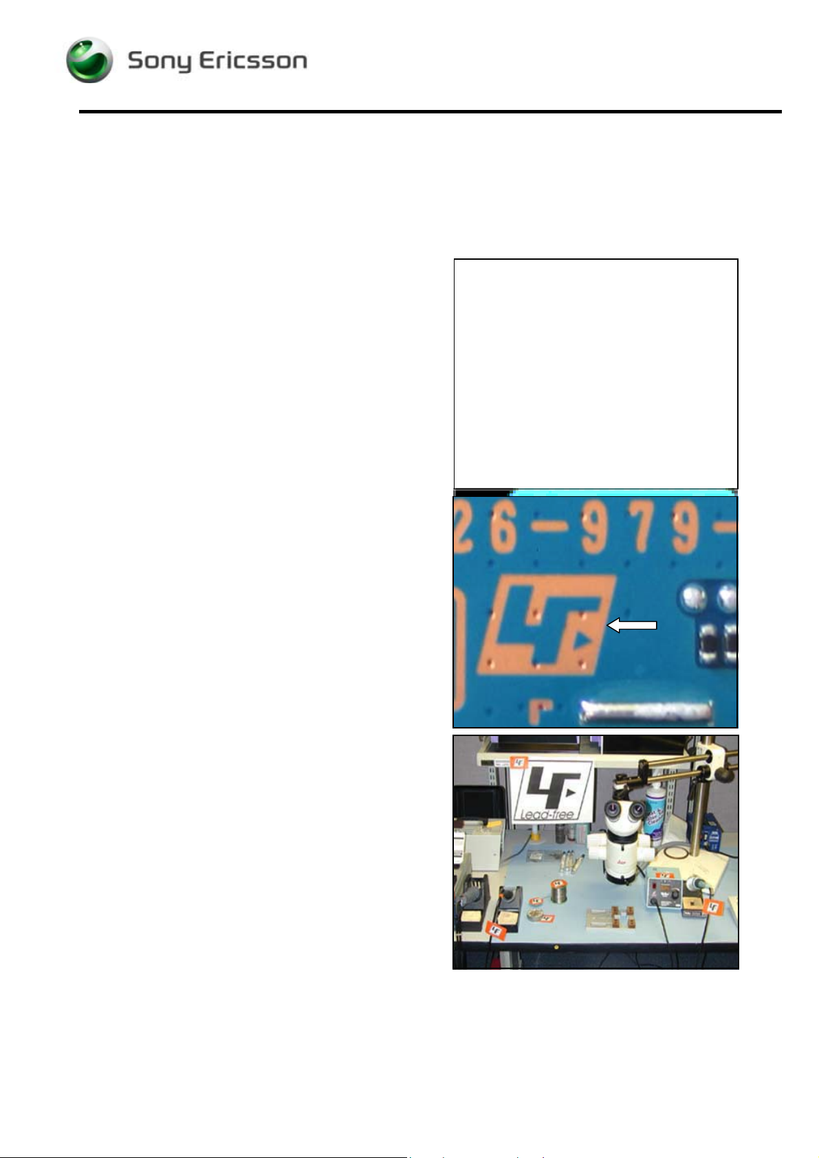
1 Lead-free soldering
Caution
Keep all contact surfaces clean of dirt and hand grease.
This product is manufactured with lead-free
solder and lead-free components!
During electrical repair, it is critical to make sure
that no lead is introduced.
This symbol indicates that the product is leadfree.
All lead-free PBA’s will be marked with this
symbol.
A lead-free work area must be set up completely
separated from work areas that are used to make
lead repairs.
The lead-free work area must also be clearly
labeled with the lead free symbol as shown in the
adjacent picture.
The items on this desk must remain lead-free.
They must be adequately labeled to make their
lead-free status clearly and easily recognized.
3/00021-2/FEA 209 544/94 C
Company Internal
©
Sony Ericsson Mobile Communicat i ons AB
3(23)
Page 4
K750 Working Instructions - electrical
LFS (lead-free solder paste) characteristics:
• High melting point (typically 220°C)
• Low wettability
• High surface tension
• Difficult to spread
• Recommended tip temperature = 370°C
When servicing PBA’s that have been
manufactured with LFS (lead-free solder paste),
LFS must
If not, there is a high risk for unreliable
soldering joints.
be used.
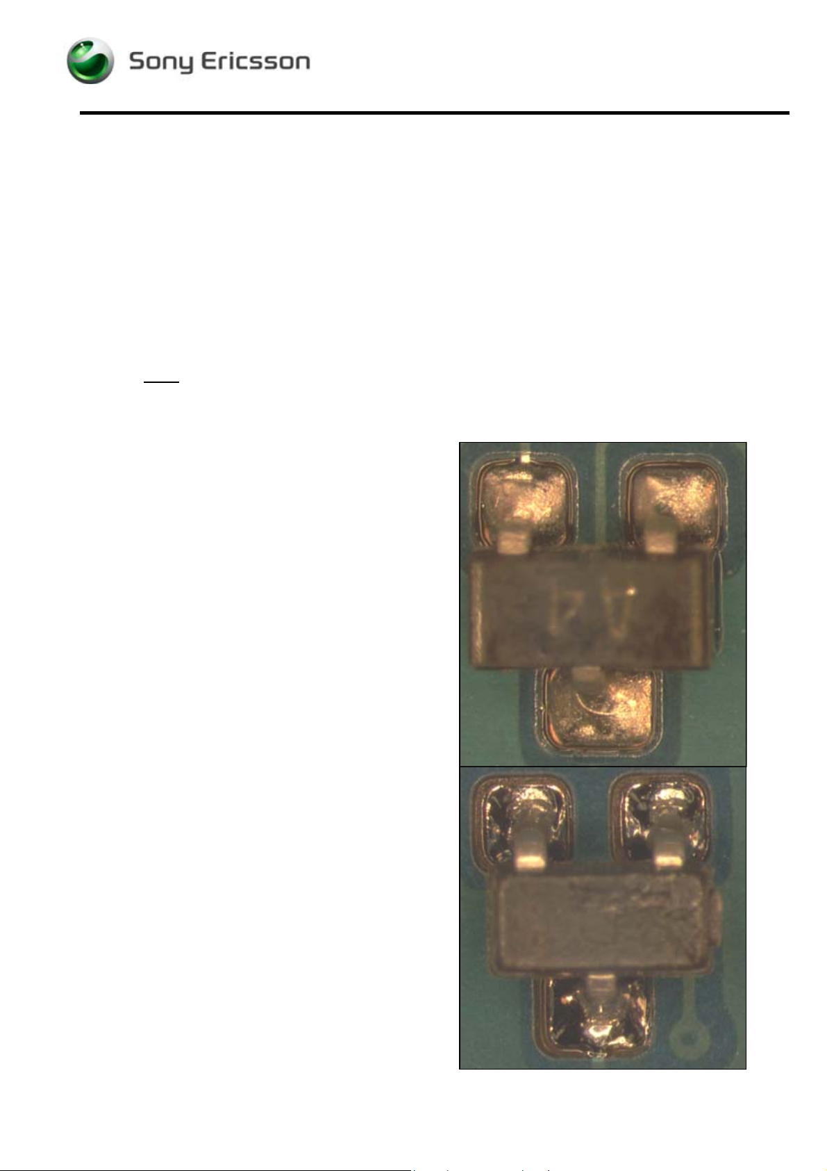
Lead-free solder joints are more difficult to
inspect because they do not have shiny surfaces
like leaded solder joints.
Also, lead-free solder does not flow as well as
leaded solder, so some of the solder pad areas
may remain exposed.
Example of lead-free solder joints.
Example of solder joints with lead.
3/00021-2/FEA 209 544/94 C
Company Internal
©
Sony Ericsson Mobile Communicat i ons AB
4(23)
Page 5
K750 Working Instructions - electrical
Example of lead-free solder joints.
Example of solder joints with lead.
3/00021-2/FEA 209 544/94 C
Company Internal
©
Sony Ericsson Mobile Communicat i ons AB
5(23)
Page 6

K750 Working Instructions - electrical
2 BGA equipment reflow profiles
2.1 General
This document contains reflow profile recommendations for mobile phones and
similar products.
They are just general recommendations and considerations have to be taken for
every single product.
The solder paste is secondary but could also affect the parameters.
In this document one alloy is specified:
SnAgCu (Lead free) melting point 217°C
2.2 Temperature measurement
At least 4 probes should be used.
They should be placed on components with the highest and lowest thermal mass.
The probes shall be located in the beginning, in the middle and at the end of the
board/panel.
It is recommended that the probes are soldered on the board, but glue and capton
tape could also be used, if necessary.
At least one probe shall be placed in the air or on top of a component.
These values are strongly depending on the BGA replacement equipment.
Nozzle type will be chosen after the outer size of the actual component.
Make sure the nozzle does not affect any nearby placed components.
These values are recommendations and may have to be changed depending on the
type of equipment.
The maximum temperature for any component must not exceed 250
°C.
3/00021-2/FEA 209 544/94 C
Company Internal
©
Sony Ericsson Mobile Communicat i ons AB
6(23)
Page 7
K750 Working Instructions - electrical
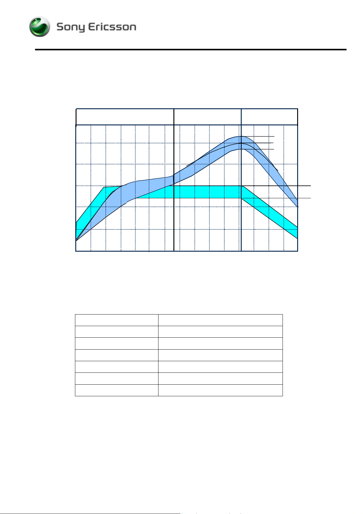
2.3 Reflow profiles
Sn/Ag/Cu (lead-free)
290
250
Preheat zone
Reflow zone
Cooling zone
260°C
245°C
235°C
200
150
Temperature [ºC]
100
150°C
125°C
50
0
40 80 120 160 200 240 280
Time [Seconds]
Ramp rate < 4°C/sec
Ramp rate cooling zone < 6°C/sec
Time above liquidus 60-150 sec
Minimum temperature 235°C
Maximum temperature 245°C or 260°C* for 10 sec
Bottom heat temperature 125°C-150°C
Total time Appr. 4-7 min
* The higher temperature in case the board has extremely high ∆T.
3/00021-2/FEA 209 544/94 C
Company Internal
©
Sony Ericsson Mobile Communicat i ons AB
7(23)
Page 8

K750 Working Instructions - electrical
3 Replacement of parts
Equipment
• Dentist hook
• ESD-gloves (cotton gloves)
• ESD-wristband
• Soldering tool
• Hot air soldering station
• BGA replacement equipment
• Pair of tweezers
• Solder cleaning wiper (tin wick)
• Solder paste lead-free (SN 96% Ag 3.5% Cu 0.5%)
Use the soldering tip only for lead-free solder paste!
• Flux, RMA no-clean flux
• Cutting pliers
• Shield fence pliers NTZ 112 537
Caution
Keep all contact surfaces clean of dirt and hand-grease
Instruction
For all the following part replacements, disassemble and assemble the phone as
described in Working Instructions 3/200021-1/FEA 209 544/94.
3/00021-2/FEA 209 544/94 C
Company Internal
©
Sony Ericsson Mobile Communicat i ons AB
8(23)
Page 9

K750 Working Instructions - electrical
3.1 Backup capacitor
Do not use hot air soldering equipment since the
nearby switch is heat sensitive!
Replace the backup capacitor using a soldering
iron.
3.2 External antenna switch
Replace the external antenna switch.
Use hot air soldering equipment to remove the
switch.
Use BGA repair equipment to resolder the new
switch.
3/00021-2/FEA 209 544/94 C
Company Internal
©
Sony Ericsson Mobile Communicat i ons AB
9(23)
Page 10

K750 Working Instructions - electrical
3.3 Camera connector BtB 30 pin
Replace the camera connector.
Use hot air equipment to remove the connector.
Use a soldering iron to mount the connector.
3/00021-2/FEA 209 544/94 C
Company Internal
©
Sony Ericsson Mobile Communicat i ons AB
10(23)
Page 11

K750 Working Instructions - electrical
3.4 LCD connector BtB 20 pin
Replace the LCD connector.
Use hot air equipment to remove the connector.
Use a soldering iron to mount the connector.
3/00021-2/FEA 209 544/94 C
Company Internal
©
Sony Ericsson Mobile Communicat i ons AB
11(23)
Page 12

K750 Working Instructions - electrical
3.5 Keyboard connector BtB 20 pin
Replace the keyboard connector.
Use hot air equipment to remove the connector.
Use a soldering iron to mount the connector.
3/00021-2/FEA 209 544/94 C
Company Internal
©
Sony Ericsson Mobile Communicat i ons AB
12(23)
Page 13

K750 Working Instructions - electrical
3.6 SIM reader
Use BGA repair equipment to remove and
replace the SIM reader.
3.7 Battery connector
Use BGA repair equipment to remove and replace
the battery connector.
3/00021-2/FEA 209 544/94 C
Company Internal
©
Sony Ericsson Mobile Communicat i ons AB
13(23)
Page 14

K750 Working Instructions - electrical
3.8 Memory stick Duo reader
Remove and replace the memory stick reader.
Use a soldering iron.
3.9 IrDA
Remove and replace the IrDA component.
Use a soldering iron or hot air soldering
equipment.
3/00021-2/FEA 209 544/94 C
Company Internal
©
Sony Ericsson Mobile Communicat i ons AB
14(23)
Page 15

K750 Working Instructions - electrical
3.10 Joystick switch
Use BGA repair equipment to remove and
replace the joystick switch.
3.11 Side key switch
Remove the side key switch.
Use hot air soldering equipment.
Assemble a new side key switch.
Use a soldering iron.
3/00021-2/FEA 209 544/94 C
Company Internal
©
Sony Ericsson Mobile Communicat i ons AB
15(23)
Page 16

K750 Working Instructions - electrical
3.12 Microphone
Remove and replace the microphone.
Use BGA repair equipment.
3/00021-2/FEA 209 544/94 C
Company Internal
©
Sony Ericsson Mobile Communicat i ons AB
16(23)
Page 17

K750 Working Instructions - electrical
3.13 Red LED
Remove and replace the red LED.
Use soldering iron equipment.
3/00021-2/FEA 209 544/94 C
Company Internal
©
Sony Ericsson Mobile Communicat i ons AB
17(23)
Page 18

K750 Working Instructions - electrical
3.14 Diode/ESD protector
Remove and replace the diode/ESD protector
component.
Use BGA repair equipment.
3/00021-2/FEA 209 544/94 C
Company Internal
©
Sony Ericsson Mobile Communicat i ons AB
18(23)
Page 19

K750 Working Instructions - electrical
3.15 Quartz crystal unit
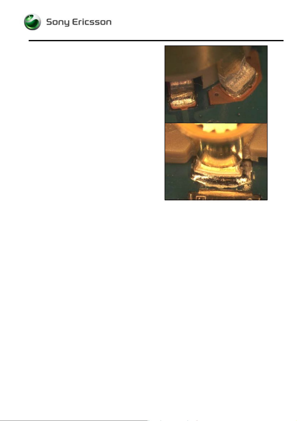
Remove the shield can lid.
If needed, it is allowed to remove the pick-up area
with cutting pliers.
This pick-up area is only used when the can is
machine mounted and there is no need to put it
back.
Cut the fence according to the white lines in the
picture.
Make sure that the cutting pliers are sharp-
edged to prevent damages to the shield can
fence!
Replace the quartz crystal component.
Use a soldering iron.
Put back a new shield can lid.
Press on all sides of the lid until you hear a “click”
sound.
3/00021-2/FEA 209 544/94 C
Company Internal
©
Sony Ericsson Mobile Communicat i ons AB
19(23)
Page 20

K750 Working Instructions - electrical
3.16 Prod adapt circuit/ASIC Tjatte 2
Remove the shield can lid.
Cut the fence according to the white line in the
picture.
Make sure that the cutting pliers are sharp-
edged to prevent damages to the shield can
fence!
Form the frame carefully without bending the
shield can fence wall.
Use the shield fence pliers.
Remove the the ASIC Tjatte 2 component.
Use BGA repair equipment.
Replace the ASIC Tjatte 2 component and gently
fold back the fence.
Be very cautious with the shield can fence wall.
3/00021-2/FEA 209 544/94 C
Company Internal
©
Sony Ericsson Mobile Communicat i ons AB
20(23)
Page 21

K750 Working Instructions - electrical
Gently fold back the fence.
Be very cautious with the shield can fence wall.
Put back a new
shield can lid.
Press on all sides of the lid until you hear a “click”
sound.
3.17 Prod adapt circuit/ASIC Vincenne
Remove the shield can lid.
Remove the ASIC Vincenne component.
Use BGA repair equipment.
Replace the ASIC Vincenne component.
Use BGA repair equipment.
3/00021-2/FEA 209 544/94 C
Company Internal
©
Sony Ericsson Mobile Communicat i ons AB
21(23)
Page 22

K750 Working Instructions - electrical
3.18 Mini T-top
To be added later
3/00021-2/FEA 209 544/94 C
Company Internal
©
Sony Ericsson Mobile Communicat i ons AB
22(23)
Page 23

K750 Working Instructions - electrical
4 Revision History
Rev. Date Changes / Comments
A 2005-05-13 Initial release
B 2005-05-19 Due to system problem
C 2005-05-19 Due to system problem
3/00021-2/FEA 209 544/94 C
Company Internal
©
Sony Ericsson Mobile Communicat i ons AB
23(23)
 Loading...