

Page 1
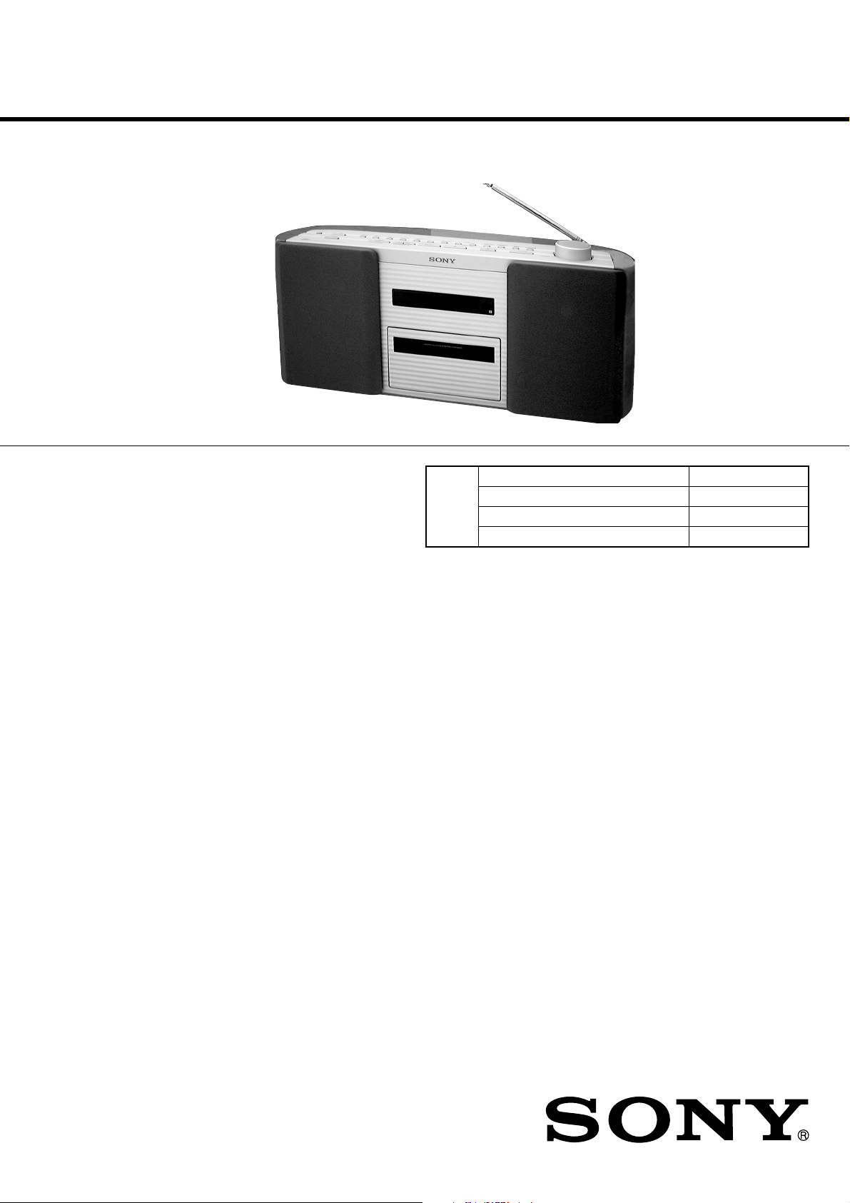
ZS-2000
SERVICE MANUAL
Ver 1.0 2000. 07
AUDIO POWER SPECIFICATIONS
POWER OUTPUT AND TOTAL
HARMONIC DISTORTION
With 4-ohm loads, both channels driven from
150 - 15,000 Hz; rated 6.5 W per channelminimum RMS power, with no more than 10%
total harmonic distortion in AC operation.
CD
Section
SPECIFICATIONS
US Model
Model Name Using Similar Mechanism ZS-D50
CD Loading Mechanism Type VLM-ZS2000
CD Mechanism Type CDM-2411AAA
Optical Pick-up Name DAX-01A2
CD player section
System
Compact disc digital audio system
Laser diode properties
Material: GaAlAs
Wave length: 780 nm
Emission duration: Continuous
Laser output: Less than 44.6 µW
(This output is the value measured at a distance of
about 200 mm from the objective lens surface on
the optical pick-up block with 7 mm aperture.)
Spindle speed
200 r/min (rpm) to 500 r/min (rpm) (CLV)
Number of channels
2
Frequency response
20 - 20,000 Hz +0.5/–0.7 dB
Wow and flutter
Below measurable limit
Radio section
Frequency range
FM: 87.6 - 108 MHz
AM: 530 - 1,710 kHz
Antennas
FM: Telescopic antenna
AM: Loop antenna
General
Speaker
Full range: 8 cm (3
Input
LINE IN jack (stereo minijack)
Minimum input level 250 mV
Outputs
Headphones jack (stereo minijack)
For 16 - 68 ohms impedance headphones
OPTICAL DIGITAL OUT (CD) (optical output
connector)
W avelength: 630 - 690 nm
Power requirements
For personal audio system:
120 V AC, 60 Hz
For remote control:
3 V DC, 2 size AA (R6) batteries
Power consumption
AC 30 W
Dimensions (incl. projecting parts)
approx. 470 × 206.5 × 145.5 mm (w/h/d)
5
/8 × 8 1/4 × 5 3/4 inches)
(18
Mass
approx. 5 kg (11 lb.)
Supplied accessories
Remote control (RMT-C200A) (1)
AM loop antenna (1)
Speaker nets (2)
Design and specifications are subject to change without
notice.
1
/4 in.) dia., 4 ohms, cone type x 2
– 1 –
PERSONAL AUDIO SYSTEM
Page 2

TABLE OF CONTENTS
1. SERVICING NOTES
1-1. Laser Diode and Focus Search Operation Check................ 4
1-2. Caution During when Mounting the Pulley for the
Loading Motor .................................................................... 4
2. GENERAL
Playing a CD ....................................................................... 5
Listening to the radio........................................................... 5
Setting the clock .................................................................. 6
Setting the time signal ......................................................... 6
Saving Power....................................................................... 6
3. DISASSEMBLY
3-1. “Net Sub Assy, Saran”, Speaker (Front) Sub Assy ............. 7
3-2. Cabinet, Front...................................................................... 8
3-3. Top Cabinet Assy ................................................................ 9
3-4. CD Block Assy.................................................................... 9
3-5. Power Board, REG Board .................................................10
3-6. TU Board........................................................................... 10
3-7. “Cover, Heat Sink”, Line Board........................................11
3-8. Volume Board ....................................................................11
3-9. H/P Board, Switch (1) Board, Switch (2) Board............... 12
3-10. FL Board ........................................................................... 12
3-11. Control Board, Lamp Board.............................................. 13
3-12. Main Board ....................................................................... 13
3-13. CD Board ..........................................................................14
3-14. CD Block Section.............................................................. 14
3-15. Tray Assy, CD ................................................................... 15
3-16. Loading Board................................................................... 15
3-17. Optical Pick-up Block, Pick-up Relay Board ................... 16
4. TEST MODE
4-1. General Description ..........................................................17
4-2. Test Mode .......................................................................... 17
5. ELECTRICAL ADJUSTMENTS
5-1. Tuner Section .................................................................... 18
5-2. CD Section ........................................................................ 19
6. DIAGRAMS
6-1. IC Pin Description............................................................. 20
6-2. Circuit Boards Location ....................................................22
6-3. Block Diagram –Tuner Section–....................................... 23
6-4. Block Diagram –CD Section–........................................... 25
6-5. Block Diagram –Audio Section– ...................................... 27
6-6. Printed Wiring Board –Tuner Section– ............................. 29
6-7. Schematic Diagram –Tuner Section–................................31
6-8. Printed Wiring Board –CD Section– ................................. 33
6-9. Schematic Diagrams –CD Section– .................................. 35
6-10. Printed Wiring Boards –Pick-up Section– ........................ 37
6-11. Schematic Diagrams –Pick-up Section– ...........................39
6-12. Printed Wiring Boards –Main Section– ............................ 41
6-13. Schematic Diagrams –Main Section– ...............................43
6-14. Printed Wiring Boards –Control Section–......................... 45
6-15. Schematic Diagrams –Control Section– ........................... 47
6-16. Printed Wiring Boards –Display Section– ........................ 49
6-17. Schematic Diagrams –Display Section– ...........................51
6-18. Printed Wiring Boards –Power Supply Section– .............. 53
6-19. Schematic Diagrams –Power Supply Section– .................55
7. EXPLODED VIEWS
7-1. Front Cabinet Section........................................................ 60
7-2. Rear Cabinet Section......................................................... 61
7-3. CD Block Section.............................................................. 62
7-4. CD Loading Section (VLM-ZS2000) ............................... 63
7-5. Optical Pick-up Section (CDM-2411AA) .........................64
8. ELECTRICAL PARTS LIST......................................65
– 2 –
Page 3
CAUTION
Use of controls or adjustments or performance of procedures other than those specified herein may result in hazardous radiation exposure.
NOTES ON HANDLING THE OPTICAL PICK-UP
BLOCK OR BASE UNIT
The laser diode in the optical pick-up block may suffer electrostatic break-down because of the potential difference generated
by the charged electrostatic load, etc. on clothing and the human
body.
During repair, pay attention to electrostatic break-down and also
use the procedure in the printed matter which is included in the
repair parts.
The flexible board is easily damaged and should be handled with
care.
NOTES ON LASER DIODE EMISSION CHECK
The laser beam on this model is concentrated so as to be focused
on the disc reflective surface by the objective lens in the optical
pick-up block. Therefore, when checking the laser diode emission, observe from more than 30 cm away from the objective lens.
NOTES ON CHIP COMPONENT REPLACEMENT
• Never reuse a disconnected chip component.
• Notice that the minus side of a tantalum capacitor may be damaged by heat.
SAFETY CHECK-OUT
After correcting the original service problem, perform the following
safety check before releasing the set to the customer:
Check the antenna terminals, metal trim, “metallized” knobs, screws,
and all other exposed metal parts for AC leakage. Check leakage as
described below.
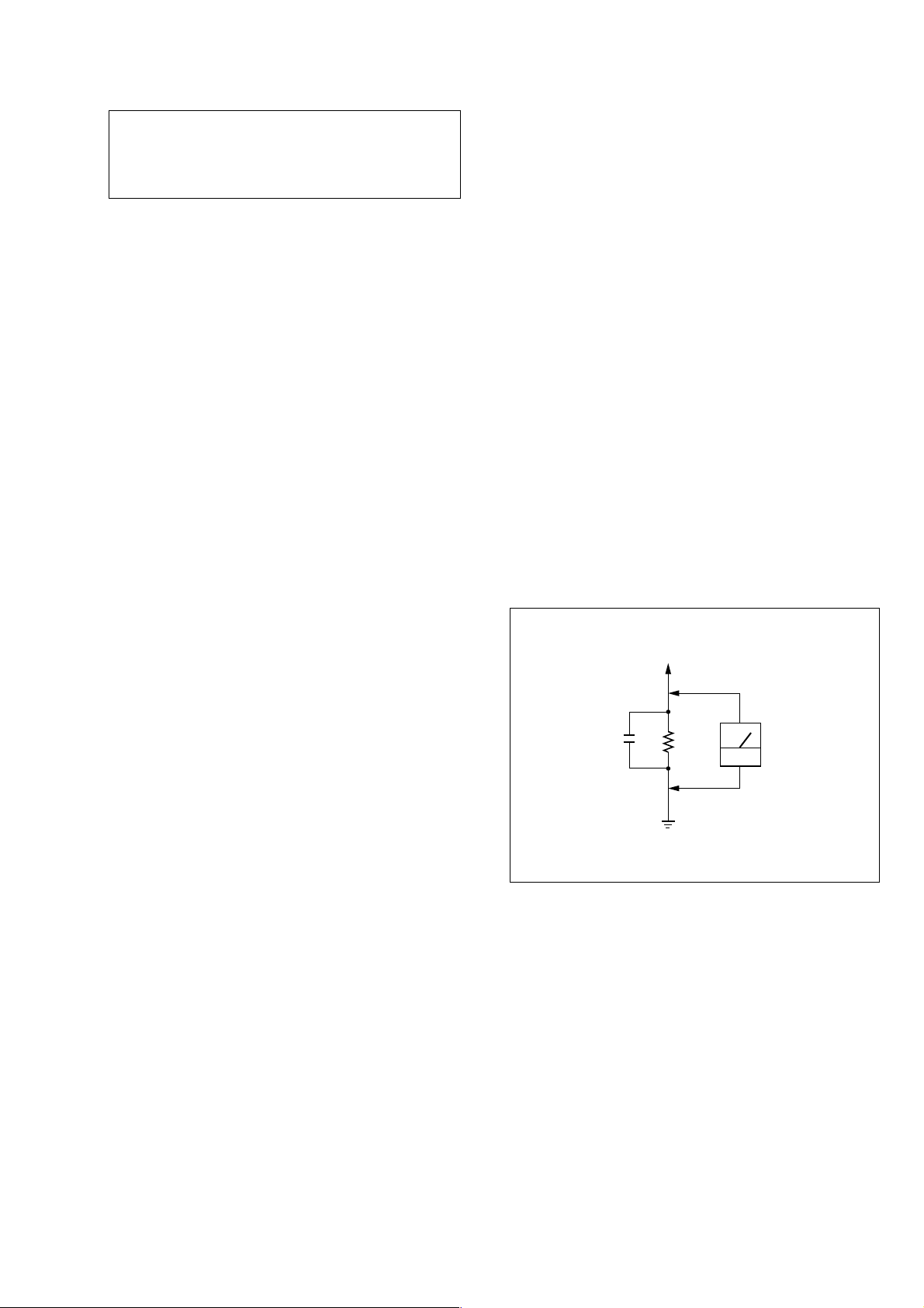
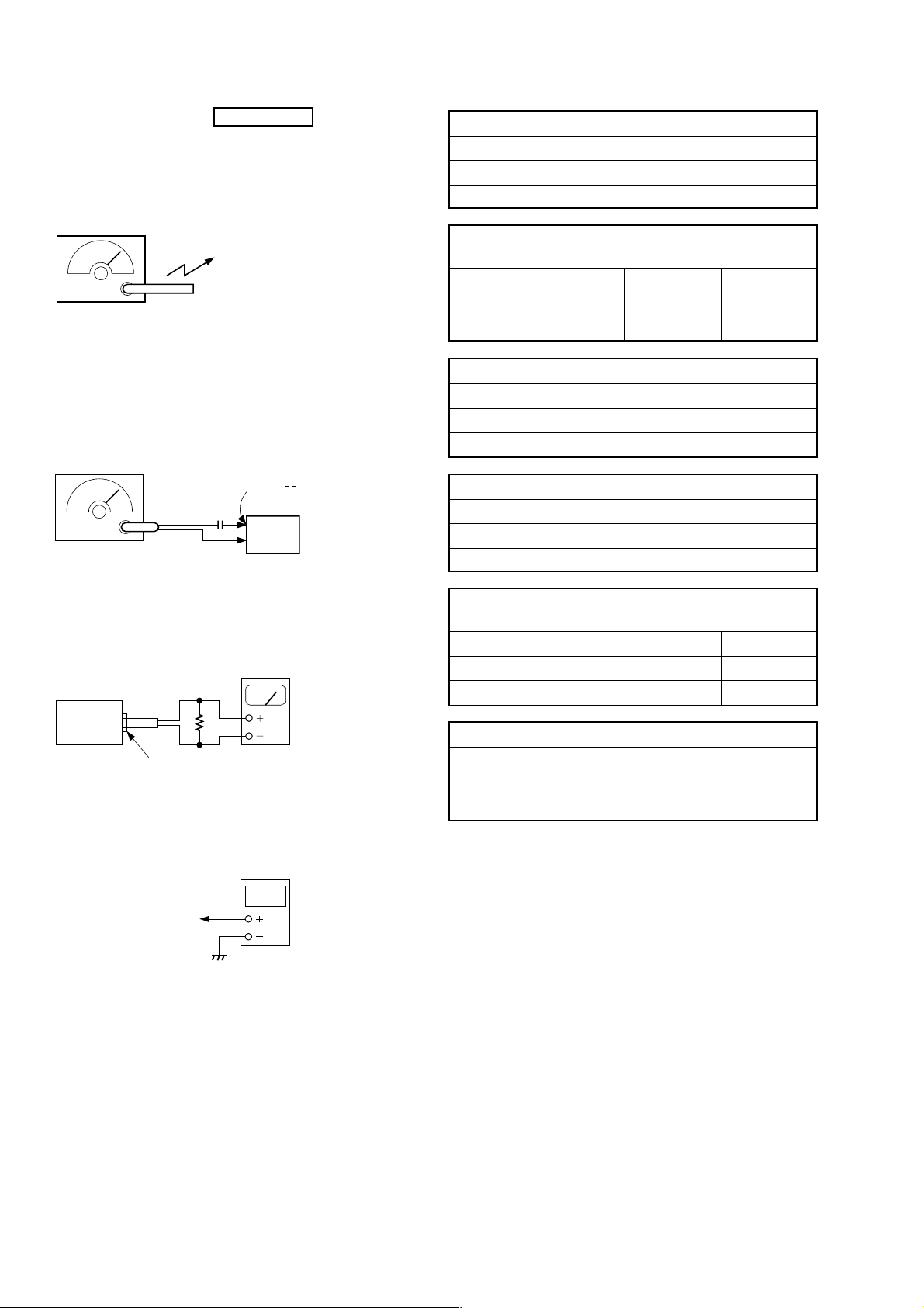
LEAKAGE TEST
The AC leakage from any exposed metal part to earth ground and
from all exposed metal parts to any exposed metal part having a
return to chassis, must not exceed 0.5 mA (500 microamperes).
Leakage current can be measured by any one of three methods.
1. A commercial leakage tester, such as the Simpson 229 or RCA
WT-540A. Follow the manufacturers’ instructions to use these
instruments.
2. A battery-operated AC milliammeter. The Data Precision 245
digital multimeter is suitable for this job.
3. Measuring the voltage drop across a resistor by means of a VOM
or battery-operated AC voltmeter . The “limit” indication is 0.75
V , so analog meters must have an accurate low-voltage scale. The
Simpson 250 and Sanwa SH-63Trd are examples of a passive
VOM that is suitable. Nearly all battery operated digital
multimeters that have a 2V AC range are suitable. (See Fig. A)
FLEXIBLE CIRCUIT BOARD REPAIRING
• Keep the temperature of the soldering iron around 270 ˚C during repairing.
• Do not touch the soldering iron on the same conductor of the
circuit board (within 3 times).
• Be careful not to apply force on the conductor when soldering
or unsoldering.
To Exposed Metal
Parts on Set
0.15µF
Ω
1.5k
Earth Ground
AC
voltmeter
(0.75V)
Fig. A. Using an AC voltmeter to check AC leakage.
SAFETY-RELATED COMPONENT WARNING!!
COMPONENTS IDENTIFIED BY MARK 0 OR DOTTED LINE
WITH MARK 0 ON THE SCHEMATIC DIAGRAMS AND IN
THE PARTS LIST ARE CRITICAL TO SAFE OPERATION.
REPLACE THESE COMPONENTS WITH SONY P AR TS WHOSE
PART NUMBERS APPEAR AS SHOWN IN THIS MANUAL
OR IN SUPPLEMENTS PUBLISHED BY SONY.
– 3 –
Page 4
SECTION 1
SERVICING NOTES
1-1. LASER DIODE AND FOCUS SEARCH
OPERATION CHECK
1. Close the lid for CD.
2. Press CD u button.
3. Confirm the laser diode emission while observing the objecting
lens. When there is no emission, Auto Power Control circuit or
Optical Pick-up is broken.
Objective lens moves up and down once for the focus search.
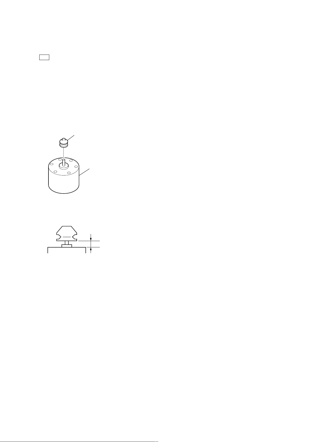
1-2. CAUTION DURING WHEN MOUNTING THE
PULLEY FOR THE LOADING MOTOR
Make the following adjustment when mounting the loading motor
(part number: 1-698-999-11) and motor pulley (part number: 2627-174-01) of the CD section.
pulley
M790
0.9 to 1.1 mm
Install the pulley to the motor.
– 4 –
Page 5
Basic Operations
SECTION 2
GENERAL
This section is extracted
from instruction manual.
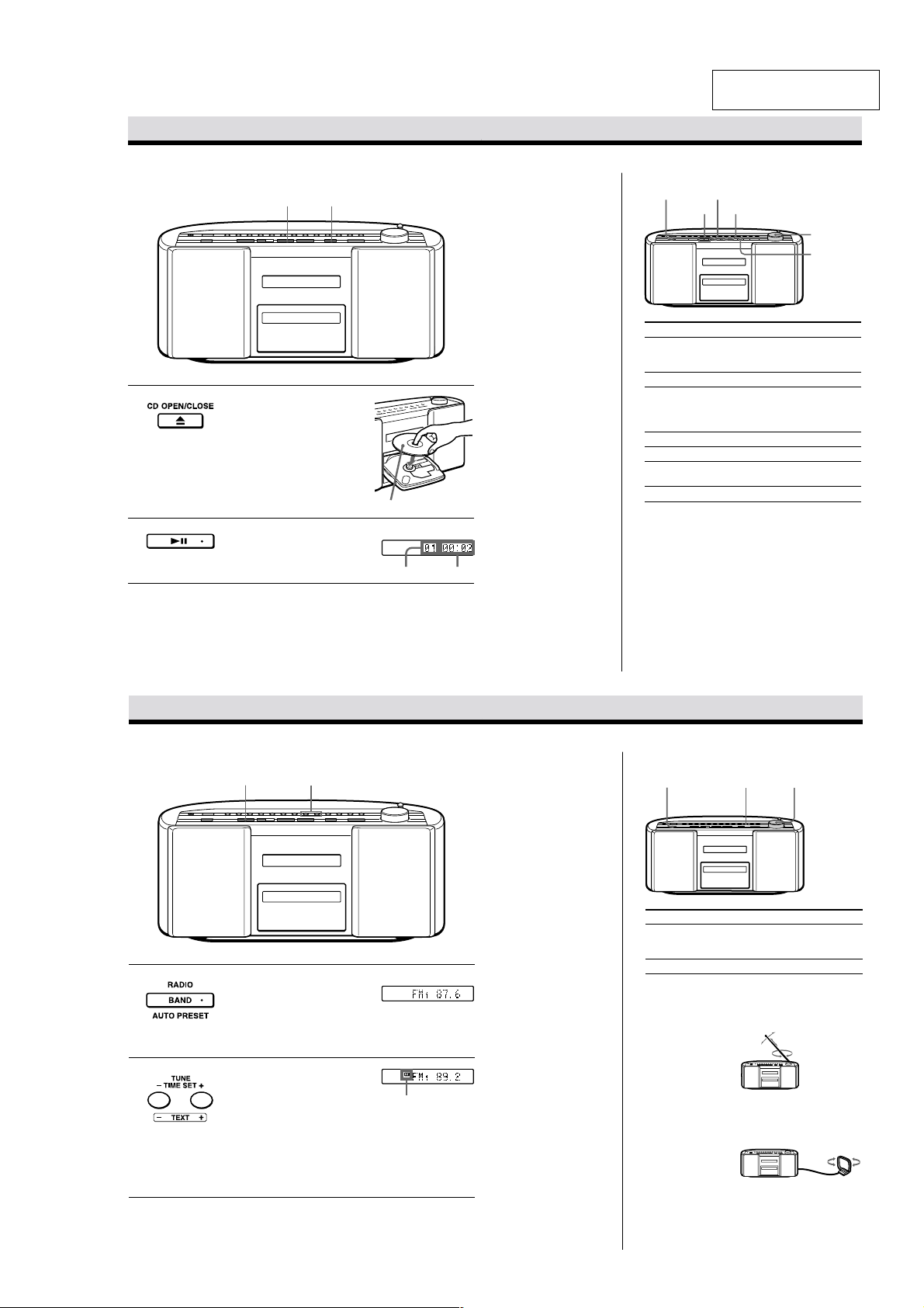
Playing a CD
1
2
Connect the AC power cord to the wall outlet (see page 26).
1 Press Z CD OPEN/CLOSE
(direct power-on) and place the
CD on the CD tray until it clicks
into place.
2 Press u (N on the remote).
The CD tray closes and the player
plays all the tracks once.
With the label side up
Display
Use these buttons for additional operations
., >
u
x
or – (press VOL +, – on
the remote).
remote).
Press again to resume play
after pause.
CLOSE.
VOLUME
CD
Z
OPEN/CLOSE
POWER
Tip
Next time you want to
listen to a CD, just press
u. The player turns on
automatically and starts
playing the CD.
Playing timeTrack number
To Do this
adjust the volume Turn VOLUME toward +
stop playback Press x.
pause playback Press u (X on the
go to the next track Press >.
go back to the previous track Press ..
remove the CD Press Z CD OPEN/
turn on/off the player Press POWER.
Listening to the radio
12
Connect the AC power cord to the wall outlet (see page 26).
1 Press RADIO BAND• AUTO
2 Hold down TUNE • TIME SET +
PRESET until the band you want
appears in the display (direct
power-on).
Each time you press the button,
the band changes as follows:
“FM1” t “FM2” t “AM”
or – (TUNE + or – on the remote)
until the frequency digits begin to
change in the display.
The player automatically scans
the radio frequencies and stops
when it finds a clear station.
If you cannot tune in a station,
press the button repeatedly to
change the frequency step by
step.
Display
Indicates an FM
stereo broadcast.
Tips
• The “FM1” and “FM2”
bands have the same
functions. You can store
the stations you want
separately in “FM1” and
“FM2” (page 14).
• If the FM broadcast is
noisy, press PLAY
MODE•MONO/ST
(MODE on the remote)
until “Mono ” appears in
the display and the
radio will play in
monaural.
• Next time you want to
listen to the radio, just
press RADIO BAND•
AUTO PRESET. The
player turns on
automatically and starts
playing the previous
station.
Use these buttons for additional operations
POWER
To Do this
adjust the volume Turn VOLUME toward +
turn on/off the radio Press POWER.
To improve broadcast reception
FM:
Reorient the antenna for FM.
AM:
Keep the AM loop antenna as far as possible from the
player and reorient it.
If the broadcast is still noisy, connect the external
antenna (page 27).
PLAY MODE
MONO/ST
VOLUME
or – (press VOL +, – on
the remote).
– 5 –
Page 6
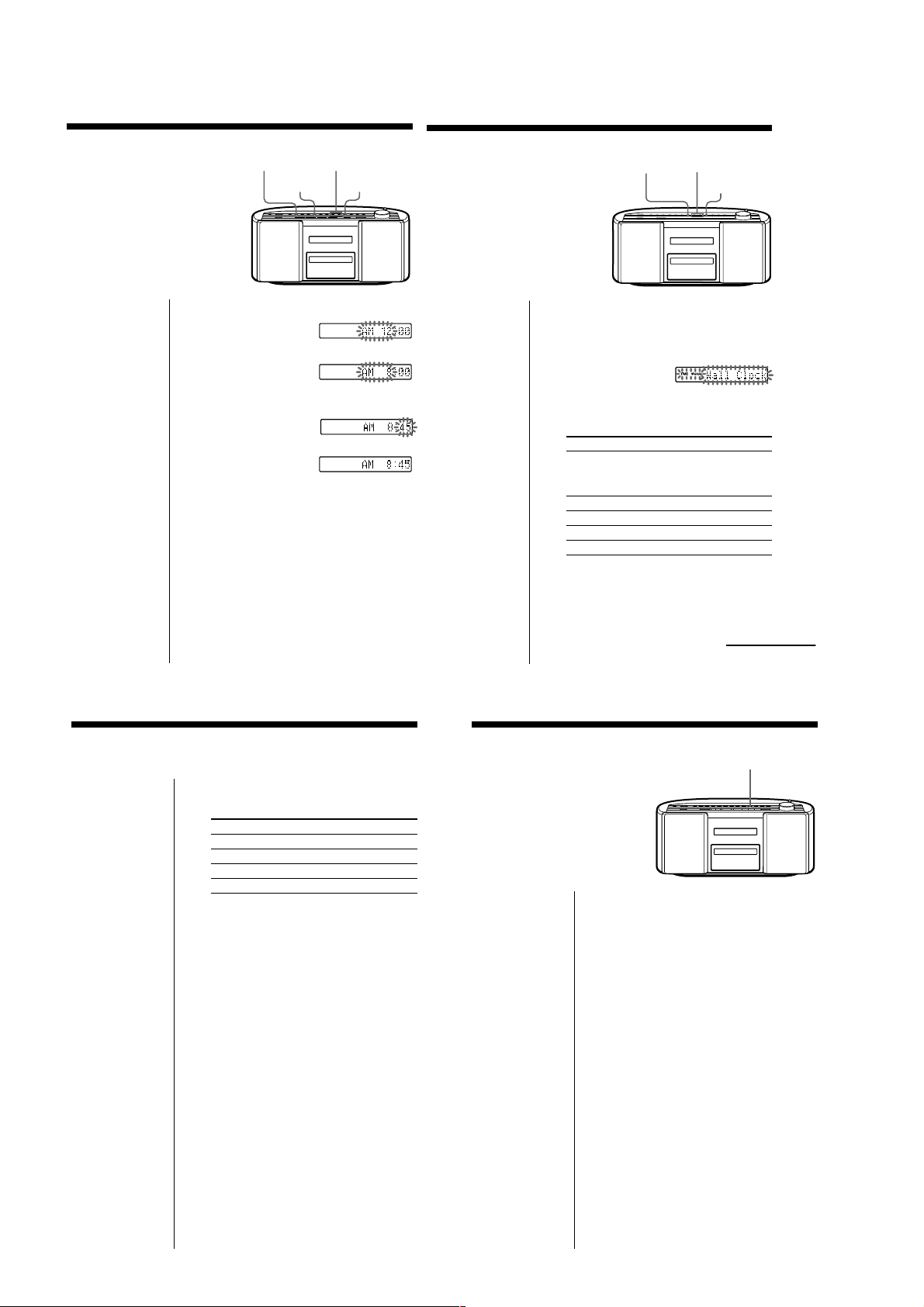
The Timer
Setting the clock
“– –:– –” indication appears in the
display until you set the clock.
Tip
The time display
system of this player is
the 12-hour system.
1
2
3
To change the display to the daylight saving time
(summer time) indication
Press and hold SUMMER TIME for 2 seconds.
“Summer On ” appears in the display for a few
seconds.
To cancel the summer time indication
Press and hold SUMMER TIME again.
“Summer Off” appears in the display for a few
seconds.
CLOCK
Press and hold CLOCK until the hour digits flash.
Set the time.
1 Press TUNE •TIME
SET + or – to set the
hour and press
• ENTER
DISPLAY
MEM.
2 Press TUNE •TIME
SET + or – to set the
minutes.
Press DISPLAY• ENTER
MEM.
The clock starts from 00
seconds.
TUNE
TIME SET –, +
SUMMER TIME
DISPLAY
ENTER MEM
m
Setting the time
signal
When the power is off, you can hear the
time signal on this player. You can select
the sound for the time signal. Make sure
you have set the clock (see page 18).
Note
The time signal does
not sound when the
player is turned on.
1
When the power is off, press TIME SIGNAL to
display “TIME SIGNAL ” indication.
Do the following operations by checking the
display.
2
Press TUNE • TIME SET + or – until the sound you
want appears in the display, and press DISPLAY•
ENTER MEM.
Display Intervals
Wall Clock Sounds on the hour the number of times
Harp Sounds on the hour once
Music Box Sounds on the hour once
Chime Sounds on the hour once
Organ Sounds on the hour once
3
Press TUNE • TIME SET + or – to set the volume
you want, and press DISPLAY• ENTER MEM.
TUNE
TIME SIGNAL
corresponding to the hour and again on the
half hour once (Example: Three times at
3:00 p.m. and again at 3:30 p.m. once).
TIME SET –, +
Display
DISPLAY
ENTER MEM
continued
Setting the time signal
(continued)
4 Press TUNE • TIME SET + or – to select the time for
the time signal function to work, and then press
DISPLAY• ENTER MEM.
Display Time signal sounds
Off Not at all
Every Hour All day
Auto 7:00 a.m. - 10:00 p.m.
Once a Day* Once a day
* If you selected “Wall Clock” in step 2, you cannot select
“Once a Day”
5 If you selected “Once a Day ” in step 4, set the time
for the time signal to sound. (If you selected other
items in step 4, omit this step.)
1 Press TUNE • TIME SET + or – to set the hour
and press DISPLAY• ENTER MEM.
2 Press TUNE • TIME SET + or – to set the minutes
and press DISPLAY• ENTER MEM.
To check the sound types (demonstration mode)
Press and hold TIME SIGNAL for about 2 seconds.
You can hear the five types of sound once.
Saving power
Even when power is turned off, this
player consumes about 5.6 W for time
indication, timer operation, remote
control reception. If you use the saving
power function, you can reduce power
consumption to less than 1 W.
When the power is off, press and hold
DISPLAY• ENTER MEM for about 2 seconds.
The player enters the lower power consumption
standby mode.
To cancel the saving power
To make the time indication appear, press and hold
DISPLAY• ENTER MEM for about 2 seconds when the
power is off.
DISPLAY
ENTER MEM
– 6 –
Page 7
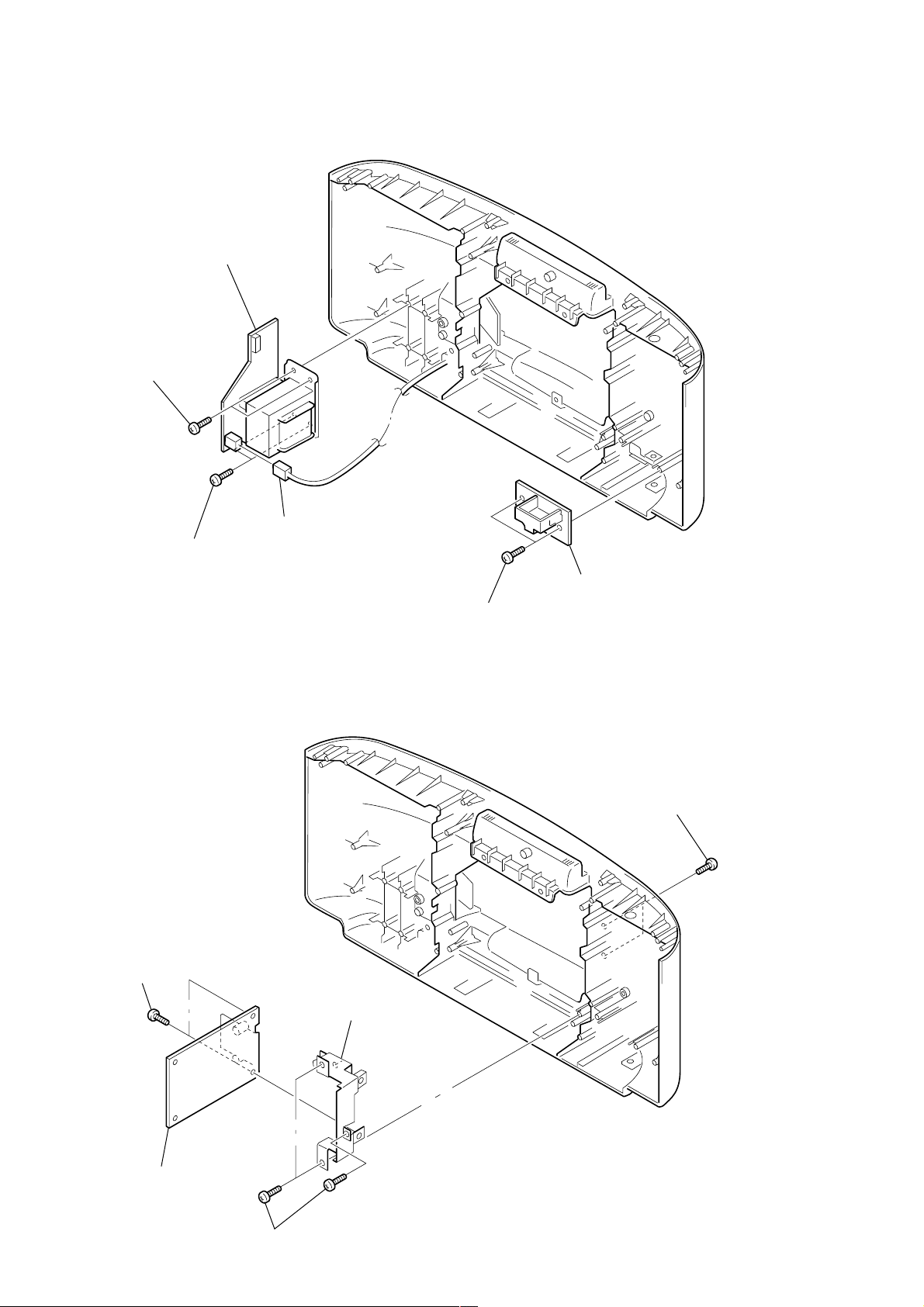
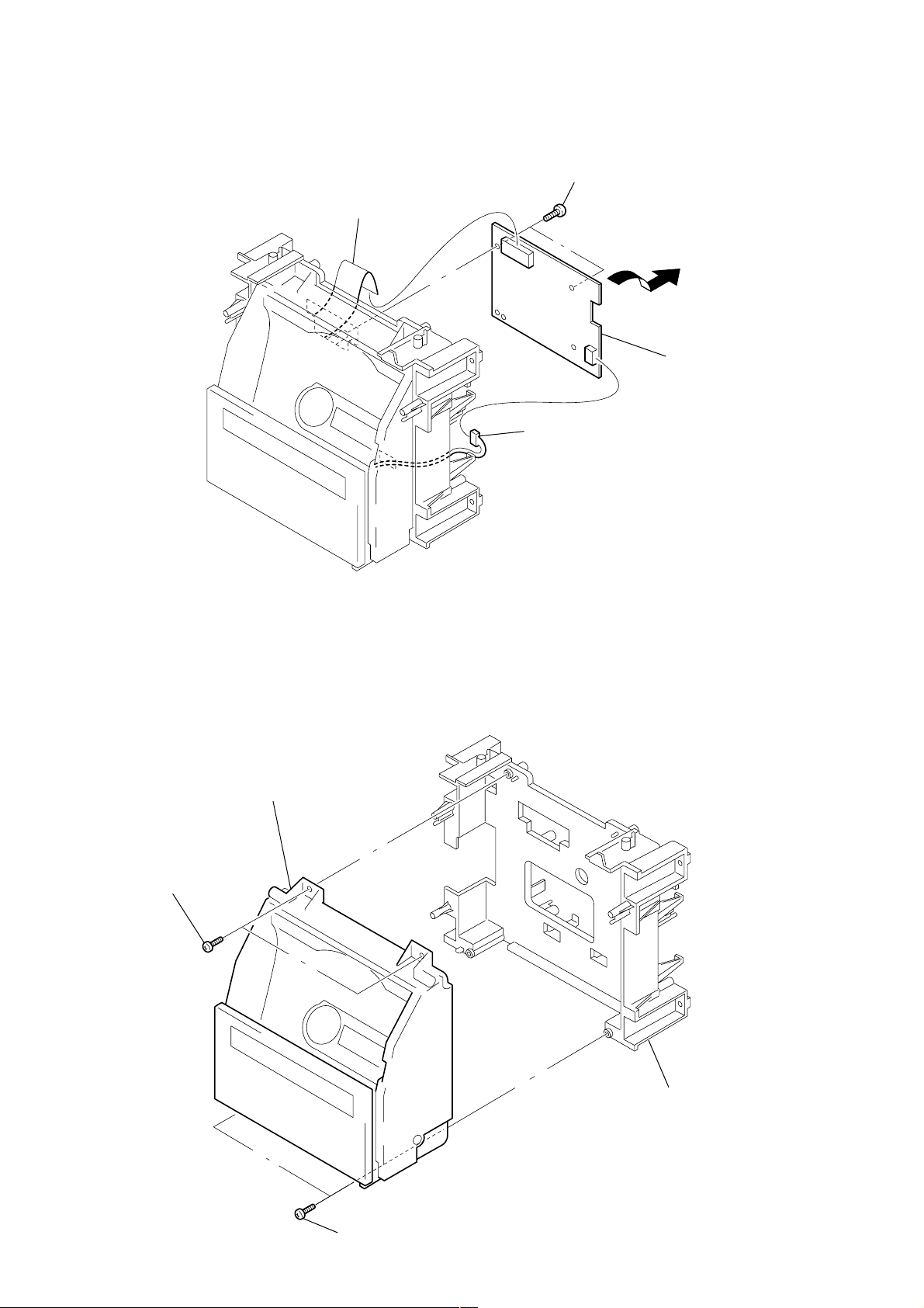
SECTION 3
)
y (R)
DISASSEMBLY
Note : This set can be disassemble according to the following sequence.
Set
“Net Sub Assy, Saran”, Speaker (Front) Sub Assy
Cabinet, Front
Power Board,
Top Cabinet Assy
Note : Follow the disassembly procedure in the numerical order given.
REG Board
Volume Board
H/P Board, Switch (1) Board,
Switch (2) Board
CD Block Assy
TU Board “Cover, Heat Sink”, Line Board
FL Board
Control Board, Lamp Board
Main Board CD Board CD Block Section
3-1. “NET SUB ASSY, SARAN”, SPEAKER (FRONT) SUB ASSY
7 CN304
6 speaker (front)
sub assy (L)
Tray Assy, CD
Loading Board
Optical Pick-up Block,
Pick-up Relay Board
4 BVTP 3x55
1 net sub assy (L), saran
2 BVTP 3x55
8 net sub ass
5 bush, net
3 bush, net
, saran
qs bush, net
qa BVTP 3x55
qf CN304
qd speaker (front) sub assy (R
0 bush, net
9 BVTP 3x55
– 7 –
Page 8
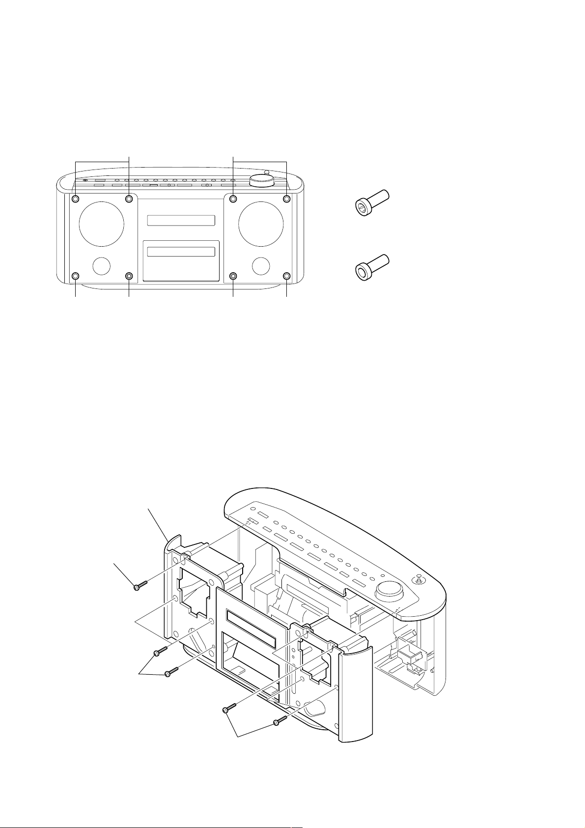
• Note for installation of the speaker (front) sub assy
y
B
AB
B
There are two types of net “bush, net”:
Type A: 3-041-456-11 (with groove in the tube)
Type B: 3-041-456-01 (without groove in the tube)
A B
The type A of “bush, net” should be installed at place A in the left figure.
pe B of “bush, net” should be installed at place B.
The t
3-2. CABINET, FRONT
3 BVTP 3x12
2 BVTP 3x12
4 cabinet, front
1 BVTP 3x12
– 8 –
Page 9
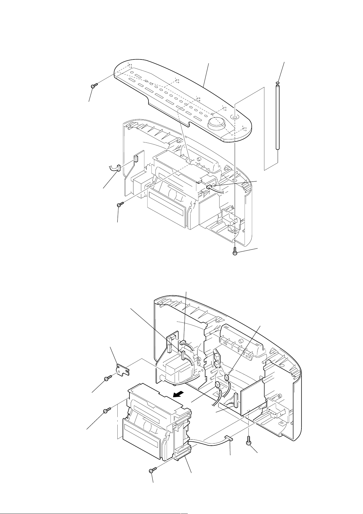
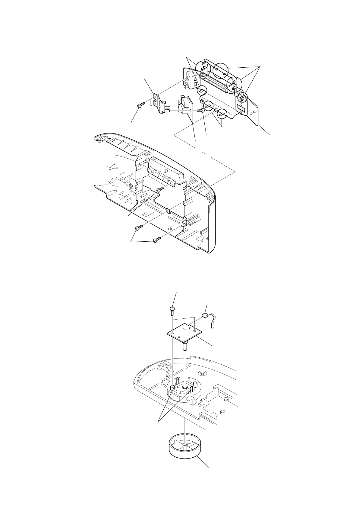
3-3. TOP CABINET ASSY
1 CN904
2 CN804
5 BVTP 3x10
6 BVTP 3x10
7 top cabinet assy
3 B 3x10
4 antenna, telescopic
3-4. CD BLOCK ASSY
5 RETAINER (2) board
4 BVTP 3x10
6 BVTP 3x10
2 CN902
7 BVTP 3x10
1 CN903
qa CN403
qs CNP1
qd Connector
9 CD block assy
3 CN310
0 CN402
8 BVTP 3x10
– 9 –
Page 10
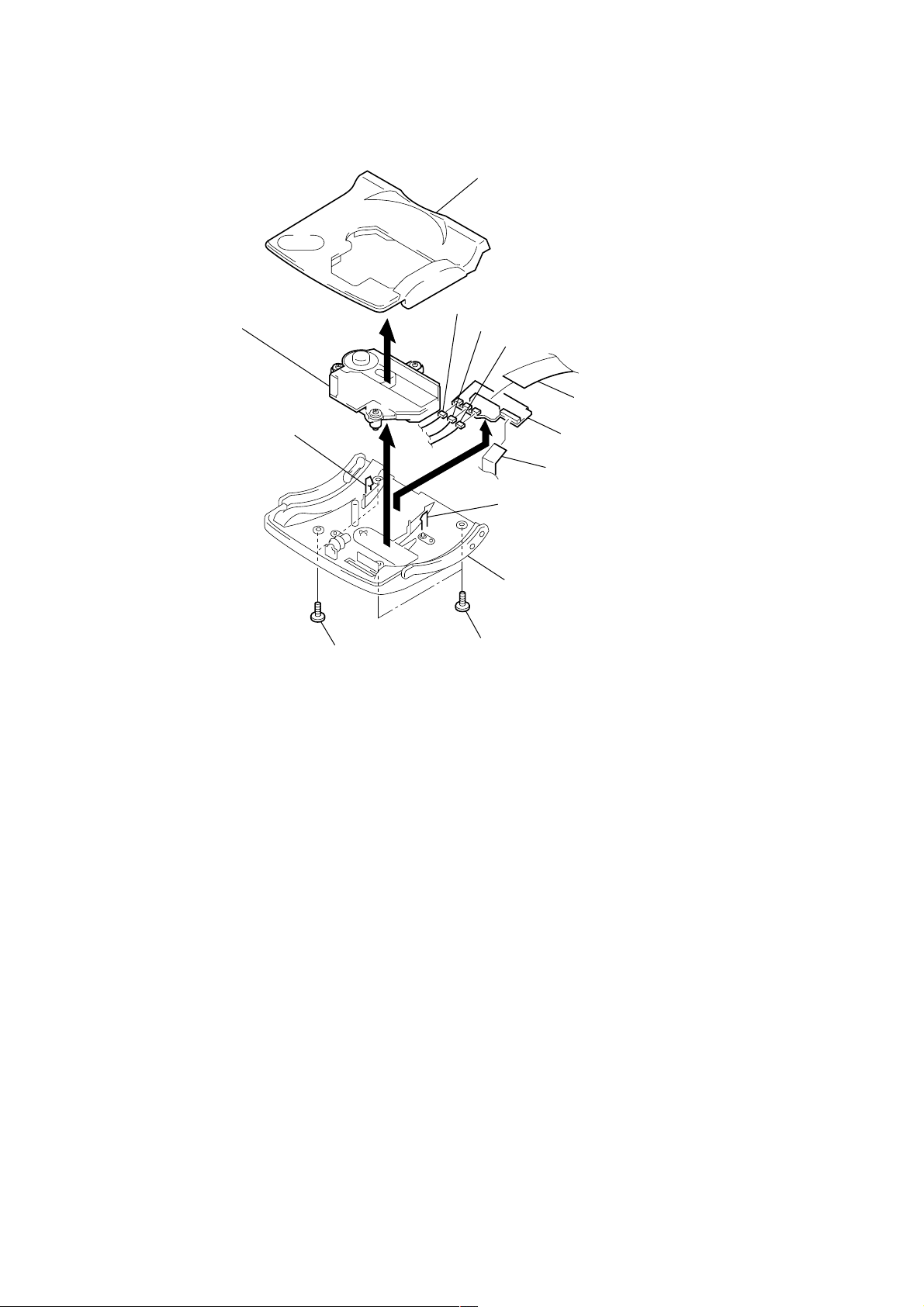
3-5. POWER BOARD, REG BOARD
4 POWER board
3 BVTP 3x10
1 CN901
2 BVTP 3x10
3-6. TU BO ARD
4 B 3x6
6 REG board
5 BVTP 3x10
1 BVTP 2.6x10
3 bracket, tuner
5 TU board
2 BVTP 3x10
– 10 –
Page 11
d
3-7. “COVER, HEAT SINK”, LINE BOARD
k
8 holder, line
5 claws
4 claws
2 BVTP 3x10
3-8. V OLUME BOARD
1 BVTP 3x10
7 BVTP 3x10
0 LINE board
3 BVTP 3x10
3 claws
9 BVTP 3x10
6 cover, heat sin
2 CN806
5 VOLUME boar
4 claws
1 knob (VOL)
– 11 –
Page 12
3-9. H/P BOARD, SWITCH (1) BOARD, SWITCH (2) BOARD
)
7 BVTP 3x8
9 SWITCH (1) board
8
6 BVTP 3x8
4 BVTP 3x8
5 SWITCH (2) board
3 CN805
1 PWH 2x8 (DIA.6
2 H/P board
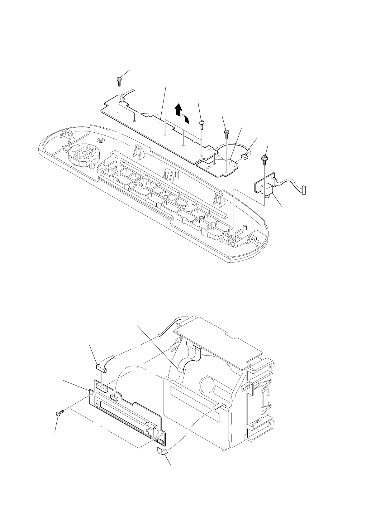
3-10. FL BOARD
4 FL board
3 BVTP 3x8
2 CN501
1 CN502
5 CN503
– 12 –
Page 13
3-11. CONTROL BOARD, LAMP BOARD
2 CN801
3 BVTP 3x10
4 CONTROL board
3-12. MAIN BOARD
5 LAMP board
claws
5 MAIN board
1 CN802
3 BVTP 3x10
4
– 13 –
2 BVTP 3x10
1 CN303
claws
Page 14
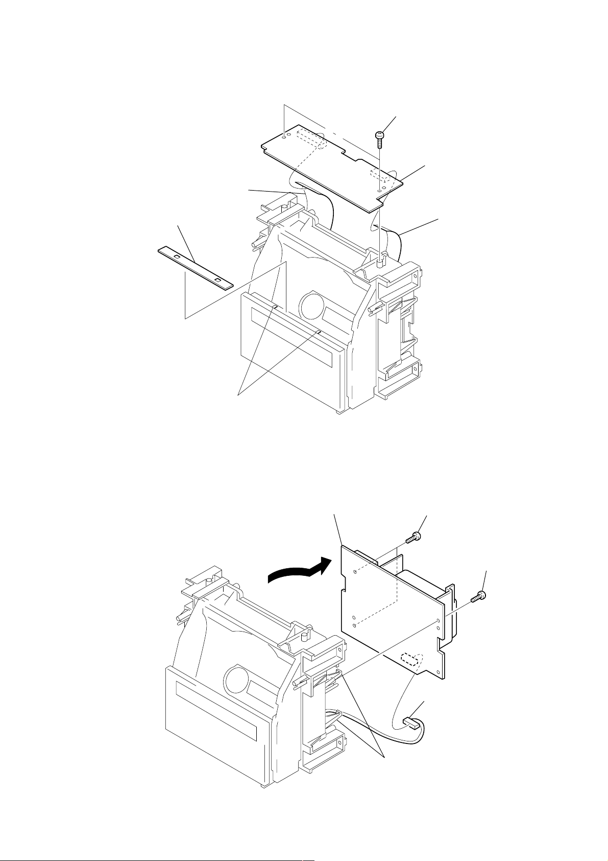
D
3-13. CD BOARD
d
2 BVTP 3x10
1 CN711
3
4 CD boar
5 CN713
3-14. CD BLOCK SECTION
1 BVTP 3x10
3 CD block section
chassis, C
2 BVTP 3x10
– 14 –
Page 15
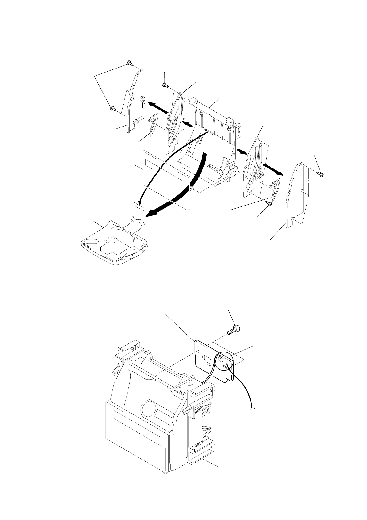
3-15. TRAY ASSY, CD
3 screws
(+BV 3x10)
4 cover (L), side
qf tray assy, CD
8 slider (L)
qa CD lid assy
qs
9 screws (+BV 3x10)
0 plate (L), side
qd
5 slider (R)
chassis, loading
7 plate (R), side
1 screws
(+BV 3x10)
6 screws
(+BV 3x10)
2 cover (R), side
3-16. LOADING BOARD
2 LOADING board
1 BVTP 3x10
3 Removal the solders.
– 15 –
CD block section
Page 16
3-17. OPTICAL PICK-UP BLOCK, PICK-UP RELAY BOARD
d
qa CN703
qs optical pick-up block
3 tray (top), CD
0 CN704
9 CN702
7 CN707
5 claw
2 BTP 2.6x8
6 PICK-UP RELAY boar
8 CN706
4 claw
tray (bottom), CD
1 BTP 2.6x8
– 16 –
Page 17
SLEEP
CLOCK TIMER
RADIO/BAND
AUTO PRESET
TEST-A
– SWITCH (1) BOARD –
SECTION 4
TEST MODE
4-1. GENERAL DESCRIPTION
This set has the TEST MODE that allows the CD unit to be
operational checked.
4-2. TEST MODE
4-2-1. Setting the test mode
1) Turn the power on.
2) Short the TEST-A land on the SWITCH(1) BOARD to open it
(or short between JW824 and JW825 to open the circuit).
4-2-2. Releasing the test mode
After the test mode is complete, turn the power off to release the
mode.
Display
88 x x xx
LCD display
(test item)
4-2-3. The contents of test mode
Mode name Description LCD display
STOP 1 The initial state and command are reset and the initial value is set.
After resetting, Stop 2 is switched to.
STOP 2 Stopped state.
FF/FR KEYis used to operate the SLED(PICK-UP).
The automatic adjustment value is held.
FOCUS FOCUS SERVO: ON. CLV-S TRACKING & SLED SERVO: OFF
If FOCUS SERVO does not turn on, for example, without disc,
FOUCS SEARCH is performed limitlessly.
When FOCUS SERVO is turned on, LPC is turned on and ‘PGM’ is
displayed.
ALL SERVO All SERVOs are turned on. When LPC is turned on, ‘PGM’ is displayed.
After automatic adjustment, ‘ r = ’ is displayed. If the automatic adjustment
value is manually changed, ‘SHUF’ is displayed.
T.G UP With SER VO OFF, TRACKING in the GAIN UP state.
LPC is turned on.
SLED FWD With SERVO OFF, SLED (PICK-UP) is moved to the outer circumference.
SLED REV With SERVO OFF, SLED (PICK-UP) is moved to the inner circumference.
FOCUS FWD With FOCUS state, SLED(PICK-UP) is moved to the outer circumference.
FOCUS REV With FOCUS state, SLED (PICK-UP) is moved to the inner circumference.
LPC OFF When all SERVOs are on and LPC is off, ‘PGM’ is turned off.
When LPC is on, PGM’ is turned on.
4-2-4. MODE transition table
KEY operated
Current
TEST MODE
STOP 1 STOP 1 FOCUS SLED RWD STOP 1 SLED FWD STOP 1
STOP 2 STOP 1 FOCUS SLED RWD STOP 2 SLED FWD STOP 2
FOCUS STOP 2 ALL SERVO FOCUS RWD FOCUS FOCUS FWD FOCUS
ALL SERVO STOP 2 LPC OFF FOCUS RWD FOCUS FOCUS FWD FOCUS
LPC OFF STOP 2 T.G UP FOCUS RWD FOCUS FOCUS FWD FOCUS
TG UP STOP 2 ALL SERVO FOCUS RWD FOCUS FOCUS FWD FOCUS
STOP PLAY/PAUSE
TUNE
TIME SET –
While held down When released While held down When released
88
88
v=
r=
r¢
u1
u2
v1
v2
-
TUNE
TIME SET +
– 17 –
Page 18
)
SECTION 5
ELECTRICAL ADJUSTMENTS
5-1. TUNER SECTION 0 dB = 1 µV
• AM Section
Setting:
BAND button: AM
AM RF signal
generator
Put the lead-wire
antenna close to
the supplied
AM loop antenna.
30% amplitude
modulation by 400 Hz signal
output level : as low as possible
• FM Section
Setting:
BAND button: FM
FM RF signal
generator
0.01 µF
75 kHz frequency
deviation by 1 kHz signal
output level : as low as possible
• Connecting Level Meter (FM and AM)
32 Ω
FM ANTENNA
terminal
(TM1( 75 Ω))
set
level meter
(range: 0.5-5 V ac
AM IF ADJUSTMENT
Adjust for a maximum reading on level meter.
T1
450 kHz (Display: 1,000 kHz)
AM FREQUENCY COVERAGE
ADJUSTMENT
Frequency Display 530 kHz 1,710 kHz
Reading on Digital voltmeter 0.9 ± 0.1 V 4.7 ± 0.5 V
Adjustment Part T4 <confirmation>
AM TRACKING ADJUSTMENT
Adjust for a maximum reading on level meter.
T3 CT3
620 kHz 1,400 kHz
FM IF ADJUSTMENT
Adjust for a maximum reading on level meter.
T2
10.7 MHz (Display: 98 MHz)
FM FREQUENCY COVERAGE
ADJUSTMENT
Frequency Display 87.5 MHz 108 MHz
Reading on Digital voltmeter 1.5 ± 0.1 V 3.5 ± 0.4 V
Adjustment Part L2 <confirmation>
set
i jack (J401)
• Connecting Digital Voltmeter (FM and AM)
digital
voltmeter
TU board
TP (VT)
NOTE :1) Repeat the procedures in each adjustment several times,
and the tracking adjustments should be finally done
by the trimmer capacitors.
2) Remove FM antenna in FM adjustment.
FM TRACKING ADJUSTMENT
Adjust for a maximum reading on level meter.
L1 CT1
87.5 MHz 108 MHz
Adjustment Location: TU board (See page 19.)
– 18 –
Page 19

Adjustment Location:
)
VT(RF)
– CD board (conductor side) –
TP(RF)
V
– TU BOARD (COMPONENT SIDE) –
TM1
T1
AM IF
ADJUSTMENT
FM TRACKING
ADJUSTMENT
CT1 L1
AM TRACKING
ADJUSTMENT
T3 CT3
TP(VT)
(conductor side
5-2. CD SECTION
CD section adjustments are done automatically in this set.
In case of operation check, confirm that focus bias.
FOCUS BIAS CHECK
Procedure:
1. Connect the oscilloscope between IC701 pin ed (or TP (RF))
and GND on CD board.
2. Insert the disc (YEDS-18). (Part No. : 3-702-101-01)
3. Press the CD N X button.
4. Confirm that the oscilloscope waveform is as shown in the
figure below. (eye pattern)
A good eye pattern means that the diamond shape ( ) in the
center of the waveform can be clearly distinguished.
T2
FM IF
ADJUSTMENT
L2
FM
FREQUENCY
COVERAGE
ADJUSTMENT
Test Point:
T4
AM
FREQUENCY
COVERAGE
ADJUSTMENT
VOLT/DIV: 50 m
TIME/DIV: 500 ns
RF level:
0.95 - 1.35 Vp-p
• RF signal reference waveform (eye pattern)
When observing the eye pattern, set the oscilloscope for AC range
and raise vertical sensitivity.
– 19 –
Page 20

SECTION 6
DIAGRAMS
6-1. IC PIN DESCRIPTION
• IC801 CXP84332-229Q (SYSTEM CONTROL)
Pin No. Pin Name I/O Pin Description
1 R-COUNT I PLL IC count data output
2 R-CE O PLL IC chip enable output.
3 R-CLK O PLL IC clock output.
4 R-DATA O PLL IC data output.
5 R-MUTE O Tuner mute signal output.
6 RADIO O Radio block power supply control signal output L : Radio on
7 M-NAR I Melody IC NAR signal input
8 M-RST O Melody IC reset signal output
9 M-ST O Melody IC strobe signal output
10 M-I0 O Melody IC interface 0 data output
11 M-I1 O Melody IC interface 1 data output
12 M-I2 O Melody IC interface 2 data output
13 FL-RST O Reset signal output to the fluorescent indicator tube display drive IC (IC601)
14 CP O Clock pulse output to the fluorescent indicator tube display drive IC (IC601)
15 CD-LAMP O CD lamp (LAMP board) on/off signal output
16 DA O Serial data output to the fluorescent indicator tube display drive IC (IC601)
17 CS O Chip enable signal output to the fluorescent indicator tube display drive IC (IC601)
18,19 NC — Not used
20 FL-CON O FL 5V regulator control signal output
21 RY-CON O Relay (RY901 on POWER board) on/off control signal output
22 – 27 NC — Not used
28 JOG-A I Rotary encoder (RV801) input terminal (A/D input)
29 JOB-B I Rotary encoder (RV801) input terminal (A/D input)
30 RST I System reset signal input from the reset signal generator (IC403) “L”: reset
31 EXTAL O Main system clock output terminal (8 MHz)
32 XTAL I Main system clock input terminal (8 MHz)
33 VSS — Ground terminal
34 TX I Sub system clock input terminal (32.768 kHz)
35 TEX O Sub system clock output terminal (32.768 kHz)
36 AVSS — Ground terminal (for A/D converter)
37 AVREF — Reference voltage (+3.3V) input terminal (for A/D converter)
38 R-SHIFT O System clock shift output.
39 INIT O Destination check output
40 SIMUKE I Destination setting terminal
41 – 43 KEY1-KEY3 I Key input terminal (A/D input)
44 C-MUTE O Muting on/off control signal output for the CD playback signal “L”: muting on
45 OP/CL I CD tray open/close detect input.
46 INPUT1 O Loading motor control output.
47 INPUT2 O Loading motor control output.
48 RDS-CLK O RDS serial data transfer clock signal input from the RDS decoder (Not used)
49 RDS-DATA O RDS serial data input from the RDS decoder (Not used)
50 RDS-QUAL O RDS QUAL input from the RDS decoder (Not used)
51 C-SQCK O Sub-code Q data reading clock signal output to the CD DSP IC (IC702)
52 C-SQSO O Sub-code Q data input from the CD DSP IC (IC702)
53 NC — Not used
54 SENSE2 I Internal status (SENSE) input from the CD DSP IC (IC702)
55 SENSE1 I Internal status (SENSE) input from the CD DSP IC (IC702)
– 20 –
Page 21

Pin No. Pin Name I/O Pin Description
56 RMC I SIRCS remote control signal input from the remote control receiver (IC602)
57 NC — Not used
58 C-DATA O Serial data output to the CD DSP IC (IC702)
59 C-XLAT O Serial data latch pulse signal output to the CD DSP IC (IC702)
60 C-XRST O Reset signal output to the CD RF AMP (IC701), CD DSP IC (IC702)
61 C-SCOR I Sub-code sync (S0+S1) detection signal input from the CD DSP IC (IC702)
62 C-CLK O Serial data transfer clock signal output to the CD DSP IC (IC702)
63 AC-CHK I AC power supply detection signal input “L”: AC in
64 ST-IND I PLL IC tuned indicator input
65 RDS-CON O RDS decoder IC control signal output (Not used)
66 – 70 NC — Not used
71 C/T-CON O Clock receiver decoder IC control signal output
72,73 VDD — Power supply terminal (+3.3V)
74 A-MUTE O Audio muting on/off control signal output “H”: muting on
75 P-CON O Power on/off control signal output “L”: standby mode, “H”: power on
76 VR-CLK O Volume clock output.
77 VR-DATA O Volume clock output.
78 C/T TCO I Clock receiver signal input
79 CD O Function output for CD.
80 AL-CON O Melody IC control signal output
– 21 –
Page 22

6-2. CIRCUIT BOARDS LOCATION
d
H/P board
SWITCH (2) board
SWITCH (1) board
VOLUME board
POWER board
SPK (L) board
RETAINER (2) board
FL board
LOADING board
SPK (R) board
REG board
LINE board
TU board
CONTROL board
LAMP board
PICK-UP RELAY board
– 22 –
MAIN boar
CD board
Page 23

6-3. BLOCK DIAGRAM — TUNER SECTION —
ZS-2000
AM
ANTENNA
FM
ANTENNA
ANT1
FM
TELESCOPIC
ANTENNA
75 Ω
TM1
TU BOARD
BPF
CT3
D3
T3
AM
FERRITE-ROD
ANTENNA
RA6V
CT3,T3
AM
TRACKING
CT1,L1
FM
TRACKING
T4
AM
FREQUENCY
COVERAGE
RA6V
1182 3 4
CEDICL
DO
LP-OUT
L4
RA6V
AM OSC
AM
OSC
AM
RF-IN
FM
RF-IN
FM
RF-OUT
AM
MIX
D4 D5
22 4 6
2
FM
MIX
FM
OSC
2124
AM IN
11 12
1920
FM OSC
RA6V
FM IN
OSC-OUT
FM/AM FRONT-END, IF DET,
FM STEREO DEMODULATOR
MIX-OUT
L2L1 CT1
FREQUENCY
COVERAGE
XOUT
20 19
T1
CF2,3
L2
FM
PLL
IC2
IC1
XIN
X1
75kHz
RA6V
CF4
RA6V
AM IF
MAIN BOARD
CONTROL BOARD (1/3)
(1/2)
CNP1 CNP306
6
8
TU L-CH
A
(Page 27)
3
7
6
5
4
MAIN
BOARD
(2/2)
POWER
CONT
Q309,310
CN301
MO6V
(1/2)
22
9
7
8 8
10 10
6 6
4
CN801
(1/2)
22
9
7
4
AU5VAU5V
CLOCK
SHIFT
Q801,
Q802
X801
8MHz
SYSTEM CONTROL
IC801(1/3)
CE
2
DATA
4
CLK
3
COUNT
1
MUTE
5
6
RADIO
32
XTAL
31
EXTAL
38
R-SHIFT
RADIO
TEX
35
X802
32.768kHz
34
TX
MO/ST10IF IN
13
14 17 13 18
IF-OUT
IF
LPF2/MO-ST
AM
IF-IN
FM
IF-IN
7
T1
BUFFER
IF CUT
DET
DET
RA6V
AM
FM
10
BAND8ST-IND
7
LPF1/BAND
BUFFER
QUAD
T2
ST-IND
AF
T2
FM IF
DET-OUT
16 15
MPX-IN
FM
MPX
IF CUT
MUTE
R-OUT
L-OUT
1
11
R-CH
12
RA6V
5
4
3
2
7 9
AC IN
• Signal path
: FM
: MW/LW
CN901
04
RY901
T901
POWER BOARD (1/2)
REG BOARD
5V
REG
3 1
IC307
6V
REG
3 1
IC308
141
33
44
66
CN310 CNP305
CN902
4
11
33
99
77
6
6
88
12V
FL5V
P12V
MO6V
CNP301
RY-CON
AC CHK
AU12V
FL(-32V)
FLAC4.3V1
FLAC4.3V2
POWER
CONT
Q307,308
Q382
AU12V
POWER
CONT
Q359,361
Q357,358
RELAY CONT
Q301,302
7
6
5
FL 5V
P8V
3
1
CNP307 CN503
FL BOARD
CN502
2
3
4
6
18
8
(1/2)
Q305
FLUORESCENT
INDICATE
TUBE
FL501
4 4
CN806
LAMP
BOARD
5V
RESET
CN503
(2/2)
REG
3 2
IC305
DA
63
62
CP
61
CS
60
AU5V AU12V
FL DRIVE
IC501
56
VFDP
VDD
64
3 3
LAMP
DRIVE
Q501
POWER
P12V AU12V
CONT
Q303,304
REG
P8V P12V
Q300
IR
RECEIVER
IC502
33
22
18 18
15 15
63
1
45
36
54
27
AU5V AU5V
72
18
CN501 CN803
20
21
63
75
56
16
14
17
13
15
FL-CON
RY-CON
AC-CHK
P-CON
RMC
DA
CP
CS
FL RST
CD-LAMP
– 23 – – 24 –
Page 24

ZS-2000
6-4. BLOCK DIAGRAM — CD SECTION —
OPTICAL
PICK-UP BLOCK
(DAX-01A2)
A
C
B
D
E
F
1
PD
TRACKING
COIL
FOCUS
COIL
PICK-UP
RELAY
BOARD
CN706
4
6
10
LD
7
3
9
11
10
13
7
12
4
3
2
1
PD1
PD2
LD
PD
E
F
CD BOARD
CD RF & SYSTEM SERVO PROCESSOR
CN711
20
20
21
21
15
15
18
19
19
12
12
9
9
10
10
7
7
8
8
LD ON
SWITCH
Q701
SLED/SPINDLE MOTOR
17
18
26
27
38
39
36
37
42
41
DRIVE
IC703
TRACKING
COIL
DRIVE
FOCUS
COIL
DRIVE
PD1
PD2
LD
PD
E
F
LASER
DIODE
CONTROL
TE
AMP
R+TR
FIN
MUTE
AMP
19
25
FE
7
RF AMP
TRACKING
PHASE
IC701
TEO
13
FOCUS
PHASE
FEO
6
SL+
14
C. OUT
SENS1
SENS2
DATA
XRST
SLED
CTL
SLO
16
RF O
FOK
XLT
CLK
RF
EFM
33
27
24
25
26
22
21
20
23
35
DEM
CLV
FOK
18
CNIN
11
SEIN
10
DATO
12
XLTO
13
CLKO
14
79
XRST
MDP
21 1517 6 62 7 8 9
XLON
D/A
I/F
SPOA
SENS
DSP & D/A CONV.
IC702
SERIAL
I/F
SYSM
DATA
XLAT
DIGITAL
FILTER
CLOK
D/A
CONV
D/A
CONV
DIGITAL
OUT
SUB
CODE
DEM.
AOUT1
65
AOUT2
76
R-CH
D-OUT
53 1
70
XTAI
XTAO
SQSO
SQCK
SCOR
71
5
4
57
X701
16.9344MHz
MO6V
CD 5V
CN708
CN701
D-OUT
CN712
3
MO6V
2
CD 5V
6
CD L-CH
CN403
3
1
CN802
9
9
10
10
5
5
8
8
3
3
4
4
11
6
6
77
2
2
11
11
12
12
13
13
MAIN BOARD
B
(2/2)
(Page 27)
LINE BOARD (2/2)
CONTROL BOARD (2/3)
SYSTEM CONTROL
IC801(2/3)
SQSO
52
SQCK
51
SCOR
61
62
CLK
XLAT
59
58
DATA
44
MUTE
55
SENS1
SENS2
54
60
XRST
45
OP/CL
INPUT2
47
INPUT1
46
IC401
OPTICAL
DIGITAL
OUT(CD)
CD
• Signal path
: CD
04
M801
SLED
MOTOR
M802
SPINDLE
MOTOR
S891
(LIMIT)
CN704
M
M
2
1
2
1
1
CN703
CN702
SPOA
CN707
4
4
3
3
1
1
2
2
55
2
1
12
11
SLED
MOTOR
DRIVE
SPINDLE
MOTOR
DRIVE
SLIN
SPI
3
CN713 CN781
3
INPUT1
4
15
INPUT2
5
OP/CL
MO6V MO6V
1
LOADING BOARD
CN790
3
1
2
3
1
5
MOTOR
DRIVE
IC790
7
9
1
2
M790
M
LOADING
MOTOR
S790
(CLOSE)
S791
(OPEN)
– 25 – – 26 –
Page 25

6-5. BLOCK DIAGRAM — AUDIO SECTION —
ZS-2000
J402
LINE IN
LINE BOARD (1/2)
L-CH
R-CH
B
CD
BOARD
(Page 26)
L-CH
MO6V
CD5V
MAIN BOARD (2/2)
CNP302CN402
33
A
TU
BOARD
(Page 24)
CN303
MO6V
POWER
CONT
Q306
L- CH
P5V
SPK (L) BOARD
2
1
4
3
1
2
CN304
SPK (R) BOARD
1
2
CN304
POWER
BOARD (2/2)
SP301
L-CH
SPEAKER
SP302
R-CH
SPEAKER
H/P BOARD
1155
J401
L+
L-
ELECTRONIC VOLUME
IC301
LINE
7
TU
5
CD
3
1
SEL
AL
TRE BASS
V-DAT/LAT
19 20
V-CLK
DYNAMIC
BASS
AMP
L
13 2
POWER AMP
Q106
IC303
SY/BY
5
15
17
H/P AMP
IC304
7 1
R-CH
CN303
Q205
i
R-CH
4
4
5
5
CNP401
P12V
2
1
2
1
CN903CNP304 CN904
• Signal path
: CD
: FM
CN801
(2/2)
X804
4.19MHz
AL A OUT
5
5
CN301(2/2)
11111313141416
16
SYSTEM CONTROLLER
IC801(3/3)
74
A-MUTE
76
CLK
77
DATA
79
CD
ALARM
IC804
10
NAR
RESET
16
17
18
15
6
4
BU5V
AOUT
9
11
OSC1
12
OSC2
VDD
10
PCM
SYNTH.
POWER
CONT
Q803
ROMDAC
I0
11
I1
12
I2
9
STST
7
NAR
8
RST
VR
ALARM
KEY1
KEY2
KEY3
RST
JOG-A
JOG-B
41
42
43
30
28
29
RESET
1 2
IC802
CN804
5
6
7
BU5V
1
2
SWITCH (1)
BOARD
2
3
4
CNP801
MATRIX
VOLUME
BOARD
1
2
CN806
CNP802 CN805
KEY IN
RV801
VOLUME
SWITCH (2)
BOARD
2 2
33
MATRIX
KEY IN
80
AL-CON
04
CONTROL BOARD (3/3)
– 27 – – 28 –
Page 26

ZS-2000
6-6. PRINTED WIRING BO ARD — TUNER SECTION — • Refer to page 22 for Circuit Boards Location.
A
B
C
D
1
234567891011
(Page 53)
14
REG BOARD
(HEAT SINK)
TP(VT)
D8
D9
: Solder brideg
ANT1
FM
TELESCOPIC
ANTENNA
TM1
FM
ANTENNA
• Semiconductor
Location
Ref. No. Location
D1 B-8
D2 B-8
D3 C-5
D4 B-6
D5 D-6
D6 E-9
D7 E-9
D8 B-8
D9 B-8
IC1 E-7
IC2 D-3
75 Ω
E
F
MAIN BOARD
1
CNP305
(Page 42)
Common Note on Schematic Diagram:
• All capacitors are in µF unless otherwise noted. pF: µµF
50 WV or less are not indicated except for electrolytics
and tantalums.
• All resistors are in Ω and 1/4 W or less unless otherwise
specified.
f
•
• C : panel designation.
Note: The components identified by mark 0 or dotted line
: internal component.
with mark 0 are critical for safety.
Replace only with part number specified.
• U : B+ Line.
• H : adjustment for repair.
• Voltages are taken with a VOM (Input impedance 10 MΩ).
Voltage variations may be noted due to normal production tolerances.
• Waveforms are taken with a oscilloscope.
Voltage variations may be noted due to normal production tolerances.
• Circled numbers refer to waveforms.
• Signal path.
F : FM
f : AM
J : CD
1-677-166-
Common Note on Printed Wiring Boards:
• X : parts extracted from the component side.
• Y : parts extracted from the conductor side.
f
•
• b : Pattern from the side which enables seeing.
: internal component.
AM
ANTENNA
21
(21)
– 29 – – 30 –
Page 27

6-7. SCHEMATIC DIAGRAM — TUNER SECTION —• Refer to page 56 for IC Block Diagrams.
• Refer to page 29 for Note.
ZS-2000
75 Ω
(Page 43)
(Page 55)
• Wavef orm
20mV/div
1
IC2 w; (X OUT)
5µsec/div
75kHz
0.9Vp-p
Note on Schematic Diagram:
• Voltage is dc with respect to ground under no-signal
(detuned) condition.
no mark : FM
( ) : AM
– 31 – – 32 –
Page 28

ZS-2000
6-8. PRINTED WIRING BOARD — CD SECTION —• Refer to page 22 for Circuit Boards Location.
• Refer to page 29 for Note.
A
B
C
D
1
CD BOARD
23456789101112
(Page 42)
MAIN BOARD
CN303
• Wavef orms (MODE:PLAY)
10
TP(RF)
LOADING BOARD
12
CN790
(Page 37)
0.1V/div 20µsec/div
1
Approx. 150mVp-p
IC701 rj (TI)
50mV/div 50nsec/div
2
IC701 ed (RFO)
0.1V/div 20µsec/div
3
Approx. 300mVp-p
IC701 1 (FEO)
0.1V/div 2µsec/div
4
IC702 wa (MDP)
50mV/div 20nsec/div
5
2.5V
0.95-1.35Vp-p
2.5V
2.4Vp-p
7.6µsec
E
F
G
H
1.0Vp-p
16.9344MHz
IC702 ua (XTAO)
LINE BOARD
13
11
1-676-092-
04
(11)
I
11
PICK-UP RELAY BOARD
CN707
(Page 37) (Page 46)
5
CONTROL BOARD
CN802
CN403
(Page 41)
• Semiconductor
Location
Ref. No. Location
IC701 D-3
IC702 E-6
IC703 H-5
Q701 D-1
– 33 – – 34 –
Page 29

6-9. SCHEMATIC DIAGRAMS — CD SECTION —• Refer to page 57 for IC Block Diagrams.
• Refer to page 29 for Note.
ZS-2000
(Page 43)
(Page 39)
(Page 39)
Note on Schematic Diagram:
• Voltage and waveforms are dc with respect to ground
under no-signal (detuned) conditions.
no mark : CD STOP
(Page 48)
– 35 – – 36 –
Page 30

ZS-2000
6-10. PRINTED WIRING BOARDS — PICK-UP SECTION —• Refer to page 22 for Circuit Boards Location.
• Refer to page 29 for Note.
A
B
C
D
1
23456789
11
CD BOARD
CN711
(Page 33)
PICK-UP
CN702 CN704 CN703
10
515
M802
(SPINDLE)
M801
(SLED)
2
1
S891
(LIMIT)
1-667-046-
11
(11)
OPTICAL PICK-UP BLOCK
DAX-01A2
CN706
5111
JW790
JW799
JW791
RELAY BOARD
JW798JW797
20
21
CN707
10 142
JW794
JW793
JW792
JW795
JW796
E
F
G
H
M790
LOADING BOARD
CN781
1
D790
CN790
5
I
CD BOARD
CN713
(Page 34)
12
L790
(LOADING)
IC790
9
S790
(CLOSE)
5
R790
C790
1
1
JW780
S791
(OPEN)
1-667-045-
11
(11)
– 37 – – 38 –
Page 31

6-11. SCHEMATIC DIAGRAMS — PICK-UP SECTION —• Refer to page 56 for IC Block Diagrams.
• Refer to page 29 for Note.
ZS-2000
(Page 36)
(Page 36)
Note on Schematic Diagram:
• Voltage is dc with respect to ground under no-signal
(detuned) condition.
no mark : CD STOP
Note: The components identified by mark 0 or dotted line
with mark 0 are critical for safety.
Replace only with part number specified.
– 39 – – 40 –
Page 32

ZS-2000
6-12. PRINTED WIRING BOARDS — MAIN SECTION —• Refer to page 22 for Circuit Boards Location.
• Refer to page 29 for Note.
1
• Semiconductor Location
A
B
C
Ref. No. Location Ref. No. Location
D301 E-7
D302 E-7
D303 G-11
D304 G-11
D305 H-6
D306 H-6
D350 E-6
D351 D-6
D354 E-9
D355 E-13
IC301 D-11
IC303 F-9
IC304 C-8
IC305 C-7
IC401 G-2
Q105 G-6
Q106 E-11
Q205 G-6
Q206 E-12
D
E
2 3 4 5 6 7 8 9 10 11 12 13 14
(Page 45)
CONTROL BOARD
CN801
4
Q300 D-9
Q301 F-10
Q302 E-9
Q303 F-8
Q304 F-9
Q305 H-5
Q306 G-11
Q307 E-9
Q308 E-8
Q309 G-13
Q310 G-13
Q311 G-12
Q312 H-12
Q313 G-13
Q353 E-6
Q357 C-7
Q358 D-7
Q359 D-7
Q361 E-7
Q362 D-5
(Page 53)
3
FL BOARD
CN502
(Page 50)
POWER BOARD
CN903
6
MAIN BOARD
TU
1
BOARD
CNP1
(Page 29)
F
G
H
J
(Page 53)
LINE BOARD
IC401
OPTICAL
DIGITAL
OUT(CD)
J402
LINE IN
POWER BOARD
CN902
7
13
CD BOARD
CN701
(Page 34)
10
CD BOARD
CN708
(Page 33)
CNP305
1-676-084-
21
(21)
REG
8
BOARD
CN310
(Page 53)
I
1-677-452-
04
21
(21)
SP302
R-CH
SPEAKER
SPK (R)
BOARD
1-677-455- 1-677-455-
11
(11)
SPK (L)
BOARD
11
(11)
SP301
L-CH
SPEAKER
– 41 – – 42 –
Page 33

6-13. SCHEMATIC DIAGRAMS — MAIN SECTION —• Refer to page 59 for IC Block Diagrams.
• Refer to page 29 for Note.
ZS-2000
(Page 47)
(Page 36)
(Page 32)
(Page 55)
(Page 55)
(Page 51)
(Page 55)
Note on Schematic Diagram:
• Voltage is dc with respect to ground under no-signal
(detuned) condition.
no mark : FM
– 43 – – 44 –
Page 34

ZS-2000
6-14. PRINTED WIRING BOARDS — CONTROL SECTION —• Refer to page 22 for Circuit Boards Location.
• Refer to page 29 for Note.
A
B
C
D
1
SLEEP
2 3 4 5 6 7 8 9 10 11 12 13 14
SWITCH(1) BOARD
(TEST-A)
CLOCK TIMER STANDBY
RADIO/BAND
AUTO PRESET
PRESET
> + B X x . -
SUMMER
TIME
(Page 41)
MAIN BOARD
CN301
4
CLOCK
AUTO ADJUST
TIME SIGNAL
TUNE
TIME SET
1-676-856-
21
(21)
DISPLAY
ENTER MEM
CD
OPEN/CLOSE
PLAY MODE
MONO/ST
(Page 34)
CD BOARD
CN712
5
SNOOZE
MEGA BASSBASS/TREBLE
E
F
G
H
SWITCH(2) BOARD CONTROL BOARD VOLUME BOARD
POWER
LINE
21
1-676-857-
• Semiconductor
Location
Ref. No. Location
IC801 G-8
IC802 G-11
IC803 F-10
I
04
IC804 G-5
Q801 G-10
Q802 G-10
Q803 G-6
Q804 E-8
Q805 G-12
Q806 G-13
(21)
2
FL BOARD
CN501
(Page 50)
SG
1-676-087-
21
(21)
VOLUME
1-676-089-
21
(21)
– 45 – – 46 –
Page 35

6-15. SCHEMATIC DIAGRAMS — CONTROL SECTION —• Refer to page 59 for IC Block Diagrams.
• Refer to page 29 for Note.
ZS-2000
(Page 35)
(Page 43) (Page 51)
– 47 – – 48 –
Note on Schematic Diagram:
• Voltage is dc with respect to ground under no-signal
(detuned) condition.
no mark : FM
Page 36

ZS-2000
6-16. PRINTED WIRING BOARDS — DISPLAY SECTION —• Refer to page 22 for Circuit Boards Location.
• Refer to page 29 for Note.
A
B
C
D
E
1
2 3 4 5 6 7 8 9 1011121314
FL BOARD
(Page 54)
POWER BOARD
(POWER TRANSFORMER
BRECKET)
13
(Page 45)
CONTROL BOARD
CN803
2 3
FL501
FLUORESCENT INDICATOR TUBE
505354
(Page 41)
MAIN BOARD
CNP307
12510203040
1-676-855-
11
(11)
F
G
LAMP BOARD
04
PL802
LCD BACK LIGHT
1-676-090-
11
(11)
(CHASSIS)
– 49 – – 50 –
Page 37

6-17. SCHEMATIC DIAGRAMS — DISPLAY SECTION — • Refer to page 29 for Note.
ZS-2000
(Page 47)
(Page 43)
(Page 55)
Note on Schematic Diagram:
• Voltage is dc with respect to ground under no-signal
(detuned) condition.
no mark : FM
– 51 – – 52 –
Page 38

ZS-2000
6-18. PRINTED WIRING BOARDS — POWER SUPPLY SECTION —• Refer to page 22 for Circuit Boards Location.
• Refer to page 29 for Note.
A
B
C
D
1
2345678910111213
POWER BOARDH/P BOARD
• Semiconductor
Location
Ref. No. Location
D901 E-6
D902 D-6
D903 D-6
D904 C-6
D905 A-9
D906 E-5
D907 E-6
D910 F-3
D911 F-4
D912 F-2
D913 F-4
IC307 H-5
IC308 J-7
1-677-451-
21
(21)
AC IN
J401
i
R901
T901
(Page 41)
MAIN BOARD
CNP301
7
E
F
G
H
I
MAIN BOARD
CNP304
(Page 41)
6
L901
MAIN BOARD
CNP305
8
(Page 42)
REG BOARD
PS901
14
TU BOARD
(GND)
(Page 29)
13
1-676-085-
FL BOARD
CNP501
(Page 49)
: NOT REPLACEABLE :
BUILT IN TRANSFORMER.
21
(21)
C307
J
04
1-168-897-
– 53 – – 54 –
11
(11)
Page 39

6-19. SCHEMATIC DIAGRAMS — POWER SUPPLY SECTION — • Refer to page 29 for Note.
(Page 44)
(Page 44)
(Page 52)
(Page 44)
(Page 32)
Note on Schematic Diagram:
• Voltage is dc with respect to ground under no-signal
(detuned) condition.
no mark : FM
Note: The components identified by mark 0 or dotted line
with mark 0 are critical for safety.
Replace only with part number specified.
– 55 –
Page 40

• IC BLOCK DIAGRAM
IC1 TA2149N
GND1
FM RF-IN
AM LOW CUT
MIX OUT
VCC2
AF IF-IN
FM IF-IN
GND2
AGC
QUAD
R-OUT
L-OUT
24
1
FM RF
2
3
4
5
6
FM IF
7
8
AGC
9
10
11
MUTE
12
AM IF
FM
MIX
AM
MIX
LEVEL
DET
AM
DET
FM
DET
ST/MO
FM/AM
FM
OSC
AM
OSC
BUFF
BUFF
IF BUFF
1/8
AF BUFF
VCO
DIVIDE
DECODE
ST
SW
IF REQ
1/1 OR
1/16
AF
FM RF-OUT
23
VCC1
AM RF-IN
22
FM OSC
21
AM OSC
20
19
OSC-OUT
ST-IND
18
IF-OUT
17
16
DET-OUT
MPX- IN
15
14
LPF2/MO-ST
13
LPF1/BAND
IC2 LC72137M-TLM
1
NC
CE
2
DI
3
CCB
4
5
6
7
8
9
10
I/F
UNIVERSAL
COUNTER
LATCH
DATA SHIFT REGISTER
CL
DO
B01
B02
B03
I01
I02
12BITS
PROGRAMMABLE
DIVIDER
UNLOCK
DETECTOR
SWALLOW
COUNTER
1/16,1/17
4BITS
REFERENCE
DIVIDER
PHASE
DETECTOR
CHARGE
PUMP
POWER ON
RESET
1/2
IC790 BA6418N
GND
MOTOR
DRIVE
MOTOR
DRIVE
REG
Vcc
8
9
GND
OUTPUT1
OUTPUT2
22
NC
21
XOUT
XIN
20
1
19
AOUT
18
AIN
PD
17
VSS
16
15
VDD
B04
14
FMIN
13
AMIN
12
SWITCH
SWITCH
2
3 4 5 6 7
NC
INPUT1
NC
INPUT2
IFIN
11
– 56 –
Page 41

IC701 CXA1992BR
FE BIAS
VEE
TEO
LPF1
PD2
39
PD2 IV
AMP
40
F
41
F IV AMP
E
42
E IV AMP
EI
43
BAL4
BAL1
BAL2
BAL3
VEE
44
TOG1
TOG2
TOG3
TOG4
45
46
TEI
47
WINDOW COMP
38 37
PD1 IV
AMP
TGFL
E-F BALANCE
PD1
PD0
VCC
APC
LASER POWER CONTROL
VCC
IFB1
IFB2
IFB3
VEE
LD
36
VEE
FE AMP
IFB4
IFB5
IFB6
TRK GAIN
WINDOW COMP
VEE
RFTC
35
FO BIAS
WINDOW
COMP
RF M
34
RF SUMMING AMP
VEE
FOK
RF O
33
VEE
MIRR
LEVEL 9
VCC
CP
RF I
CB
31
32
30
VCC
VEE
DFCT
IIL
TTL
CC128CC227FOK
29
VCC
TTL
TTL
IIL
IIL
VCC
SENS2
26
SENS1
25
C OUT
24
XRST
23
DATA
22
XLT
21
CLK
20
LOCK
19
VCC
18
ATSC
TZC
TDFCT
FZC
CC1
DFCT1
VCC
VEE
CHARGE
UP
MIRR
9
TM7
TGU
TG2
ISET
17
ISET
VCC
VCC
TM6
TM4
TM5
TM3
VEEVEE
FSET
10
11
12
13
TG2
FSET
TA M
TA O
TM2
SL O
16
SL M
15
SL P
14
48
49
50
VC
51
VCC
52
FZC COMP
ATSC
WINDOW
COMP
TZC COMP
VCC
VEE
FOH
FOL
TGH
TGL
BALH
BALL
ATSC
TZC
DFCT
TM1
DFCT
FS4
1
FEI
FEO
FDFCT
FZC
TRACKING
PHASE COMPENSATION
TG1
FOCUS
PHASE COMPENSATION
4 5 632
FLB
FGD
LPCL
LDON
DFCTO IFB1–6
FE O
LPC
TGFL
IIL DATA REGISTER
INPUT SHIFT REGISTER
SENS SELECTOR
OUTPUT DECODER
FS1–4 TG1–2 TM1–7 PS1–4
BAL1–4
TOG1–4
FS1
FS2
7
FE M
8
SRCH
– 57 –
Page 42

IC702 CXD2589Q
VDD
SYSM
AVSS
AVDD
AOUT1
AIN1
LOUT1
AVSS
XVDD
XTAI
XTAO
VSS
61
62
63
64
65
66
67
68
69
70
71
PWM
OSC
PWM
EXCK
SBSO
SCOR
WFCK
SERIAL-IN
INTERFACE
OVER SAMPLING
DIGITAL FILTER
3rd-ORDER
NOISE SHAPER
SUB CODE
PROCESSOR
ENPHI
EMPH
DOUT
C4M
XTSL
C2PO
CORRECTOR
GFS
ERROR
XPCK
XUGF
EFM
DEMODULATOR
VDD
16k
RAM
VSS
BCKI
BCK
PCMDI
45 44 43 42 4150 49 48 47 4655 54 53 52 5159 58 57 5660
PCMD
ASYMMETRY
CORRECTOR
DIGITAL
PLL
40
LRCKI
39
LRCK
38
ASYO
ASYI
37
BIAS
36
RF
35
AVDD
34
CLTV
33
AVSS
32
31
FILI
FILO
30
PCO
29
72
XVSS
73
AVSS
LOUT2
74
AIN2
75
AOUT2
76
AVDD
77
AVSS
78
XRST
79
VDD
80
IC703 BA6898FP
GND
28
DIGITAL
OUT
CPU
INTERFACE
1 2 3 4 5 6 12 13 14 15 16 17 19 20
VSS
LMUTE
RMUTE
F–
F+
FIN
NC
27
26
25
D.BUF
D.BUF
VREF
24
23
7 8 9 10 11 18
D.BUF
T–
18
SEIN
T+NCSPI
171615
D.BUF
VCC
22
VCC
SQCK
SQSO
VCC
21
VCC
SENS
DATA
20
NC
XLAT
CLOK
TIN
19
D/A
INTERFACE
CLOCK
GENERATOR
SERVO
AUTO
SEQUENCER
CNIN
DATO
XLTO
CLKO
SPOA
SPOB
XLON
FOK
VDD
VSS
OSC
DIGITAL
CLV
28
V16M
VCTL
27
VCKI
26
VPCO1
25
TES1
24
TES0
23
PWMI
22
21
MDP
SHIFT
LEVEL
SHIFT
LEVEL
D.BUF
D.BUF
1
2
SL–
SL+
3
SLIN
REGULATOR
4
RESET
5
REGB
6
REGO
7
MUTE
8
GND
MUTE
DRIVER-
9
SPIN
SHIFT
LEVEL
SHIFT
LEVEL
D.BUF
D.BUF
10
11
121314
NC
SP–
SP+
SPO
GND
– 58 –
Page 43

IC301 BD3859AFV
TRE2
BASS21
REC1
REC2
VOL2
VOL1
40 39 38 37 36 35 34 33 32 31 30 29 28 27 26 25 24 23 22921
TRE1
BASS22
BASS11
BASS12
AGCLVL
AGCC
BA11
BA12
BA13
BA21
BA22
BA23
CAP
VCC
0dB
31dB
VCC/2 VCC/2
A1
A2
IC804 MSM9805-549RS
I3
1
I4
2
I5
3
2M BIT
ROM
TREBLE1 TREBLE2
VCC/2
VCC/2
B1
B2
C1
18 BIT
MULTIPLEXER
C2
BASS 2
6
VCC/2
VCC/2
D1
CONTROLLER
BASS 1
D2
ADDRESS
VCC2
FILTER
VCC2
10 11 12 13 14 15 16 17 18 19 201 2 3 4 5 6 7 8
DBC
18
17
16
DYNAMIC
BASS1
TOUT1
I2
I1
I0
OVOL1
OUT1
DYNAMIC
BASS2
TOUT2
OVOL2
OUT2
AGND
DGND
VCC
LOGIC
CLOCK
DATA LATCH
RESET
XT/CR
NAR
GND
VREF
AOUT
DATA
CONTROLLER
4
5
6
7
8
9
PCM
SYNTHESIZER
10
10 BIT DAC
& LPF
18 BIT
ADDRESS
COUNTER
TIMING
CONTROLLER
I/O
INTERFACE
OSC
XT/CR
15
ST
14
CPU/STD
OSC3/TEST
13
OSC2
12
OSC1
11
10
VDD
– 59 –
Page 44

NOTE:
• The mechanical parts with no reference
number in the exploded views are not supplied.
• Items marked “*” are not stocked since
they are seldom required for routine service.
Some delay should be anticipated
when ordering these items.
7-1. FRONT CABINET SECTION
SECTION 7
EXPLODED VIEWS
• Color Indication of Appearance Parts
Example :
KNOB, BALANCE (WHITE) ... (RED)
• Accessories and packing materials are
given in the last of this parts list.
not supplied
13
RR
Parts Color Cabinet’s Color
The components identified by
mark 0 or dotted line with mark
0 are critical for safety.
Replace only with part number
specified.
10
#1
#1
#2#5
#1
12
SP301
3
#1
2
7
6
15
9
#1
1
2
SP302
2
#5
3
16
6
2
#5
5
5
11
6
4
8
14
6
7
Ref. No. Part No. Description Remark
* 1 1-677-455-11 SPK (L) BOARD
2 3-043-040-01 SCREW (4X10), +BVTP TAPPING
3 3-048-158-01 CUSHION (C), SPEAKER
4 3-048-161-01 CUSHION (R), SPEAKER
5 3-041-456-11 BUSH, NET
6 3-043-036-01 SCREW (3X55), +BVTP TAPPING
7 3-041-456-01 BUSH, NET
8 X-3378-154-1 NET SUB ASSY (R), SARAN (GREEN)
8 X-3379-077-1 NET SUB ASSY (R), SARAN (BLUE)
9 3-048-159-01 CUSHION (L), SPEAKER
Ref. No. Part No. Description Remark
10 3-041-447-01 ALUMINUM, FRONT
11 X-3378-153-1 NET SUB ASSY (L), SARAN (GREEN)
11 X-3379-076-1 NET SUB ASSY (L), SARAN (BLUE)
12 3-041-445-11 WINDOW, FLT
13 3-041-444-01 CABINET, FRONT
14 X-3379-283-1 SPEAKER (FRONT) SUB ASSY (R)
15 X-3379-282-1 SPEAKER (FRONT) SUB ASSY (L)
* 16 1-677-455-11 SPK (R) BOARD
SP301 1-529-753-11 SPEAKER (8cm) (L-CH)
SP302 1-529-753-11 SPEAKER (8cm) (R-CH)
– 60 –
Page 45

7-2. REAR CABINET SECTION
63
62
57
#5
61
64
#4
56
59
#4
#5
54
#5
65
60
T901
58
75
53
ANT1
77
#5
F901
#6
55
#4
73
#5
not supplied
68
67
66
#5
#5
#5
74
not supplied
70
69
76
72
73
#5
71
#5
73
#3
51
#5
52
#5
Ref. No. Part No. Description Remark Ref. No. Part No. Description Remark
51 3-041-419-01 CABINET, REAR
52 A-3322-973-A REG BOARD, COMPLETE
* 53 A-3323-576-A TU BOARD, COMPLETE
* 54 A-3323-577-A POWER BOARD, COMPLETE
* 55 1-676-089-11 VOLUME BOARD
* 56 A-3323-583-A SWITCH (1) BOARD, COMPLETE
* 57 1-676-857-11 SWITCH (2) BOARD
58 3-041-429-01 BUTTON, SNOOZE
59 3-041-428-01 BUTTON, CD
60 3-041-427-01 BUTTON, TIME
61 3-041-426-11 BUTTON, POWER
62 4-960-167-01 SCREW (3X8) (DIA.10), +WH
* 63 1-677-451-11 H/P BOARD
64 3-041-425-01 CABINET, TOP
65 3-041-430-21 ALUMINUM, UPPER
#5
The components identified by
mark 0 or dotted line with mark
0 are critical for safety.
Replace only with part number
specified.
66 3-041-432-01 COVER, KNOB
67 3-041-431-01 KNOB (VOL)
68 3-703-244-11 BUSHING (2104), CORD
0 69 1-783-531-61 CORD, POWER
70 3-044-355-01 HOLDER, LINE
* 71 1-677-452-11 LINE BOARD
72 3-041-421-11 COVER, HEAT SINK
73 4-951-620-11 SCREW (2.6X10), +BVTP
74 3-041-423-01 TERMINAL, ANT
75 3-048-309-01 SCREW (2X8) (DIA.6), +PWH TIGHT
76 3-048-160-01 COVER, HANDLE
77 3-048-308-01 BRACKET (TOP)
ANT1 1-754-101-11 ANTENNA, TELESCOPIC
0 F901 1-576-109-11 FUSE (5A/125V)
0 T901 1-435-332-11 TRANSFORMER, POWER
– 61 –
Page 46

7-3. CD BLOCK SECTION
#5
not supplied
101
FL501
103
102
104
#5
#5
105
106
not supplied
#5
107
108
#5
#5
#5
#4
#4
109
#5
Ref. No. Part No. Description Remark Ref. No. Part No. Description Remark
* 101 A-3323-581-A FL BOARD, COMPLETE
102 3-220-079-01 PAPER, SHIELD
103 3-041-440-01 HOLDER, FLT
104 1-792-686-11 WIRE (FLAT TYPE) (8 CORE)
* 105 A-3322-838-A CONTROL BOARD, COMPLETE
* 106 A-3323-578-A CD BOARD, COMPLETE
107 1-792-175-11 WIRE (FLAT TYPE) (13 CORE)
108 1-792-513-11 WIRE (FLAT TYPE) (22 CORE)
* 109 A-3322-837-A MAIN BOARD, COMPLETE
FL501 1-517-934-11 INDICATOR TUBE, FLUORESCENT
– 62 –
Page 47

7-4. CD LOADING SECTION
5
(VLM-ZS2000)
179
161
180
#10
CDM-2411AAA
182
183
164
#5
162
#4
#5
163
158
165
154
#5
155
159
178
166
160
167
176
181
174
177
152
#5
#5
168
170
#5
169
#9
175
153
154
#5
171
M790
173
#5
172
#10
174
#5
176
#
151
158
155
156
157
#7
Ref. No. Part No. Description Remark Ref. No. Part No. Description Remark
151 3-017-025-11 COVER (R), SIDE
152 3-017-012-11 PLATE (R), SIDE
153 3-017-014-11 SLIDER (R)
154 3-017-027-11 GEAR (C)
155 3-017-016-11 SHAFT, TRAY
156 4-975-811-01 INSULATOR
157 3-017-022-21 TRAY (BOTTOM), CD
158 4-975-762-11 INSULATOR
* 159 1-667-046-11 PICK-UP RELAY BOARD
160 3-020-624-21 TRAY (TOP), CD
161 3-041-437-01 LID (AL), CD
162 X-3374-204-1 WINDOW ASSY, CD
163 3-017-013-11 SLIDER (L)
164 3-017-035-11 COVER (L), SIDE
165 3-017-011-11 PLATE (L), SIDE
#7
168 3-017-031-11 GEAR (A)
169 3-017-032-11 GEAR (B)
170 3-017-030-01 BELT
171 3-017-008-11 GEAR (R), TIMING
172 3-017-036-11 CHASSIS, GEAR
173 2-627-174-01 PULLEY (M)
174 3-017-009-11 BEARING
175 3-017-010-11 SHAFT
176 3-017-028-11 GEAR (D)
177 3-017-029-11 GEAR (L), TIMING
178 3-017-024-21 CHASSIS, LOADING
179 3-041-434-01 LID (MO), CD
180 3-048-309-01 SCREW (2X8) (DIA.6), +PWH TIGHT
181 1-782-663-11 WIRE (FLAT TYPE)
* 182 1-676-090-11 LAMP BOARD
166 3-017-017-11 LEVER, DETECTION
* 167 1-667-045-11 LOADING BOARD
183 1-792-936-11 WIRE (FLAT TYPE) (4 CORE)
M790 1-698-999-11 MOTOR, DC (LOADING)
– 63 –
Page 48

7-5. OPTICAL PICK-UP SECTION
(CDM-2411AA)
206
203
S891
M802
204
202
207
M801
208
#8
205
209
210
201
211
The components identified by
mark 0 or dotted line with mark
0 are critical for safety.
Replace only with part number
specified.
Ref. No. Part No. Description Remark Ref. No. Part No. Description Remark
201 A-3303-970-A SCREW ASSY, FEED
202 3-318-203-01 SCREW (B1.7), TAPPING
203 1-690-530-81 LEAD (WITH CONNECTOR)
204 4-972-163-04 SPRING, SLED
205 4-974-003-01 GEAR (B)
206 3-719-401-11 SCREW (B1.7), TAPPING
207 4-972-162-01 CHASSIS
208 1-660-965-11 SLIDE FLEXIBLE BOARD
0 209 X-4950-060-1 PICK-UP BLOCK, OPTICAL DAX-012A
210 4-972-165-01 RACK
211 4-973-631-01 SCREW
M801 A-3303-403-A MOTOR ASSY, SLED (SLED) (including GEAR)
M802 A-3304-989-A MOTOR ASSY, TURNTABLE (SPINDLE)
S891 1-571-099-21 SWITCH (1 KEY) (LIMIT)
– 64 –
Page 49

SECTION 8
ELECTRICAL PARTS LIST
NOTE:
• Due to standardization, replacements in
the parts list may be different from the
parts specified in the diagrams or the
components used on the set.
• -XX and -X mean standardized parts, so
they may have some difference from the
original one.
• RESISTORS
All resistors are in ohms.
METAL:Metal-film resistor .
METAL OXIDE: Metal oxide-film resistor.
F:nonflammable
Ref. No. Part No. Description Remark Ref. No. Part No. Description Remark
* A-3323-578-A CD BOARD, COMPLETE
*******************
< CAPACITOR >
C700 1-163-017-00 CERAMIC CHIP 0.0047uF 5% 50V
C701 1-107-725-11 CERAMIC CHIP 0.1uF 10% 16V
C702 1-107-725-11 CERAMIC CHIP 0.1uF 10% 16V
C703 1-107-725-11 CERAMIC CHIP 0.1uF 10% 16V
C704 1-163-023-00 CERAMIC CHIP 0.015uF 5% 50V
C705 1-131-375-00 TANTALUM 4.7uF 10% 10V
C706 1-115-185-11 CERAMIC CHIP 0.033uF 10% 50V
C707 1-163-023-00 CERAMIC CHIP 0.015uF 5% 50V
C708 1-163-251-11 CERAMIC CHIP 100PF 5% 50V
C709 1-163-023-00 CERAMIC CHIP 0.015uF 5% 50V
C710 1-126-961-11 ELECT 2.2uF 20% 50V
C711 1-163-037-11 CERAMIC CHIP 0.022uF 10% 25V
C712 1-163-243-11 CERAMIC CHIP 47PF 5% 50V
C713 1-104-760-11 CERAMIC CHIP 0.047uF 10% 50V
C714 1-163-021-91 CERAMIC CHIP 0.01uF 10% 50V
C715 1-115-185-11 CERAMIC CHIP 0.033uF 10% 50V
C716 1-163-021-91 CERAMIC CHIP 0.01uF 10% 50V
C717 1-126-965-11 ELECT 22uF 20% 50V
C718 1-163-243-11 CERAMIC CHIP 47PF 5% 50V
C719 1-104-664-11 ELECT 47uF 20% 10V
C720 1-163-009-11 CERAMIC CHIP 0.001uF 10% 50V
C721 1-163-037-11 CERAMIC CHIP 0.022uF 10% 25V
C722 1-104-760-11 CERAMIC CHIP 0.047uF 10% 50V
C723 1-104-760-11 CERAMIC CHIP 0.047uF 10% 50V
C724 1-163-019-00 CERAMIC CHIP 0.0068uF 10% 50V
C725 1-163-037-11 CERAMIC CHIP 0.022uF 10% 25V
C726 1-107-725-11 CERAMIC CHIP 0.1uF 10% 16V
C727 1-126-934-11 ELECT 220uF 20% 10V
C728 1-163-021-91 CERAMIC CHIP 0.01uF 10% 50V
C729 1-107-725-11 CERAMIC CHIP 0.1uF 10% 16V
C730 1-126-925-11 ELECT 470uF 20% 10V
C731 1-163-021-91 CERAMIC CHIP 0.01uF 10% 50V
C732 1-104-665-11 ELECT 100uF 20% 10V
C733 1-163-021-91 CERAMIC CHIP 0.01uF 10% 50V
C740 1-163-021-91 CERAMIC CHIP 0.01uF 10% 50V
C741 1-163-021-91 CERAMIC CHIP 0.01uF 10% 50V
C742 1-107-823-11 CERAMIC CHIP 0.47uF 10% 16V
C743 1-163-021-91 CERAMIC CHIP 0.01uF 10% 50V
C744 1-163-009-11 CERAMIC CHIP 0.001uF 10% 50V
C745 1-163-001-11 CERAMIC CHIP 220PF 10% 50V
• Items marked “*” are not stocked since
they are seldom required for routine service.
Some delay should be anticipated
when ordering these items.
• SEMICONDUCTORS
In each case, u : µ, for example:
uA.. : µA.. uPA.. : µPA..
uPB.. : µPB.. uPC.. : µPC.. uPD.. : µPD..
• CAPACITORS
uF : µF
• COILS
uH : µH
C746 1-163-021-91 CERAMIC CHIP 0.01uF 10% 50V
C747 1-164-489-11 CERAMIC CHIP 0.22uF 10% 16V
C748 1-163-021-91 CERAMIC CHIP 0.01uF 10% 50V
C749 1-164-161-11 CERAMIC CHIP 0.0022uF 10% 100V
C750 1-163-021-91 CERAMIC CHIP 0.01uF 10% 50V
C751 1-163-231-11 CERAMIC CHIP 15PF 5% 50V
C752 1-163-231-11 CERAMIC CHIP 15PF 5% 50V
C753 1-164-161-11 CERAMIC CHIP 0.0022uF 10% 100V
C754 1-163-251-11 CERAMIC CHIP 100PF 5% 50V
C755 1-126-924-11 ELECT 330uF 20% 10V
C756 1-163-021-91 CERAMIC CHIP 0.01uF 10% 50V
C757 1-104-664-11 ELECT 47uF 20% 10V
C758 1-163-021-91 CERAMIC CHIP 0.01uF 10% 50V
C759 1-104-664-11 ELECT 47uF 20% 10V
C760 1-163-021-91 CERAMIC CHIP 0.01uF 10% 50V
C761 1-163-021-91 CERAMIC CHIP 0.01uF 10% 50V
C762 1-163-021-91 CERAMIC CHIP 0.01uF 10% 50V
C763 1-126-926-11 ELECT 1000uF 20% 10V
C764 1-107-725-11 CERAMIC CHIP 0.1uF 10% 16V
C765 1-163-021-91 CERAMIC CHIP 0.01uF 10% 50V
C766 1-163-001-11 CERAMIC CHIP 220PF 10% 50V
C770 1-163-001-11 CERAMIC CHIP 220PF 10% 50V
C773 1-163-001-11 CERAMIC CHIP 220PF 10% 50V
C774 1-163-001-11 CERAMIC CHIP 220PF 10% 50V
C775 1-163-001-11 CERAMIC CHIP 220PF 10% 50V
C776 1-163-021-91 CERAMIC CHIP 0.01uF 10% 50V
C777 1-163-021-91 CERAMIC CHIP 0.01uF 10% 50V
C780 1-126-963-11 ELECT 4.7uF 20% 50V
C781 1-126-963-11 ELECT 4.7uF 20% 50V
C788 1-163-251-11 CERAMIC CHIP 100PF 5% 50V
* CN701 1-580-155-11 PIN, CONNECTOR (PC BOARD) 3P
* CN708 1-580-158-11 PIN, CONNECTOR (PC BOARD) 6P
CN711 1-770-528-31 CONNECTOR, FFC/FPC 21P
CN712 1-695-374-31 CONNECTOR, FFC/FPC 13P
* CN713 1-580-166-11 PIN, CONNECTOR (PC BOARD) 5P
IC701 8-752-082-14 IC CXA1992BR
IC702 8-752-384-13 IC CXD2589Q
IC703 8-759-473-42 IC BA6898FP
L701 1-410-993-42 INDUCTOR CHIP 1uH
The components identified by
mark 0 or dotted line with mark
0 are critical for safety.
Replace only with part number
specified.
When indicating parts by reference
number, please include the board.
< CONNECTOR >
< IC >
< COIL >
CD
– 65 –
Page 50

CD
Ref. No. Part No. Description Remark Ref. No. Part No. Description Remark
L702 1-410-997-42 INDUCTOR CHIP 2.2uH
L703 1-410-997-42 INDUCTOR CHIP 2.2uH
L704 1-412-852-11 INDUCTOR 47uH
L705 1-410-993-42 INDUCTOR CHIP 1uH
Q701 8-729-101-07 TRANSISTOR 2SB798-DL
R700 1-216-089-91 RES-CHIP 47K 5% 1/10W
R701 1-216-069-00 METAL CHIP 6.8K 5% 1/10W
R702 1-216-117-00 METAL CHIP 680K 5% 1/10W
R703 1-216-101-00 METAL CHIP 150K 5% 1/10W
R704 1-216-109-00 METAL CHIP 330K 5% 1/10W
R705 1-216-114-00 RES-CHIP 510K 5% 1/10W
R706 1-216-101-00 METAL CHIP 150K 5% 1/10W
R707 1-216-101-00 METAL CHIP 150K 5% 1/10W
R708 1-216-105-91 RES-CHIP 220K 5% 1/10W
R709 1-216-089-91 RES-CHIP 47K 5% 1/10W
R710 1-216-089-91 RES-CHIP 47K 5% 1/10W
R711 1-216-101-00 METAL CHIP 150K 5% 1/10W
R712 1-216-101-00 METAL CHIP 150K 5% 1/10W
R713 1-216-089-91 RES-CHIP 47K 5% 1/10W
R714 1-216-049-91 RES-CHIP 1K 5% 1/10W
CONTROL
< TRANSISTOR >
< RESISTOR >
R746 1-216-121-91 RES-CHIP 1M 5% 1/10W
R747 1-216-073-00 METAL CHIP 10K 5% 1/10W
R748 1-216-105-91 RES-CHIP 220K 5% 1/10W
R749 1-216-041-00 METAL CHIP 470 5% 1/10W
R750 1-216-049-91 RES-CHIP 1K 5% 1/10W
R751 1-216-049-91 RES-CHIP 1K 5% 1/10W
R752 1-216-105-91 RES-CHIP 220K 5% 1/10W
R753 1-216-049-91 RES-CHIP 1K 5% 1/10W
R754 1-216-089-91 RES-CHIP 47K 5% 1/10W
R755 1-216-049-91 RES-CHIP 1K 5% 1/10W
R760 1-216-067-00 METAL CHIP 5.6K 5% 1/10W
R761 1-216-069-00 METAL CHIP 6.8K 5% 1/10W
R762 1-216-077-91 RES-CHIP 15K 5% 1/10W
R763 1-216-085-00 METAL CHIP 33K 5% 1/10W
R764 1-216-081-00 METAL CHIP 22K 5% 1/10W
R765 1-216-081-00 METAL CHIP 22K 5% 1/10W
R766 1-216-069-00 METAL CHIP 6.8K 5% 1/10W
R773 1-216-049-91 RES-CHIP 1K 5% 1/10W
R777 1-216-089-91 RES-CHIP 47K 5% 1/10W
R791 1-216-121-91 RES-CHIP 1M 5% 1/10W
< VIBRATOR >
X701 1-767-226-11 VIBRATOR, CRYSTAL (16.9344MHz)
*************************************************************
R715 1-216-049-91 RES-CHIP 1K 5% 1/10W
R716 1-216-049-91 RES-CHIP 1K 5% 1/10W
R717 1-216-049-91 RES-CHIP 1K 5% 1/10W
R718 1-216-049-91 RES-CHIP 1K 5% 1/10W
R720 1-216-073-00 METAL CHIP 10K 5% 1/10W
R721 1-216-061-00 METAL CHIP 3.3K 5% 1/10W
R722 1-216-121-91 RES-CHIP 1M 5% 1/10W
R723 1-216-061-00 METAL CHIP 3.3K 5% 1/10W
R724 1-216-001-00 METAL CHIP 10 5% 1/10W
R725 1-216-089-91 RES-CHIP 47K 5% 1/10W
R726 1-216-089-91 RES-CHIP 47K 5% 1/10W
R727 1-216-089-91 RES-CHIP 47K 5% 1/10W
R728 1-216-089-91 RES-CHIP 47K 5% 1/10W
R729 1-216-101-00 METAL CHIP 150K 5% 1/10W
R730 1-216-101-00 METAL CHIP 150K 5% 1/10W
R731 1-216-101-00 METAL CHIP 150K 5% 1/10W
R732 1-216-101-00 METAL CHIP 150K 5% 1/10W
R733 1-216-109-00 METAL CHIP 330K 5% 1/10W
R734 1-216-101-00 METAL CHIP 150K 5% 1/10W
R736 1-216-073-00 METAL CHIP 10K 5% 1/10W
R737 1-216-073-00 METAL CHIP 10K 5% 1/10W
R738 1-216-049-91 RES-CHIP 1K 5% 1/10W
R739 1-216-049-91 RES-CHIP 1K 5% 1/10W
R740 1-216-049-91 RES-CHIP 1K 5% 1/10W
R741 1-216-089-91 RES-CHIP 47K 5% 1/10W
R742 1-216-089-91 RES-CHIP 47K 5% 1/10W
R743 1-216-065-91 RES-CHIP 4.7K 5% 1/10W
R744 1-216-043-91 RES-CHIP 560 5% 1/10W
R745 1-216-073-00 METAL CHIP 10K 5% 1/10W
* A-3322-838-A CONTROL BOARD, COMPLETE
*************************
3-220-079-01 PAPER, SHIELD
< CAPACITOR >
C800 1-125-507-11 DOUBLE LAYERS 0.22F 5.5V
C802 1-162-306-11 CERAMIC 0.01uF 30% 16V
C812 1-162-282-31 CERAMIC 100PF 10% 50V
C814 1-162-282-31 CERAMIC 100PF 10% 50V
C816 1-162-282-31 CERAMIC 100PF 10% 50V
C818 1-162-282-31 CERAMIC 100PF 10% 50V
C824 1-162-306-11 CERAMIC 0.01uF 30% 16V
C825 1-162-306-11 CERAMIC 0.01uF 30% 16V
C826 1-102-962-00 CERAMIC 30PF 5% 50V
C827 1-102-962-00 CERAMIC 30PF 5% 50V
C830 1-162-306-11 CERAMIC 0.01uF 30% 16V
C831 1-102-516-11 CERAMIC 27PF 5% 50V
C832 1-102-516-11 CERAMIC 27PF 5% 50V
C834 1-102-516-11 CERAMIC 27PF 5% 50V
C835 1-102-514-11 CERAMIC 22PF 5% 50V
C851 1-162-294-31 CERAMIC 0.001uF 10% 50V
C865 1-162-306-11 CERAMIC 0.01uF 30% 16V
C866 1-126-964-11 ELECT 10uF 20% 50V
C867 1-162-306-11 CERAMIC 0.01uF 30% 16V
C868 1-126-964-11 ELECT 10uF 20% 50V
C869 1-126-963-11 ELECT 4.7uF 20% 50V
C870 1-162-294-31 CERAMIC 0.001uF 10% 50V
C873 1-162-306-11 CERAMIC 0.01uF 30% 16V
– 66 –
Page 51

CONTROL
Ref. No. Part No. Description Remark Ref. No. Part No. Description Remark
C880 1-162-282-31 CERAMIC 100PF 10% 50V
C881 1-162-282-31 CERAMIC 100PF 10% 50V
C882 1-162-282-31 CERAMIC 100PF 10% 50V
C894 1-102-518-11 CERAMIC 33PF 5% 50V
C895 1-102-518-11 CERAMIC 33PF 5% 50V
R824 1-249-437-11 CARBON 47K 5% 1/4W
R825 1-249-437-11 CARBON 47K 5% 1/4W
R826 1-249-429-11 CARBON 10K 5% 1/4W
R827 1-249-437-11 CARBON 47K 5% 1/4W
R828 1-249-417-11 CARBON 1K 5% 1/4W
C896 1-126-924-11 ELECT 330uF 20% 10V
C897 1-162-306-11 CERAMIC 0.01uF 30% 16V
C898 1-162-306-11 CERAMIC 0.01uF 30% 16V
< CONNECTOR >
* CN801 1-770-529-31 CONNECTOR, FFC/FPC 22P
CN802 1-695-374-31 CONNECTOR, FFC/FPC 13P
* CN803 1-691-040-31 HOUSING, CONNECTOR 8P
CN804 1-580-168-11 PIN, CONNECTOR (PC BOARD) 7P
< IC >
IC801 8-752-905-13 IC CXP84332-229Q
IC802 8-759-645-87 IC PST9128-T
IC804 8-759-677-21 IC MSM9805-549RS
< COIL >
L801 1-410-509-11 INDUCTOR 10uH
L802 1-414-142-11 INDUCTOR 1uH
< TRANSISTOR >
Q801 8-729-922-66 TRANSISTOR 2SC2410SN
Q802 8-729-922-66 TRANSISTOR 2SC2410SN
Q803 8-729-037-34 TRANSISTOR KRA107M
Q805 8-729-037-34 TRANSISTOR KRA107M
Q806 8-729-012-83 FET 2SK679A
R829 1-249-417-11 CARBON 1K 5% 1/4W
R834 1-247-887-00 CARBON 220K 5% 1/4W
R839 1-249-425-11 CARBON 4.7K 5% 1/4W
R840 1-249-425-11 CARBON 4.7K 5% 1/4W
R841 1-249-417-11 CARBON 1K 5% 1/4W
R842 1-249-417-11 CARBON 1K 5% 1/4W
R843 1-249-417-11 CARBON 1K 5% 1/4W
R844 1-249-417-11 CARBON 1K 5% 1/4W
R845 1-249-417-11 CARBON 1K 5% 1/4W
R846 1-249-417-11 CARBON 1K 5% 1/4W
R847 1-249-417-11 CARBON 1K 5% 1/4W
R851 1-249-417-11 CARBON 1K 5% 1/4W
R852 1-249-417-11 CARBON 1K 5% 1/4W
R853 1-249-437-11 CARBON 47K 5% 1/4W
R854 1-249-417-11 CARBON 1K 5% 1/4W
R855 1-249-417-11 CARBON 1K 5% 1/4W
R856 1-249-417-11 CARBON 1K 5% 1/4W
R857 1-249-417-11 CARBON 1K 5% 1/4W
R858 1-249-417-11 CARBON 1K 5% 1/4W
R859 1-249-417-11 CARBON 1K 5% 1/4W
R860 1-249-417-11 CARBON 1K 5% 1/4W
R861 1-249-417-11 CARBON 1K 5% 1/4W
R862 1-249-417-11 CARBON 1K 5% 1/4W
R863 1-249-417-11 CARBON 1K 5% 1/4W
R864 1-249-417-11 CARBON 1K 5% 1/4W
< RESISTOR >
R801 1-249-417-11 CARBON 1K 5% 1/4W
R802 1-249-417-11 CARBON 1K 5% 1/4W
R803 1-249-417-11 CARBON 1K 5% 1/4W
R804 1-249-417-11 CARBON 1K 5% 1/4W
R805 1-249-417-11 CARBON 1K 5% 1/4W
R806 1-249-417-11 CARBON 1K 5% 1/4W
R807 1-249-417-11 CARBON 1K 5% 1/4W
R808 1-249-417-11 CARBON 1K 5% 1/4W
R809 1-249-417-11 CARBON 1K 5% 1/4W
R810 1-249-417-11 CARBON 1K 5% 1/4W
R811 1-249-417-11 CARBON 1K 5% 1/4W
R812 1-249-417-11 CARBON 1K 5% 1/4W
R813 1-249-417-11 CARBON 1K 5% 1/4W
R814 1-249-417-11 CARBON 1K 5% 1/4W
R815 1-249-417-11 CARBON 1K 5% 1/4W
R816 1-249-417-11 CARBON 1K 5% 1/4W
R817 1-249-417-11 CARBON 1K 5% 1/4W
R820 1-249-417-11 CARBON 1K 5% 1/4W
R821 1-249-417-11 CARBON 1K 5% 1/4W
R822 1-249-437-11 CARBON 47K 5% 1/4W
R823 1-249-437-11 CARBON 47K 5% 1/4W
R871 1-249-429-11 CARBON 10K 5% 1/4W
R874 1-249-417-11 CARBON 1K 5% 1/4W
R875 1-249-417-11 CARBON 1K 5% 1/4W
R876 1-249-417-11 CARBON 1K 5% 1/4W
R877 1-249-417-11 CARBON 1K 5% 1/4W
R878 1-249-417-11 CARBON 1K 5% 1/4W
R879 1-249-417-11 CARBON 1K 5% 1/4W
R880 1-249-417-11 CARBON 1K 5% 1/4W
R881 1-249-429-11 CARBON 10K 5% 1/4W
R882 1-249-429-11 CARBON 10K 5% 1/4W
R883 1-249-413-11 CARBON 470 5% 1/4W
R884 1-249-417-11 CARBON 1K 5% 1/4W
R885 1-249-429-11 CARBON 10K 5% 1/4W
R886 1-249-437-11 CARBON 47K 5% 1/4W
R887 1-249-437-11 CARBON 47K 5% 1/4W
R888 1-249-425-11 CARBON 4.7K 5% 1/4W
R889 1-249-425-11 CARBON 4.7K 5% 1/4W
R890 1-249-425-11 CARBON 4.7K 5% 1/4W
R891 1-249-441-11 CARBON 100K 5% 1/4W
R893 1-247-817-91 CARBON 270 5% 1/4W
R895 1-249-425-11 CARBON 4.7K 5% 1/4W
R899 1-247-807-31 CARBON 100 5% 1/4W
R902 1-247-807-31 CARBON 100 5% 1/4W
– 67 –
Page 52

CONTROL FL
Ref. No. Part No. Description Remark Ref. No. Part No. Description Remark
R903 1-247-807-31 CARBON 100 5% 1/4W
H/P LAMP LINE
JR510 1-216-295-91 SHORT 0
< VIBRATOR >
X801 1-781-598-11 VIBRATOR, CERAMIC (8MHz)
X802 1-767-697-11 VIBRATOR, CRYSTAL (32.768kHz)
X804 1-781-775-21 VIBRATOR, CERAMIC (4.19MHz)
*************************************************************
* A-3323-581-A FL BOARD, COMPLETE
*******************
3-041-440-01 HOLDER, FLT
< CAPACITOR >
C501 1-163-243-11 CERAMIC CHIP 47PF 5% 50V
C502 1-128-131-11 ELECT 22uF 20% 50V
C503 1-163-021-91 CERAMIC CHIP 0.01uF 10% 50V
C504 1-126-176-11 ELECT 220uF 20% 10V
C505 1-163-021-91 CERAMIC CHIP 0.01uF 10% 50V
C506 1-163-251-11 CERAMIC CHIP 100PF 5% 50V
C507 1-163-251-11 CERAMIC CHIP 100PF 5% 50V
C508 1-163-251-11 CERAMIC CHIP 100PF 5% 50V
C509 1-163-021-91 CERAMIC CHIP 0.01uF 10% 50V
C510 1-115-339-11 CERAMIC CHIP 0.1uF 10% 50V
C511 1-115-339-11 CERAMIC CHIP 0.1uF 10% 50V
C512 1-124-233-11 ELECT 10uF 20% 16V
C513 1-163-021-91 CERAMIC CHIP 0.01uF 10% 50V
C514 1-163-021-91 CERAMIC CHIP 0.01uF 10% 50V
C515 1-163-009-11 CERAMIC CHIP 0.001uF 10% 50V
C516 1-163-021-91 CERAMIC CHIP 0.01uF 10% 50V
< COIL >
L501 1-410-993-42 INDUCTOR CHIP 1uH
L502 1-410-993-42 INDUCTOR CHIP 1uH
< TRANSISTOR >
Q501 8-729-036-86 TRANSISTOR KTC3203Y-AT
< RESISTOR >
R502 1-216-065-91 RES-CHIP 4.7K 5% 1/10W
R503 1-216-057-00 METAL CHIP 2.2K 5% 1/10W
R504 1-216-057-00 METAL CHIP 2.2K 5% 1/10W
R505 1-216-073-00 METAL CHIP 10K 5% 1/10W
R552 1-216-061-00 METAL CHIP 3.3K 5% 1/10W
*************************************************************
* 1-677-451-11 H/P BOARD
**********
< JACK >
J401 1-794-390-11 JACK (i)
< COIL >
L402 1-414-146-31 INDUCTOR 2.2uH
L403 1-414-146-31 INDUCTOR 2.2uH
*************************************************************
* 1-676-090-11 LAMP BOARD
************
< CONNECTOR >
CN501 1-691-067-31 HOUSING, CONNECTOR 8P
* CN502 1-564-523-11 PLUG, CONNECTOR 8P
CN503 1-691-063-21 HOUSING, CONNECTOR 4P
< FLUORESCENT INDICATOR >
FL501 1-517-934-11 INDICATOR TUBE, FLUORESCENT
< IC >
IC501 8-759-663-70 IC ML9206-03MBZ060
IC502 8-759-459-85 IC NJL63H400A
< JUMPER RESISTOR >
JR501 1-216-295-91 SHORT 0
JR502 1-216-295-91 SHORT 0
JR503 1-216-295-91 SHORT 0
JR504 1-216-295-91 SHORT 0
JR505 1-216-295-91 SHORT 0
JR506 1-216-295-91 SHORT 0
JR507 1-216-295-91 SHORT 0
JR508 1-216-295-91 SHORT 0
JR509 1-216-295-91 SHORT 0
1-792-936-11 WIRE (FLAT TYPE) (4 CORE)
< CONNECTOR >
CN806 1-691-036-21 HOUSING, CONNECTOR 4P
< PILOT LAMP >
PL802 1-517-935-11 LAMP, PILOT
*************************************************************
* 1-677-452-11 LINE BOARD
***********
< CAPACITOR >
C401 1-162-851-11 CERAMIC 0.1uF 10% 16V
C402 1-126-964-11 ELECT 10uF 20% 50V
< CONNECTOR >
CN402 1-695-105-11 PIN, CONNECTOR (PC BOARD) 3P
CN403 1-695-105-11 PIN, CONNECTOR (PC BOARD) 3P
< IC >
IC401 8-749-921-12 IC GP1F32T (OPTICAL DIGITAL OUT (CD))
– 68 –
Page 53

LINE LOADING
Ref. No. Part No. Description Remark Ref. No. Part No. Description Remark
< JACK >
J402 1-566-891-21 JACK (LINE IN)
< COIL >
C105 1-126-960-11 ELECT 1uF 20% 50V
C106 1-130-479-00 MYLAR 0.0047uF 5% 50V
C107 1-126-964-11 ELECT 10uF 20% 50V
C108 1-126-963-11 ELECT 4.7uF 20% 50V
C111 1-136-163-00 MYLAR 0.068uF 5% 50V
MAIN
L401 1-410-324-11 INDUCTOR 4.7uH
< RESISTOR >
R401 1-249-429-11 CARBON 10K 5% 1/4W
R402 1-249-429-11 CARBON 10K 5% 1/4W
*************************************************************
* 1-667-045-11 LOADING BOARD
**************
* 1-580-937-11 TERMINAL, SOLDERLESS
7-623-510-01 LUG, 4
< CAPACITOR >
C790 1-104-664-11 ELECT 47uF 20% 25V
< CONNECTOR >
* CN781 1-580-923-11 HOUSING, CONNECTOR 2P
* CN790 1-580-926-11 HOUSING, CONNECTOR 5P
< DIODE >
D790 8-719-970-02 DIODE 1SR139-400
< IC >
IC790 8-759-501-73 IC BA6418N
< COIL >
L790 1-412-852-11 INDUCTOR 47uH
< RESISTOR >
R790 1-249-425-11 CARBON 4.7K 5% 1/4W
< SWITCH >
S790 1-762-951-11 SWITCH, PUSH (CLOSE)
S791 1-762-951-11 SWITCH, PUSH (OPEN)
*************************************************************
* A-3322-837-A MAIN BOARD, COMPLETE
*********************
C112 1-136-163-00 MYLAR 0.068uF 5% 50V
C113 1-136-168-00 MYLAR 0.18uF 5% 50V
C114 1-162-294-31 CERAMIC 0.001uF 10% 50V
C115 1-162-282-31 CERAMIC 100PF 10% 50V
C116 1-126-960-11 ELECT 1uF 20% 50V
C117 1-136-165-00 MYLAR 0.1uF 5% 50V
C118 1-136-165-00 MYLAR 0.1uF 5% 50V
C119 1-162-286-21 CERAMIC 220PF 10% 50V
C120 1-162-282-31 CERAMIC 100PF 10% 50V
C121 1-136-168-00 MYLAR 0.18uF 5% 50V
C128 1-162-294-31 CERAMIC 0.001uF 10% 50V
C129 1-104-664-11 ELECT 47uF 20% 10V
C130 1-104-664-11 ELECT 47uF 20% 10V
C131 1-162-286-21 CERAMIC 220PF 10% 50V
C132 1-162-286-21 CERAMIC 220PF 10% 50V
C133 1-162-286-21 CERAMIC 220PF 10% 50V
C134 1-162-302-11 CERAMIC 0.0022uF 30% 16V
C200 1-126-960-11 ELECT 1uF 20% 50V
C201 1-126-960-11 ELECT 1uF 20% 50V
C202 1-126-964-11 ELECT 10uF 20% 50V
C203 1-126-959-21 ELECT 0.47uF 20% 50V
C204 1-126-960-11 ELECT 1uF 20% 50V
C205 1-126-960-11 ELECT 1uF 20% 50V
C206 1-130-479-00 MYLAR 0.0047uF 5% 50V
C207 1-126-964-11 ELECT 10uF 20% 50V
C208 1-126-963-11 ELECT 4.7uF 20% 50V
C209 1-162-294-31 CERAMIC 0.001uF 10% 50V
C211 1-136-163-00 MYLAR 0.068uF 5% 50V
C212 1-136-163-00 MYLAR 0.068uF 5% 50V
C213 1-136-168-00 MYLAR 0.18uF 5% 50V
C214 1-162-294-31 CERAMIC 0.001uF 10% 50V
C215 1-162-282-31 CERAMIC 100PF 10% 50V
C216 1-126-960-11 ELECT 1uF 20% 50V
C217 1-136-165-00 MYLAR 0.1uF 5% 50V
C218 1-136-165-00 MYLAR 0.1uF 5% 50V
C219 1-162-286-21 CERAMIC 220PF 10% 50V
C220 1-162-282-31 CERAMIC 100PF 10% 50V
C221 1-136-168-00 MYLAR 0.18uF 5% 50V
C222 1-164-159-21 CERAMIC 0.1uF 50V
C228 1-162-294-31 CERAMIC 0.001uF 10% 50V
7-685-646-79 SCREW +BVTP 3X8 TYPE2 N-S
< CAPACITOR >
C100 1-126-960-11 ELECT 1uF 20% 50V
C101 1-126-960-11 ELECT 1uF 20% 50V
C102 1-126-964-11 ELECT 10uF 20% 50V
C103 1-104-664-11 ELECT 47uF 20% 10V
C104 1-126-960-11 ELECT 1uF 20% 50V
C229 1-104-664-11 ELECT 47uF 20% 10V
C230 1-104-664-11 ELECT 47uF 20% 10V
C231 1-162-286-21 CERAMIC 220PF 10% 50V
C232 1-162-286-21 CERAMIC 220PF 10% 50V
C233 1-162-286-21 CERAMIC 220PF 10% 50V
C234 1-162-302-11 CERAMIC 0.0022uF 30% 16V
C300 1-126-961-11 ELECT 2.2uF 20% 50V
C301 1-126-946-11 ELECT 6800uF 20% 25V
– 69 –
Page 54

MAIN
Ref. No. Part No. Description Remark Ref. No. Part No. Description Remark
C308 1-126-925-11 ELECT 470uF 20% 10V
C309 1-104-664-11 ELECT 47uF 20% 10V
C310 1-104-665-11 ELECT 100uF 20% 10V
C311 1-104-665-11 ELECT 100uF 20% 10V
C312 1-104-665-11 ELECT 100uF 20% 25V
C313 1-128-551-11 ELECT 22uF 20% 25V
C314 1-126-968-11 ELECT 100uF 20% 50V
C315 1-162-851-11 CERAMIC 0.1uF 10% 16V
C316 1-104-665-11 ELECT 100uF 20% 10V
C317 1-126-940-11 ELECT 330uF 20% 25V
C318 1-162-306-11 CERAMIC 0.01uF 30% 16V
C319 1-126-964-11 ELECT 10uF 20% 50V
C321 1-162-306-11 CERAMIC 0.01uF 30% 16V
C324 1-162-282-31 CERAMIC 100PF 10% 50V
C325 1-162-282-31 CERAMIC 100PF 10% 50V
C327 1-126-925-11 ELECT 470uF 20% 10V
C350 1-126-970-11 ELECT 330uF 20% 50V
C351 1-130-483-00 MYLAR 0.01uF 5% 50V
C352 1-126-964-11 ELECT 10uF 20% 50V
C353 1-130-483-00 MYLAR 0.01uF 5% 50V
C354 1-126-968-11 ELECT 100uF 20% 50V
C355 1-130-483-00 MYLAR 0.01uF 5% 50V
C356 1-130-483-00 MYLAR 0.01uF 5% 50V
C357 1-126-960-11 ELECT 1uF 20% 50V
C358 1-126-960-11 ELECT 1uF 20% 50V
C359 1-130-483-00 MYLAR 0.01uF 5% 50V
C360 1-126-963-11 ELECT 4.7uF 20% 50V
C361 1-162-306-11 CERAMIC 0.01uF 30% 16V
L301 1-414-142-11 INDUCTOR 1uH
< TRANSISTOR >
Q105 8-729-011-92 TRANSISTOR 2SC2001TP-K1K2
Q105 8-729-036-86 TRANSISTOR KTC3203Y-AT
Q106 8-729-905-50 TRANSISTOR DTC343TS
Q205 8-729-011-92 TRANSISTOR 2SC2001TP-K1K2
Q205 8-729-036-86 TRANSISTOR KTC3203Y-AT
Q206 8-729-905-50 TRANSISTOR DTC343TS
Q300 8-729-209-15 TRANSISTOR 2SD2012
Q301 8-729-801-84 TRANSISTOR 2SB1013-4
Q302 8-729-036-77 TRANSISTOR KRC107M
Q303 8-729-801-84 TRANSISTOR 2SB1013-4
Q304 8-729-036-77 TRANSISTOR KRC107M
Q305 8-729-036-77 TRANSISTOR KRC107M
Q306 8-729-801-84 TRANSISTOR 2SB1013-4
Q307 8-729-801-84 TRANSISTOR 2SB1013-4
Q308 8-729-036-77 TRANSISTOR KRC107M
Q309 8-729-036-77 TRANSISTOR KRC107M
Q310 8-729-037-29 TRANSISTOR KRA102M
Q353 8-729-037-13 TRANSISTOR KTA1271Y
Q357 8-729-012-83 FET 2SK679A
Q358 8-729-012-83 FET 2SK679A
Q359 8-729-037-29 TRANSISTOR KRA102M
Q361 8-729-036-77 TRANSISTOR KRC107M
Q362 8-729-036-89 TRANSISTOR KTC3198GR-AT
< RESISTOR >
< CONNECTOR >
* CN301 1-691-054-31 HOUSING, CONNECTOR 22P
* CN303 1-580-158-11 PIN, CONNECTOR (PC BOARD) 6P
< DIODE >
D301 8-719-991-33 DIODE 1SS133T-77
D302 8-719-991-33 DIODE 1SS133T-77
D303 8-719-063-79 DIODE 1N4002B
D305 8-719-991-33 DIODE 1SS133T-77
D306 8-719-991-33 DIODE 1SS133T-77
D350 8-719-983-35 DIODE MTZJ-T-77-33D
D351 8-719-109-93 DIODE RD6.2ESB2
D354 8-719-110-09 DIODE RD8.2ES-B3
D355 8-719-991-33 DIODE 1SS133T-77
< IC >
IC301 8-759-674-39 IC BD3859AFV
IC303 8-759-333-16 IC LA4705NA
IC304 8-759-701-54 IC NJM2073D
IC305 8-759-479-70 IC S-81250SGY-B
< COIL >
L126 1-410-509-11 INDUCTOR 10uH
L226 1-410-509-11 INDUCTOR 10uH
R101 1-249-437-11 CARBON 47K 5% 1/4W
R110 1-247-853-11 CARBON 8.2K 5% 1/4W
R111 1-247-853-11 CARBON 8.2K 5% 1/4W
R112 1-249-425-11 CARBON 4.7K 5% 1/4W
R113 1-249-385-11 CARBON 2.2 5% 1/6W
R114 1-249-385-11 CARBON 2.2 5% 1/6W
R115 1-249-416-11 CARBON 820 5% 1/4W
R117 1-249-429-11 CARBON 10K 5% 1/4W
R118 1-249-435-11 CARBON 33K 5% 1/4W
R119 1-249-435-11 CARBON 33K 5% 1/4W
R120 1-249-441-11 CARBON 100K 5% 1/4W
R121 1-249-424-11 CARBON 3.9K 5% 1/4W
R122 1-247-881-00 CARBON 120K 5% 1/4W
R123 1-249-424-11 CARBON 3.9K 5% 1/4W
R124 1-247-881-00 CARBON 120K 5% 1/4W
R127 1-249-416-11 CARBON 820 5% 1/4W
R128 1-249-429-11 CARBON 10K 5% 1/4W
R129 1-249-427-11 CARBON 6.8K 5% 1/4W
R130 1-249-417-11 CARBON 1K 5% 1/4W
R132 1-249-399-11 CARBON 33 5% 1/4W
R133 1-249-429-11 CARBON 10K 5% 1/4W
R134 1-249-425-11 CARBON 4.7K 5% 1/4W
R201 1-249-437-11 CARBON 47K 5% 1/4W
R212 1-249-425-11 CARBON 4.7K 5% 1/4W
R213 1-249-385-11 CARBON 2.2 5% 1/6W
– 70 –
Page 55

MAIN PICK-UP RELAY POWER
Ref. No. Part No. Description Remark Ref. No. Part No. Description Remark
R214 1-249-385-11 CARBON 2.2 5% 1/6W
R217 1-249-429-11 CARBON 10K 5% 1/4W
R221 1-249-421-11 CARBON 2.2K 5% 1/4W
R223 1-249-421-11 CARBON 2.2K 5% 1/4W
R228 1-249-429-11 CARBON 10K 5% 1/4W
R229 1-249-427-11 CARBON 6.8K 5% 1/4W
R230 1-249-417-11 CARBON 1K 5% 1/4W
R232 1-249-399-11 CARBON 33 5% 1/4W
R233 1-249-429-11 CARBON 10K 5% 1/4W
R234 1-249-425-11 CARBON 4.7K 5% 1/4W
R301 1-247-843-11 CARBON 3.3K 5% 1/4W
R306 1-247-807-31 CARBON 100 5% 1/4W
R308 1-249-441-11 CARBON 100K 5% 1/4W
R309 1-249-425-11 CARBON 4.7K 5% 1/4W
R310 1-249-425-11 CARBON 4.7K 5% 1/4W
R311 1-249-441-11 CARBON 100K 5% 1/4W
R314 1-249-429-11 CARBON 10K 5% 1/4W
R315 1-249-425-11 CARBON 4.7K 5% 1/4W
R316 1-249-441-11 CARBON 100K 5% 1/4W
R317 1-249-441-11 CARBON 100K 5% 1/4W
R318 1-249-417-11 CARBON 1K 5% 1/4W
R319 1-249-413-11 CARBON 470 5% 1/4W
R320 1-249-413-11 CARBON 470 5% 1/4W
R321 1-249-421-11 CARBON 2.2K 5% 1/4W
R322 1-249-417-11 CARBON 1K 5% 1/4W
* A-3323-577-A POWER BOARD, COMPLETE
***********************
1-533-233-31 HOLDER, FUSE
< CAPACITOR >
C901 1-101-005-00 CERAMIC 22000PF 50V
C902 1-101-005-00 CERAMIC 22000PF 50V
C903 1-101-005-00 CERAMIC 22000PF 50V
C904 1-101-005-00 CERAMIC 22000PF 50V
C905 1-136-165-00 MYLAR 0.1uF 5% 50V
C906 1-162-306-11 CERAMIC 0.01uF 30% 16V
C910 1-136-161-00 MYLAR 0.047uF 5% 50V
C911 1-136-161-00 MYLAR 0.047uF 5% 50V
C912 1-136-161-00 MYLAR 0.047uF 5% 50V
C913 1-136-161-00 MYLAR 0.047uF 5% 50V
C914 1-126-963-11 ELECT 4.7uF 20% 50V
C915 1-126-963-11 ELECT 4.7uF 20% 50V
C916 1-136-153-00 FILM 0.01uF 5% 50V
< CONNECTOR >
* CN901 1-793-660-11 PIN, CONNECTOR (PC BOARD) 3P
* CN902 1-564-512-11 PLUG, CONNECTOR 9P
* CN903 1-564-508-11 PLUG, CONNECTOR 5P
* CN904 1-564-520-11 PLUG, CONNECTOR 5P
R323 1-249-437-11 CARBON 47K 5% 1/4W
R330 1-247-791-91 CARBON 22 5% 1/4W
R331 1-249-417-11 CARBON 1K 5% 1/4W
R332 1-249-417-11 CARBON 1K 5% 1/4W
R333 1-249-401-11 CARBON 47 5% 1/4W
R350 1-249-431-11 CARBON 15K 5% 1/4W
R352 1-249-419-11 CARBON 1.5K 5% 1/4W
R357 1-249-441-11 CARBON 100K 5% 1/4W
R358 1-247-895-91 CARBON 470K 5% 1/4W
R359 1-249-441-11 CARBON 100K 5% 1/4W
R360 1-247-895-91 CARBON 470K 5% 1/4W
R361 1-249-429-11 CARBON 10K 5% 1/4W
R362 1-249-437-11 CARBON 47K 5% 1/4W
*************************************************************
* 1-667-046-11 PICK-UP RELAY BOARD
*******************
< CONNECTOR >
CN702 1-565-874-31 PIN, CONNECTOR (PC BOARD) 2P
CN703 1-565-874-11 PIN, CONNECTOR (PC BOARD) 2P
CN704 1-565-874-11 PIN, CONNECTOR (PC BOARD) 2P
CN706 1-784-213-11 CONNECTOR, FFC/FPC 14P
CN707 1-569-309-11 SOCKET, CONNECTOR (L TYPE) 21P
*************************************************************
< DIODE >
D901 8-719-902-17 DIODE U15G
D902 8-719-902-17 DIODE U15G
D903 8-719-902-17 DIODE U15G
D904 8-719-902-17 DIODE U15G
D905 8-719-991-33 DIODE 1SS133T-77
D906 8-719-991-33 DIODE 1SS133T-77
D907 8-719-991-33 DIODE 1SS133T-77
D910 8-719-063-79 DIODE 1N4002B
D911 8-719-063-79 DIODE 1N4002B
D912 8-719-063-79 DIODE 1N4002B
D913 8-719-063-79 DIODE 1N4002B
< COIL >
L901 1-414-142-11 INDUCTOR 1uH
< IC LINK >
0 PS901 1-532-679-00 LINK, IC (ICP-N15) 0.6A
< RESISTOR >
0 R901 1-202-725-11 SOLID 3.3M 10% 1/2W
< RELAY >
0 RY901 1-755-386-11 RELAY
*************************************************************
The components identified by
mark 0 or dotted line with mark
0 are critical for safety.
Replace only with part number
specified.
– 71 –
Page 56

REG SPK (L) SPK (R) SWITCH (1)
Ref. No. Part No. Description Remark Ref. No. Part No. Description Remark
A-3322-973-A REG BOARD, COMPLETE
********************
< CAPACITOR >
C302 1-162-851-11 CERAMIC 0.1uF 10% 16V
C303 1-126-964-11 ELECT 10uF 20% 50V
C305 1-126-964-11 ELECT 10uF 20% 50V
C306 1-162-851-11 CERAMIC 0.1uF 10% 16V
C307 1-102-110-00 CERAMIC 220PF 10% 50V
< CONNECTOR >
* CN310 1-564-509-11 PLUG, CONNECTOR 6P
< IC >
IC307 8-759-646-52 IC KIA7805API
IC308 8-759-663-22 IC KIA7806AP
*************************************************************
* 1-677-455-11 SPK (L) BOARD
*************
< CONNECTOR >
* CN304 1-564-517-11 PLUG, CONNECTOR 2P
*************************************************************
* 1-677-455-11 SPK (R) BOARD
*************
< CONNECTOR >
* CN304 1-564-517-11 PLUG, CONNECTOR 2P
*************************************************************
SWITCH (2) TU
< SWITCH >
S801 1-762-798-11 SWITCH, KEY BOARD (MEGA BASS)
S802 1-762-798-11 SWITCH, KEY BOARD (BASS/TREBLE)
S803 1-762-798-11 SWITCH, KEY BOARD (PLAY MODE•MONO/ST)
S804 1-762-798-11 SWITCH, KEY BOARD (DISPLAY•ENTER MEM)
S805 1-762-798-11 SWITCH, KEY BOARD (TUNE•TIME SET +)
S806 1-762-798-11 SWITCH, KEY BOARD (TUNE•TIME SET –)
S807 1-762-798-11 SWITCH, KEY BOARD (TIME SIGNAL)
S808 1-762-798-11 SWITCH, KEY BOARD (CLOCK AUTO ADJUST)
S812 1-762-798-11 SWITCH, KEY BOARD (SLEEP)
S813 1-762-798-11 SWITCH, KEY BOARD (CLOCK)
S814 1-762-798-11 SWITCH, KEY BOARD (TIMER)
S815 1-762-798-11 SWITCH, KEY BOARD (STANDBY)
S816 1-762-798-11 SWITCH, KEY BOARD (SUMMER TIME)
S817 1-762-798-11 SWITCH, KEY BOARD (SNOOZE)
S818 1-762-798-11 SWITCH, KEY BOARD (Z CD OPEN/CLOSE)
S819 1-762-798-11 SWITCH, KEY BOARD (x)
S820 1-762-798-11 SWITCH, KEY BOARD (N X)
S821 1-762-798-11 SWITCH, KEY BOARD (PRESET > +)
S822 1-762-798-11 SWITCH, KEY BOARD (PRESET . –)
S823 1-762-798-11 SWITCH, KEY BOARD
(RADIO BAND•AUTO PRESET)
*************************************************************
* 1-676-857-11 SWITCH (2) BOARD
****************
< CONNECTOR >
CN805 1-695-105-11 PIN, CONNECTOR (PC BOARD) 3P
< RESISTOR >
* A-3323-583-A SWITCH (1) BOARD, COMPLETE
**************************
< RESISTOR >
R818 1-249-427-11 CARBON 6.8K 5% 1/4W
R819 1-249-432-11 CARBON 18K 5% 1/4W
R830 1-249-415-11 CARBON 680 5% 1/4W
R831 1-249-416-11 CARBON 820 5% 1/4W
R832 1-249-418-11 CARBON 1.2K 5% 1/4W
R833 1-249-420-11 CARBON 1.8K 5% 1/4W
R835 1-247-843-11 CARBON 3.3K 5% 1/4W
R836 1-249-427-11 CARBON 6.8K 5% 1/4W
R837 1-249-432-11 CARBON 18K 5% 1/4W
R838 1-249-432-11 CARBON 18K 5% 1/4W
R866 1-249-427-11 CARBON 6.8K 5% 1/4W
R867 1-247-843-11 CARBON 3.3K 5% 1/4W
R868 1-249-420-11 CARBON 1.8K 5% 1/4W
R869 1-249-418-11 CARBON 1.2K 5% 1/4W
R870 1-249-415-11 CARBON 680 5% 1/4W
R872 1-249-416-11 CARBON 820 5% 1/4W
R873 1-249-418-11 CARBON 1.2K 5% 1/4W
R892 1-249-420-11 CARBON 1.8K 5% 1/4W
R894 1-247-843-11 CARBON 3.3K 5% 1/4W
R800 1-249-415-11 CARBON 680 5% 1/4W
R900 1-249-416-11 CARBON 820 5% 1/4W
< SWITCH >
S809 1-762-798-11 SWITCH, KEY BOARD (POWER)
S811 1-762-798-11 SWITCH, KEY BOARD (LINE)
*************************************************************
* A-3323-576-A TU BOARD, COMPLETE
*******************
< CAPACITOR >
C1 1-163-011-11 CERAMIC CHIP 0.0015uF 10% 50V
C2 1-126-960-11 ELECT 1uF 20% 50V
C3 1-164-004-11 CERAMIC CHIP 0.1uF 10% 25V
C4 1-126-963-11 ELECT 4.7uF 20% 50V
C5 1-163-231-11 CERAMIC CHIP 15PF 5% 50V
C6 1-163-037-11 CERAMIC CHIP 0.022uF 10% 25V
C7 1-163-037-11 CERAMIC CHIP 0.022uF 10% 25V
C8 1-126-934-11 ELECT 220uF 20% 10V
C9 1-126-934-11 ELECT 220uF 20% 10V
C10 1-163-037-11 CERAMIC CHIP 0.022uF 10% 25V
C11 1-163-231-11 CERAMIC CHIP 15PF 5% 50V
– 72 –
Page 57

TU
Ref. No. Part No. Description Remark Ref. No. Part No. Description Remark
C12 1-163-130-00 CERAMIC CHIP 360PF 5% 50V
C13 1-164-004-11 CERAMIC CHIP 0.1uF 10% 25V
C14 1-163-009-11 CERAMIC CHIP 0.001uF 10% 50V
C15 1-164-004-11 CERAMIC CHIP 0.1uF 10% 25V
C16 1-163-021-91 CERAMIC CHIP 0.01uF 10% 50V
C17 1-163-021-91 CERAMIC CHIP 0.01uF 10% 50V
C18 1-163-237-11 CERAMIC CHIP 27PF 5% 50V
C19 1-126-960-11 ELECT 1uF 20% 50V
C20 1-163-037-11 CERAMIC CHIP 0.022uF 10% 25V
C21 1-163-003-11 CERAMIC CHIP 330PF 10% 50V
C22 1-126-960-11 ELECT 1uF 20% 50V
C23 1-164-004-11 CERAMIC CHIP 0.1uF 10% 25V
C24 1-164-004-11 CERAMIC CHIP 0.1uF 10% 25V
C25 1-163-009-11 CERAMIC CHIP 0.001uF 10% 50V
C26 1-163-021-91 CERAMIC CHIP 0.01uF 10% 50V
C27 1-163-021-91 CERAMIC CHIP 0.01uF 10% 50V
C28 1-163-021-91 CERAMIC CHIP 0.01uF 10% 50V
C29 1-163-021-91 CERAMIC CHIP 0.01uF 10% 50V
C30 1-163-227-11 CERAMIC CHIP 10PF 0.5PF 50V
C31 1-163-227-11 CERAMIC CHIP 10PF 0.5PF 50V
C32 1-163-009-11 CERAMIC CHIP 0.001uF 10% 50V
C33 1-104-665-11 ELECT 100uF 20% 10V
C34 1-163-117-00 CERAMIC CHIP 100PF 5% 50V
C35 1-163-009-11 CERAMIC CHIP 0.001uF 10% 50V
C36 1-163-009-11 CERAMIC CHIP 0.001uF 10% 50V
C37 1-163-009-11 CERAMIC CHIP 0.001uF 10% 50V
C38 1-163-009-11 CERAMIC CHIP 0.001uF 10% 50V
C40 1-136-171-00 FILM 0.33uF 5% 50V
C41 1-163-021-91 CERAMIC CHIP 0.01uF 10% 50V
C44 1-163-009-11 CERAMIC CHIP 0.001uF 10% 50V
C45 1-163-117-00 CERAMIC CHIP 100PF 5% 50V
C46 1-163-117-00 CERAMIC CHIP 100PF 5% 50V
C47 1-163-117-00 CERAMIC CHIP 100PF 5% 50V
C48 1-163-117-00 CERAMIC CHIP 100PF 5% 50V
C49 1-163-117-00 CERAMIC CHIP 100PF 5% 50V
< FILTER >
CF2 1-760-738-61 FILTER, CERAMIC
CF3 1-760-738-61 FILTER, CERAMIC
CF4 1-781-344-12 FILTER, AM CERAMIC
< CONNECTOR >
* CNP1 1-766-594-11 PIN, CONNECTOR (PC BOARD) 11P
< TRIMMER >
CT1 1-141-227-00 CAP, TRIMMER 20PF
CT3 1-141-304-21 CAP, TRIMMER 10PF
D6 8-719-988-61 DIODE 1SS355TE-17
D7 8-719-988-61 DIODE 1SS355TE-17
D8 8-719-988-61 DIODE 1SS355TE-17
D9 8-719-988-61 DIODE 1SS355TE-17
< BPF >
FL1 1-236-711-31 FILTER, BAND PASS
< IC >
IC1 8-759-662-67 IC TA2149N
IC2 8-759-483-40 IC LC72137M-TLM
< JUMPER RESISTOR >
JC1 1-216-295-91 SHORT 0
JC2 1-216-295-91 SHORT 0
JC3 1-216-295-91 SHORT 0
JC4 1-216-295-91 SHORT 0
JC5 1-216-295-91 SHORT 0
JC6 1-216-295-91 SHORT 0
JC7 1-216-295-91 SHORT 0
JC8 1-216-295-91 SHORT 0
JC9 1-216-295-91 SHORT 0
JC10 1-216-295-91 SHORT 0
JC11 1-216-295-91 SHORT 0
JC12 1-216-295-91 SHORT 0
JC13 1-216-295-91 SHORT 0
JC14 1-216-295-91 SHORT 0
JC16 1-216-295-91 SHORT 0
JC19 1-216-295-91 SHORT 0
JC22 1-216-295-91 SHORT 0
JC23 1-216-295-91 SHORT 0
< COIL >
L1 1-419-679-11 COIL, AM OSC
L2 1-419-680-11 COIL, AIR-CORE
< RESISTOR >
R1 1-216-073-00 METAL CHIP 10K 5% 1/10W
R2 1-216-037-00 METAL CHIP 330 5% 1/10W
R3 1-216-089-91 RES-CHIP 47K 5% 1/10W
R4 1-216-105-91 RES-CHIP 220K 5% 1/10W
R5 1-216-097-91 RES-CHIP 100K 5% 1/10W
R6 1-216-057-00 METAL CHIP 2.2K 5% 1/10W
R7 1-216-077-91 RES-CHIP 15K 5% 1/10W
R8 1-216-001-00 METAL CHIP 10 5% 1/10W
R9 1-216-033-00 METAL CHIP 220 5% 1/10W
R10 1-216-061-00 METAL CHIP 3.3K 5% 1/10W
< DIODE >
D1 8-719-988-61 DIODE 1SS355TE-17
D2 8-719-988-61 DIODE 1SS355TE-17
D3 8-719-050-69 DIODE KV1520N
D4 8-719-076-71 DIODE KV1471ETR
D5 8-719-076-71 DIODE KV1471ETR
R11 1-216-017-11 RES-CHIP 47 5% 1/10W
R13 1-216-049-91 RES-CHIP 1K 5% 1/10W
R15 1-216-029-00 METAL CHIP 150 5% 1/10W
R16 1-216-041-00 METAL CHIP 470 5% 1/10W
R17 1-216-041-00 METAL CHIP 470 5% 1/10W
R18 1-216-049-91 RES-CHIP 1K 5% 1/10W
– 73 –
Page 58

ZS-2000
TU VOLUME
Ref. No. Part No. Description Remark Ref. No. Part No. Description Remark
R19 1-216-049-91 RES-CHIP 1K 5% 1/10W
R20 1-216-049-91 RES-CHIP 1K 5% 1/10W
R21 1-216-049-91 RES-CHIP 1K 5% 1/10W
R23 1-216-057-00 METAL CHIP 2.2K 5% 1/10W
R24 1-216-049-91 RES-CHIP 1K 5% 1/10W
R25 1-216-081-00 METAL CHIP 22K 5% 1/10W
R26 1-216-073-00 METAL CHIP 10K 5% 1/10W
R27 1-216-075-00 METAL CHIP 12K 5% 1/10W
R28 1-216-043-91 RES-CHIP 560 5% 1/10W
R30 1-216-073-00 METAL CHIP 10K 5% 1/10W
R31 1-216-041-00 METAL CHIP 470 5% 1/10W
R32 1-216-049-91 RES-CHIP 1K 5% 1/10W
R33 1-216-049-91 RES-CHIP 1K 5% 1/10W
< TRANSFORMER >
T1 1-433-741-11 TRANSFORMER, IF
T2 1-408-598-31 COIL (DET) 3.9uH
T3 1-416-251-11 COIL, AM ANT
T4 1-411-234-21 COIL, AM OSC
< TERMINAL >
*************************************************************
#1 7-685-648-79 SCREW +BVTP 3X12 TYPE2 N-S
#2 7-685-782-01 SCREW +PTT 2X5 (S)
#3 7-682-549-04 SCREW +B 3X10
#4 7-685-646-79 SCREW +BVTP 3X8 TYPE2 N-S
#5 7-685-647-79 SCREW +BVTP 3X10 TYPE2 N-S
#6 7-682-547-09 SCREW +B 3X6
#7 7-685-534-19 SCREW +BTP 2.6X8 TYPE2 N-S
#8 7-627-850-17 SCREW, PRECISION +P 1.4X2.5
#9 7-621-773-86 SCREW +B 2.6X4
#10 7-623-510-01 LUG, 4
ACCESSORIES & PACKING MATERIALS
********************************
1-754-102-21 ANTENNA, LOOP (AM)
3-027-153-11 LID, BATTERY CASE (for RMT-C200A)
3-046-451-41 MANUAL, INSTRUCTION (ENGLISH)
A-3258-033-A REMOTE COMMANDER RMT-C200A
**************
HARDWARE LIST
**************
TM1 1-694-668-11 TERMINAL BOARD (AM ANTENNA,
FM ANTENNA)
< VIBRATOR >
X1 1-781-592-11 VIBRATOR, CRYSTAL (75kHz)
*************************************************************
* 1-676-089-11 VOLUME BOARD
**************
< ROTARY ENCODER >
RV801 1-473-392-11 ENCODER, ROTARY (VOLUME)
*************************************************************
MISCELLANEOUS
***************
0 69 1-783-531-61 CORD, POWER
104 1-792-686-11 WIRE (FLAT TYPE) (8 CORE)
107 1-792-175-11 WIRE (FLAT TYPE) (13 CORE)
108 1-792-513-11 WIRE (FLAT TYPE) (22 CORE)
181 1-782-663-11 WIRE (FLAT TYPE)
183 1-792-936-11 WIRE (FLAT TYPE) (4 CORE)
203 1-690-530-81 LEAD (WITH CONNECTOR)
208 1-660-965-11 SLIDE FLEXIBLE BOARD
0 209 X-4950-060-1 PICK-UP BLOCK, OPTICAL DAX-012A
ANT1 1-754-101-11 ANTENNA, TELESCOPIC
0 F901 1-576-109-11 FUSE (5A/125V)
M790 1-698-999-11 MOTOR, DC (LOADING)
M801 A-3303-403-A MOTOR ASSY, SLED (SLED) (including GEAR)
M802 A-3304-989-A MOTOR ASSY, TURNTABLE (SPINDLE)
S891 1-571-099-21 SWITCH (1 KEY) (LIMIT)
SP301 1-529-753-11 SPEAKER (8cm) (L-CH)
SP302 1-529-753-11 SPEAKER (8cm) (R-CH)
0 T901 1-435-332-11 TRANSFORMER, POWER
*************************************************************
Sony Corporation
Audio Entertainment Group9-927-686-31
– 74 –
The components identified by
mark 0 or dotted line with mark
0 are critical for safety.
Replace only with part number
specified.
2000G0412-1
Printed in Japan C2000. 7
Published by PE General Engineering Dept.
 Loading...