

Sony zc-d5 Service Manual
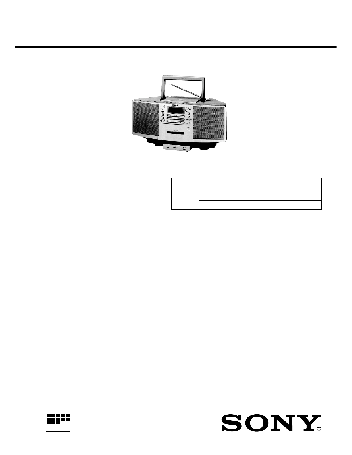
ZS-D5
US Model
Canadian Model
AEP Model
UK Model
E Model
SERVICE MANUAL
PERSONAL AUDIO SYSTEM
MICROFILM
CD Model Name Using Similar Mechanism New
Section Optical Pick-up Name KSM-213CDM/M-S
Tape deck Model Name Using Similar Mechanism PMC-303
Section Tape Transport Mechanism Type MF-D55-144
— Continued on next page —
SPECIFICATIONS
AUDIO POWER SPECIFICATIONS
POWER OUTPUT AND TOTAL
HARMONIC DISTORTION
With 3-ohm load, both channel driven from
150 - 15,000 Hz; rated 3 W per channelminimum RAM power, with no more than
10 % total harmonic distortion in AC
operation.
Other Specifications
CD player section
System
Compact disc digital audio system
Laser diode properties Material: GaALAs
Wave length : 780 nm
Emission duration: Continuous
Laser output: Less than 44.6 µW (This output is
the value measured at a distance of about 200 mm
from the objective lens surface on the optical
pick-up block with 7 mm aperture.)
Spindle speed 200 r/min (rpm) to 500 r/min (rpm) (CLV)
Number of channels 2
Frequency response 20 - 20,000 Hz +0/-1dB
Wow and flutter Below measurable limit
Radio section
Frequency range
US, Canadian FM: 87.6 - 108 MHz
AM: 530 - 1,710 kHz
AEP, UK, E FM: 87.5 - 108 MHz (Italy)
FM: 87.6 - 107 MHz (Other countries)
MW: 531 - 1,602 kHz
LW: 153 - 279 kHz
Aerials FM: Telescopic aerial
AM: Built-in ferrite bar aerial
Cassette-corder section
Recording system 4-track 2 channel stereo
Fast winding time Approx. 120s (sec.) with Sony cassette C-60
Frequency response TYPE1 (normal): 50 - 15,000 Hz
General
Speaker Full range: 8 cm (3 1/4in.) dia., 3 Ω,
cone type x 2
Input LINE IN jack (stereo minijack)
Minimum input level 250 mV
Outputs Headphones jack (stereo minijack)
For 16 - 68 Ω impedance headphones
LINE OUT jack (stereo minijack)
Rated output level 250 mV at load impedance
47 kΩ
OPTICAL DIGIT AL OUT (CD) (optical output
connector)
Wavelength: 630 - 690 nm
Power output (excluding U.S. model)
4.5 W + 4.5 W (3 ohms at 10 % harmonic
distortion in DC operation)
Power requirements For personal component system:
120 V AC, 60 Hz
12 V DC, 8 size D (R20) batteries
For memory back-up:
6 V DC, 4 size AA (R6) batteries
For remote commander:
3 V DC, 2 size AA (R6) batteries
Power consumption AC 25 W
Ver 1.3 2000.2
With SUPPLEMENT (9-923-270-82)
— 2 —
TABLE OF CONTENTS
SAFETY-RELATED COMPONENT WARNING!!
COMPONENTS IDENTIFIED BY MARK ! OR DO TTED LINE WITH
MARK ! ON THE SCHEMATIC DIAGRAMS AND IN THE PARTS
LIST ARE CRITICAL TO SAFE OPERATION. REPLACE THESE
COMPONENTS WITH SONY PARTS WHOSE PART NUMBERS
APPEAR AS SHOWN IN THIS MANUAL OR IN SUPPLEMENTS
PUBLISHED BY SONY.
ATTENTION AU COMPOSANT AYANT RAPPORT
À LA SÉCURITÉ!
LES COMPOSANTS IDENTIFÉS PAR UNE MARQUE ! SUR LES
DIAGRAMMES SCHÉMATIQUES ET LA LISTE DES PIÈCES SONT
CRITIQUES POUR LA SÉCURITÉ DE FONCTIONNEMENT. NE
REMPLACER CES COMPOSANTS QUE PAR DES PIÈSES SONY
DONT LES NUMÉROS SONT DONNÉS DANS CE MANUEL OU
DANS LES SUPPÉMENTS PUBLIÉS PAR SONY.
After correcting the original service problem, perform the
following safety checks before releasing the set to the customer:
Check the antenna terminals, metal trim, “metallized” knobs, screws,
and all other exposed metal parts for A C leakage. Check leakage as
described below.
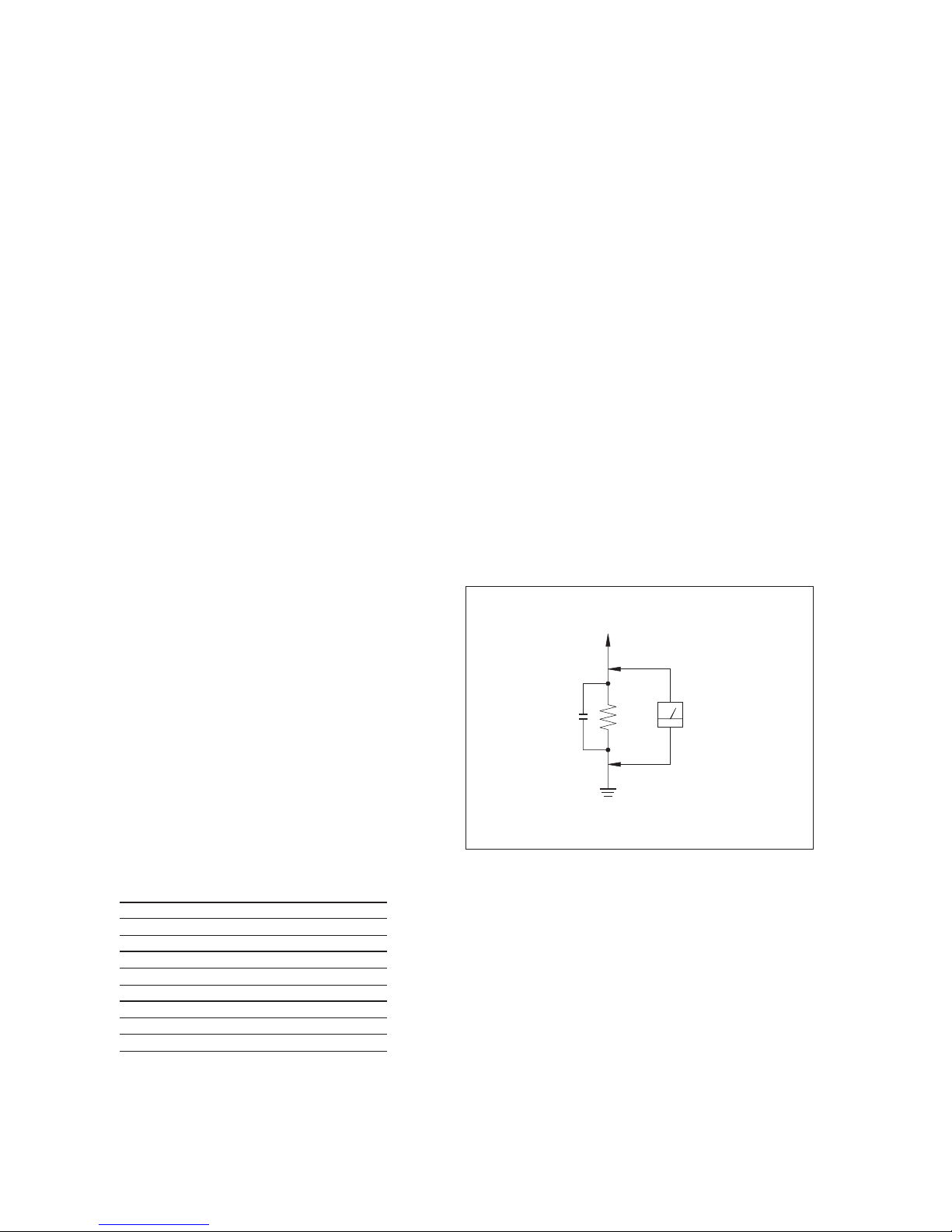
LEAKAGE
The AC leakage from any exposed metal part to earth ground
and from all exposed metal parts to any exposed metal part having
a return to chassis, must not exceed 0.5 mA (500 microamperes).
Leakage current can be measured by any one of three methods.
1. A commercial leakage tester, such as the Simpson 229 or RCA
WT -540A. F ollow the man ufacturers’ instr uctions to use these
instruments.
2. A battery-operated AC milliammeter. The Data Precision 245
digital multimeter is suitable for this job.
3. Measuring the voltage drop across a resistor by means of a
VOM or batter y-operated A C voltmeter . The “limit” indication
is 0.75 V, so analog meters must have an accurate low-voltage
scale. The Simpson 250 and Sanwa SH-63T rd are examples of
a passive VOM that is suitable. Nearly all battery operated
digital multimeters that have a 2V AC range are suitable. (See
Fig. A)
SAFETY CHECK-OUT
1. SERVICE NOTE ...............................................................3
2. GENERAL ..........................................................................4
3. DISASSEMBLY
3-1. Front Cabinet Assy ........................................................... 12
3-2. Mechanisum Assy............................................................. 13
3-3. Control Board, Lump Board, H/P Board ..........................14
3-4. CD Block Assyt, Handole ................................................14
3-5. Main Board, Optical Pick up ............................................ 15
3-6. Tuner Board, Power Board, Rear Cabinet........................ 15
4. TEST MODE .....................................................................16
5. MECHANICAL ADJUSTMENTS ............................. 16
6. ELECTRICAL ADJUSTMENTS ............................... 17
7. DIAGRAMS
7-1. Circuit Boards Location ................................................... 20
7-2. Brock Diagrams – Tuner/CD Section –........................... 21
7-3. Brock Diagrams – TC Section –...................................... 23
7-4. Printed Wiring Board —Main Section — ........................ 26
7-5. Schematic Diagram —Main Section (1/2) — ..................29
7-6. Schematic Diagram —Mainl Section (2/2) — ................. 32
7-7. Printed Wiring Board —Power Section — ...................... 35
7-8. Schematic Diagram —Power Section — ......................... 37
7-9. Printed Wiring Board —Control/Switch Section — ........ 39
7-10. Schematic Diagram —Control/Switch Section — ........... 43
7-11. Printed Wiring Board
—Tuner Section (US, CND model) — ............................45
7-12. Schematic Diagram
—Tuner Section (US, CND model) — ............................47
7-13. Schematic Diagram
—Tuner Section (AEP, IT, UK, E model) — ................... 50
7-14. Printed Wiring Board
—Tuner Section (AEP, IT, UK, E model) — ................... 53
7-15. Schematic Diagram —TC Section — ..............................55
7-16. Printed Wiring Board —TC Section — ........................... 57
7-17. IC Pin Function ................................................................ 58
7-18. IC Brock Diagrams........................................................... 60
8. EXPLODED VIEWS
8-1. Cabinet Section................................................................. 64
8-2. Rear Cabinet Section ........................................................ 65
8-3. CD Mechanism (KSM-213CDM/M-S) ............................66
8-4. Optical Pick up ................................................................. 67
8-5. Cassette Mechanism Deck Section-1 (MF-D55-144) ......68
8-6. Cassette Mechanism Deck Section-2 (MF-D55-144) ......69
9. ELECTRICAL PARTS LIST ........................................70
T o Exposed Metal
Parts on Set
0.15
µ
F
1.5 k
Ω
AC
Voltmeter
(0.75 V)
Earth Ground
Fig. A. Using an A C v oltmeter to check A C leakage.
Battery life
For CD radio cassette-corder
FM recording
Sony R20P: approx. 6 h
Sony alkaline LR20: approx. 12h
Tape playback
Sony R20P: approx. 3h
Sony alkaline LR20: approx. 6h
CD playback
Sony R20P: approx. 1.5 h
Sony alkaline LR20: approx. 3h
Dimmensions (incl. projecting parts)
Approx. 416 x 198.5 x 246 mm (w/h/d)
(16 1/2 x 7 7/8 x 9 3/4 inches)
Mass (incl. batteries) Approx. 5.2 kg (11 lb. 7 oz)
Supplied accessories AC power cord (1)
Remote commander (1)
Design and specifications are subject to change without notice.
— 3 —
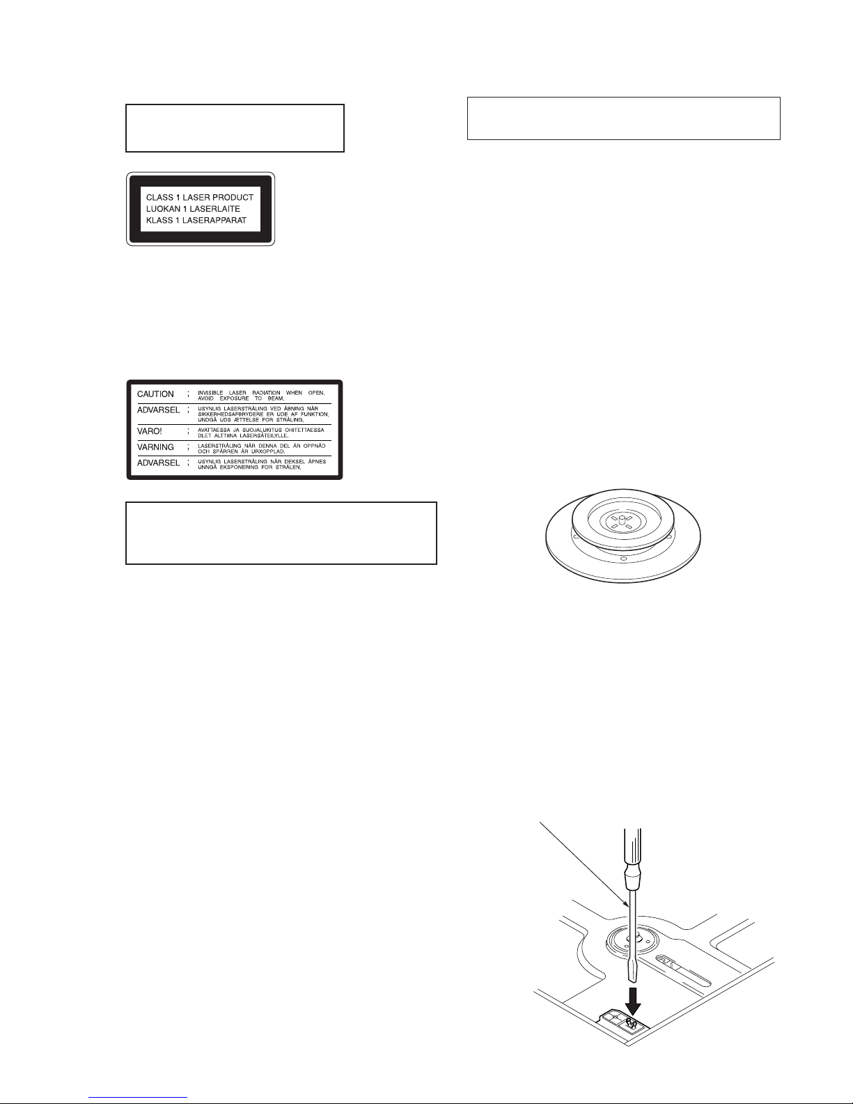
This appliance is classified as a CLASS 1
LASER product. The CLASS 1 LASER
PRODUCT MARKING is located on the rear
exterior.
The following caution label is located inside the
unit.
The laser component in this product is
capable of emitting radiation exceeding the
limit for Class 1.
CAUTION
Use of controls or adjustments or performance of procedures
other than those specified herein may result in hazardous radiation
exposure.
NOTES ON HANDLING THE OPTICAL PICK-UP
BLOCK OR BASE UNIT
The laser diode in the optical pick-up block may suffer electrostatic
breakdown because of the potential difference generated by the
charged electrostatic load, etc. on clothing and the human body.
During repair , pay attention to electrostatic breakdown and also use
the procedure in the printed matter which is included in the repair
parts.
The flexible board is easily damaged and should be handled with
care.
NOTES ON LASER DIODE EMISSION CHECK
The laser beam on this model is concentrated so as to be focused on
the disc reflective surface by the objective lens in the optical pickup block. Therefore, when checking the laser diode emission,
observe from more than 30 cm away from the objective lens.
CHUCK PLATE JIG ON REPAIRING
On repairing CD section, playing a disc without the CD lid, use
Chuck Plate Jig.
• Code number of Chuck Plate Jig : X-4918-255-1
LASER DIODE AND FOCUS SEARCH OPERATION
CHECK
1. Press CD open knob.
2. Open the lid for CD.
3. Push on SWITCH as following figure.
4. Confirm the laser diode emission while observing the objecting
lens. When there is no emission, Auto Power Control circuit or
Optical Pick-up is broken.
Objective lens moves up and down once for the focus search.
SECTION 1
SERVICING NOTE
Insert a precision screw driver
and push SWITCH
— 4 —
SECTION 2
GENERAL
This section is extracted
from instruction manual.
@™
@¡
@º
!ª
!•
!¶
!§
!∞
!¢
9
!º
!¡
!™
!£
12345678
@¢
@§
@∞
@£
@¶
1 MEGA BASS button
2 SOUND button
3 STANDBY button
4 SLEEP button
5 CLOCK button
6 PROGRAM AUTO
PRESET CHECK button
7 MODE MONO/ST ISS button
8 CANSEL button
9 VOL button
0 EDIT button
!¡ DISPLAY ENTER button
@£ PUSH OPEN/CLOSE (CD)
@¢ CD button
@∞ RADIO buttons
!™ TUNE/TIME SET button
!£ MD (LINE) button
!¢ OPTICAL DIGITAL OUT (CD)
!∞ r/P button
!§ COUNTER RESET button
!¶ DIR MODE button
!• TIMER button
!ª Remote sensor
@º OPR/BATT lamp
@¡ POWER button
@™ 2
@§ TAPE buttons
@¶ PUSH OPEN/CLOSE (CASSETTE)
LOCATION OF PARTS AND CONTROLS
— 5 —

— 6 —
— 7 —
— 8 —
— 9 —
— 10 —
— 11 —
— 12 —
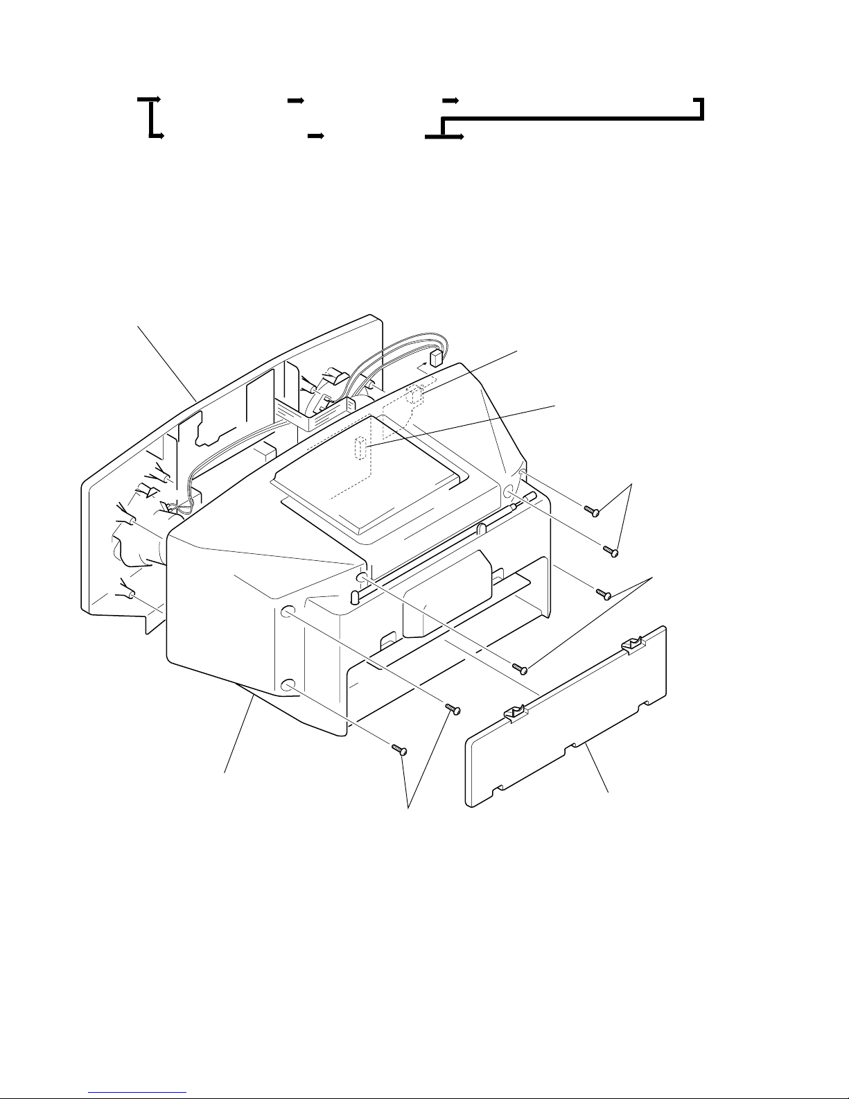
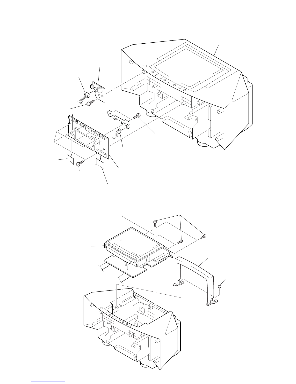
SECTION 3
DISASSEMBLY
3-1. FRONT CABINET ASSY
6
Front cabinet assy
3
Connector(CN306)
4
Connector (CN801)
2
Screws
(+BVTP 3 ×12)
1
Battery lid
2
Screws
(+BVTP 3
×
12)
5
Rear cabinet assy
2
Screws
(+BVTP 3 ×12
)
Note : Follow the disassembly procedure in the numerical order given.
ZS-D5 FRONT CABINET ASSY
MECHANISM DECK ASSY
CONTROL BOARD, LAMP BOARD, H/P BOARD
CD BLOCK ASSY, HANDLE MAIN BOARD,
OPTICAL PICK UP
TUNER BOARD, POWER BOARD, REAR CABINET
— 13 —
3-2. MECHANISM ASSY
Rear cabinet assy
9
Screws
(+BVTP 3
×
10)
9
Screws
(+BVTP 3
×
10
)
8
Connector
(CN402)
5
Connector (CN401)
4
Connector (CN442)
3
Connector (CN441)
7
Terminal board
6
Screws
(+BVTP 2.6
×
10)
1
Screw
(+BVTP 3
×
10)
!¡
Screws
(+BVTP 3
×
10)
!™
MF-D55-144
2
Connector (CN301)
!£
MD chassis
!º
TC board
— 14 —
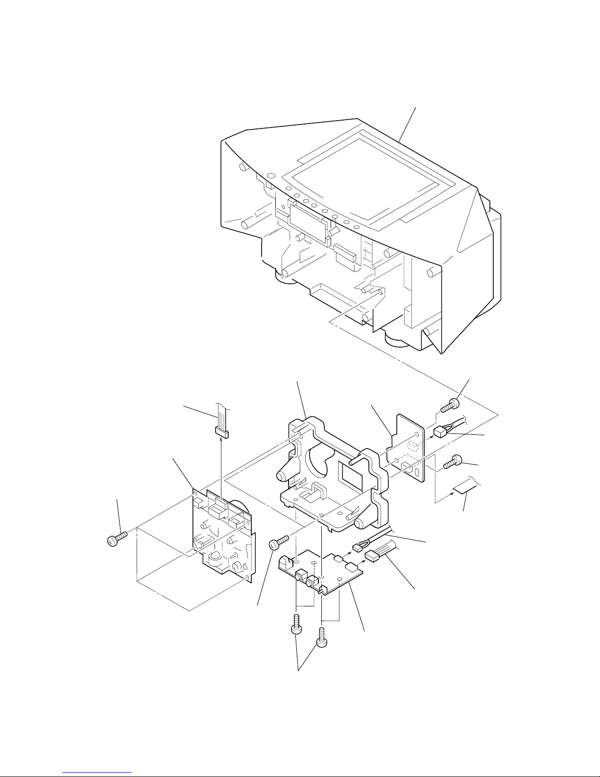
3-3. CONTROL BOARD, LAMP BOARD, H/P BOARD
3-4. CD BLOCK ASSY, HANDLE
Rear cabinet assy
5
Screws
(+BVTP 2.6 ×10)
6
Connector (CN804)
4
CONTROL board
1
Connector (CN803)
3
Screws
(+BVTP 2.6 × 10)
2
Connector (CN802)
7
LANB board
9
Screw
(+BVTP 3 ×10)
8
Connector (CN305)
0
H/P board
2
CD block assy
4
Handle
3
Screws
(+BVTP 3 ×10)
1
Screws
(+BVTP 3 ×10)
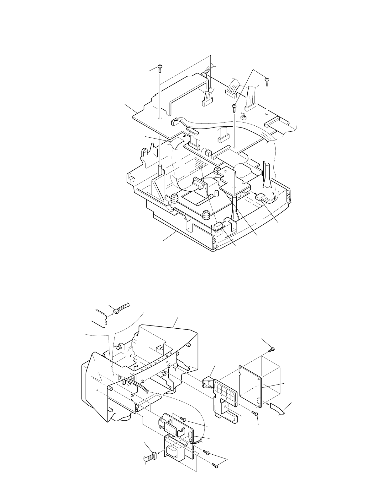
— 15 —
3-5. MAIN BOARD, OPTICAL PICK UP
3-6. TUNER BOARD, POWER BOARD, REAR CABINET
4
Screws
(+BVTP 3 ×10)
4
Screws (+BVTP 3 ×10)
5
MAIN board
1
Connector (CN701)
CD chassis
3
Connector
(POSH SWITCH)
Optical pick up
KSM-213CDM
2
Connecto
r
(CNP703)
0
Rear cabinet
7
Connector (CN904)
6
Connector (CN901)
5
TU cassis
3
Screws (+BVTP 3 ×10)
4
TUNER board
2
Connector (CN1
)
8
Screws
(+BVTP 3 ×10)
9
POWER board
8
Screws
(+BVTP 3 ×10)
1
Screws (+BVTP 3 ×10)
— 16 —
SECTION 4
TEST MODE
SECTION 5
MECHANICAL ADJUSTMENT
1. HOW TO ENTER THE TEST MODE
Turn on the main power. While the machine is in the CD STOP
state, short-circuit JW824 and JW825 on the SWITCH board once.
(Turn off the main power to exit the test mode.)
[SWITCH Board] – Soldering Side –
2. RF Level and Jitter Check
• Measurement Point
MAIN board (see page 9)
Vref (JW126) and RF Signal (JW135)
(Confirm by oscilloscope)
• Procedure
(1) Press the CD key → Press the DISPLA Y ENTER MEMOR Y
key.
(2) Confirm that display on LCD changes as follows.
88 88
(Indication that automatic adjustment is completed)
(3) Press the EDIT key. (APC OFF)
The display ALL disappears.
(4) Confirm that jitter is 9.0 ns or less. Confirm also that the
RF level is from 0.9 to 1.3 Vp-p.
88 88
F– –F
CHECK CHECK ALL
3. Traverse Signal Check
• Measurement Point:
MAIN board (see page 9)
Vref (JW126) and TE Signal (IC701 pin $¶)
(Confirm by oscilloscope)
• Procedure
(1) Press the = or + key.
(2) Check that the traverse level is from 0.3 to 0.5 Vp-p.
PRECAUTION
1. Clean the following parts with a denatured-alchool-moistened
swab:
record/playback head pinch roller
erase head rubber belts
capstans
2. Do not use a magnetized screwdriver for the adjustments.
3. After the adjustments, apply suitable locking compound to the
parts adjusted.
4. The adjustments should be performed with the raged power
supply voltage unless otherwise noted.
Torque Measurement
T ape Tension Measurement
Meter Reading
36 to 61 g•cm
(0.504 to 0.854 oz•inch)
2 to 6 g•cm
(0.028 to 0.084 oz•inch)
36 to 61 g•cm
(0.504 to 0.854 oz•inch)
2 to 6 g•cm
(0.028 to 0.084 oz•inch)
61 to 143 g•cm
(0.854 to 2.002 oz•inch)
Mode
FWD
FWD
back tension
REV
REW
back tension
FF • REW
Torque Meter
CQ-102C
CQ-102RC
CQ-201B
Meter Reading
more than 100 g•cm
(more than 1.38 oz • inch)
more than 100 g•cm
(more than 1.38 oz • inch)
Mode
FWD
REV
Torque Meter
CQ-403A
CQ-403R
JW825
JW824
0.9 to 1.3 Vp-p
0V
A=B
A+B=
0.3 to 0.5 Vp-p
ZS-D5
— 17 — — 18 — — 19 —
SECTION 6
ELECTRICAL ADJUSTMENT
0 dB = 0.775VTAPE RECODER SECTION
PRECAUTION
1. Perform adjustments in the test mode.
2. Demagnetize the record/playback head with a head
demagnetizer.
3. Do not use a magnetized screwdriver for the adjustments.
4. After the adjustments, apply suitable locking compound to the
parts adjust.
5. The adjustments should be performed with the rated power
supply voltage unless otherwise noted.
6. The adjustments should be performed in the order given in this
service manual. (As a general rule, playback circuit adjustment
should be completed before performing recording circuit
adjustment.)
7. The adjustments should be performed for both L-CH and RCH.
• Standard Record:
Deliver the standard input signal level to the input jack and set the
VOLUME +/– keys to obtain the standard input and output signal
level.
• Standard input level
• Standard output level
• Test tape
Record/Playback Head Azimuth Adjustment
Note: • Start adjustment after head has changed the direction.
(When head is positioned in the FWD direction of tape
running, start adjustment with REV .)
• The adjustment must be ended with cw turning of
adjustment screw.
Procedure:
1. Mode : REV playback
LINE IN
10 kΩ
0.25 V (–9.8 dB)
Input Pin
Signal source impedance
Input signal level
Test Tape
P-4-A100
WS-48A
Used for
REC/PB/ERASE Head azimuth
and phase adjustment.
Tape speed adjustment
Signal
10 kHz, -10 dB
3 kHz, 0 dB
Output Pin
Load impedance
Output signal level
SP OUT (L, R) H.P OUT
3.2 32
0.775 V (0 dB) 0.10 V (-18 dB)
Tape Speed Adjustment
Procedure:
Mode : FWD playback
1. Playback the standard tape in FWD mode.
2. Adjust the variable resistor of the motor (M691) until frequency
counter reading is from 2,985 to 3,015 Hz.
3. Confirm that the freqency difference between the tape top and
end is within 3 %.
set
+
–
level mete
r
test tape
P-4-A100
(10KHz, –10dB)
LINE OUT
47
k
Ω
Screw
position
L-CH
peak
within
1dB
output
level
L-CH
peak
R-CH
peak
within
1dB
Screw
position
R-CH
peak
2. Turn the adjustment screw and check output peaks. If the peaks
do not match for L-CH and R-CH, turn the adjustment screw
so that outputs match within 1dB of peak.
3. Phase Check
Mode: REV playback
Note: Adjustment must be completed by cw turning of adjustment
screw.
After the adjustment, lock the screws with locking
compound.
4. Repeat steps 1 to 3 FWD playback mode.
5. Check that phase difference between L-CH and R-CH is from o
to 90 degrees.
6. After the adjustments, apply suitable locking compound to the
pats adjusted.
Adjustment Location:
LINE OUT
test tape
WS-48B
(3 kHz, 0 dB)
set
frequency counter
+
–
100 k
Ω
Oscilloscope Lissajous pattern
in phase
good
wrong
45°
135°90° 180°
test tape P-4-A100
(100 kHz, –10 dB)
L-CH
R-CH 47 k
Ω
LINE
47 k
Ω
oscilloscope
set
V
H
Adjustment screw
(FWD)
Adjustment screw
(REV)
0 dB = 1µV
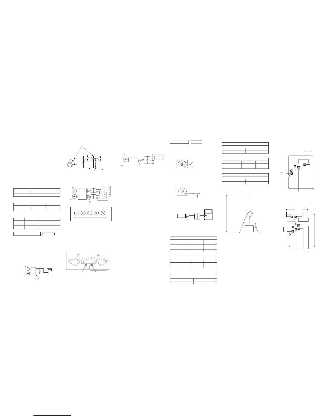
TUNER SECTION
[Setting during adjustment]
Function mode: RADIO
VOLUME: Maximum
• AM Section
• FM section
AM RF SSG
Put the lead-wire antenn
a
close to the set.
30% amplitude
modulation by
400 Hz signal
Output level: as low as possible
to FM RF (FM IN)
FM RF SSG
22.5 kHz frequency
deviation by 400 Hz
signal
Output level: as low as possible
set
32
Ω
VTVM
HEADPHONES
+
–
• Repeat the proceduresin each adjustment several times for the
maximum level meter indication.
• The frequency coverage and tracking adjustments should be
finally done by the trimmer capacitors.
AEP/Italian/UK/E model
LW RECEPTION FREQUENCY COVERAGE CHECK
Frequency indication 151 kHz 273 kHz
Digital voltmeter reading 0.6 to 0.7 V 4.7 to 5.7 V
Adjustment CT3 check
( ) : US/Canadian model
MW/AM TRACKING ADJUSTMENT
Adjust for a maximum defection of level meter.
L3 CT2
621 kHz (620 kHz) 1,404 kHz (1,400 kHz)
( ) : US/Canadian model
MW/AM RECEPTION FREQUENCY COVERAGE CHECK
Frequency indication
531 kHz 1,611 kHz
(530 kHz) (1,710 kHZ)
Digital voltmeter reading
0.6 to 1.2 V 4.5 to 5.5 V
(0.9 to 1.0 V) (5.2 to 6.2 V)
Adjustment L4 check
AEP/Italian/UK/E model
LW TRACKING ADJUSTMENT
Adjust for a maximum defection of level meter.
L3 CT5
162 kHz 261kHz
FM RECEPTION FREQUENCY COVERAGE CHECK
Frequency indication 87.5 MHz 108 MHz
Digital voltmeter reading 0.9 to 1.3 V 3.4 to 4.4 V
Adjustment L2 check
FM TRACKING ADJUSTMENT
Adjust for a maximum defection of level meter.
L1 CT1
87.5 MHz 108 MHz
Adjustment Location: TUNER board (Side A)
[US/CND Model]
IC701
JW12
6
JW135
L3 CT2
AM Tracking
L2: FM Reception
Frequency coverage
CT1
L1
FM
Tracking
L4: AM Reception
Frequency coverage
Measurement Point: MAIN board (Side B)
[AEP/IT/UK/E model]
L3 (LW)
CT5
CT4
L3 (MW)
LW Tracking MW Tracking
L4
CT2
L2: FM Reception
Frequency Coverage
CT1
L1
FM
Tracking
CT3: LW Reception
Frequency
Coverage
MW Reception
Frequency Coverage
ZS-D5
— 20 — — 21 — — 22 —
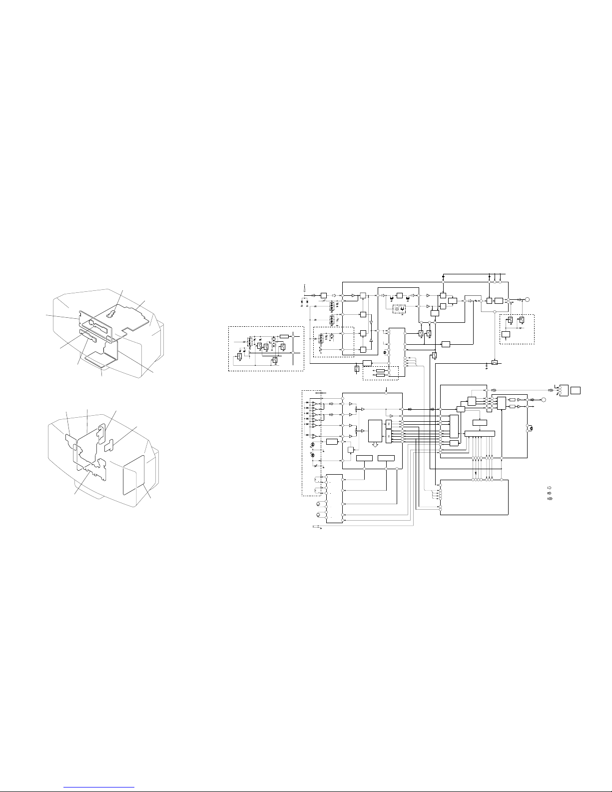
7-1. CIRCUIT BOARD LOCATION
7-2. BLOCK DIAGRAM — TUNER/CD SECTION —
SECTION 7
DIAGRAMS
MAIN board
TC boar
d
TERMINAL board
LAMP board
CONTROL board
CD MOTOR board
SW board
TUNER boar
d
SWITCH board
H/P board
POWER board
BATTERY(L)board
BATTERY(S)board
19
B.P.F
FL1
L1
AU7.5V
L2
L3
FERRITE-ROD
ANTENNA
AU7.5V
AU7.5V
D1
D2
D3
ANTENNA
ANT1
FM
TELESCOPIC
1
23
21
24
22
FM
MIX
FM RF I
FM RF O
FM OSC
AM RF
AM OSC
FM
OSC
AM
MIX
AM
OSC
OSC
3
MIX OUT
17
RF IF
AMP
IF
BUFFER
Q18(US,CND)
CF1 CF2
CFT1
6
7
FM IF
AM IF
FM
MPX
FM/AM
BUFFER
FM
DET
AM
DET
16
A
MPX
18
MUTE
11
12
10
ST IND
TU5V
R-CH
9
FM/AM FRONT-END
IC1
13 22 5
AU7.5V
QUAD
VCO VCC1VCC2
TO
TC SECTION
CF4CF3
H FREQ
CUT
Q1(US,CND)
B
TO
TC SECTION
CE
17
21
10
16
1898
Q3(US,CND)
14 15
MO/ST
BAND
14
7
6
5
4
1
2
PLL
L.P.F
Q17(US,CND)
+B
Q19(US,CND)
PLL
IC3(US,CND)
FM
AM
VDD
XO
XI
PD1
CK
DA
CD
IF
P0
P1
Q4(US,CND)
TU5V
X1
75kHz
CE
CK
DA
CD
OPTICAL PICK-UP
BLOCK
(KSM-213CDM/M-S)
LD/POWER
CONTROL
Q701
41
VCC
CD5V
A
VC
C
B
D
E
F
VC
LD
GND
A
C
B
D
E
F
FOCUS
COIL
F+
F
T+
T
TRACKING
COIL
36
37
42
39
38
51
APC
FOCUS PHASE
COMPENSATION
DECODER
SERIAL/
PARALLEL
CONVERTER
FE
AMP
RF
AMP
IIL
TTL
TTL
IIL
COMAND
VC
TRACKING PHASE
COMPENSATION
LD
PD
E
F
PD1
PD2
6
25
24
26
21
20
23
22
33
27
SENS 1
SENS 2
19
RFO
FOK
C OUT
DATA
XLT
CLK
XRST
LOCK
1613
FEO TEO SLO
IC703
F/T COIL
SL/SP MOTOR
DRIVER
CD RF/SERVO
PROSSESOR
IC701
18
VCC
CD5V
10
4
T IN
9
7
6
VR
PD
PD
28
27
22
21
11
F IN
29
SL IN
25
SP IN
15
MUTE
F+
F
T+
T
SL+
SL
SP+
SP
M
M
MOTOR
M702
SLED
MOTOR
M701
SPINDOL
S701
LIMIT
EFM
DEMO.
44
23
14
13
15
16
17
100
29
27
22
18
XRST
CLV
SERVO
DIGITAL
CLV
D/A
I/F
SUB CODE
PROSSESOR
CPU I/F
50
10 11 12 7 8 9 8075
LOCK
MDP
XLON
SPOA
SENS
SCOR
SQSO
SQCK
CLOCK
XLAT
DATA
CLK
XLT
DAT
SE
CN
FOK
RF
72
54
52
51
73
55
53
SERIAL
I/F
PWM
PWM
71
84
95
89
90
D OUT
PCMD
BCK
LRCK
EMPH
AL
AR
XTAI
XTAO
X701
SYSM
VDD
R-CH
L-CH
D IN
GND
2
1
3
CD5V
OPTICAL
DIGITAL
OUT
IC441
L-CH
5
C XLAT
6
C DATA
8
C CLK
11
C SQCK
12
C SQSO
9
C SENSE1
1
C SCOR
7
B MUTE
25
R CONT
23
R DATA
22
R CLK
24
R CE
13
C SENSE2
4
C XRST
21
R ST
CD
DA
CK
CE
IC801(1/2)
SYSTEM CONTROL
CD DIGITAL
SIGNAL PROCESSOR
IC702
16
:FM
:CD
:DIGITAL OUT
• SIGNAL PATH
Q15
MUTE
SWITCH
MUTE
Q16
MUTE
AU7.5V
Q18
TU7.5V
AEP,IT,UK,E
Q23(AEP,IT,UK,E)
US,CND Model
PD1
Q14(AEP,IT,UK,E)
11
INV.
INV.
MW-H
LW-H
Q22
Q21
MW-L
LW-L
AEP,IT,UK,E Model
Q13(AEP,IT,UK,E)
IC2(AEP,IT,UK,E)
Q12(AEP,IT,
UK,E)
Q2(US,CND)
Q10(AEP,IT,
UK,E)
Q9(AEP,IT,UK,E)
Q11(AEP,IT,UK,E)
Q15(US,CND)
Q17(AEP,IT,UK,E)
D5
L3
FERRITE-ROD
ANTENNA
24
22
Q6
Q2
BUFFER
MW-H
Q1
LW-H
AU7.5V
AM RF
PD1
AM OSC
Q5
Q4
Q3
AEP,IT,UK,E Model
Q13
IC 1
Q22
Q21
• R-CH:Same as L-CH
• Abbreviation
CND : Canadian
IT : Italian
 Loading...