

Sony XVMR-90-D Service manual
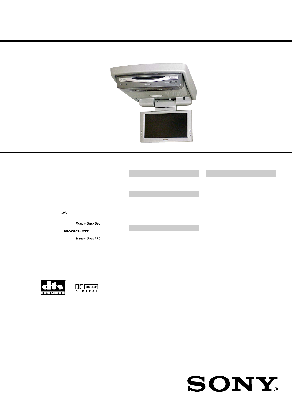
XVM-R90D
System
Laser Semiconductor laser
Signal format system NTSC/PAL
Audio characteristics
Frequency response 20 Hz to 20 kHz
Signal to noise ratio 90 dB (A)
Harmonic distortion 0.05 %
Dynamic range 90 dB
Wow and flutter below measurable limits
(±0.001% W PEAK)
General
Outputs FM output
Audio output
Video output
Optical output
Inputs Audio input
Video input
DC 12V input
Power requirements 12 V DC
Dimensions Approx. 285 × 73 × 455 mm
(w/h/d)
Mass Approx. 3.5 kg
Operating temperature 0 ˚C to 45 ˚C
Supplied accessories Card remote commander
RM-X137
Power supply lead (1)
RF modulator cable (1)
Mounting plate (1)
Screws (5)
Tapping screws (8)
Operating Instructions (1)
Monitor
System Liquid crystal colour
display
Display Manual flipdown panel
Drive system TFT-LCD active matrix
system
Picture size 9 inches wide screen (16:9)
Picture segment 336,960 (w 1,440 × h 234)
dots
Design and specifications are subject to change
without notice.
SERVICE MANUAL
Ver 1.0 2004.07
Copyrights
This product incorporates copyright protection
technology that is protected by method claims
of certain U.S. patents, other intellectual
property rights owned by Macrovision
Corporation, and other rights owners. Use of
this copyright protection technology must be
authorized by Macrovision Corporation, and is
intended for home and other limited viewing
uses only unless otherwise authorized by
Macrovision Corporation. Reverse engineering
or disassembly is prohibited.
•“Memory Stick,”
Memory Stick” are trademarks of Sony
Corporation.
•“Memory Stick Duo” and “
are trademarks of Sony Corporation.
•“MagicGate” and “
trademarks of Sony Corporation.
•“Memory Stick PRO” and “
are trademarks of Sony Corporation.
Manufactured under license from Dolby
Laboratories. “Dolby”, “Pro Logic”, and the
double-D symbol are trademarks of Dolby
Laboratories.
“DTS,” “DTS Digital Surround” and “DTS
Digital Out” are trademarks of Digital Theater
Systems, Inc.
and “MagicGate
”
” are
”
E Model
SPECIFICATIONS
9-879-085-01
2004G05-1
© 2004.07
OVERHEAD DVD ENTERTAINMENT SYSTEM
Sony Corporation
e Vehicle Company
Published by Sony Engineering Corporation
XVM-R90D
CAUTION
The use of optical instruments with this
product will increase eye hazard.
CAUTION
Use of controls or adjustments or performance of procedures
other than those specified herein may result in hazardous radiation
exposure.
Notes on chip component replacement
• Never reuse a disconnected chip component.
• Notice that the minus side of a tantalum capacitor may be
damaged by heat.
Flexible Circuit Board Repairing
• Keep the temperature of the soldering iron around 270 ˚C
during repairing.
• Do not touch the soldering iron on the same conductor of the
circuit board (within 3 times).
• Be careful not to apply force on the conductor when soldering
or unsoldering.
This label is located on the bottom of the
chassis.
CAUTION INVISIBLE
VIEW DIRECTLY WITH OPTICAL INSTRUMENTS
This label is located on the drive unit’s internal
chassis.
LASER RADIATION WHEN OPEN
DO NOT STARE INTO BEAM OR
TABLE OF CONTENTS
1. SERVICING NOTES ................................................ 3
2. GENERAL
Location of Controls........................................................ 5
3. DISASSEMBLY
3-1. Disassembly Flow ........................................................... 7
3-2. Bracket (Main) ................................................................ 7
3-3. DVD Mechanism Deck Block......................................... 8
3-4. MAIN Board.................................................................... 8
3-5. Rear Cover (Hinge) ......................................................... 9
3-6. LCD Block ...................................................................... 9
3-7. LCD Board ...................................................................... 10
3-8. Liquid Crystal Display Panel (LCD1) ............................. 10
4. TEST MODE.............................................................. 11
5. ELECTRICAL ADJUSTMENTS ......................... 12
6. DIAGRAMS
6-1. Block Diagram – MPEG DECODER Section – ............ 17
6-2. Block Diagram – AUDIO Section – ............................... 18
6-3. Block Diagram – VIDEO, PANEL Section –................. 20
6-4. Block Diagram – POWER SUPPLY Section – .............. 21
6-5. Printed W iring Board
– MAIN Board (Component Side) – ............................... 22
6-6. Printed W iring Board
– MAIN Board (Conductor Side) – ................................. 23
6-7. Schematic Diagram – MAIN Board (1/4) – ................... 24
6-8. Schematic Diagram – MAIN Board (2/4) – ................... 25
6-9. Schematic Diagram – MAIN Board (3/4) – ................... 26
6-10. Schematic Diagram – MAIN Board (4/4) – ................... 27
6-11. Printed Wiring Board – LCD Board (Side A) – ............. 28
6-12. Printed Wiring Board – LCD Board (Side B) – ............. 29
6-13. Schematic Diagram – LCD Board (1/4) – ...................... 30
6-14. Schematic Diagram – LCD Board (2/4) – ...................... 31
6-15. Schematic Diagram – LCD Board (3/4) – ...................... 32
6-16. Schematic Diagram – LCD Board (4/4) – ...................... 33
6-17. Printed Wiring Board – PANEL Section (1/2) – ............ 34
6-18. Printed Wiring Boards – PANEL Section (2/2) – ........... 35
6-19. Schematic Diagram – PANEL Section –........................ 36
7. EXPLODED VIEWS
7-1. Skirt (Cabinet) Section .................................................... 52
7-2. Front (Panel) Section ....................................................... 53
7-3. MAIN Board Section....................................................... 54
7-4. Cabinet (Base) Section .................................................... 55
7-5. LCD Section.................................................................... 56
8. ELECTRICAL PARTS LIST................................ 57
2

SECTION 1
SERVICING NOTES
XVM-R90D
NOTES ON HANDLING THE OPTICAL PICK-UP
BLOCK OR BASE UNIT
The laser diode in the optical pick-up block may suffer electrostatic
break-down because of the potential difference generated by the
charged electrostatic load, etc. on clothing and the human body.
During repair, pay attention to electrostatic break-down and also
use the procedure in the printed matter which is included in the
repair parts.
The flexible board is easily damaged and should be handled with
care.
NOTES ON LASER DIODE EMISSION CHECK
Never look into the laser diode emission from right above when
checking it for adjustment. It is feared that you will lose your sight.
UNLEADED SOLDER
Boards requiring use of unleaded solder are printed with the leadfree mark (LF) indicating the solder contains no lead.
(Caution: Some printed circuit boards may not come printed with
the lead free mark due to their particular size)
: LEAD FREE MARK
Unleaded solder has the following characteristics.
• Unleaded solder melts at a temperature about 40 ˚C higher
than ordinary solder.
Ordinary soldering irons can be used but the iron tip has to be
applied to the solder joint for a slightly longer time.
Soldering irons using a temperature regulator should be set to
about 350 ˚C.
Caution: The printed pattern (copper foil) may peel away if
the heated tip is applied for too long, so be careful!
• Strong viscosity
Unleaded solder is more viscou-s (sticky, less prone to flow)
than ordinary solder so use caution not to let solder bridges
occur such as on IC pins, etc.
• Usable with ordinary solder
It is best to use only unleaded solder but unleaded solder may
also be added to ordinary solder.
3
XVM-R90D
About discs this player can
play
This player can play the following discs:
•DVD
•DVD-R/DVD-RW
•Video CD
•Audio CD
•CD-R/CD-RW
Disc type Label on the disc
DVD VIDEOs
Video CDs
Region code of DVDs this player
can play
This player has a region code printed on the
rear of the player and will only play DVDs that
are labelled with identical region codes. DVDs
labelled
If you try to play any other DVD, the message
“REGION ERROR” will appear on the screen.
Depending on the DVD, the region code
indication may not appear even if the DVD is
prohibited by area restrictions.
ALL
will also be played on this player.
Region
code
Audio CDs
MP3 files/
JPEG files
“DVD VIDEO,” “DVD-R” and “DVD-RW” are
trademarks.
Notes on CD-Rs (recordable CDs)/
CD-RWs (rewritable CDs)/DVD-Rs
(recordable DVDs)/DVD-RWs
(rewritable DVDs)
•Some CD-Rs/CD-RWs/DVD-Rs/DVD-RWs
(depending on the equipment used for its
recording or the condition of the disc) may
not play on this player.
•You cannot play a CD-R/CD-RW/DVD-R/
DVD-RW that is not finalized*.
•You cannot play a CD-R/CD-RW that is
recorded in Multi Session.
•You can play MP3/JPEG files recorded on
CD-ROMs, CD-Rs, and CD-RWs.
* A process necessary for a recorded CD-R/CD-RW
disc to be played on the audio CD player.
Cautions
• This player CANNOT play these discs.
— DVD-Audio — DVD-RAM
— DVD-ROM — CD-G
— SVCD — CD-I
— Photo-CD — VSD
— Active-Audio (Data)
— CD-Extra (Data)
— Mixed CD (Data)
— CD-ROM (the data other than the MP3/JPEG
file)
— DVD-RW recorded in VR mode
• This product incorporates copyright protection
technology that is protected by method claims of
certain U.S. patents and other intellectual
property rights owned by Macrovision
Corporation and other rights owners. Use of this
copyright protection technology must be
authorized by Macrovision Corporation, and is
intended for home and other limited viewing
uses only unless otherwise authorized by
Macrovision Corporation. Reverse engineering or
disassembly is prohibited.
Note on PBC (Playback Control)
This player conforms to Ver. 1.1 and Ver. 2.0 of
Video CD standards. You can enjoy two kinds
of playback according to the disc type.
Disc type
Video CDs without
PBC functions
(Ver. 1.1 discs)
Video CDs with
PBC functions
(Ver. 2.0 discs)
You can
Video playback (moving
pictures) as well as music.
•Interactive software
with menu screens
displayed on the
monitor
•Video playback
functions.
•High-resolution still
pictures if they are
included on the disc.
4
Location of controls
1
2
3
4
5
6
7
8
SECTION 2
GENERAL
9
0
qa
qs
qd
qf
qg
qh
XVM-R90D
This section is extracted from
instruction manual.
Refer to the pages listed for details.
1 Disc slot
2 POWER (on/off) button
To turn on/off the player.
3 DISC IN light
When a disc is in the player, the DISC IN
light glows orange.
4 RESET button
5 . (previous)/> (next) buttons
6 Receptor for the card remote
commander/Transmitter for the cordless
headphones
7 Monitor
8 VOL +/– buttons
To turn up or down the volume or to select
the item during menu operation.
9 EJECT button
Available to eject a disc from the player
even when the player is turned off.
q; “Memory Stick” slot
qa x (stop) button
qs u (play/pause) button
qd OPEN button
Slide to open the monitor.
qf Speakers (left/right)
qg REVERSE button
To switch images upside down and
reverse the output of the audio channels.
qh MENU button
To make various display settings and FM
modulator setting.
Note
Even when the player is turned off by pressing
(POWER), you can eject a disc from the player,
though you cannot insert a disc.
XVM-R90D
Card remote commander RM-X137
ENTER
INPUT
POWER
SEARCH
CLEAR
SUBTITLE
ANGLE
AUDIO
SETUP
DISPLAY
123
456
7 890
TOP MENU
MENU
VOL
The corresponding buttons of the card
remote commander control the same
functions as those on the player.
Instructions in this manual describe how to use
the player by mainly using the card remote
commander.
Tip
Refer to “Replacing the lithium battery” for details
on how to replace the battery.
Refer to the pages listed for details.
1 DISPLAY button
To display the time information of the disc.
2 Number buttons (0 to 9)
3 TOP MENU button
To display the top menu of a recorded
DVD.
4 MENU button
To display the recorded DVD menu, or to
turn on/off the PBC (Playback control)
menu of a Video CD.
5 O (return) button
6 ./> (previous/next) buttons
7 m (fast reverse)/
M (fast forward) buttons
8 M/,/m/< buttons
9 POWER (on/off) button
To turn on/off the player.
q; SEARCH button
To specify a desired point on a disc by
chapter, title, or track.
qa CLEAR button
qs SUBTITLE button
To change the subtitle language while
playing a DVD.
qd ENTER button
To enter a setting.
qf ANGLE button
To select the multiple angles of view while
playing a DVD.
qg AUDIO button
To change the audio output/audio
language.
(slow reverse)/ y (slow forward)
qh
buttons
qj u (play/pause) button
qk x (stop) button
ql SETUP button
Used to perform menu operations.
w; INPUT button
To select the input source.
wa VOL (–/+) buttons
To turn up or down the volume.
5
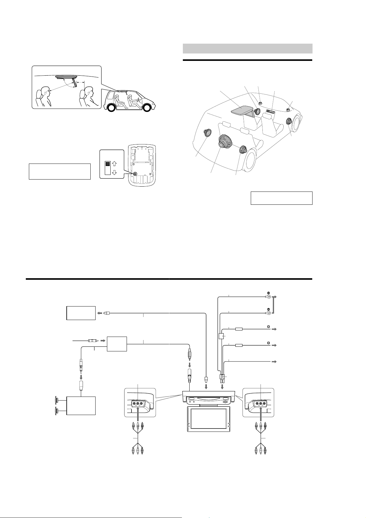
XVM-R90D
Where to install
Before installing this unit, please check your local traffic rules and regulations. Follow the diagram
below to install this unit in a suitable position in your car.
Do not install this unit where:
— It will obstruct the driver’s view when the
monitor is in either the open or closed
position.
— It will obstruct the operation of the airbag
system.
— It will obstruct the operation of the
vehicle, especially the steering wheel, shift
lever, or brake pedal.
—A driver or passengers may injure
themselves when getting into or out of the
car.
If you have any questions or problems
concerning your unit that are not covered
in this manual, please consult your
nearest Sony dealer.
Before installing
Make sure that the POWER SELECT switch is
set to the correct position.
A*: If your car has an accessory position on
the ignition key.
B : If your car has no accessory position on
the ignition key.
* A is the factory preset position.
When the POWER SELECT switch is
set to B
Press (POWER) on the player to turn on.
The player does not turn on by pressing
(POWER) on the card remote commander.
POWER SELECT
switch
B
A
Note
Be sure to turn off the player after driving your
car.
To turn off the player, follow the operations
below:
– Press (POWER) on the player.
– Press (POWER) on the card remote commander.
If the power is left on, it will cause battery drain.
Connections
Installation diagram
Refer to the installation diagram and ask a qualified technician for the installation of the unit.
Front Left
Tweeter Left
Rear Right
speaker
speaker
Note
All equipment other than one DVD player is
optional.
Head unit
Be sure to securely fasten all equipment to
the car chassis, etc., to prevent them
moving while your car is in motion.
Tweeter Right
Front Right
speaker
Rear Left
speaker
XVM-R90D
Subwoofer
Connection diagram
Refer to the connection diagram for the proper connections.
Note
Set the POWER SELECT switch before installing (page 6).
Amplifier equipped
with a digital input
(optional)
From the car aerial
0.5 m
Aerial connector*
Speaker system
(optional)
*1An adapter (optional) may be necessary for your
car and car audio system. In such a case, consult
your dealer.
2
If your car has no ACC (accessory) position on
*
the ignition key switch, set the POWER SELECT
switch to B (page 6) and connect this ACC cable
to the +12 V power (battery) terminal.
1
Car audio
(optional)
RCA pin cord (not supplied)
On AUDIO/VIDEO OUTPUT
connectors
You can connect a Monitor to the AUDIO/
VIDEO OUTPUT connectors to output the
contents being played back on the player.
Relay box
Optical cable
(not supplied)
5 m
AUDIO/VIDEO OUTPUT
Black
Black
Yellow
Fuse (5 A)
Filter box
Red
Fuse (1 A)
Blue
4 Pin Power connector
GND (1 m)
GND (1 m)
Back-up (5 m)
ACC (5 m)
POWER REM (5 m)
Max. supply current 0.3 A
AUDIO/VIDEO INPUT
On AUDIO/VIDEO INPUT connectors
You can connect a VTR, etc. to the AUDIO/
VIDEO INPUT connectors to input the
contents being played back on the device.
To a metal surface
of the car chassis
To car battery
(12 V)
To ignition switch*
(ACC position)
To a power
amplifier
RCA pin cord (not supplied)
2
6
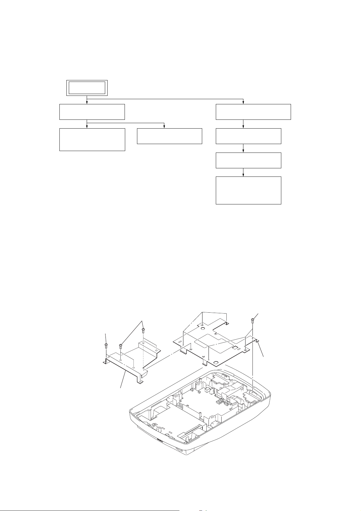
• This set can be disassembled in the order shown below.
)
3-1. DISASSEMBLY FLOW
SET
XVM-R90D
SECTION 3
DISASSEMBLY
3-2. BRACKET (MAIN)
(Page 7)
3-3. DVD MECHANISM
DECK BLOCK
(Page 8)
Note: Follow the disassembly procedure in the numerical order given.
3-4. MAIN BOARD
(Page 8)
3-2. BRACKET (MAIN)
3-5. REAR COVER (HINGE)
(Page 9)
3-6. LCD BLOCK
(Page 9)
3-7. LCD BOARD
(Page 10)
3-8. LIQUID CRYSTAL
DISPLAY PANEL
(LCD1)
(Page 10)
2
two screws
(BTP2.6
3
bracket (support)
×
8)
1
four screws
(B2.6
4
six screws
(BTP2.6
×
4)
×
8)
5
bracket (main
7
XVM-R90D
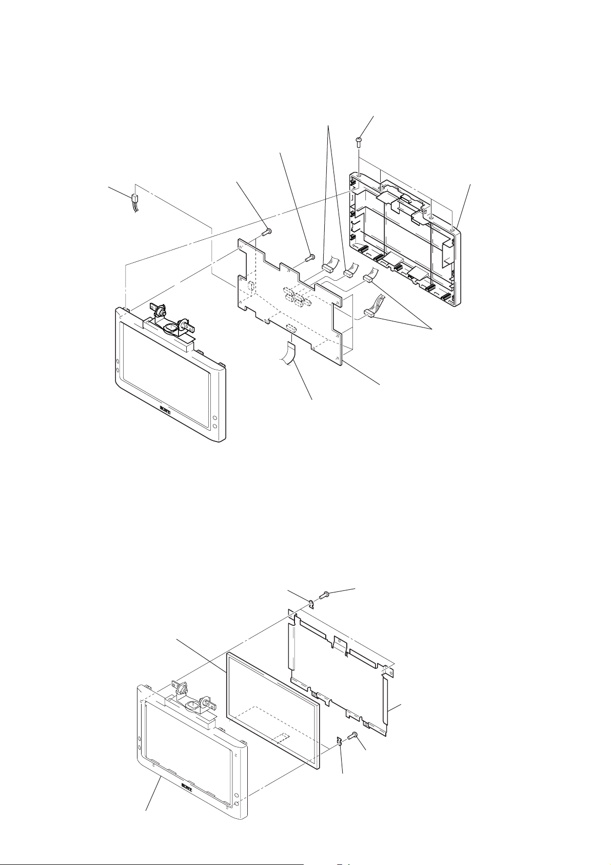
3-3. DVD MECHANISM DECK BLOCK
2
4
bracket (front)
6
two screws
(BTP2.6
DVD mechanism deck block
×
6)
3
two screws
(BTP2.6
5
×
8)
two screws
(BTP2.6
×
8)
3-4. MAIN BOARD
3
three screws
(BTP2.6
1
flexible flat cable
(30P) (CN102)
2
connector (CN702)
×
8)
5
MAIN board
3
screw
(BTP2.6
1
flexible flat cable
(50P) (CN101)
2
connector (CN108)
×
8)
4
harness
2
connector (CN105)
2
connector (CN107)
2
connector (CN302)
2
connector (CN103)
2
connector (CN104)
2
connector (CN701)
2
connector (CN705)
1
flexible flat cable
(50P) (CN101)
8
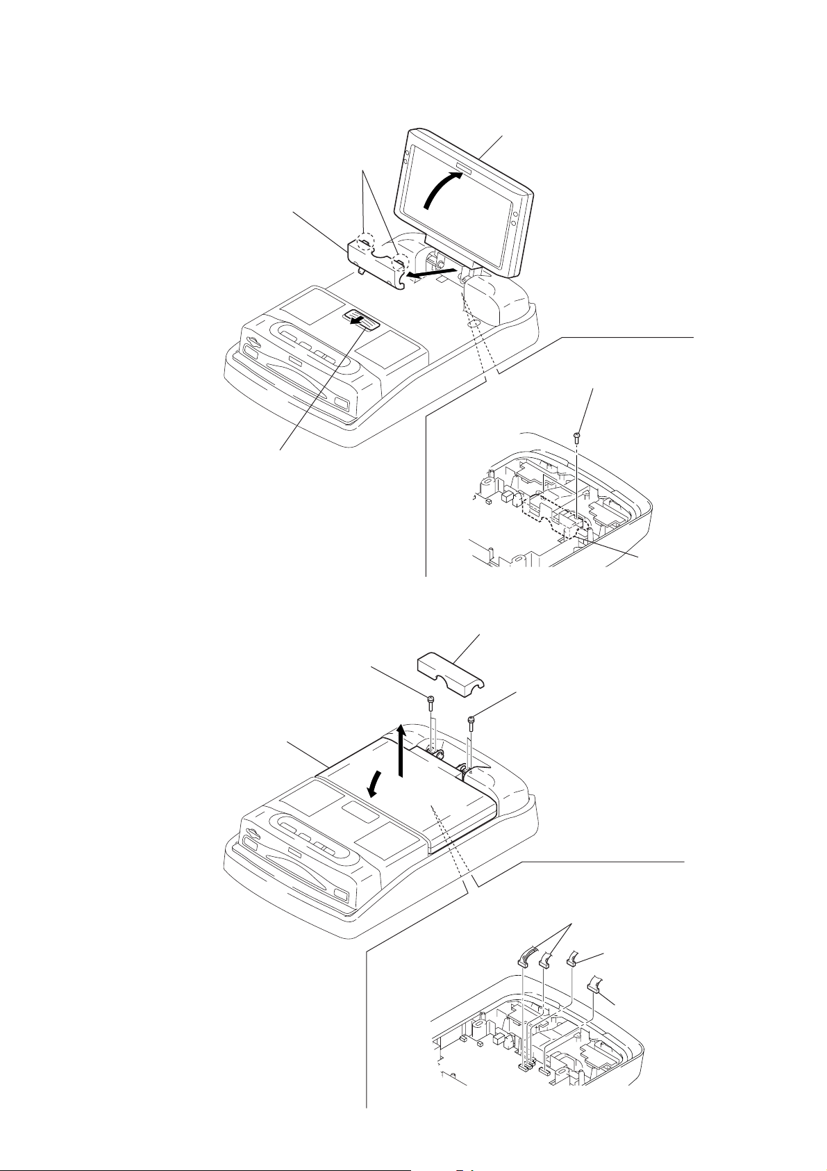
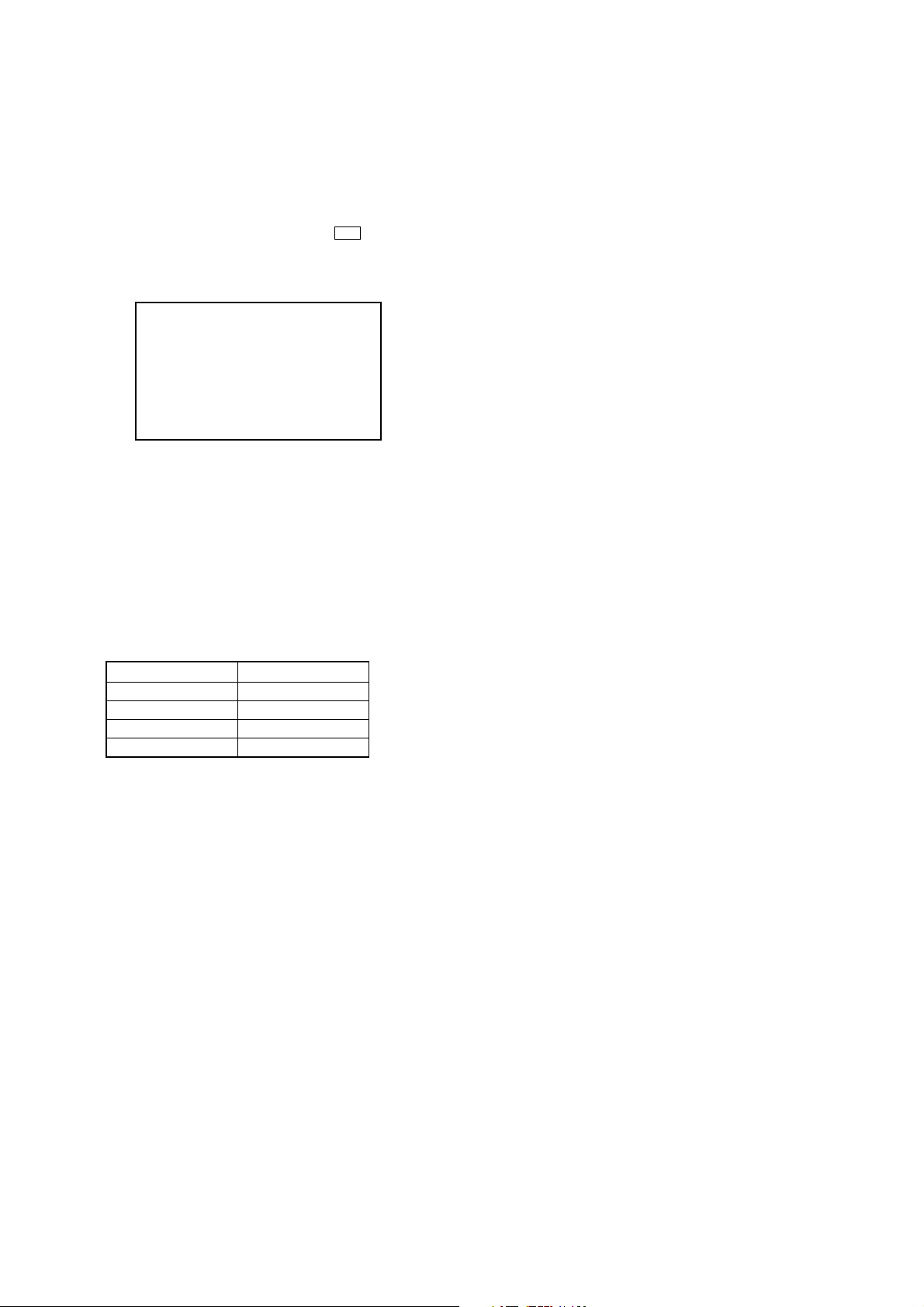
3-5. REAR COVER (HINGE)
4
rear cover (hinge)
3
two claws
A
B
LCD block
2
two screws
(P2 × 8)
XVM-R90D
1
Slide the knob (open) in the direction
of arrow A, and open the LCD block
in the direction of arrow B.
3-6. LCD BLOCK
5
4
two screws
(PS3
Lifting up the LCD block in
the direction of arrow
A
.
×
10)
1
A
3
front cover (hinge)
4
two screws
(PS3
×
rear cover
(hinge)
10)
2
two connectors
(CN105, 108)
2
connector
(CN107)
2
connector
(CN103)
9
XVM-R90D
3-7. LCD BOARD
4
connector
(CN850)
5
eight screws
(BTP2 × 6)
6
screw
(PS2.6 × 6)
4
two connectors
(CN906, 907)
1
four screws
(B2 × 5)
2
rear case (LCD)
3-8. LIQUID CRYSTAL DISPLAY PANEL (LCD1)
2
two retainers (LCD)
6
liquid crystal display panel (LCD1)
3
flexible board
(CN801)
1
two screws
(BTP2 × 6)
7
LCD board
4
two connectors
(CN905, 908)
10
front case (LCD) block
4
5
two retainers
(LCD)
3
two screws
(BTP2 × 6)
shield plate
(LCD)
SECTION 4
TEST MODE
XVM-R90D
Note: This set is able to setting the adjustment data, reset to factory default
and initialize the EEPROM (IC402 on the MONITOR board) in the
test mode.
ENTER THE TEST MODE
Procedure:
1. Press the [POWER] button to turn the power ON.
2. While pressing the [VOL --] and . buttons, press the
[RESET] button.
3. The set is enter the test mode and display as bellow figure.
Display
TEST MODE MENU
1. NTSC/PAL SELECT
2. FOR FACTORY
3. LCD SETTING
4. FM TRANSMITTER
5. HEAT PROTECTION
6. VOLTAGE SETUP
7. LOAD DEFAULT
8. SOFT RESET(EXIT)
Dream System 20XX
Ver.20XX-XX-XXx
Note: If initial data is not written to the EEPR OM (IC402 on the MONITOR
board) or data is clobbered, the set is not able to display normally
screen.
BATCH WRITING OF THE INITIAL DATA TO
EEPROM
In the test mode, by pressing the [VOL --] button at two seconds,
batch writing is possible of the initial data to EEPOM (IC402 on
the MONITOR board).
3. LCD SETTING
This mode is not used in servicing.
4. FM TRANSMITTER
In this mode, switch the frequency range of FM transmitter as
follow.
1) USA (88.3 to 89.9 MHz)
2) Japan (76.5 to 79.5 MHz)
3) Transmitter off
5. HEAT PROTECTION
This mode is not used in servicing.
6. VOLTAGE SETUP
This mode is not used in servicing.
7. LOAD DEFAULT
This mode is not used in servicing.
8. SOFT RESET (EXIT)
Releasing the test mode.
OPERATION OF THE TEST MODE
All operations are performed using the bellow buttons.
Button Function
MENU Select the item
REVERSE Enter
VOL + Up the data value
VOL − Down the data value
RELEASING THE TEST MODE
In the test mode menu screen, press the [MENU] button to select “8.
SOFT RESET (EXIT)”, and press the [REVERSE] button to release
the test mode.
OPERATING THE EACH ITEM
1. NTSC/PAL SELECT
In this mode, switch the signal format system to NTSC or P AL.
2. FOR FACTORY
In this mode, change the data of adjustment data.
Enter this mode, it displays each adjustment item as follow.
1) Com Gain
2) Y Gain
3) Black Limit
4) White Limit
5) R-Sub BRT
6) B-Sub BRT
7) R-Sub CONT
8) B-Sub CONT
9) Gamma 1
10) Gamma 2
11) VCO Free Run
12) PLL/V Pos
13) H Pos
11
XVM-R90D
r
r
r
r
r
r
SECTION 5
ELECTRICAL ADJUSTMENTS
1. DC/DC CONVERTER ADJUSTMENT
1-1. Frequency Adjustment
Setting:
oscilloscope
or
frequency counte
MONITOR board
TP802
TP804
Procedure:
1. Connect an oscilloscope or frequency counter to the TP802
and TP804 on the MONITOR board.
2. Check that the voltage between TP951 (−) and TP952 (+) is
14.4 V. Press the [POWER] button to turn the power on.
3. Adjust the RV801 on the MONITOR board so that the value
of oscilloscope or frequency counter becomes 243 kHz ±3
kHz.
1-2. 5V Voltage Adjustment
Setting:
MONITOR board
TP807
TP804
Procedure:
1. Connect a digital voltmeter to the TP804 and TP807 on the
MONITOR board.
2. Check that the voltage between TP951 (–) and TP952 (+) is
14.4 V. Press the [POWER] button to turn the power on.
3. Adjust the RV803 on the MONITOR board so that the value
of digital voltmeter becomes 5.05 V ±0.03 V.
1-3. Other Voltages Check
Setting:
MONITOR board
TP805/TP806/TP808
TP804
Procedure:
– Vdd Voltage Check –
1. Connect a digital voltmeter to the TP804 and TP808 on the
MONITOR board.
2. Check that the voltage between TP951 (–) and TP952 (+) is
14.4 V. Press the [POWER] button to turn the power on.
3. Check that the value of digital voltmeter is 3.45 V ±0.2 V .
– Vgh Voltage Check –
4. Connect the digital voltmeter to the TP804 and TP806 on the
MONITOR board.
5. Check that the value of digital voltmeter is 17.5 V ±1.5 V .
– Vss Voltage Check –
6. Connect the digital voltmeter to the TP804 and TP805 on the
MONITOR board.
7. Check that the value of digital voltmeter is –12.0 V ±1.5 V.
+
–
digital voltmete
+
–
digital voltmete
+
–
2. PLL ADJUSTMENT
Setting:
digital voltmete
MONITOR board
TP601
TP602
+
–
Procedure:
1. Connect a digital voltmeter to the TP601 and TP602 on the
MONITOR board.
2. Check that the voltage between TP951 (–) and TP952 (+) is
14.4 V. Press the [POWER] button to turn the power on.
3. Adjust the RV601 on the MONITOR board so that the value
of digital voltmeter becomes 2.4 V ±0.15 V .
3. INVERTER HIGH VOLTAGE CHECK
Setting:
digital voltmete
MONITOR board
TP853
TP854
+
–
Procedure:
– High Voltage Check –
1. Connect a digital voltmeter (for withstand high voltage) to the
TP853 and TP854 on the MONITOR board.
2. Check that the voltage between TP951 (–) and TP952 (+) is
14.4 V. Press the [POWER] button to turn the power on.
(DIMMER: off)
3. Check that the value of digital voltmeter is 550 V ±150 V
(rms).
– Frequency Check –
4. Connect an oscilloscope (use a probe for withstand high
voltage) to the TP853 and TP854 on the MONITOR board.
5. Check that the frequency of oscilloscope is 66 kHz ±2.5 kHz.
4. OSD DOT CLOCK CHECK
Setting:
MONITOR board
TP403
TP405
Procedure:
1. Connect a frequency counter (high impedance) to the TP403
and TP405 on the MONITOR board.
2. Check that the voltage between TP951 (–) and TP952 (+) is
14.4 V. Press the [POWER] button to turn the power on.
3. Check that the value of frequency counter is 6.5 MHz ±0.2
MHz.
frequency counte
+
–
12
XVM-R90D
r
r
e
V
V
0.286 V
1 Vp-p
+
–
oscilloscope
MONITOR board
TP811
TP513
5. NTSC SUB CARRIER CHECK
Setting:
frequency counte
MONITOR board
TP510
TP513
+
–
Procedure:
1. Connect a frequency counter (high impedance) to the TP510
and TP513 on the MONITOR board.
2. Check that the voltage between TP951 (–) and TP952 (+) is
14.4 V. Press the [POWER] button to turn the power on.
3. In the normal mode, press the [INPUT] key on the remote
commander to select the “VIDEO” mode.
4. Input NTSC video signal to the “VIDEO INPUT” jack (J701
on the VIDEO (IN) board).
5. Check that the value of frequency counter is 3.579545 MHz
±100 Hz.
6. PAL SUB CARRIER CHECK
Setting:
frequency counte
MONITOR board
TP510
TP513
+
–
– Waveform Position Set-up Adjustment –
7. Adjust the RV802 on the MONITOR board so that A value
of waveform becomes –1.7 V ±0.1 V .
4.6 V ± 0.1 V
0 V
A
: – 1.7 V ± 0.1
8. VIDEO ADJUSTMENT
Note: Perform the following adjustment items in test mode.
Common Setting:
1. Check that the voltage between TP951 (–) and TP952 (+) is
14.4 V. Press the [POWER] button to turn the power on.
2. Enter the test mode, and enter the “2. FOR FA CTOR Y” mode.
(refer to “4. TEST MODE”)
3. Set the signal format system to NTSC. (refer to “4. TEST
MODE”)
4. Input 10 steps signal (NTSC, without burst) to the VIDEO
INPUT jack (J301 on the POWER board) from pattern
generator.
Waveform of input signal
Procedure:
1. Connect a frequency counter (high impedance) to the TP510
and TP513 on the MONITOR board.
2. Check that the voltage between TP951 (–) and TP952 (+) is
14.4 V. Press the [POWER] button to turn the power on.
3. In the normal mode, press the [INPUT] key on the remote
commander to select the “VIDEO” mode.
4. Input P AL video signal to the “VIDEO INPUT” jack (J701 on
the VIDEO (IN) board).
5. Check that the value of frequency counter is 4.433619 MHz
±100 Hz.
7. V-COM ADJUSTMENT
Setting:
oscilloscop
MONITOR board
TP819
TP832
Procedure:
– Voltage Set-up Adjustment –
1. Connect an oscilloscope to the TP819 and TP832 on the
MONITOR board.
2. Check that the voltage between TP951 (–) and TP952 (+) is
14.4 V. Press the [POWER] button to turn the power on.
3. Enter the test mode, and enter the “2. FOR FA CTOR Y” mode.
(refer to “4. TEST MODE”)
4. Press the [MENU] button to display “Com Gain”, and press
the [REVERSE] button.
5. Adjust by pressing the [+]/ – buttons so that the voltage of
oscilloscope becomes 6.3 Vp-p ±0.1 V.
+
–
fig. 8-1
Waveform of output signal
(TP810, TP811, TP812)
0 V
AB CDE
fig. 8-2
1 Contrast Level of Luminance Signal
Setting:
Procedure:
1. Connect an oscilloscope to the TP513 and TP811 on the
MONITOR board.
2. Press the [MENU] button to display “Y Gain”, and press the
[REVERSE] button.
3. Adjust by pressing the [+]/ – buttons so that the D value of
waveform (fig. 8-2) becomes 3.4 V V.
+0.2
–0.1
4. Press the [REVERSE] button and write the date to EEPROM
(IC402 on the MONITOR board).
6.3 Vp-p ± 0.1
6. Press the [REVERSE] button and write the date to EEPROM
(IC402 on the MONITOR board).
13
XVM-R90D
r
2 Back Limiter Level
Procedure:
1. In the “1 Contrast Level of Luminance Signal” status, press
the [MENU] utton to display “Black Limit”, and press the
[REVERSE] button.
2. Adjust by pressing the [+]/ – buttons so that the A value of
waveform (fig. 8-2) becomes 1.0 V V.
+0.2
–0.1
3. Press the [REVERSE] button and write the date to EEPROM
(IC402 on the MONITOR board).
3 White Limiter Level
Procedure:
1. In the “2 Black Limiter Level” status, press the [MENU] button
to display “White Limit”, and press the [REVERSE] button.
2. Adjust by pressing the [+]/ – buttons so that the E value of
waveform (fig. 8-2) becomes 3.9 V V.
+0.2
–0.1
3. Press the [REVERSE] button and write the date to EEPROM
(IC402 on the MONITOR board).
4 R-sub Bright
Procedure:
1. In the “3 Wh ite Limiter Level” status, connect the
oscilloscope to the TP513 and TP810 on the MONITOR board.
2. Press the [MENU] button to display “R-Sub BRT”, and press
the [REVERSE] button.
3. Adjust by pressing the [+]/ – buttons so that the A value of
waveform (fig. 8-2) becomes 1.0 V V.
+0.2
–0.1
4. Press the [REVERSE] button and write the date to EEPROM
(IC402 on the MONITOR board).
5 B-sub Bright
Procedure:
1. In the “4 R-sub Bright” status, connect the oscilloscope to
the TP513 and TP812 on the MONITOR board.
2. Press the [MENU] button to display “B-Sub BRT”, and press
the [REVERSE] button.
3. Adjust by pressing the [+]/
waveform (fig. 8-2) becomes 1.0 V V.
– buttons so that the A value of
+0.2
–0.1
4. Press the [REVERSE] button and write the date to EEPROM
(IC402 on the MONITOR board).
6 R-ch Sub Contrast
Procedure:
1. In the “5 B-sub Bright” status, connect the oscilloscope to
the TP513 and TP810 on the MONITOR board.
2. Press the [MENU] button to display “R-Sub CONT”, and press
the [REVERSE] button.
3. Adjust by pressing the [+]/ – buttons so that the D value of
waveform (fig. 8-2) becomes 3.4 V V.
+0.2
–0.1
4. Press the [REVERSE] button and write the date to EEPROM
(IC402 on the MONITOR board).
7 B-ch Sub Contrast
Procedure:
1. In the “6 R-ch Sub Contrast” status, connect the oscilloscope
to the TP513 and TP812 on the MONITOR board.
2. Press the [MENU] button to display “B-Sub CONT”, and press
the [REVERSE] button.
3. Adjust by pressing the [+]/ – buttons so that the D value of
waveform (fig. 8-2) becomes 3.4 V V.
+0.2
–0.1
4. Press the [REVERSE] button and write the date to EEPROM
(IC402 on the MONITOR board).
8 Gamma 1
Procedure:
1. In the “7 B-ch Sub Contrast” status, connect the oscilloscope
to the TP513 and TP811 on the MONITOR board.
2. Press the [MENU] button to display “Gamma 1”, and press the
[REVERSE] button.
3. Adjust by pressing the [+]/ – buttons so that the B value of
waveform (fig. 8-2) becomes 1.9 V V.
+0.2
–0.1
4. Press the [REVERSE] button and write the date to EEPROM
(IC402 on the MONITOR board).
9 Gamma 2
Procedure:
1. In the “8 Gamma 1” status, press the [MENU] button to display
“Gamma 2”, and press the [REVERSE] button.
2. Adjust by pressing the [+]/ – buttons so that the C value of
waveform (fig. 8-2) becomes 3.1 V V.
+0.2
–0.1
3. Press the [REVERSE] button and write the date to EEPROM
(IC402 on the MONITOR board).
q; VCO Free Run
Setting:
frequency counte
MONITOR board
TP506
TP513
+
–
Procedure:
1. In the “9 Gamma 2” status, connect a frequency counter to
the TP506 and TP513 on the MONITOR board.
2. Press the [MENU] button to displa y “VCO Free Run”, and press
the [REVERSE] button.
3. Adjust by pressing the [+]/ – buttons so that the value of
frequency counter becomes 15.734 kHz ±50 Hz.
4. Confirm that the displayed screen is normally display.
5. Press the [REVERSE] button and write the date to EEPROM
(IC402 on the MONITOR board).
qa Vertical Position
Procedure:
1. In the “q; VCO Free Run” status, input the monoscope signal
to the VIDEO INPUT jack (J301 on the POWER board).
2. Press the [MENU] button to display “PLL/V Pos”, and press
the [REVERSE] button.
3. Adjust by pressing the [+]/ – buttons so that the v ertical position
of screen on the monitor becomes the most suitable.
4. Press the [REVERSE] button and write the date to EEPROM
(IC402 on the MONITOR board).
qs Horizontal Position
Procedure:
1. In the “qa Vertical Position” status, press the [MENU] button
to display “H Pos”, and press the [REVERSE] button.
2. Adjust by pressing the [+]/ – buttons so that the horizontal
position of screen on the monitor becomes the most suitable.
3. Press the [REVERSE] button and write the date to EEPROM
(IC402 on the MONITOR board).
14
Adjustment Location:
– LCD BOARD (Side A) –
RV601
RV802
XVM-R90D
TP853
RV803
RV801
– LCD BOARD (Side B) –
TP506
TP510
TP513
TP405
TP403
TP832
TP601
TP987
TP811
TP812
TP602
TP983
TP805
TP951 (
TP810
TP819
TP808
−
)
TP828
TP806
TP807
TP804
TP952 (+)
TP802
TP854
15

XVM-R90D
MEMO
16
SECTION 6
DIAGRAMS
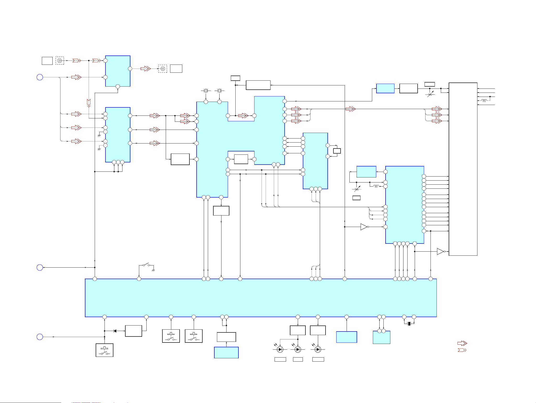
6-1. BLOCK DIAGRAM – MPEG DECODER Section –
B+8V
B+5V
+8V
+5V
HD0 – HD15
DVD MECHANISM
DECK BLOCK
HCS1J
HCS16J
HCS3J
HINTJ
IORDY
ENDSW
HA0
HA1
HA2
IOWJ
IORJ
RST
HDO – HD15
122 – 128,
131 – 137, 140, 141
154
HA0
155
HA1
158
HA2
152
XHCS1FX
151
XHIOCS16
153
HCS3FX
144
HIRQ
146
HIORDY
149
XHWR
150
XHRD
166
ENDSW
145
XHRST
114VBS
113Y
108B-Y
106R-Y
33DAC DATA
39DAC MCLK
40DAC BCK
32DAC LRCK
165DAC ML
143DAC MC
118DAC MD
CVBS
B-Y
R-Y
D/A CONVERTER
2 DATA
16 SCK
1 BCK
3 LRCK
15 ML
14 MC
13 MD
XVM-R90D
CVBS,
Y, B-Y, R-Y
Y
IC7
7VOUTL
8VOUTR
R-CH
11ZEROR
LOW-PASS
FILTER
IC701
MUTING
Q702, 704
MUTING
SWITCH
Q1, 2
R-CH
DELAY
D13, Q3
L-CH_AU
A
B
(Page 19)
(Page 18)
• R-ch is omitted due to same as L-ch.
• SIGNAL PATH
: DVD (VIDEO)
: DVD (AUDIO)
: DIGITAL OUT
: CHECK IN
: CHECK OUT
MS SDIO
MC SCLK
MS BS
MS INS
VCC
VCC
(Page 18)
MEMORY
STICK
DA-BE, CK-BE,
CS-BE
C
B+3.6V
142 MS SDIO
117 MC SCLK
167 MS BS
119 MS INS
DA-BE
DA-BE
CK-BE
CK-BE
168169162
CS-BE
CS-BE
41SPDIF
SDA
160
161
5
4
SDA
EEPROM
IC5
SCL
SCL
OPTICAL
TRANSCEIVER
J301
DB0 - DB15 DMA0 - DMA11 LD0 - LD14 LA0 - LA19
77 - 82, 85 - 90,
93 - 96
2, 4, 5, 7, 8, 10, 11, 13, 42,
44, 45, 47, 48, 50, 51, 53
DQ0 - DQ15 A0 - A11
OPTICAL
OUTPUT
MPEG DECODER
53 - 58,
61 - 66
22 - 26,
29 - 25, 22
SD-RAM
IC6
IC1
102
38
DSCK_EN
DSCK
70
CLK37CKE
DBANK0
73
20
BA021BA1
DBANK1
74
XDCAS72XDRAS0
69
18
17
XCAS
XRAS0
71
16
XDWE
100
19
XWE
XDCS0
DQM
101
39
XCS
DQMH
178 - 182, 185 - 191,
194 - 196
29 - 36, 38 - 44
DQ0 - DQ14
204 - 207, 2-7,
10 - 16, 19 - 21
45, 25, 24 - 16,
8 - 1, 48
A–1, A0 - A18
FLASH ROM
IC3
XLWRLL
198
11
XWE
176
26
XLCS3
170
28
XCE
XLOE
XOE
24XRESET
12XRST
RESET SIGNAL
GENERATOR
IC2
B+5V
XVM-R90D
1717
XVM-R90D
6-2. BLOCK DIAGRAM – AUDIO Section –
RV900
VCO
AUDIO
INPUT
B
(Page 17)
D
(Page 19)
L-CH_AU
SW1
J701 (1/2)
L
R
R-CH
DIFFERENTIAL
AMP
IC703
AUDIO INPUT
1
VIN1
3 VIN2
SELECT
IC704
2
VOUT
SW1
7
R-CH
IR TRANSMITTER
MODULATOR
IC904
ELECTRICAL VOLUME
IC706
8
LIN1
DATA
LOUT1
CLK4DATA
5
CLK
LED DRIVE
Q902
D912, 914, 916
(IR TRANSMITTER)
• R-ch is omitted due to same as L-ch.
• SIGNAL PATH
: DVD (AUDIO)
: AUX INPUT (AUDIO)
LINE AMP
IC708
POWER ON
MUTING
Q321, 322
MUTING
Q708
MUTING
SWITCH
Q318
POWER ON
MUTING
Q319, 320
D911, 913, 915
(IR TRANSMITTER)
MUTING
B+8V
R-CH
MUTING
CONTROL
Q316, 317
Q713
R-CH
DISCHARGE SWITCH
POWER AMP
IC707
STANDBY
SWITCH
Q710, 711
+
Q714, 715
R-CH
R-CH
J702 (1/2)
POWER ON
L
R
SP1
(L)
SP2
(R)
E
AUDIO
OUTPUT
R-CH
7
(Page 20)
C
(Page 17)
DA-BE, CK-BE,
CS-BE
DA-BE
15
16
DA (IN)-BE
CK-BE
CS-BE
17
CK-BE18CS-BE
DA (OUT)-BE
DATA
7
S-SDA
CLK
6
S-SCL
BUFFER
Q206
49
Q207
FM1
R-CH
Q202, 204
RF LEVEL
SWITCHING
Q204
BUFFER
Q205
50
FM2
Q202
R-CH
22
R-CH
B+8V
1
B+ SWITCH
Q323, 324
D317
SYSTEM CONTROLLER
IC401 (1/3)
LIN
RIN
14 13
MPX ADJ
XIN
X201
7.6MHz
5
XOUT
+5V
REGULATOR
IC304
LOW-PASS FILTER
Q208, 209
FM STEREO
MODULATOR
IC201
FM+5V
VTIN
9
PD
7
17
LEVEL SHIFT
Q210 – 213
4
RF OUT
DATA16CLK15CE18ATT
3
5
FM-CE
FM-CLK
FM-DATA
64
AMP ON
BPF
FL201
(FM MODULATOR)
D204
11
53
AMUTE
XVM-R90D
1818
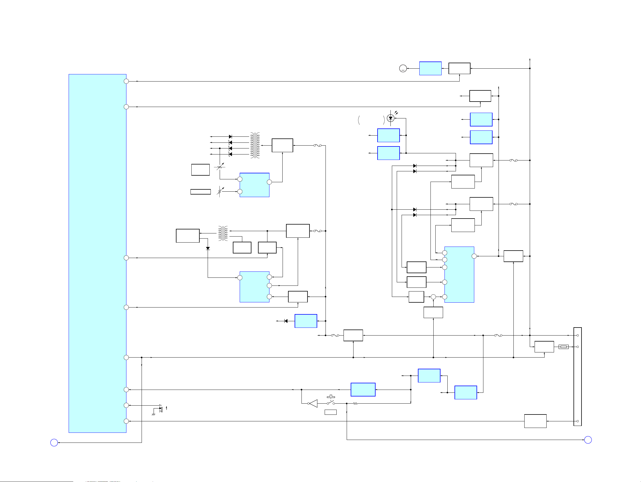
6-3. BLOCK DIAGRAM – VIDEO, PANEL Section –
VIDEO INPUT
SELECT
IC101
6VIN1
4VIN2
SW1
1
VIDEO INPUT SELECT
IC102
1IN1B
16 IN1A
9IN3B
8IN3A
14 IN2B
11 IN2A
SW27SW3
SW1
12
2
2VOUT
3OUT1
6OUT3
5OUT2
S908
(PANEL CLOSE DETECT)
(ON: CLOSE)
30
MONITOR SW
VIDEO
INPUT
A
(Page 17)
D
(Page 18)
CVBS, Y,
B-Y, R-Y
SW1
J701 (2/2)
CVBS
Y
B-Y
R-Y
63
SW1
J702 (2/2)
VIDEO
OUTPUT
SYNC
SEPARATOR
Q502, 503
X501
3.58MHz
VXO-NTSC63VXO-PAL
CTRAPOUT
YIN
52
CIN
57
B-Y IN
5
R-Y IN
4
CSYNCIN
46
CSYNCOUT
V-SDA48V-SCK47HSYNCLOCK
51
52
V-SCK
V-SDA
X502
4.43MHz
64
HDOUT
VDOUT
39
SYNC LOCK
Q505, 506
21
SYNC-DET
TRAP
53
RGB DECODER
34
32
31
IC501
BUFFER
Q501
43
VD
PAL/NTSC SWITCH
Q504
CTRAPIN
54
VDIN
35
HD
VD
SYSTEM CONTROLLER
IC401 (2/3)
VCOMOUT
R-OUT
G-OUT
B-OUT
R-IN2
G-IN2
B-IN2
BLAK36POL
18
BLAK
POL
XVM-R90D
LIQUID CRYSTAL
Q603
DISPLAY MODULE
LCD1
VCOM
VCOM
RED
GREEN
BLUE
STV1
STV2
STH1
STH2
CPH1
CPH2
CPH3
CPV
OEV1
OEV2
OEV3
OEH
L/R
U/D
VHG
VDD1
VCC
VEE
VGH +17V
VDD +3.3V
VCC +5V
VB
VSS –13V
RV802
54
STV1
U/D
V-COM
R
G
B
20
26STV2
23STH1
24STH2
29CPH1
27CPH2
25CPH3
16CPV
19OEV1
18OEV2
17OEV3
21OEH
28L/R
55
LR
V COM AMP
IC802
28
26
21
19
14
15
16
17
YS
R
G
B
OSD DRIVER
IC405
16
VR
17 VG
18 VB
15 BLK
20 HSYNCN
19 YSYNCN
3
DATA
DATA
19
OSC OUT
SCLK2CSN
DATA
1
CLK
CS
CS
CLK
20
22
OSD CSN
OSD SCLK
OSD DATA
7
OSC
8OSC IN
PHASE
COMPARATOR
IC602
RV601
PLL
Q601
23
N/P
HD
VD
BLAK
POL
33
36 VCO1
37 VCO0
2 HSYNCIN
5 VDBIN
8 BLACK
14 POL
46 NP
LCD CONTROLLER
PD
QHSEL31JUST13UD
CPHSEL
4
3
59
58
SIDE1
SIDE2
V COM BIAS
Q803 – 807
IC601
LTBOX
12
57
61
JUST
ZOOM
(Page 20)
XVM-R90D
X2
KEY PW/EJ
29
D402
RESET
F
S902, 903
WAKE UP
SWITCH
Q401, 403
KEY HALT
44
KEY IN
27
S401 – 404
KEY DVD
28
S904 – 907
REM HALT45REM IN
47
SIRCS BUFFER
Q901
REMOTE CONTROL
RECEIVER
IC902
11
LED DRIVE
Q955
POWER EJECT
D901D900
LIGHT PW/EJ
DISC_LED
12
LED DRIVE
Q953
D902
DISC IN
TEMP
33
TEMPERATURE
SENSOR
IC901
SDA13SCL
14
5
SDA
EEPROM
IC402
6
SCL
X1
41 40
X401
4.19MHz
• SIGNAL PATH
: DVD (VIDEO)
: AUX INPUT (VIDEO)
1919
XVM-R90D
6-4. BLOCK DIAGRAM – POWER SUPPLY Section –
FAN CONT
BATT
M301
MM
(FAN)
8
+12V
REGULATOR
IC302
B+SWITCH
Q307, 308
SW12V
SYSTEM CONTROLLER
IC401 (3/3)
IR CONT
DIMMER
TFT ON
PW-ON
CONTROL
Q305, 306
CONTROL
Q302, 303
VCC
B+SWITCH
Q904, 905
+8V
REGULATOR
IC903
+8V
REGULATOR
IC303
SWITCHING
REGULATOR
Q304
SWITCHING
REGULATOR
Q301
9
F950
F302
F301
B+ SWITCH
Q309, 311
B+ SWITCH
Q325, 326
CN301
3
2
BATT
AMP REM
IR LED B+
48
D903
DC/DC
CONVERTER
POWER CONTROL
3
1IN+
2RT
OSC
Q857, 858
POWER CONTROL
1IN+
1
T801
IC801
IC850
71OUT
DIMMER
Q860, 861
162IN+
11
C2
12VCC
VCC +7.5V
DC/DC
CONVERTER
Q801, 802
D950
SWITCHING
REGULATOR
Q855, 856, 859
B+ SWITCH
Q853, 854
+8V
REGULATOR
IC950
VCC
F801
F850
F951
B+ SWITCH
Q951, 952
VSS –13V
VGH +17V
VCC +5V
VDD +3.3V
RV803
5V
VOLTAGE
(DC/DC CONVERTER)
RV801
FREQUENCY
(DC/DC CONVERTER)
INVERTER
TRANSFORMER
BACK LIGHT
UNIT
D852, 853
60
56
2
D801
D802
D803
D804
T850
DISC SLOT
ILLUMINATION
B+2.8V
B+3.6V
SWITCHING
REGULATOR
IC305
SWITCHING
REGULATOR
IC306
D305
D307, 308
D306
D315, 316
DEAD TIME
Q310
DEAD TIME
Q314
LATCH
Q313
+
SWITCHING
Q312
E-VOL +8V
B+5V
B+8V
POWER CONTROL
OUT1
1
10 OUT2
6DT1
11 DT2
15 SCP
IR +8V
REGULATOR
REGULATOR
IC301
XVM-R90D
E
(Page 18)
POWER ON
RESET
ACC Y/N
ACC IN
U-COM +3.3V
36
Q402
31
46
B
S301
(POWER SELECT)
A
S901
RESET
RESET SIGNAL
GENERATOR
IC403
+3.3V
REGULATOR
IC952
PANEL +5V
+5V
REGULATOR
IC951
ACCESSORY
DETECT
Q315
4
RESER
ACC
F
(Page 19)
2020
• Note for Printed Wiring Boards and Schematic Diagrams • Circuit Boards Location
XVM-R90D
Note on Printed Wiring Boards:
• X : parts extracted from the component side.
• Y : parts extracted from the conductor side.
• x : parts mounted on the conductor side.
• : Pattern from the side which enables seeing.
(The other layers' patterns are not indicated.)
Caution:
Pattern face side: Parts on the pattern face side seen from
(Conductor Side) the pattern face are indicated.
Parts face side: Parts on the parts face side seen from
(Component Side) the parts face are indicated.
Caution:
Pattern face side: Parts on the pattern face side seen from
(Side B) the pattern face are indicated.
Parts face side: Parts on the parts face side seen from
(Side A) the parts face are indicated.
Note on Schematic Diagram:
• All capacitors are in µF unless otherwise noted. (p: pF)
50 WV or less are not indicated except for electrolytics
and tantalums.
• All resistors are in Ω and 1/
specified.
• C : panel designation.
• A : B+ Line.
• B : B– Line.
• H : adjustment for repair.
• Power voltage is dc 14.4V and fed with regulated dc power
supply from ACC and BATT cords.
• Voltages and waveforms are dc with respect to ground
under no-signal conditions.
no mark : DVD PLAY
(): STANDBY
∗ : Impossible to measure
• Voltages are taken with a VOM (Input impedance 10 MΩ).
Voltage var iations may be noted due to normal production tolerances.
• Waveforms are taken with a oscilloscope.
Voltage var iations may be noted due to normal production tolerances.
• Circled numbers refer to waveforms.
• Signal path.
L : DVD (VIDEO)
F : DVD (AUDIO)
J : DIGITAL OUT
a : AUX INPUT (VIDEO)
E : AUX INPUT (AUDIO)
d : CHECK IN
G : CHECK OUT
4
W or less unless otherwise
FRONT board
LCD board
JACK (OUT) board
JACK (IN) board
SW board
MAIN board
KEY board
XVM-R90D
2121
XVM-R90D
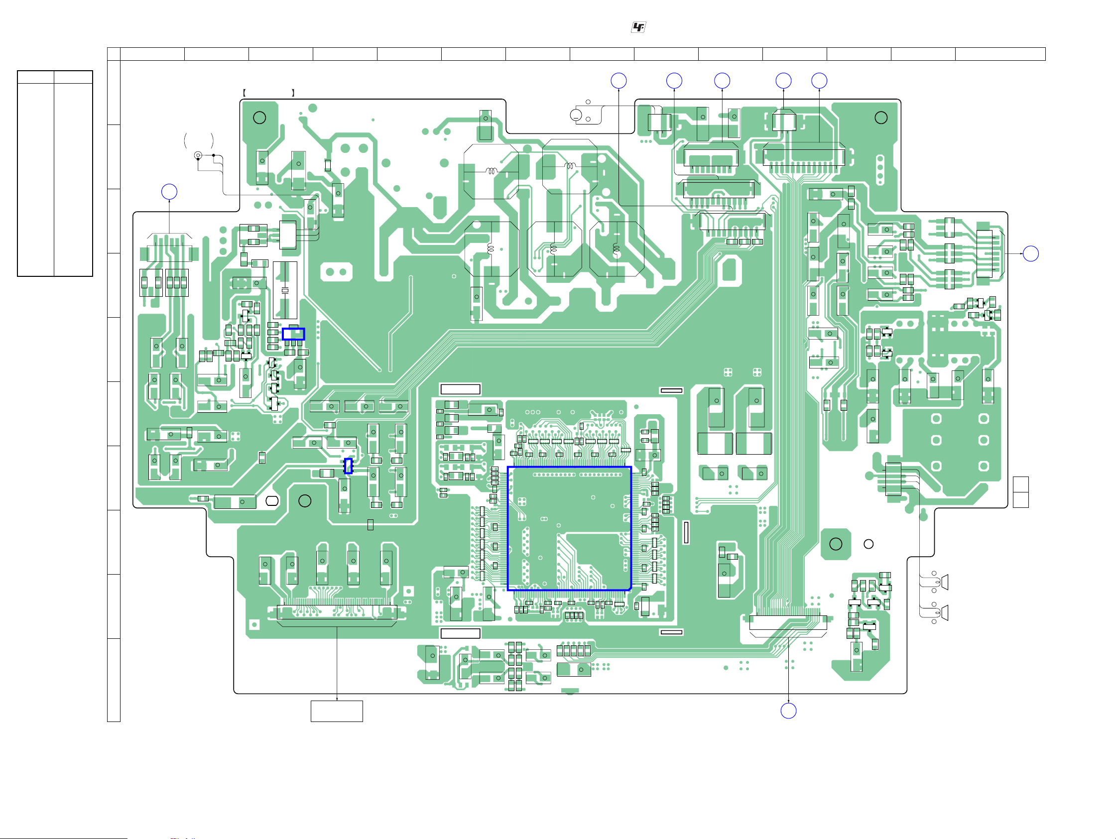
6-5. PRINTED WIRING BOARD – MAIN Board (Component Side) –
• See Page 21 for Circuit Boards Location.
: Uses unleaded solder.
• Semiconductor
Location
Ref. No. Location
D4 I-9
D13 I-12
D204 D-3
D317 F-3
IC1 H-7
IC101 G-4
IC304 E-3
Q1 I-12
Q2 I-12
Q3 I-12
Q205 E-3
Q206 F-3
Q207 E-3
Q208 D-2
Q209 E-3
Q708 E-12
Q709 E-12
Q710 D-14
Q711 D-14
1 2 3 4 5 6 7 8 9 10 11 12 13 14
CN103
(Page 28)
B
C732
+
C736
+
C738
+
C735
+
C744
C743
R730
LCD BOARD
CN906
113
+
+
+
+
R754R755
+
C734
C718
C719
R731
R84
Q3
BCEQ2BCE
R86
R87
R85
R88
+
C150
R83
D13
AKA
C726
C724
C725
C727
R769
R768
+
C745
+
C340
R80
C149
4
1
R775
R774
ECB
Q709
BCE
ECB
Q708
R82
+
+
+
+
CN705
R81
R738
R740
R736
R734
L701
CN701
1
D
R784
7
R785
JACK (IN)
BOARD
CN703
(Page 35)
11
(11)
L702
R735
R737
R741
R739
+
C755
+
C756
L703
R782
+
C757
R781
R783
Q711
Q710
ECB
BCE
+
C759
1-863-445-
+
4
3
Q1
2
1
SP1
(L-CH)
–
+
SP2
(R-CH)
–
(Page 28)
LCD BOARD
CN908
11
2
3
MAIN BOARD
+
C397
A
FM
MODULATOR
ANTENNA
B
(Page 35)
JACK (OUT)
CN704
E
C
61
CN702
R1760
R1761
R1762
D
E
+
C776
+
C772
R1759
L704L705
+
C771
+
C775
R1758
C218
C211
C217
R211
R218
+
+
F
+
C769
+
G
C766
+
C765
R786
R103
C343
C342
+
+
H
I
J
C222
L203
Q208
C215
R217
C165
R214
+
C226
C219
R212
R216
ECB
R236
R235
L202
SGD
+
C220
D204
KA
+
R231R213
C221
R215
Q209
Q205
A
A
C255
+
C367
(COMPONENT SIDE)
+
CN201
3
1
X201
R227
R228
R229
13
R230
C346 C345
BCE
Q207
BCE
Q206
BCE
K
D317
C176
+
C372
150
C362
IC304
+
C344
+
C364
+
C169
L101
+
C370
R105
L307
+
C162
CN101
+
C365
+
IC101
136
+
C166
C170
+
4
C378
+
C254
+
C175
+
C161
C171
+
+
C173
R108R107
+
C168
R106R104
+
C381
C177
C178
C179
C134
C100
+
C95
C384
FB2
FB1
FB3
L1
L3
L4
C147
+
C146
+
1
M301
+
C324
L305
L302
+
C328
+
C22
C23
L51
C96
R70
R31
C31
R32
C99
R72
C34
R34
C35
RB10
RB11
C44C52C58
RB12
RB13
RB14
RB15
+
RB16
156
+
C144
C702
+
C705
C701
R29
R30
+
C72
L56
C30
C33
105
C32
C69
C66
C68
R66
R68
R712
R710
+
+
R704
R703
R709
C704
C703
R711
C710
C711
M
–
(FAN)
L303
C27C28C29
L306
2
R27
RB3RB4RB5RB6RB7RB8
R25
R24
C26
IC1
R44
R43
R42
C74
C71
R40
C103
C104
R75
R76
+
C706
+
C78
C75
C102
C101
R77
R73
R74
+
(Page 28) (Page 28)
LCD BOARD
F C
RB2
C24C25
RB21
CN905
CN302
2
L304
C21
L48
C19
RB1
53104
208157
C82
C17
52
1
D4
+
R21
R20
R19
R12
R9
R8
R7
R5
C4 C7 C18
RB20
RB19
RB18
RB17
C1 C2 C3
AK
LCD BOARD
H
CN907
+
1
C151
C105
C106
C135
C338
CN107
CN105
L314
C392
G
+
C395
+
CN108
R377
+
(Page 35)
SW BOARD
+
C335
18
111
110
R111R110R109
+
C390
L313
+
C386
C383
C382
130
CN104
12
CN102
XVM-R90D
DVD MECHANISM
DECK BLOCK
KEY BOARD
A
CN911
(Page 34)
2222
 Loading...