

Page 1
XVM-F65WL
SERVICE MANUAL
Ver. 1.1 2005.08
• This set consists of the following units.
AEP, UK model US, Canadian model E, Chinese model
MONITOR XVM-F65WL XVM-F65WL XVM-F65WL
CONNECTION BOX XA-126 XA-125 XA-125
REMOTE COMMANDER RM-X709 RM-X709 RM-X709
CORDLESS HEADPHONES —— MV-02HP ——
US Model
Canadian Model
AEP Model
UK Model
E Model
Chinese Model
Monitor XVM-F65WL
System Liquid crystal colour display
Drive system TFT-LCD active matrix system
Picture size 6.5 inches wide screen (16:9)
143.4 × 79.3 mm, 165.1 mm (w/h, d)
Picture segment
280,800 (w 1,200 × h 234) dots
Power requirements
12 V DC car battery (negative ground)
Current drain Approx. 1 A
Dimensions 194 × 101 × 27.1 mm (w/h/d)
(7 3/4 × 4 × 1 1/8 in.)
Operating temperature
0 °C – 45 °C
Mass Approx. 424 g (15 oz)
Connection box XA-126 (AEP, UK model),
XA-125 (US, Canadian, E, Chinese model)
A/V Output
Output Impedance:less than 470 Ω
less than 1,000 pF
Output Level: 0 dBs ±0.3 dB (0.775 V rms)
Video: 75 Ω 1 Vp-p
A/V Input × 2
Input Impedance: more than 10 kΩ
less than 1,000 pF
Input Level (max.):1.3 dBs +0/–0.3 dB (1 V rms)
Video: 75 Ω 1 Vp-p
Dimensions 147.5 × 40 × 80 mm (w/h/d)
(5 7/8 × 1 5/8 × 3 1/4 in.)
Mass Approx. 282 g (10 oz)
SPECIFICATIONS
Card remote commander RM-X709
Power requirements
CR2025 lithium battery
Operable range
Approx. 2.5 m
Dimensions 55 × 125 × 15 mm (w/h/d)
Mass Approx. 40 g
(including batteries)
Headphones (US, Canadian model)
Modulation system
Frequency modulation
Carrier frequency
Right: 2.8 MHz (CH1)/3.8 MHz (CH2)
Left: 2.3 MHz (CH1)/3.2 MHz (CH2)
Frequency response
18 – 22,000 Hz
Power source DC 3.0 V; using R6 dry batteries (2)
Mass Approx. 230 g
(including batteries)
– Continued on next page –
MOBILE MONITOR
9-879-756-02
2005H04-1
© 2005.08
Sony Corporation
e Vehicle Group
Published by Sony Engineering Corporation
Page 2

XVM-F65WL
Ver. 1.1
Supplied accessories
Design and specifications are subject to change
without notice.
Notes on Chip Component Replacement
• Never reuse a disconnected chip component.
• Notice that the minus side of a tantalum capacitor may be damaged
by heat.
UNLEADED SOLDER
•
Boards requiring use of unleaded solder are printed with the leadfree mark (LF) indicating the solder contains no lead.
(Caution: Some printed circuit boards may not come printed with
Installation kit (1)
Monitor stand (1) (AEP, UK, E, Chinese model)
(with supplied screws (5))
Connection box XA-126 (1) (AEP, UK model)
Connection box XA-125 (1)
(US, Canadian, E, Chinese model)
Cordless headphones MV-02HP (1)
(US, Canadian model)
Rechargeable battery MV-100BAT (1)
(AEP, UK, E, Chinese model)
Battery rechargeable cable (1)
(AEP, UK, E, Chinese model)
Card remote commander RM-X709
(with supplied battery) (1)
Power supply cord (1)
Detach cradle (3 m) (1)
Cigar plug (0.3 m) (1)
Operating Instructions (1 set)
the lead free mark due to their particular size.)
: LEAD FREE MARK
Unleaded solder has the following characteristics.
• Unleaded solder melts at a temperature about 40°C higher than
ordinary solder.
Ordinary soldering irons can be used but the iron tip has to be
applied to the solder joint for a slightly longer time.
Soldering irons using a temperature regulator should be set to
about 350°C.
Caution: The printed pattern (copper foil) may peel away if the
heated tip is applied for too long, so be careful!
• Strong viscosity
Unleaded solder is more viscous (sticky, less prone to flow)
than ordinary solder so use caution not to let solder bridges
occur such as on IC pins, etc.
• Usable with ordinary solder
It is best to use only unleaded solder but unleaded solder may
also be added to ordinary solder.
SAFETY-RELATED COMPONENT WARNING!!
COMPONENTS IDENTIFIED BY MARK 0 OR DOTTED LINE
WITH MARK 0 ON THE SCHEMATIC DIAGRAMS AND IN
THE PARTS LIST ARE CRITICAL TO SAFE OPERATION.
REPLACE THESE COMPONENTS WITH SONY PARTS WHOSE
PA RT NUMBERS APPEAR AS SHOWN IN THIS MANUAL OR
IN SUPPLEMENTS PUBLISHED BY SONY.
TABLE OF CONTENTS
1. SERVICING NOTES ................................................ 3
2. GENERAL
Location of Controls ........................................................ 4
Connections ..................................................................... 6
3. DISASSEMBLY
3-1. Cabinet (Rear) Assy ......................................................... 9
3-2. Monitor Board ................................................................. 9
3-3. LCD1 ............................................................................... 10
4. TEST MODE ............................................................... 11
5. ELECTRICAL ADJUSTMENTS
5-1. Equipment Used .............................................................. 12
5-2. Connection of Equipment ................................................ 12
5-3. Setup for Adjustment....................................................... 12
5-4. DC-DC Converter Adjustment ........................................ 12
5-4-1. Frequency Adjustment ............................................. 12
5-4-2. 5V Voltage Adjustment ............................................ 12
5-4-3. Other Voltage Checks ............................................... 12
5-5. PLL Adjustment .............................................................. 12
5-6. Inverter High Voltage Check ........................................... 13
5-6-1. Voltage Check .......................................................... 13
5-6-2. Frequency Check ..................................................... 13
5-7. OSD Dot Clock Check .................................................... 13
5-8. NTSC Subcarrier Check .................................................. 13
5-9. PAL Subcarrier Check ..................................................... 13
5-10. F0 Frequency Adjustment ............................................... 13
5-10-1. 3.2/3.8 MHz (CH2) Adjustment ............................ 13
5-10-2. 2.3/2.8 MHz (CH1) Check ..................................... 13
5-11. V COM Voltage/Position Adjustment ............................. 13
5-12. Video Adjustment ............................................................ 14
5-12-1. Brightness Signal Contrast Level (Y GAIN) ......... 14
5-12-2. Black Limiter Level Adjustment ............................ 14
5-12-3. White Limiter Level Adjustment ........................... 14
5-12-4. R Sub Brightness Adjustment ................................ 14
5-12-5. B Sub Brightness Adjustment ................................ 14
5-12-6. R Sub Contrast Adjustment ................................... 14
5-12-7. B Sub Contrast Adjustment ................................... 15
5-12-8. γ 1 Adjustment ....................................................... 15
5-12-9. γ 2 Adjustment ....................................................... 15
5-12-10. VCO Free Run Adjustment .................................... 15
5-12-11. V POS Adjustment ................................................. 15
5-12-12. H POS Adjustment................................................. 15
6. DIAGRAMS
6-1. Block Diagram –Connection Box Section– .................... 17
6-2. Block Diagram –Video Section– ..................................... 18
6-3. Block Diagram –Display Section– .................................. 19
6-4. Printed Wiring Board –Connection Box Section– .......... 22
6-5. Schematic Diagram –Connection Box Section (1/2)– .... 24
6-6. Schematic Diagram –Connection Box Section (2/2)– .... 25
6-7. Printed Wiring Boards –Monitor Section– ...................... 26
6-8. Schematic Diagram –Monitor Section (1/4)– ................. 28
6-9. Schematic Diagram –Monitor Section (2/4)– ................. 29
6-10. Schematic Diagram –Monitor Section (3/4)– ................. 30
6-11. Schematic Diagram –Monitor Section (4/4)– ................. 31
7. EXPLODED VIEWS
7-1. Cabinet (Rear) Section .................................................... 38
7-2. Cabinet (Front) Section ................................................... 39
7-3. Connection Box Unit ....................................................... 40
7-4. Cradle Section ................................................................. 41
8. ELECTRICAL PARTS LIST .................................. 42
2
Page 3
SECTION 1
SERVICE NOTES
NOTE FOR REPLACEMENT OF THE EEP ROM (IC403)
The EEP ROM (IC403) contains all data by which the LCD screen is defined.
When the EEP ROM is replaced, the normal LCD screen will not appear.
It is then necessary to write the data into the EEP ROM.
Writing Method:
1. Turn on power to the connection box XA-125/126.
2. Press the [POWER] key on the set to turn on the set.
(Normal LCD screen doesn’t appear because there is no data in EEP ROM.)
3. Press the [RESET] key while pressing the [INPUT] and [VOL--] keys on the set.
4. Press the [VOL--] key on the remote controller for more than 2 seconds.
5. The EEP ROM data will be written and the normal test mode screen will appear.
After this, perform V COM voltage/position adjustment as well as VIDEO adjustment.
NOTE FOR REPLACEMENT OF THE SYSTEM CONTROL (IC401)
When the IC401 is replaced, the video system should be set again according to the destinations.
XVM-F65WL
Ver. 1.1
Setting Method:
1. Enter the test mode. (See page 11).
2. Select NTSC/PAL SELECT from the test mode menu.
3. Set the video system to the appropriate mode for each destination by using the [MENU] key.
Video mode Destination
NTSC 2.4G PACK US, Canadian
PAL 2.4G PACK E, Chinese
PAL RGB 2.4G PACK AEP, UK
3
Page 4
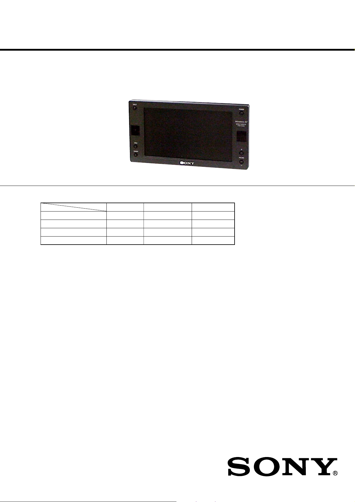
XVM-F65WL
Location of controls
Monitor
15
2
SECTION 2
GENERAL
This section is extracted
from instruction manual.
7 8
1 INPUT button
Press to select the input source.
2 Receptor for the card remote
commander/Transmitter for the
cordless headphones*
3 MENU button
Press to make various settings.
4 DIMMER button
Press to switch the dimmer on/off.
(When it is set to On, the display
darkens.)
5 POWER (on/off) button
Press to turn on/off the monitor.
*
If interference occurs while using several cordless headphones
If several monitors are installed and used simultaneously, interference may occur.
6
43
6 VOLUME +/– buttons
Press to turn up or down the volume
(The default volume level is 25.) or
to select the item during menu
operation.
7
RESET button
8 Monaural speaker
6
4
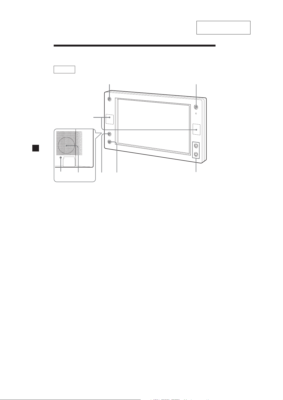
Page 5
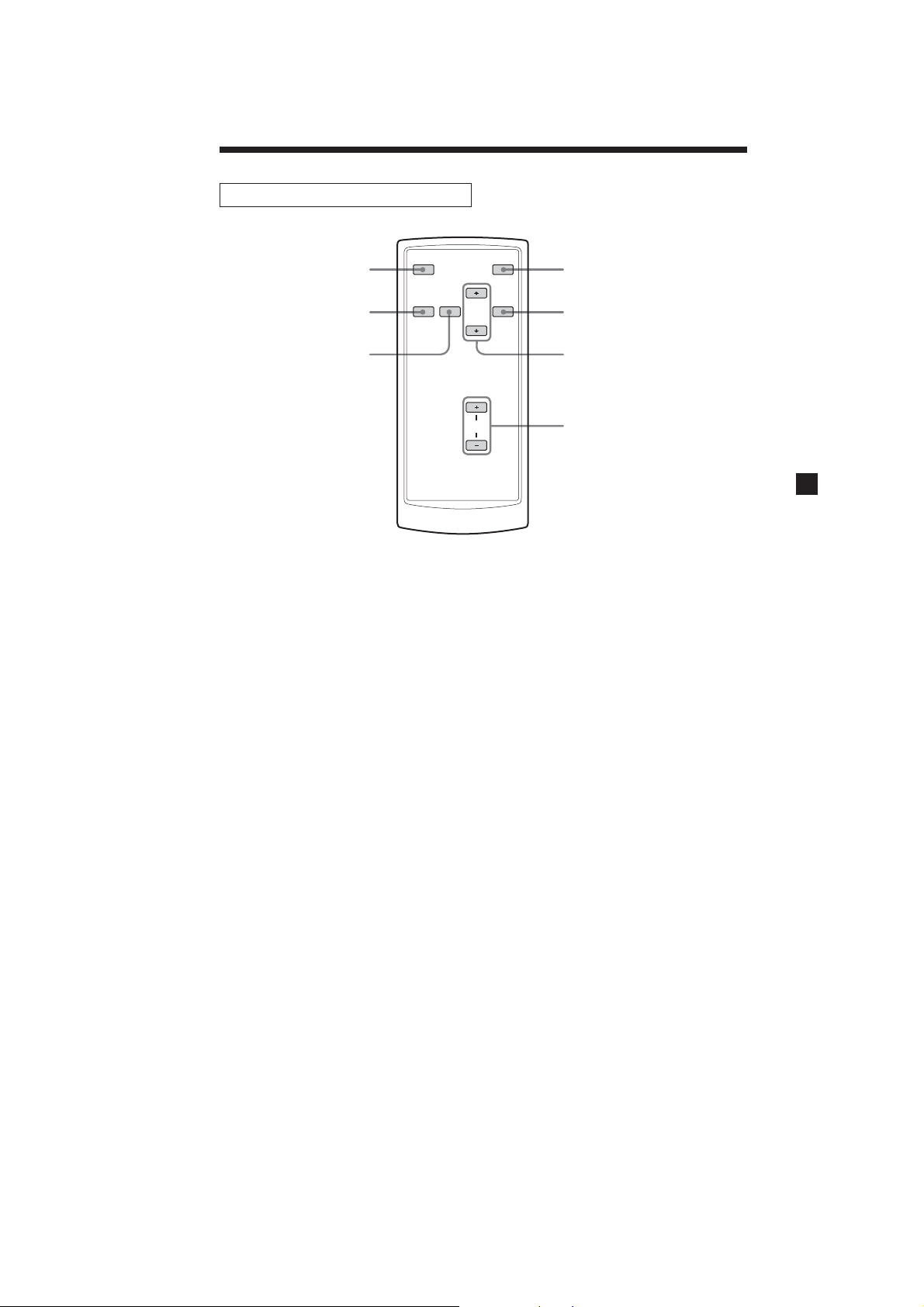
Card remote commander RM-X709
XVM-F65WL
1
2
3
1 ATT button
Press to quickly attenuate the
volume.
To restore the previous volume
level, press (ATT) again or (VOL)
+/–.
2 INPUT button
Press to select the input source.
3 MENU button
Press to select the menu settings.
4 |/1 (power) button
INPUT
AT T
`/1
4
MODEMENU
5
6
VOL
5 MODE button
6 M/m buttons
7 VOL (volume) +/– buttons
7
Press to change the screen mode.
Press to select the desired item.
Press to adjust the volume of the
monitor.
Tip
Refer to “Replacing the lithium battery” for details on how to replace the batteries (page 19).
7
5
Page 6
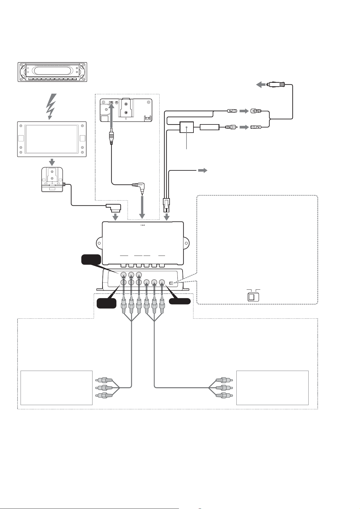
XVM-F65WL
Connections
US, Canadian model
MEX-R5 (optional)
MEX-R5 (en option)
XVM-F65WL
2
Installation cradle
Berceau d’installation
INPUT
VIDEO 1
5
To charge the
rechargeable battery
Pour charger la pile
rechargeable
MV-100BAT
(optional)
MV-100BAT
(en option)
Battery
rechargeable
cable (Supplied)
Câble de pile
rechargeable
(en option)
3
MONITOR
(XVM)
INPUT
VIDEO 1
VIDEO 2
RGB
VLR VLR
DC OUT 9V
MAX 7A
OUTPUT
POWER
DC 12V 3A
REAR/FRONT
Black
Noir
Red
Rouge
LOCATION
1
Blue
Bleu
LC filter
Filtre LC
Cigar lighter adaptor (supplied)
Adaptateur d’allume-cigare (fourni)
To the cigar lighter socket
A la douille d’allume-cigare
Fuse (4 A)
Fusible (4 A)
To the parking brake switch cord
Au cordon du commutateur du frein de stationnement
Switch the location you mount the monitor
To use the monitor on dashboard:
Switch to “FRONT” and connect the blue cord to the parking
brake.
To use the monitor behind the headrest:
Switch to “REAR”.
Commutez l’emplacement de montage du moniteur
Pour utiliser le moniteur sur le tableau de bord:
Commutez à « FRONT » et connectez le cordon bleu au frein de
stationnement.
Pour utiliser le moniteur derrière le repose-tête:
Commutez à « REAR ».
4
RCA cable (not supplied)
Câble RCA (non fourni)
From DVD player
Du lecteur DVD
Notes
• Be sure to connect the power input cord after all
other cords have been connected.
• Be sure to insert each connector securely, as
vibration through driving may cause a poor
connection.
• When removing the cable, hold the connector to
avoid damages.
VIDEO 2
RCA cable (not supplied)
Câble RCA (non fourni)
Remarques
• Connectez bien le cordon d’entrée d’alimentation
après le raccordement de tous les autres cordons.
•Insérez fermement tous les connecteurs, car la
vibration due à la conduite peut provoquer une
mauvaise connexion.
•Au retrait du câble, saisissez le connecteur pour
éviter les dommages.
REAR FRONT
OUTPUTINPUT
To ot her monitor
A un autre moniteur
6
Page 7
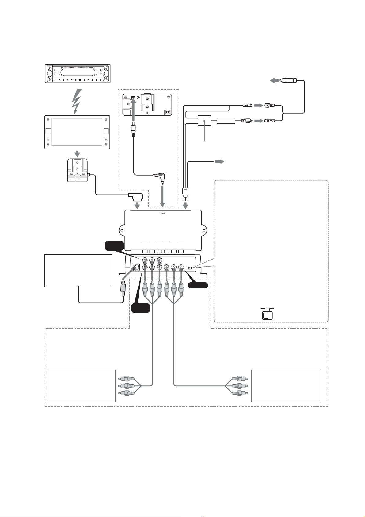
Connections
AEP, UK model
MEX-R5 (optional)
MEX-R5 (en option)
MEX-R5 (optional)
To charge the rechargeable battery
Pour charger la pile rechargeable
Zum Aufladen des Akkus
Black
Noir
Schwarz
Cigar lighter adaptor (supplied)
Adaptateur d’allume-cigare (fourni)
Zigarettenanzünderadapter (mitgeliefert)
To the cigar lighter socket
A la douille d’allume-cigare
An Zigarettenanzünderbuchse
XVM-F65WL
XVM-F65WL
3
Installation cradle
Berceau d’installation
Einbauhalterung
Navigation system etc.
Système de navigation etc.
Navigationssystem usw.
INPUT
VIDEO 1
6
MV-100BAT
Battery rechargeable
cable (supplied)
Câble de pile
rechargeable (fourni)
Akkuladekabel
(mitgeliefert)
4
MONITOR
(XVM)
RGB
DC OUT 9V
MAX 7A
INPUT
VIDEO 1
VIDEO 2
VLR VLR
1
OUTPUT
POWER
DC 12V 3A
REAR/FRONT
Red
Rouge
Rot
LOCATION
Blue
Bleu
Blau
2
OUTPUT
LC filter
Filtre LC
LC-Filter
Fuse (4 A)
Fusible (4 A)
Sicherung (4 A)
To the parking brake switch cord
Au cordon du commutateur du frein de stationnement
An Feststellbremsen-Schalterkabel
Switch the location you mount the monitor
To use the monitor on dashboard:
Switch to “FRONT” and connect the blue cord to the parking
brake.
To use the monitor behind the headrest:
Switch to “REAR”.
Commutez l’emplacement de montage du moniteur
Pour utiliser le moniteur sur le tableau de bord:
Commutez à « FRONT » et connectez le cordon bleu au frein de
stationnement.
Pour utiliser le moniteur derrière le repose-tête:
Commutez à « REAR ».
Andere Einbaustelle für den Monitor wählen
Zur Verwendung des Monitors auf dem Armaturenbrett:
Schalten Sie auf „FRONT“ und schließen Sie das blaue Kabel an
die Feststellbremse an.
Zur Verwendung des Monitors hinter der Kopfstützt:
Schalten Sie auf „REAR“.
RGB cable (not supplied)
Câble RGB (non fourni)
RGB-Kabel (nicht mitgeliefert)
RCA cable (not supplied)
Câble RCA (non fourni)
RCA-Kabel (nicht mitgeliefert)
From DVD player
Du lecteur DVD
Von DVD-Player
Notes
• Be sure to connect the power input cord after all
other cords have been connected.
• Be sure to insert each connector securely, as
vibration through driving may cause a poor
connection.
•When removing the cable, hold the connector to
avoid damages.
•When connecting the additional monitor, even if
you select “NAVI” for the input source, the audio
of the additional monitor or the cordless
headphone will be “VIDEO 1”.
• Please use the commercially available RGB cable
with the connector that fits the RGB jack of the
connection box.
INPUT
VIDEO 2
RCA cable (not supplied)
Câble RCA (non fourni)
RCA-Kabel (nicht mitgeliefert)
Remarques
• Connectez bien le cordon d’entrée d’alimentation
après le raccordement de tous les autres cordons.
• Insérez fermement tous les connecteurs, car la
vibration due à la conduite peut provoquer une
mauvaise connexion.
•Au retrait du câble, saisissez le connecteur pour
éviter les dommages.
•Au raccordement d’un moniteur additionnel,
même si vous sélectionnez « NAVI » comme source
d’entrée, le son du moniteur additionnel ou du
casque sans fil sera « VIDEO 1 ».
• Utilisez un câble RGB disponible dans le commerce
avec connecteur adapté à la prise RGB de la boîte
de raccordement.
REAR FRONT
To o t her monitor
A un autre moniteur
An anderen Monitor
Hinweise
• Schließen Sie das Stromeingangskabel erst an,
nachdem alle anderen Kabel angeschlossen sind.
• Stellen Sie sicher, jeden Stecker fest anzuschließen,
da Fahrvibrationen die Verbindungen lockern
können.
• Beim Abnehmen des Kabels greifen Sie am Stecker,
um Schäden zu vermeiden.
• Beim Anschließen des zusätzlichen Monitors ist
das Tonsignal des zusätzlichen Monitors oder
schnurlosen Kopfhörers „VIDEO 1“, auch wenn Sie
„NAVI“ als Eingangsquelle wählen.
• Bitte verwenden Sie ein handelsübliches RGBKabel mit passendem Stecker für die RGB-Buchse
an der Anschlussbox.
7
Page 8

XVM-F65WL
SECTION 3
DISASSEMBLY
Note: This set can be disassemble according to the following sequence.
SET
3-1. CABINET (REAR) ASSY
(Page 9)
3-2. MONITOR BOARD
(Page 9)
3-3. LCD1
(Page 10)
8
Page 9
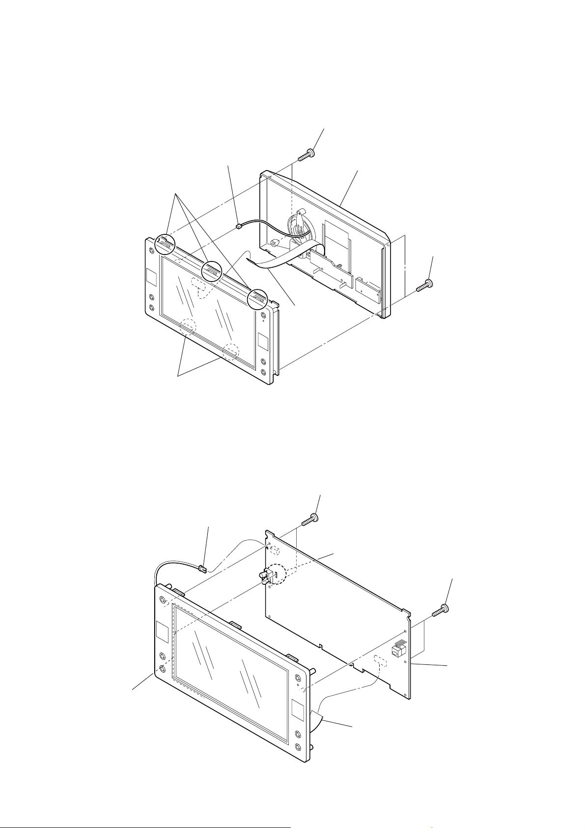
Note: Follow the disassembly procedure in the numerical order given.
s
3-1. CABINET (REAR) ASSY
6
CN252
3
three claws
2
two screws
(+P 2 × 8)
7
cabinet (rear) assy
1
two screw
(+P 2 × 8)
XVM-F65WL
3-2. MONITOR BOARD
4
two claws
2
CN801
5
CN904
4
two screws
(+BTP 2 × 6)
5
Remove the solder.
3
two screws
(+BTP 2 × 6)
bracket (LCD)
6
MONITOR board
1
CN701
9
Page 10
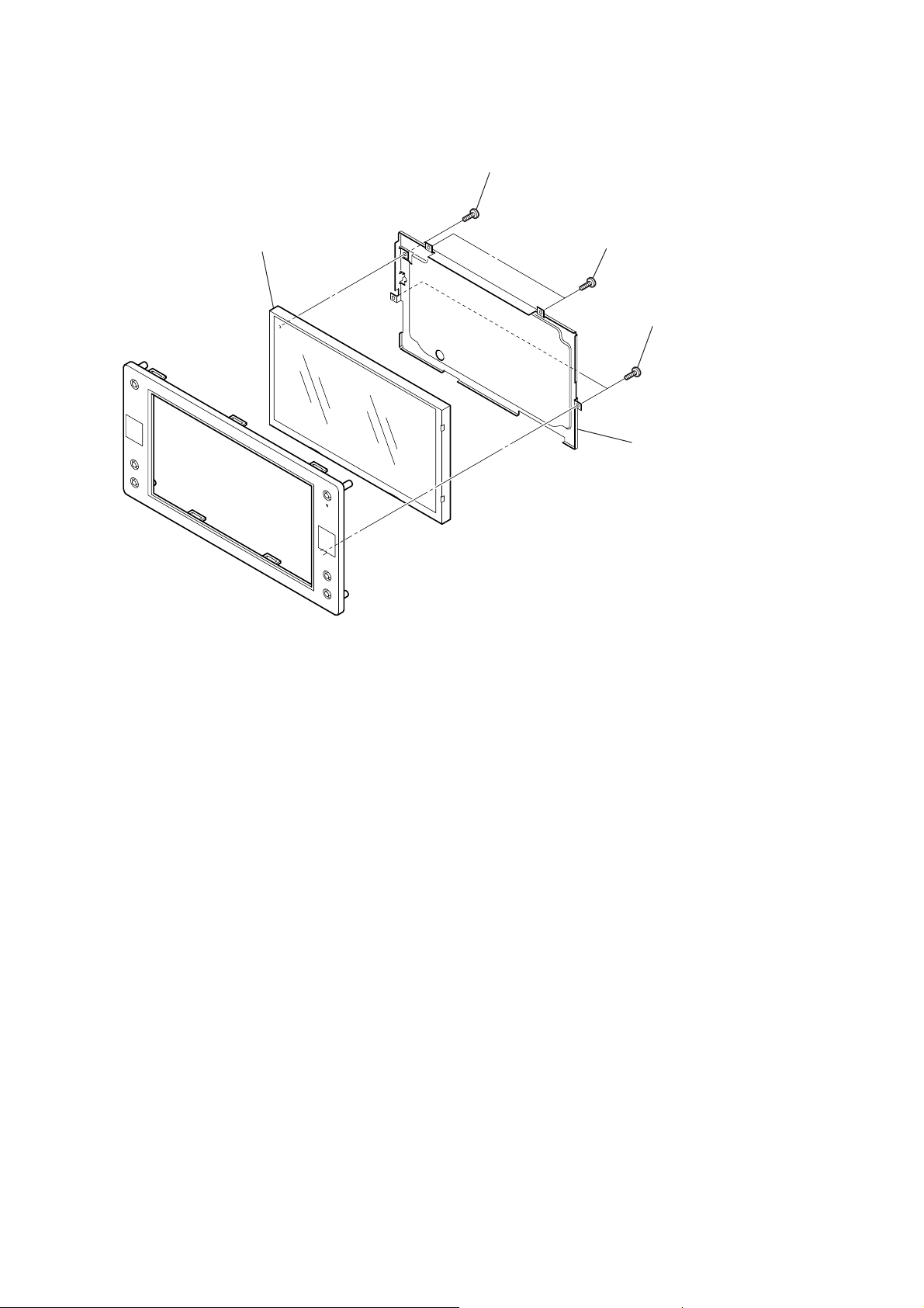
XVM-F65WL
3-3. LCD1
5
LCD1
3
precision screw
(+P 1.7 × 1.8)
1
two screws
(+BTP 2 × 6)
4
2
two screws
(+BTP 2 × 6)
bracket (LCD)
10
Page 11

SECTION 4
TEST MODE
Setting Method:
1. Turn on power to the connection box XA-125/126.
2. Press the [POWER] key on the set to turn on the set.
3. Press the [RESET] key while pressing the [INPUT] and [VOL--]
Keys on the set. Then TEST MODE MENU appears.
Terminating Method:
Select the MENU No. 5, SOFT RESET using the [MENU] key on
the remote controller and determine the selection using the [INPUT]
key.
The FOR FACTORY Mode:
The FOR FACTORY mode can be used to perform 13 different
adjustment items with the remote controller.
1. Select the MENU No. 2, FOR FACTORY using the [MENU] key
on the remote controller and determine the selection using the
[INPUT] key.
2. The FOR FACTORY mode is now entered. The following items
are selected in turn by pressing the [INPUT] key repeatedly.
XVM-F65WL
Com Gain
Y Gain
Black Limt
White Limt
R SUB BRT
B SUB BRT
R SUB CONT
B SUB CONT
Gamma1
Gamma2
VCO Free Run
PLL/V Pos
H Pos
3. For each item selected, adjust so that the adjustment value is
within the specified value range using the R and r keys on the
remote controller.
4. After adjustment, press the [INPUT] key on the remote controller
to determine the adjustment value. After that, it changes into the
following item.
5. After all necessary adjustments are completed, select EXIT
using the [MENU] key on the remote controller and press the
[INPUT] key to display the MENU screen. Then, select No.5,
SOFT RESET using the [MENU] key and determine the selection
using the [INPUT] key to terminate the TEST mode.
11
Page 12
XVM-F65WL
y
SECTION 5
ELECTRICAL ADJUSTMENTS
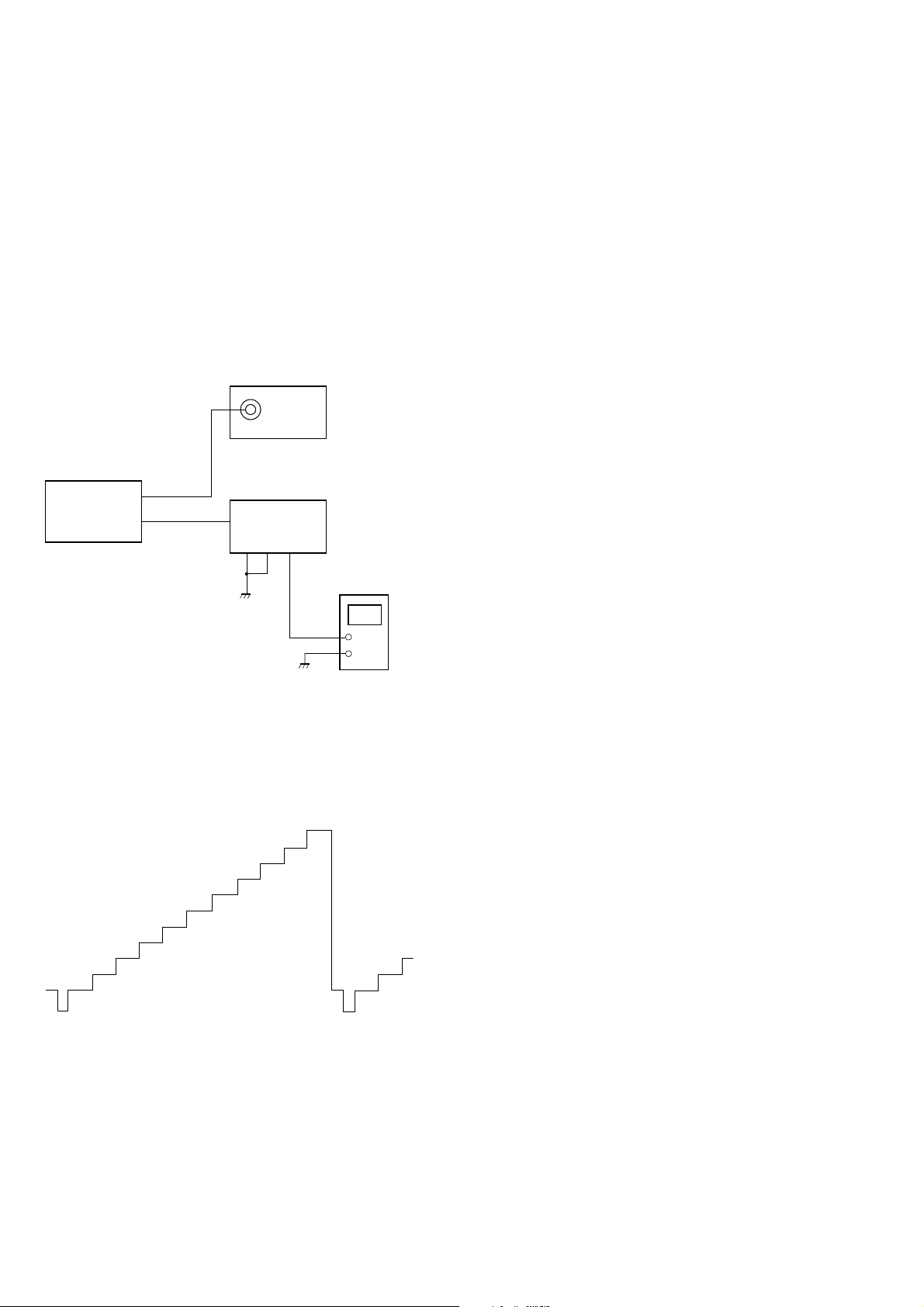
5-1. EQUIPMENT USED
The following measuring equipment are used for these electrical
adjustments:
• Oscilloscope
• NTSC pattern generator
• Stabilized power supply
• Digital voltmeter
• Frequency counter
5-2. CONNECTION OF EQUIPMENT
Unless otherwise specified, the equipment should be connected as
shown below.
NTSC pattern
generator
VIDEO OUT
(75 Ω)
monitor
XVM-F65WL
MONITOR
board
TP501(+)
TP502(–)
connection box
XA-125/126
GND
PARK
BATT
stabilized
power suppl
14.4 V
5-3. SETUP FOR ADJUSTMENT
The 10-step gray scale signal from the NTSC pattern generator is
used as an adjustment signal for V COM voltage/position adjustment
as well as VIDEO adjustment.
5-4. DC-DC CONVERTER ADJUSTMENT
5-4-1. Frequency Adjustment
Adjustment Method:
1) Connect frequency counter between TP702 (+) and TP704 (–).
2) Adjust RV702 so that the reading on the counter stands at the
specified value.
Specified value: 243 ± 3 kHz
Adjustment location: Monitor board
5-4-2. 5V Voltage Adjustment
Adjustment Method:
1) Connect digital voltmeter between TP707 (+) and TP710 (–).
2) Adjust RV701 so that the reading on the voltmeter stands at the
specified value.
Specified value: 5.05 ± 0.03 V
Adjustment location: Monitor board
5-4-3. Other Voltage Checks
Checking Method:
1) Connect digital voltmeter between TP708 (+) (Vdd) and
TP710 (–).
2) Verify that the reading on the voltmeter is at 3.20 ± 0.2 V.
3) Connect digital voltmeter between TP706 (+) (Vgh) and
TP710 (–).
4) Verify that the reading on the voltmeter is at 7.3 ± 0.3 V.
5) Connect digital voltmeter between TP705 (+) (Vgh) and
TP710 (–).
6) Verify that the reading on the voltmeter is at 17.0 ± 1.5 V.
7) Connect digital voltmeter between TP709 (+) (Vss) and
TP710 (–).
8) Verify that the reading on the voltmeter is at –12.0 ± 1.5 V.
Checking location: Monitor board
5-5. PLL ADJUSTMENT
1. Frequency Adjustment
Adjustment Method:
1) Connect digital voltmeter between TP651 (+) and TP652 (–).
2) Adjust RV651 so that the reading on the voltmeter stands at the
specified value.
10-step gray scale signal (with burst), 1Vp-p, 75 Ω
12
Specified value: 2.2 ± 0.15 V
Adjustment location: Monitor board
Page 13
XVM-F65WL
C
B
0V
A
5-6. INVERTER HIGH VOLTAGE CHECK
Condition: DIMMER switch OFF
5-6-1. Voltage Check
Checking Method:
1) Connect oscilloscope between TP809 (+) and TP804 (–) using
high voltage proof probes (100:1).
2) Verify that the reading on the oscilloscope is at 2.4 ± 0.15 Vpp.
Checking location: Monitor board
5-6-2. Frequency Check
Checking Method:
1) Connect oscilloscope between TP809 (+) and TP804 (–) using
high voltage proof probes.
2) Verify that the reading on the oscilloscope is at 50 ± 2.5 kHz.
Checking location: Monitor board
5-7. OSD DOT CLOCK CHECK
1. Dot Clock Check
Checking Method:
1) Connect frequency counter between TP555 (+) and TP554 (–).
2) Verify that the reading on the counter is at 6.5 ± 0.2 MHz.
Checking location: Monitor board
5-8. NTSC SUBCARRIER CHECK.
1. Subcarrier Check
Checking Method:
1) Press the [INPUT] key on the remote controller and enter the
NTSC mode using the R and r keys.
2) Connect frequency counter between TP503 (+) and TP504 (–).
3) Verify that the reading on the counter is at 3.579545 MHz ± 100
Hz.
Checking location: Monitor board
5-9. PAL SUBCARRIER CHECK
1. Subcarrier Check
Checking Method:
1) Press the [INPUT] key on the remote controller and enter the
PAL mode using the R and r keys.
2) Connect frequency counter between TP503 (+) and TP504 (–).
3) Verify that the reading on the counter is at 4.433619 MHz ± 100
Hz.
Checking location: Monitor board
5-10. F0 FREQUENCY ADJUSTMENT
5-10-1. 3.2/3.8MHz (CH2) Adjustment
Adjustment Method:
LCH (3.2 MHz)
1) TP356 is connected to GND.
2) Connect frequency counter between TP354 (+) and TP353 (–).
3) Adjust RV352 so that the reading on the counter stands at the
specified value.
Specified value: 3.2 MHz ± 3 kHz
RCH (3.8 MHz)
4) Connect frequency counter between TP352 (+) and TP353 (–).
5) Adjust RV351 so that the reading on the counter stands at the
specified value.
Specified value: 3.8 MHz ± 3 kHz
Adjustment location: Monitor board
5-10-2. 2.3/2.8MHz (CH1) Check
Checking Method:
LCH (2.3MHz)
1) TP365 is made open.
2) Connect frequency counter between TP354 (+) and TP353 (–).
3) Verify that the reading on the counter is at 2.3 MHz ± 30 kHz.
RCH (2.8MHz)
4) Connect frequency counter between TP352 (+) and TP353 (–).
5) Verify that the reading on the counter is at 2.8 MHz ± 30 kHz.
Checking location: Monitor board
5-11. V COM VOLTAGE/POSITION ADJUSTMENT
Condition: TEST MODE (See 11 page)
1. Voltage Setup Adjustment
Adjustment method:
1) Select Com Gain from the FOR FACTORY MODE.
2) Connect oscilloscope between TP724 (+) and TP710 (–).
3) Adjust so that the p-p value A of the waveform stands at the
specified value using the R and r keys on the remote controller.
4) Adjust so that the level B on the negative side stands at the
specified value using RV652.
5) Verify that the level C on the positive side stands at the specified
value.
Specified value A: 6.8 ± 0.1 Vp-p
Specified value B: –2.1 ± 0.1 V
Specified value C: 4.7 ± 0.1 V
Adjusting location: Monitor board
13
Page 14
XVM-F65WL
5-12. VIDEO ADJUSTMENT
Conditions: TEST MODE (See 11 page)
10-step gray scale signal input
NTSC mode
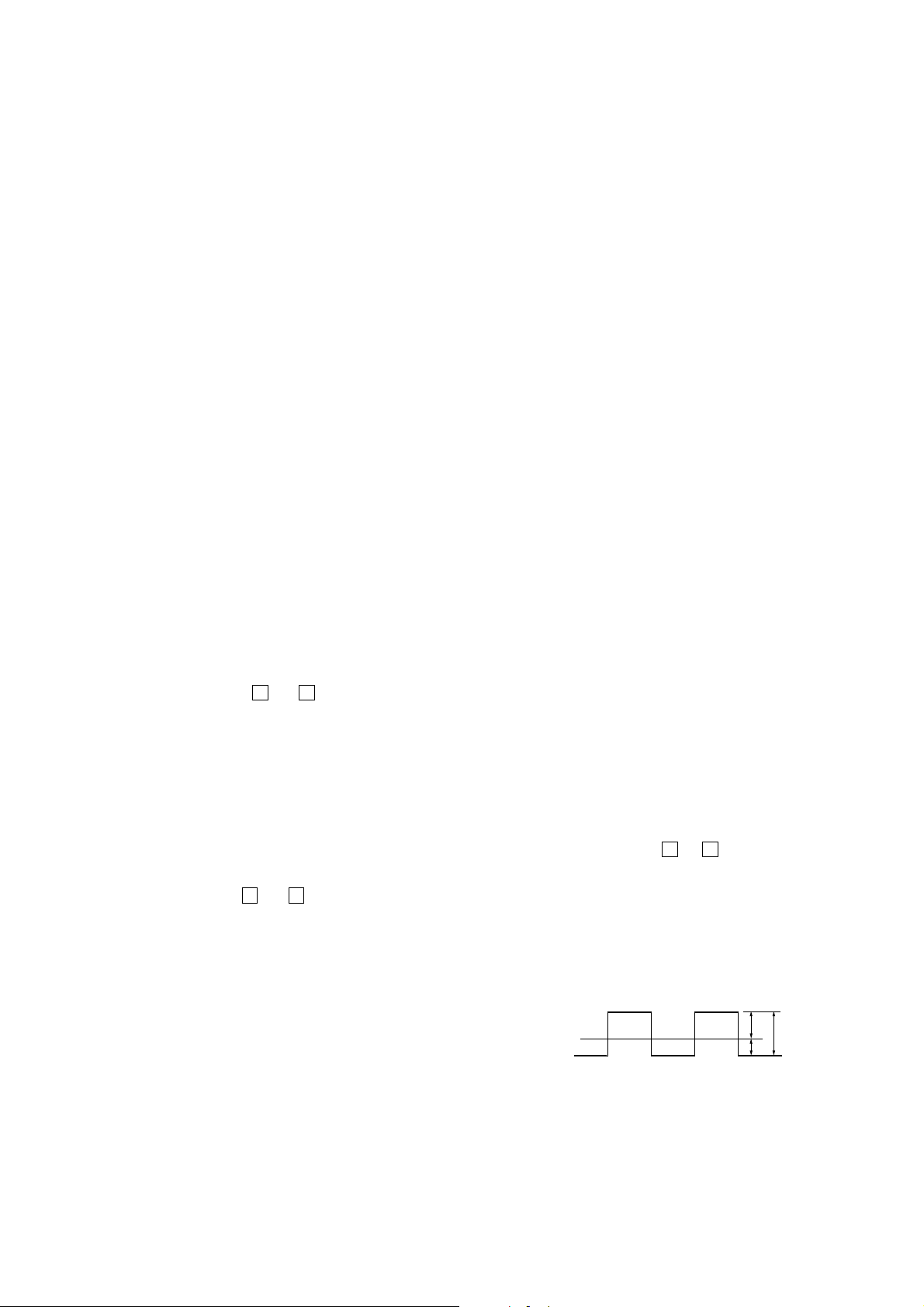
5-12-1. Brightness Signal Contrast Level (Y GAIN)
Adjustment Method:
1) Select Y Gain from the FOR FACTORY MODE.
2) Connect oscilloscope between TP714 (+) and TP710 (–).
3) Adjust so that the signal level A stands at the specified value
using the
Specified value: 3.8 ± 0.1 V
Adjustment location: Monitor board
5-12-2. Black Limiter Level Adjustment
Adjustment Method:
1) Select Black Limit from the FOR FACTORY MODE.
2) Connect oscilloscope between TP714 (+) and TP710 (–).
3) Adjust so that the signal level B stands at the specified value
using the
R
and r keys on the remote controller.
A
R
and r keys on the remote controller.
0V
5-12-4. R Sub Brightness Adjustment
Adjustment Method:
1) Select R SUS BRT from the FOR FACTORY MODE.
2) Connect oscilloscope between TP713 (+) and TP710 (–).
3) Adjust so that the signal level D stands at the specified value
R
using the
and r keys on the remote controller.
Specified value: 1.05 ± 0.15 V
D
0V
Adjustment location: Monitor board
5-12-5. B Sub Brightness Adjustment
Adjustment Method:
1) Select B SUS BRT from the FOR FACTORY MODE.
2) Connect oscilloscope between TP715 (+) and TP710 (–).
3) Adjust so that the signal level E stands at the specified value
R
using the
and r keys on the remote controller.
Specified value: 1.05 ± 0.15 V
Specified value: 1.05 ± 0.15 V
B
0V
Adjustment location: Monitor board
5-12-3. White Limiter Level Adjustment
Adjustment Method:
1) Select White Limit from the FOR FACTORY MODE.
2) Connect oscilloscope between TP714 (+) and TP710 (–).
3) Adjust so that the signal level C stands at the specified value
R
using the
and r keys on the remote controller.
Specified value: 3.95 ± 0.15 V
C
E
0V
Adjustment location: Monitor board
5-12-6. R Sub Contrast Adjustment
Adjustment Method:
1) Select R SUB CONT from the FOR FACTORY MODE.
2) Connect oscilloscope between TP713 (+) and TP710 (–).
3) Adjust so that the signal level F stands at the specified value
R
using the
and r keys on the remote controller.
Specified value: 3.8 ± 0.1 V
F
0V
Adjustment location: Monitor board
Adjustment location: Monitor board
14
0V
Page 15
XVM-F65WL
5-12-7. B Sub Contrast Adjustment
Adjustment Method:
1) Select B SUB CONT from the FOR FACTORY MODE.
2) Connect oscilloscope between TP715 (+) and TP710 (–).
3) Adjust so that the signal level G stands at the specified value
using the R and r keys on the remote controller.
Specified value: 3.8 ± 0.1 V
G
0V
Adjustment location: Monitor board
5-12-8. γ 1 Adjustment
Adjustment Method:
1) Select Gamma1 from the FOR FACTORY MODE.
2) Connect oscilloscope between TP714 (+) and TP710 (–).
3) Adjust so that the signal level H stands at the specified value
R
using the
and r keys on the remote controller.
Specified value: 2.1 ± 0.15 V
5-12-10. VCO Free Run Adjustment
Adjustment Method:
1) Select VCO Free Run from the FOR FACTOR MODE.
2) Connect frequency counter between TP508 (+) and TP504 (–).
3) Adjust so that the reading on the counter stands at the specified
R
value using the
and r keys on the remote controller.
Specified value: 15,734 ± 50 Hz
Adjustment location: Monitor board
5-12-11. V POS Adjustment
Adjustment Method:
1) Input mono scope signal from the NTSC pattern generator.
2) Select PLL/V POS from the FOR FACTORY MODE.
3) Observe the mono scope screen on the monitor and adjust so that
R
the screen is vertically symmetrical using the
and r keys on
the remote controller.
5-12-12. H POS Adjustment
Adjustment Method:
1) Input mono scope signal from the NTSC pattern generator.
2) Select H POS from the FOR FACTORY MODE.
3) Observe the mono scope screen on the monitor and adjust so that
R
the screen is horizontally symmetrical using the
and r keys
on the remote controller.
H
0V
Adjustment location: Monitor board
5-12-9. γ 2 Adjustment
Adjustment Method:
1) Select Gamma2 from the FOR FACTORY MODE.
2) Connect oscilloscope between TP714 (+) and TP710 (–).
3) Adjust so that the signal level I stands at the specified value
R
using the
and r keys on the remote controller.
Specified value: 3.6 ± 0.15 V
I
0V
Adjustment location: Monitor board
15
Page 16
XVM-F65WL
Adjustment Location:
– MONITOR BOARD – (SIDE A)
IC601
RV351
RV352
RV652
– MONITOR BOARD – (SIDE B)
TP354
TP352
TP356
TP353
TP809
RV651
T701
RV701 RV702
TP502
IC102
TP503
IC501
TP501
TP508
TP504
16
TP804
IC401
TP555
TP704
TP554
TP702
IC701
TP710
TP652
TP705
TP707
TP708
TP706
TP709
TP651
TP714
TP713
TP715
TP724
Page 17
SECTION 6
DIAGRAMS
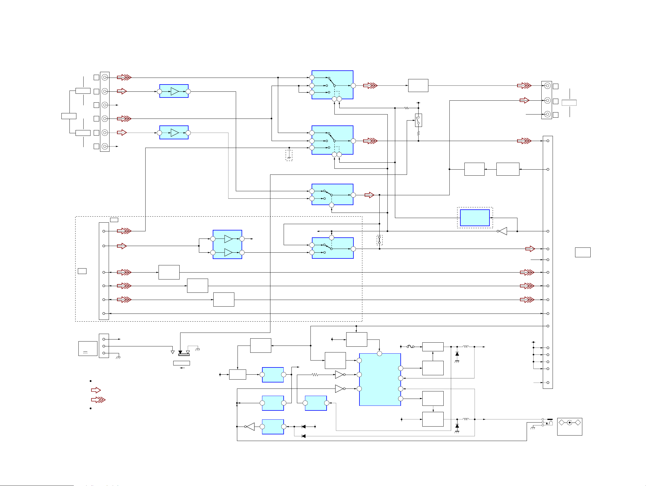
6-1. BLOCK DIAGRAM — CONNECTION BOX SECTION —
XA-126: AEP, UK model, XA-125: US, Canadian, E, Chinese model
XVM-F65WL
Ver. 1.1
JK1101
INPUT
JK1101
V
VIDEO 2
VIDEO 1
AEP,UK MODEL
J1501
RGB
POWER
DC IN 12V
3A
SYNC
AU-IN
EXT-R
EXT-G
EXT-B
NC
L
R
V
L
R
J1501
2
8
1
6
4
3
CN1851
4
2
1
Signal path
: AUDIO
: VIDEO
R-ch is omitted due to
same as L-ch
RGB
R-CH
R-CH
BATT
IC1201 AUDIO AMP
5 7
IC1101 AUDIO AMP
5 7
VIDEO RED
SIGNAL AMP
Q1501
S1431
LOCATION
FRONT REAR
VIDEO GREEN
SIGNAL AMP
Q1511
IC1541 AUDIO AMP
3
5
VIDEO BLUE
SIGNAL AMP
Q1521
BATT
+5V REG
Q1871
1
7
Q1951
R-CH
POWER
CONTROL
Q1872,1873
5 4
1 2
1 2
+3.3V REG
IC1871
VOLTAGE
DET
IC1941
VOLTAGE
DET
IC1951
US,CND,E
MODEL
IC1401 VIDEO SELECT
VIN2
3
VIN1
1
VIN3
5
IC1402 VIDEO SELECT
VIN2
3
VIN1
1 7
VIN3
5
IC1131 AUDIO SELECT
IN2
3
IN1
1
R-CH
IN1
1
IN3
3
IC1543 AUDIO SELECT
BATT
CONVERTER
+3.3V
VOLTAGE
DET
1 2
IC1841
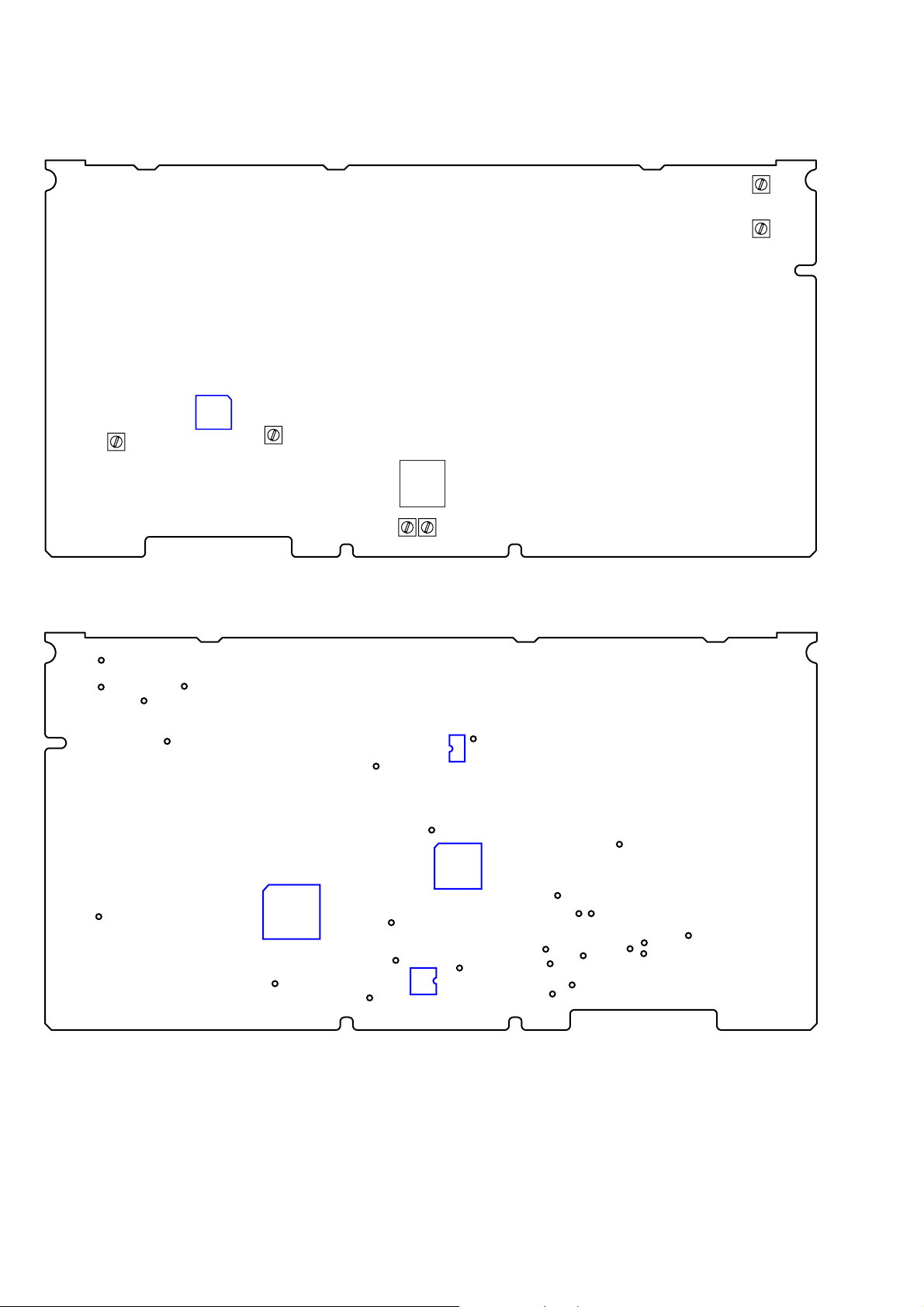
8V
2 4
2 4
2
2
DC-DC
CONTROL
Q1822
VOUT
VOUT
OUT
OUT
Q1821
Q1921
7
7
7
POWER
CONTROL
Q1824,1825
15
11
6
SCP
DT2
DT1
9
VCC
DC-DC
CONVERTER
IC1801
US,CND,E,CH
MODEL
BATT
OUT2
NON2
NON1
OUT1
BATT
10
14
3
7
VIDEO AMP
F1801
Q1401
8V
Q1433,1434
LOCATION
SW CONTROL
Q1803
SWITCHING
SWITCHING
DRIVE
Q1801,1802
SWITCHING
DRIVE
Q1901,1902
SWITCHING
DRIVE
Q1903
MUTE
Q1301
AEP,UK MODEL
VIDEO SW
CONTROL
IC1421,Q1422,1423
D1801
D1901
+8V
MUTE DRIVE
Q1351-1353
Q1421
R-CH
R-CH
BATT
JK1401
V
JK1401
L
OUTPUT
R
CN1861
10
CVBS/SYNC
12
A-MUTE
14
V-SW
J1901
–
DC OUT 9V
MAX 1A
CN1861
MONITOR
(XVM)
+
5
AUDIO-L-CH
1
AUDIO-R-CH
7
EXT-R
8
EXT-G
3
EXT-B
15
NC
11
PW-ON
8V
13
8V
17
8V
18
8V
19
8V
16
+B-DET
XVM-F65WL
17 17
Page 18

XVM-F65WL
6-2. BLOCK DIAGRAM — VIDEO SECTION —
CN904
16
EXT-R
15
EXT-G
14
EXT-B
IC102
VIDEO SW
13
TO
CONNECTION
BOX
CN1861
CVBS/SYNC
1
2
3-6
22
POWER ON
24
SIRCS
21
A MUTE
23
V-SW
20
AU-L
18
AU-R
BATT
LITIUM
8V
D105
POWER
(Page 19)
4
PARKING DET
Q406,407
VIDEO
AUDIO-L
AUDIO-R
Q409
CONTROL
RECEIVER
V-SW
BUFFER
1
3
REMOTE
1
IC404
VD PULSE
SHAPE
Q505
34 35
R
8
G
9
B
2
1
L
R
OUTL
OUTR
10
CSYNCIN
46
C IN
57
Y IN
52
IC401 (1/2)
SYSTEM CONTOL
32
PW_DETLITIUM
48
2.4G-ON1
64
PARKING
PW_ON
2
44
HALT
47
REM_IN
S-SDA
7
S-SCL
6
AMUTE
53
63
SW1
SW2
62
+5V REG
1 8
IC201
SYNC
SEP
BPF/
ACC
SW
53
SYNC_DET
V-SDA
V-SCK
DATA
CLK
OSD
IR ON
P57
AMP ON
CS
VD
3
SYNC
SEP
Q501,502
7
2
BATT
Q405
10
9
6
5
8V 6V
+3.3V
1 3
REG
IC103
Q408
14 13
SW
SELECT
/VOL
IC301
AUDIO SELECT,
ELECTRONIC VOLUME
2 1
INITIAL
MUTE
IC252
3.3V
16
17
CSYNCOUT
HH
KILL
Q355
L
IN
16
R
IN
1
IC251
SPEAKER AMP
1
6
G-Y
GEN
DELAY/
SHARP
HSYNC LOCK
H PULSE
SHAPE
Q506,507
AUDIO IR
TRANSMITTER
AGC
AGC
5
8
MATRIX SW
SDATA
SCLK
48 14161517161817
IC351
PRE
EMPHASIS
PRE
EMPHASIS
R-Y/B-Y
DEMOD
SYNC
OUT
TRAP
21
17
16
19 3
20 1
22 2
43
49
8
5
VD IN
DATA
SCLK
CSN
VREF
FO SW
LEVEL
DETECT
VREF
SP251
SPEAKER
VCO I/N
OSD
SW
R_IN2
G_IN2
VRVGVB
OUTPUT
CONTROL
B_IN2
YS
VBLK
15
VIDEO RAM
610
VCO
VC0
11
V
COUNT
BRIGHT/
CONTRAST
VXO
CG
ROM
L-CH
VCO
R-CH
VCO
OUT
OUT
63 64473954
IC551
L
9
R
8
X501
3.585MHz
CHARACTER GENERATER
RV352
BUF
BUF
RV351
DATA
INVERT
SELECT
IC501
RGB DECODER
X502
4.43MHz
H
COUNT
V
COUNT
AUDIO IR
AMP
Q352,356,358
AUDIO IR
AMP
Q351,357,359
RGB
OUT
VCOMOUT
HD OUT
32
VD OUT
31
BLAK
18
R
26
G
21
B
19
POL
36
28
TRAP
CONTROL
Q503,504
H SYNC
OSC
V SYNC
D354 D352
Signal path
: AUDIO
: VIDEO
PCL
20
19
4
DRIVE
Q353,354
HD
(Page 19)
2
VD
BLK
R
G
B
POL
VCOM
PAL
HDOUT
Q551
REG
IR
8V
1
3
VDD3.3V
(Page 19)
(Page 19)
XVM-F65WL
1818
Page 19

6-3. BLOCK DIAGRAM — DISPLAY SECTION —
IC701
SWITCHING
REGULATOR
2
FREQUENCY
COMP
RV702
DC-DC
PWM
ERROR
OSC
Signal path
: VIDEO
BATT
AMP
(Page 18)
(Page 18)
(Page 18)
POWER
DET
Q402
PWM
COUT
SCP
LCD-VCC
DET
Q410
7
3
15
B+ SWITCH
ON/OFF
DRIVE
Q701,702
Q101,102
T701
8V
RF UNIT
8V
RF101
2
3
LED1+5V6V
LED2
LED3
LED4
Q403
D701
D702
D703
D704
D705
1
HD OUT
53
6
8
9
BLK
PAL
POL
VCOM
R
G
B
HD
VD
VGON 17V
9V
VDD3.3V
VSS-13V
EEPROM
IC403
LED
DRIVER
Q106-109
RV701
SW REG
X401
4.19MHz
5
6
VEE5V
23
N/P
45
PW IN
13
SDA
14
SCL
SYSTEM CONTROL
31
P12/ANI2
55
2.4G-ON2
40
X2
41
X1
50
CH1
CH2
51
52
CH3
CH4
54
IC401 (2/2)
SIED 1
SIDE 2
ZOOM
JUST
KEY1
KEY2
RESET
TFT_ON
DIMMER
59
58
57
61
30
29
36
56
60
RV651
NC
KEY MATRIX
S402-407
RESET
1 2
IC402
S401
(RESET)
IC651
VCO
3
4
H
COUNT
V
COUNT
FIELD DET
INT/EXT
SEL
5
7
DISPLAY CONTROL
3336
PDVCOI
PLL
DET
COM
OSC
IC652
8 13
PULSE
STEERING
F/F
BACK LIGHT CONTROL
OUT
OUT
16
PWM
COMP
IC601
H
V
RV652
VCOM
BIAS
IC801
ERROR
AMP
ERROR
Q652,654,655
AMP
1
VT
D601
OSC
HD OUT
6
HSYNC IN
2
VDBIN
5 16
NBLK
8 20
NP1
46 19
POL
14 17
VD OUT
7
4
QHSEL(SIDE1)
CPHSEL(SIDE2)
3
12
LTBOX(ZOOM)
3.3V
MASK
V
SEL
JUST
31
8V
29
27
25
23
24
26
18
21
VCOM
DRIVE
XVM-F65WL
RED
GREEN
BLUE
CPH1
CPH2
CPH3
STH1
STH2
CPV
STV1
STV2
OEV1
OEV2
OEV3
OEH
VCOM
T801
2
1
BACK LIGHT
DIMMER
CONTROL
Q802
LCD1
LCD
XVM-F65WL
VIDEO
AUDIO-L
AUDIO-R
10
1
2
BUFFER
Q104
BUFFER
Q105
VIDEO
AUDIO-L
AUDIO-R
4
(Page 18)
19 19
Page 20

XVM-F65WL
Ver. 1.1
• NOTE FOR PRINTED WIRING BOARDS AND SCHEMATIC DIAGRAMS
THIS NOTE IS COMMON FOR PRINTED WIRING
BOARDS AND SCHEMATIC DIAGRAMS.
(In addition to this, the necessary note is
printed in each block.)
for schematic diagram:
• All capacitors are in µF unless otherwise noted. (p: pF)
50 WV or less are not indicated except for electrolytics
and tantalums.
• All resistors are in Ω and 1/
specified.
•%: indicates tolerance.
f
•
• C : panel designation.
Note: The components identified by mark 0 or dotted line
• A : B+ Line.
• B : B– Line.
• H : adjustment for repair.
• CN901 of XVM-F65WL is connected to Connection Box
•Voltages are taken with a VOM (Input impedance 10 MΩ).
•Waveforms are taken with a oscilloscope.
• Circled numbers refer to waveforms.
• Signal path.
•Abbreviation
: internal component.
with mark 0 are critical for safety.
Replace only with part number specified.
with a monitor cable.
Power voltage is dc 14.4 V from BATT cord of the Connection Box and fed with regulated dc power supply.
Voltage and waveforms are measured at input the color
bar signal from the Connection Box.
Voltage variations may be noted due to normal production tolerances.
Voltage variations may be noted due to normal production tolerances.
F : AUDIO
g : VIDEO
CND : Canadian model.
CH : Chinese model.
4
W or less unless otherwise
for printed wiring boards:
• X : parts extracted from the component side.
• Y : parts extracted from the conductor side.
• : Pattern from the side which enables seeing.
Caution:
Pattern face side: Parts on the pattern face side seen from the
(Side B) pattern face are indicated.
Par ts face side: Parts on the parts face side seen from the
(Side A) parts face are indicated.
C
Q
B
E
Q
BCE
Q
B
C
•Abbreviation
CND : Canadian model.
CH : Chinese model.
These are omitted.
These are omitted.
E
XVM-F65WL
2020
Page 21

• Waveforms (MONITOR Board)
XVM-F65WL
1 IC501 eh (POL)
µ
sec
127
1 V/div, 50 µsec/div
2 IC501 rh (CSYNCIN)
H
0.5 V/div, 20 µsec/div
3 IC501 ts (YIN)
6 IC501 ql (B-OUT)
3.1 Vp-p 3.4 Vp-p
2H
1 V/div, 20 µsec/div
7 IC501 wa (G-OUT)
0.8 Vp-p
2H
1 V/div, 20 µsec/div
3.4 Vp-p
8 IC501 wh (R-OUT)
1 Vp-p
3.4 Vp-p
qa IC801 8 (OUTL)
µ
sec
20
2 V/div, 5 µsec/div
qs IC401 r; (X2)
4.19 MHz
1 V/div, 100 nsec/div
qd IC601 eh (VCO1)
8.0 Vp-p
3.6 Vp-p
3.0 Vp-p
qh IC601 6 (HOUT)
H
1 V/div, 20 µsec/div
qj IC652 1 (OUT1)
127
µ
sec
2 V/div, 20 µsec/div
qk CN701 1 (VCOM)
3.2 Vp-p
6.0 Vp-p
6.0 Vp-p
wa CN701 6 (BLUE)
2H
1 V/div, 20 µsec/div
ws Q702 C (TP703)
4.2
µ
sec
10 V/div, 2 µsec/div
wd IC102 1 (VIN1)
3.4 Vp-p
22 Vp-p
1.0 Vp-p
H
0.5 V/div, 20 µsec/div
4 IC501 tj (CIN)
H
0.5 V/div, 20 µsec/div
5 IC501 ys (SCOUT)
3.5795 MHz
0.2 V/div, 200 nsec/div
1 Vp-p
0.7 Vp-p
2H
1 V/div, 20 µsec/div
9 IC501 ea (VDOUT)
V
1 V/div, 2 msec/div
0 IC501 es (HDOUT)
H
1 V/div, 20 msec/div
3.2 Vp-p
3.2 Vp-p
41.7 nsec
0.5 V/div, 200 nsec/div
qf IC601 2 (HSYNCIN)
H
1 V/div, 20 µsec/div
qg IC601 5 (VDBIN)
V
1 V/div, 2 msec/div
3.2 Vp-p
3.2 Vp-p
127
µ
sec
2 V/div, 20 µsec/div
ql CN701 4 (RED)
2H
1 V/div, 20 µsec/div
w; CN701 5 (GREEN)
2H
1 V/div, 20 µsec/div
3.4 Vp-p
3.4 Vp-p
H
0.5 V/div, 20 µsec/div
wf IC102 7 (VO)
1.0 Vp-p
H
0.5 V/div, 20 µsec/div
XVM-F65WL
21 21
Page 22

XVM-F65WL
Ver. 1.1
6-4. PRINTED WIRING BOARD — CONNECTION BOX SECTION —
XA-126: AEP, UK model, XA-125: US, Canadian, E, Chinese model
: Uses unleaded solder .
CON-BOX BOARD (SIDE A)
D1421
D1104
D1106
US,CND,E,CH MODEL
US,CND,E,CH MODEL
C1556
D1103
D1105
C1555
5
8
5
8
IC1543
IC1544
D1861
AEP,UK MODEL
4
1
R1541
4
1
R1542
C1551
C1552
L1803
TH1861
Q1825
ECB
C1831
R1832
R1831
ECB
Q1822
R1808R1806
234567891011121314
1
A
B
F1901
L1902L1903
L1901
C
R1835
R1836
Q1824
BCE
D
L1802
L1801
IC1421
• Semiconductor Location
Ref. No. Location
D1101 F-7
D1103 C-12
D1104 C-12
D1105 B-11
D1106 C-12
D1201 F-8
D1421 B-13
D1861 B-11
IC1131 F-6
IC1132 F-4
IC1421 F-12
Ref. No. Location
IC1543 C-11
IC1544 D-11
Q1301 F-5
Q1302 F-5
Q1421 F-12
Q1422 F-12
Q1423 F-12
Q1822 D-8
Q1824 D-4
Q1825 D-9
Q1421
R1424
R1422
54
81
AEP,UK MODEL
ECB
R1421
R1423
ECB
R1425R1426
Q1422
R1437
BCE
R1427
Q1423
C1421
R1413
L1402
L1401
R1404
R1402
R1403
R1401
R1201
C1201
R1202
C1213
L1201
C1203
R1229
C1202
D1201
C1204
R1101
C1101
R1102
R1129
C1103
C1102
C1104
D1101
C1105
C1205
C1113
L1131
L1101
1
IC1131 IC1132
4
R1130
8
5
Q1301
BCE BCE
R1303
Q1302
R1304
C1106
C1206
F1801
1
4
8
5
R1131
E
F
G
1-866-334-
21
H
XVM-F65WL
2222
Page 23

XVM-F65WL
Ver. 1.1
A
B
C
D
E
F
G
H
1
234567891011121314
CON-BOX BOARD (SIDE B)
VDR851
D1851
L1851
R1435
D1352
D1351
R1357
R1355
ECB
C1351
Q1353
S1431
S1431
LOATION
FRONT REAR
Q1352
C1352
BCE
R1354
R1352
BCE
Q1351
R1353
R1356
BP1851
R1351
FB1801
C1353
TP1853
C1853
C1894
DC IN 12V
C1852
C1801
CN1851
POWER
TP1852
CN1851
C1851
C1893
3A
TP1851
Q1802
C1802
FB1802
D1801
43
21
ECB
R1302
C1302
R1942
C1901
C1902
D1901
FB1902
R1903
C1905
R1801
R1803
ECB
Q1801
1
4
Q1803
85
R1842
TH1841
C1304
R1306
C1306
TP1152
TP1154
RL
R1802
FB1901
Q1902
BCE
R1902
C1805
R1804
R1308
TH1941
85
Q1903
14
Q1901
BCE
R1904
C1904
R1901
C1827
C1804
C1824
R1823
5
4
IC1841
13
C1303
R1305
TP1151
C1132
R1301
C1908
R1928
R1941
R1906
R1925
C1924
R1923
C1828
Q1821
R1825
BCE
C1826
C1841
R1843
R1828R1841
C1131
TP1112
R1307
C1301
TP1153
JK1401 JK1101
C1907
IC1941
45
312
R1943
R1908
R1907
C1923
R1922
18
IC1801
169
C1823
C1825
R1824
C1114 C1112 C1214
TP1111
C1305
D1411
D1412
R1935
R1931
BP1821
R1822
C1111
C1926
C1925
C1921
TP1451
R1934
TP1902
R1927
R1924
R1821
IC1101
V
TP1901
R1933
R1909
D1923
ECB
Q1921
D1921
R1921
C1821
R1827
58
41
TP1212
TP1452
VIDEO 1 VIDEO 2
TP1903
D1951
R1952
ECB
D1922
Q1951
R1951
C1211
TP1103
R1104
D1952
D1821
D1823
TP1104
J1901
–
DC OUT 9V
MAX 1A
R1953
IC1951
C1808
TP1211TP1113
IC1201
TP1204
R
+
C1911
R1955
R1956R1957
123
54
58
41
D1822
C1807
C1212
TP1203
R1204
Q1873
ECB
BCE
C1912
Q1872
R1871
D1871
C1872
C1871
IC1871
3
R1954
R1406
45
C1873
R1809
Q1401
BCE
R1405
C1406
C1401 C1402 C1415 C1407
TP1101
R1103
TP1102
VIDEO 1 VIDEO 2
Q1871
B C E
TP1861
1
TP1164
TP1202
L
INPUTOUTPUT
R1872
C1404
C1405
R1873
IC1401
C1812
R1433
AEP,UK MODEL
58
US,CND,E,
41
CH MODEL
AEP,UK MODEL
TP1201
R1203
TP1403
TP1863
C1811
C1545
R1541
Q1434
ECB
C1554
Q1433
ECB
R1434
TP1419
TP1418
C1410
R1410
R1415
C1412
C1403
TP1415
TP1401
D1401 D1403
D1402 D1404
VIDEO 1 VIDEO 2
V
TP1162
C1544
C1546
C1553
IC1541
US,CND,E,CH
MODEL
R1409
C1411
IC1402
TP1402
MONITOR
TP1864 TP1865
16 21
11 15
5
1
TP1161
C1542
58
41
C1541
C1414
58
41
C1408
TP1416
TP1509
TP1501
TP1163
R1545
D1543
C1547
R1543
R1544
TP1503
C1409
D1503
TP1417
D1505
TP1507
D1507
64 78
31 25
D1504
TP1505
TP1508
CN1861
(XVM)
CN1861
4
TP1462
AEP,UK MODEL
L1501
C1543
R1503
R1513
D1506
R1523
D1508
TP1502
D1509
J1501
J1501
RGB
10
TP1461
D1413
D1414
C1506
R1504
R1514
R1524
D1502
TP1504
TP1862
TP1463
C1505
C1501
C1511
C1521
D1501
TP1561
Q1501
BCE
R1505
R1506R1515
Q1511
BCE
R1516
BCE
R1525
Q1521
R1526
TP1563
TP1564TP1562
R1507
R1517
R1527
1-866-334-
C1512 C1502
C1522
21
XVM-F65WL
• Semiconductor Location
Ref. No. Location
D1351 F-3
D1352 F-2
D1401 G-10
D1402 G-10
D1403 G-11
D1404 G-11
D1411 G-7
D1412 G-7
D1413 C-13
D1414 C-13
D1501 G-13
Ref. No. Location
D1502 G-13
D1503 E-12
D1504 E-12
D1505 F-12
D1506 F-12
D1507 F-12
D1508 F-12
D1509 G-12
D1543 D-12
D1801 E-4
D1821 C-8
23 23
Ref. No. Location Ref. No. Location
D1822 C-9
D1823 D-8
D1851 C-2
D1871 B-9
D1901 B-5
D1921 C-8
D1922 C-8
D1923 C-7
D1951 B-8
D1952 B-8
IC1101 F-7
IC1201 F-8
IC1401 F-10
IC1402 F-11
IC1541 D-11
IC1801 D-6
IC1841 E-5
IC1871 C-9
IC1941 B-7
IC1951 C-8
Ref. No. Location Ref. No. Location
Q1351 F-2
Q1352 F-2
Q1353 G-3
Q1401 E-9
Q1433 D-11
Q1434 D-11
Q1501 E-13
Q1511 E-13
Q1521 F-13
Q1801 D-5
Q1803 E-5
Q1821 D-6
Q1871 B-9
Q1872 B-9
Q1873 B-9
Q1901 C-5
Q1902 C-5
Q1903 B-6
Q1921 C-7
Q1951 C-8
Q1802 D-4
Page 24

XVM-F65WL
Ver. 1.1
6-5. SCHEMATIC DIAGRAM — CONNECTION BOX SECTION (1/2) —
XA-126: AEP, UK model, XA-125: US, Canadian, E, Chinese model
• Refer to page 33 f or IC Block Dia grams.
J1501
D1403
D1404
JK1101(1/2)
TP1402
TP1201
TP1202
TP1203
TP1204
JK1101(2/2)
TP1401
TP1403
TP1101
TP1102
TP1103
TP1104
TP1503
TP1501
TP1509
TP1507
TP1502
TP1505
TP1508
TP1504
R1203
R1204
R1103
R1104
D1401
D1402
R1201
R1202
R1101
R1102
C1101
C1102
D1503
D1504
D1502
D1501
D1507
D1508
D1506
D1505
D1509
C1201
C1202
R1543
L1201
IC B/D
L1101
IC B/D
C1213
IC1201
C1113
IC1101
C1546
IC B/D
IC1541
C1203
C1204
C1103
C1104
C1542
C1541
C1214 C1212
C1211
D1201
C1114 C1112
C1111
D1101
C1545 C1544
TP1211
TP1212
R1229
TP1111
TP1112
R1129
L1541
TP1113
C1105
C1205
C1106
C1206
L1131
C1131
R1401
TP1415
TP1416
IC B/D
TP1417
TP1419
IC1131
IC1132
C1132
R1402
C1401
C1402
C1407
C1408
R1403
IC B/D
IC1401
R1404 C1415
R1437
IC1402
C1409 C1411
R1409
IC B/D
C1414
R1415
C1410
L1402
C1403
R1413
C1404
C1412
TP1418
R1410
R1434
R1130
R1131
C1405
Q1433
C1301
Q1301
R1303
R1304
Q1302
C1302
R1405 C1406
Q1401
R1436
Q1431
Q1434
R1301
R1305
R1306
R1302
R1406
Q1432
R1431
R1307
C1303
C1304
R1308
L1401
R1433
R1432
R1421
C1421
R1422
Q1421
C1305
C1306
D1411
D1412
R1424
R1425
R1426
C1894C1893
TP1451
TP1452
TP1151
TP1153
TP1152
TP1154
R1423
IC1421
R1427
Q1423
Q1422
JK1401
XVM-F65WL
R1544
C1501
R1503
R1506 R1507
R1504
C1511
R1513
R1516 R1517
R1514
C1521
R1523
R1526
R1524
R1505
R1515
R1525
C1547
Q1501
Q1511
Q1521
C1543
R1527
D1543
C1505
C1522
C1506
C1502
C1512
R1545
C1552
C1554
IC B/D
C1551
C1553
IC1544
IC1543
IC B/D
2424
R1541 R1542
(Page 25)
C1556L1501
C1555
D1413
D1104
D1106
D1414
D1861
D1421
D1103
D1105
TP1161
TP1163
TP1563
TP1462
TP1162
TP1564
TP1561
TP1562
TP1461
TP1861
TP1164
TP1463
TP1862
TP1863
TP1864
TP1865
CN1861
Page 25

6-6. SCHEMATIC DIAGRAM — CONNECTION BOX SECTION (2/2) —
XA-126: AEP, UK model, XA-125: US, Canadian, E, Chinese model
XVM-F65WL
Ver. 1.1
• Refer to page 33 f or IC Block Dia grams.
(Page 24)
C1812
L1803
R1809
R1806
C1808C1811
R1808
IC B/D
L1802
D1801
C1807
FB1801
IC1871
R1841
TH1841
R1842
C1841
R1843
Q1803
C1871
Q1871
D1871
R1871
C1872
IC1841
R1804
Q1802
Q1801
R1872
R1873
Q1872
Q1873
C1804
R1802
C1805
FB1802
R1803
R1801
F1801
C1802
C1353
L1801
Q1353
D1352
C1801
C1352
R1357
R1355
R1356
C1821
C1351
Q1352C1873
D1351
R1821
R1822
C1925
R1924
R1922
R1354
C1921
R1353
R1921
Q1822
R1823
C1823
R1923
Q1351
C1924
R1351
R1352
R1831
C1824
R1925
R1832
C1831
R1825
R1824 C1825
C1923
C1828
C1827
IC B/D
IC1801
C1851
R1836
Q1921
Q1824
TH1861
C1852
Q1825
C1826
R1927
R1835
Q1821
R1827
C1926
D1851C1853
VDR851
D1823
D1923
R1828
S1431
L1851
D1821
D1822
R1435
TP1851
BP1851
TP1853
TP1852
CN1851
XVM-F65WL
J1901
TP1901
TP1902
TP1903
D1951
D1952
R1955
R1956
R1957
L1903 L1902
C1912
C1911
R1906
R1907
R1909
R1908
C1908
D1901
C1907
FB1901
IC1951
Q1903
TH1941
R1942
R1943
R1941
IC1941
FB1902
Q1901
R1904
Q1902
R1901
C1904
R1902
C1905
R1903
25 25
F1901
C1902
R1934
R1933
R1928
C1901
R1954
R1935
R1931
R1953
R1952
R1951
D1921
D1922
Q1951
Page 26

XVM-F65WL
6-7. PRINTED WIRING BOARDS — MONITOR SECTION —
MONITOR BOARD (SIDE A)
IC404
13
C412
D406
L402
RB602 RB601
R622
R638
R670
Q654
FB603
FB604
FB605
R664
FB609
R669
R661R662
RV652
R672
R666
C657
L653
C659
R663R665
5
IC652
8
Q655
R673
ECB ECB
Q652
C658
C660
R674
4
1
R671
L654
C661
• Semiconductor Location (MONITOR Board)
Ref. No. Location
D201 B-6
D352 D-1
D354 D-1
D402 F-6
D404 E-5
D405 E-6
D406 D-14
D601 F-10
D602 F-10
D701 F-8
D702 G-8
Ref. No. Location
D703 G-8
D704 G-8
D705 H-8
D801 G-2
IC103 D-4
IC201 B-6
IC301 B-8
IC351 B-3
IC403 G-5
IC404 C-14
Ref. No. Location Ref. No. Location
IC551 G-5
IC601 E-11
IC652 F-13
IC801 G-2
Q351 B-2
Q352 B-2
Q402 E-6
Q403 F-6
Q409 D-5
Q410 E-6
R619
R621
13
RB603RB604
24
R634
FB610
FB611
C610
CN701
LCD1
LIQUID CRYSTAL
DISPLAY PANEL
12
IC601
25 36
C611
C612
1
L602
C608
C613
48
C606
37
C605
R603
R602
C729
130
: Uses unleaded solder.
R608
R607
R604
L604
R722
D601
R653
L652
L712C728
D602
L603
C607
L601
C601
RV651
C651
L651
L711
L710
L708
L709
FB602
R605
C603
C604
R723
C727
C726
C724
C725
Q501 D-8
Q502 E-8
Q505 F-9
Q512 F-9
Q513 F-9
Q652 G-13
Q654 F-13
Q655 F-13
Q702 G-7
Q802 G-2
R652
R651
L504
C312
C322
C302
C301
C323
C546
C723
R566
C720
C730
C722
R563 R534
ECB ECB
Q505Q512
R565
R564
C719
L705
L706
L707
L704
C714
L703
R306
C324
R526
C538
Q513
ECB
R305
C566
R533
R302
R505
C567
C545
R532
C715
C716
C717
C718
R567
R301
R501
R525
A K
C313
C314
C317
C318
R304C304
D701
D702
D703
D705
L503
A K A K A K A K
R303
C303
C501
C503
C504
VR301
VR302
Q501
D704
R307
R308
R504
R502
Q502
C536
1
12
ECBECB
RV701
C535
C534
C502
IC301
C320
L501
R503
C564
C533
T701
BATT PLUG BOARD (SIDE A)
R904
C307
C321
C531
C532
RV702
R711R702R701
F902
C306
C308
24
R311
C309
C310
R312
C311
13
L301
X501
X502
C528
C529
C530
1-866-332-
C
R315
R314
R316
R313
C710
R309
R310
C712
R719
C525
C526
C527
Q702
21
18
L702
R516
R517
R518
C713
L201
C201
C515 C514
E
B
C203
IC201
45
C202
24 1
CN904
R405
D405
C418
F701
EBC
EBC
Q403
R433
R434
C409
Q402
BCE
R422
R423
R551
R404
Q410
D402
R401
R552
R432
D201
C562
C411
R430
R431
C410
C408
C404
11
20 1
C561
L551
L202
C210
R415
R403
R491
IC551
D404
C407
R490
C552
MONITOR SUB BOARD (SIDE A)
R901
C902
GSD
C901
R902
Q903
BCE
Q902
D903
D901
R903
C903
9
81
R454
C421
R455
C416
R429
R468
X401
R469
R473
R476
R477
R479
C414
R480
18
IC403
45
C554
C553
C555
10
L552
R558
16
CN901
ECB
Q409
L252 L253
C258
C257
CN252
12
WHT
C114
C113
1
IC103
3
C112
L401
C402
CN903
24 1
BLK
C401
L801
F901
F903
1-866-333-
R259
2
F801
D902
SP251
SPEAKER
C351
R353
R351
R352
R354
C352
R819
R818
21
C353
C806
C805
C804
C803
C356
16
1
IC351
C816
R815
R804
R802
R360
9
8
C355
C821
C808
112010
C807
C810
234567891011121314
RV351
C358
B
Q352
R366
R367
C815
IC801
C
E
B
C
Q351
E
RV352
CN801
1
2
T801
C818
R816
C814
R814
C813
C812
C811
1
R806
R812
BCE
R809
R811
R810
R805
R820
Q802
R808
• Semiconductor
Location
(MONITOR SUB
Board)
Ref. No. Location
D901 I-6
D902 I-4
D903 I-6
Q902 I-6
Q903 I-6
R378
R379
R813
D801
JC354
1-866-331-
WHT
PNK
D354
D352
1
A
B
LCD
C
BACK
LIGHT
D
E
F
G
21
H
I
XVM-F65WL
2626
Page 27

XVM-F65WL
A
B
C
D
E
F
G
H
I
XVM-F65WL
1
234567891011 12 13 14
MONITOR BOARD (SIDE B)
Q358
C362R370C363
D409
C361
R371
C364
TP808
R374R380
Q359
R375
R381
R817
C817
BCE
BCE
F351
TP356
S407
INPUT
JC353
TP408
S405
DIMMER
JC351
TP409
S406
MENU
R443
TP354
R496
TP804
TP405
TP352
R368
R369
R372
ECB
Q356
R373
ECB
Q357
TP807
R376
R377
BCE
TP802
TP801
C359
Q355
C4
C819
Q354
TP805
C357
C354
BCE
R364
TP809
R365
Q353
TP353
BCE
TP351
TP355
L351
C801
C360
TP252
IC251
R260
TP806
C255
R256
TP251
R261
C254
R255
41
58
C256
IC252
135
4
TP934
TP407
S401
(RESET)
R406
R257
C403
R407
R258
D202
TP935
TP410
TP406
C413
R474
R475
R478
R253 C253
C259
R254
C260
R464
D408
R460
R466
RB401
RB402 RB403
R424
R408
R409
R410
Q407
ECB ECB
Q406
R463
R465
C420
C419
RB408
64
1
16
17 32
TP555
R555
R553
C560
C559
MONITOR SUB BOARD (SIDE B)
TP901
TP902
TP916
TP906
TP904
TP915
TP917
TP940
TP952
TP913
TP912
TP907
TP906
TP201
R462
R554
R251
TP932
RB407
R561
C565
BCE
C558
TP909
C108
TP933
R461
IC401
R557
TP910
C415
Q551
R556
R562
C556
D912
D913
RB406 RB405
R451
R489
R492
TP908
TP911
R203
C209 R206 R202
D107
R118
TP922
49
48
33
R493
R494
R440
R495
TP903
R444
R436
Q405
BCE
R439
D106
R414
C406
R413
C405
R412
R411
R204
R205
R453
RB404
C208
TP925 TP924
TP930
TP921
R452
ECB
13
IC402
54
TP919
R437
R438
R435
TP914
TP926
TP920
TP928
D505
D504
Q408
TP554
1-866-333-
TP502
TP929
C206
C207
TP923
L701
R543
TP927
D506
TP552
TP704
R718
TP702
13
64
Q701
TP703
21
C315
C316
C319
TP501
C105
C110
R101
C513
C512
R507
TP505
64
1
16
17 32
C732
R709
R710
C705
TP701
C704
16
R708
R704
R703
C701
C511
R522
R705
85
IC102
14
C509
C510
IC501
R523
TP710
C508
R524
TP509
C107
C507
R506
49
C537
R103
L505
C506
48
33
R532
C118
R716
R717
R715
C709
R714
L101
R102
D108
TP503
C520
C521
C522
TP506
C524
TP553
R512
R513
R514 R515
TP551
C706
R712
C707
R713
C708
81
IC701
9
C733
C702
R707
R706
C703
BATT PLUG BOARD (SIDE B)
CN902
27 27
Q102
123
BCE
C505
R535
C109
R104
R106
C121
C517
R527
R528
C539
R529
C544
R539
R540
C548
1-866-332-
Q101
Q503
C540
R531
BCE
BCE
R509
R536
R537
C542
R530
R538
BCE
Q507
C101
C541
R508
C653
C663
TP508
R655
C654
TP108
R656
R657
R659
TP712
C609
FB601
C615
C602
C614
TP714
RF101
(RF UNIT)
TP109
Q106
R658
C655
R660
TP110
R636
TP713
TP715
TP723
R637
TP507
C618
TP718
R635
R620
C617
TP720
TP719
TP711
TP717
R721
C616
TP716
D706
TP725
R633
TP722
D707
TP653
TP726
FB608
TP724
FB607
C117
L102
R113
R116
Q104 Q105
BCE
BCE
R111 R114
TP105
C116
TP103
TP510
TP709
R105
TP104
TP652
C115
TP101
TP102
110
Q504
BCE
C519
C543
D501
C518
Q506
ECB
L502
R541
TP511
TP504
TP705
TP707
TP708
TP107
TP106
BCE BCE ECB ECB
Q109 Q108 Q107
R610
C652
R654
54
13
IC651
TP651
R601
C656
TP706
TP734
TP732
TP730
• Semiconductor Location
Ref. No. Location
D105 B-14
21
D106 C-6
D107 C-6
D108 C-7
D202 B-4
D407 H-13
D408 D-5
D409 H-2
D501 E-9
D504 E-6
D505 D-6
D506 E-7
D706 G-12
Ref. No. Location
D707 G-12
D912 D-6
D913 D-6
IC102 C-8
IC251 B-4
IC252 C-4
IC401 F-5
IC402 G-6
IC501 E-8
IC651 F-11
IC701 G-7
S402
POWER
D105
POWER
R117
TP401
TP729
TP654
TP727
FB606
TP731
TP721
TP726
TP402
D407
TP404
R441
TP403
S403
VOLUME
R442
S404
1-866-331-
Ref. No. Location Ref. No. Location
Q101 C-9
Q102 C-9
Q104 C-9
Q105 C-10
Q106 D-11
Q107 D-11
Q108 D-10
Q109 D-10
Q353 B-3
Q354 B-3
Q355 B-3
Q356 B-2
Q358 A-2
Q359 B-3
Q405 G-6
Q406 D-5
Q407 D-5
Q408 E-6
Q503 D-9
Q504 D-9
Q506 E-9
Q507 F-9
Q551 G-5
Q701 G-7
Q357 B-2
21
Page 28

XVM-F65WL
6-8. SCHEMATIC DIAGRAM — MONITOR SECTION (1/4) —
Q501
R502
R508
R509
C501
L501
Q504
C502
R501
C517
Q503
TP504
C503
R503
L505
C516
C513
C514
C515
TP501
TP502
• Refer to page 21 for Waveforms. • Refer to page 32 for IC Block Diagram.
TP511
Q507
C545
R532
TP510
TP508
TP507
L503
R541
C536
R524
C535
C534
C533
R523
C532
R522
C546
C537
C531
R504
C506
C511
R507
C512
C505
R506
C507
C508
C509
C510
X501
L502
R505
X502
C518
TP503
IC B/D
Q502
C504
C519
C564
C567
R525
TP509
C520
R536 R538
R537
C539
R528
C540
R527
R526
TP505
C538
TP506
C521
C522
R529
C542
R530
C524
C541
IC501
C525
C543
C526
C527
R531
C528
D501
C529
C544
C530
R539
Q506
R540
C548
R535
L504
R533
R564
Q505
R534
C566 R563
R565
R566
Q513
Q512
R567
(Page 31)
(Page 29)
TP807
TP806
R808
R809
Q802
D504 D506
D505
R802
IC B/D
IC801
R805
R820
R810
R806
R811
R812
C810
F801
R804
R543
L801
D801
C805C803
C811
C801
C804
R813
C806
C812
R516
R517
R518
TP801
TP802
C807
C813
C808
C814
R814
R815
C815
C821
T801
C818
TP804
C817
TP805
C816
R817R816 C819
R818
TP808
TP809
CN801
(Page 29) (Page 30)
R819
XVM-F65WL
2828
Page 29

XVM-F65WL
6-9. SCHEMATIC DIAGRAM — MONITOR SECTION (2/4) —
(Page 28)
(Page 31)
R410
R409
R408
R407
R406
D405
R430
R431
C418
Q402
R432C411C410
Q410
R404
(Page 31)
R429
D404
R405
• Refer to page 21 for Waveforms. • Refer to page 32 for IC Block Diagram. • Refer to page 35 for IC Pin Description of IC401.
C561
TP552
TP553
TP551
C562
IC402
S401
R433
R411
R424
R453
Q408
Q403
C409R434
R422
R452
D402
R423
L401
TP400
C406
R414
C407
C408
RB404
C402
R412
X401
C405
R413
C403C401
R415
RB405
TP407
TP410
C404
R403
R401
RB406
R494
R493
R492
R491
C415
R490
R489
R451
IC401
RB403
R460
RB402
R554
R553
R555
R475
R474
R469
R468
TP406
R478
R466
RB401
C413
R556
C558
C559
C560
R557
R477
R476
R480
R479
R473
C414
R558
C556
TP555
C553
C554
C555
L552
R551
R552
R514
R513
R512
R515
TP554
IC B/D
IC551
Q551
R561 C565
R562
IC403
(Page 28)
L551
C552
(Page 30)
XVM-F65WL
L402
IC404
R444
R435
TP401
D406C412 R439
R436
Q405
R437
R438
RB407
RB408
R454
R495R440
R442
R441
TP402
S402
D407D409
TP403
S403
TP404
S404 S405 S406 S407
TP405
R443
TP408
R496
TP409
R461
Q406
R463
R462
Q407
R464 R465
D408
C419
C420
R455
Q409
C421
C416
29 29
Page 30

XVM-F65WL
6-10. SCHEMATIC DIAGRAM — MONITOR SECTION (3/4) —
(Page 28)
TP653
R662R661
C659
L653
C657
C658
R663
IC652
TP654
R664
C660
R674
R665
R666
R669
Q654
Q652
R673
• Refer to page 21 for Waveforms. • Refer to page 33 for IC Block Diagram. • Refer to page 37 for IC Pin Description of IC601.
Q655
C661 R670
L654
R672
RV652
R671
L651
C651
R651
R652
RV651
R653
L601
C601
C606
L603
TP651
C652
R654
R601
L604
D601
C607
C653
D602
R655
C604
C615
R604
C608
IC651
FB601
R603C605C603
C609
L602R602
C602
R605
R607
R608
R610
FB602
C663
R656
R637
R657
R658
R636
C654
C614
C613
RB601 R619
C655
R659
R660
R635
IC601
C656
R622
L652
R620
R634
FB611
RB602
R633
C612
C611
C610
RB603
C616 C618
C617
RB604
FB610
FB609
FB608
FB607
FB606
FB605
FB604
FB603
R621
R638
L712
C728
R722
C729R723
(Page 29)
RV702 RV701
R701
R711 R702 C704
R703
R704 R708
IC B/D
IC701
C701
TP701
C705 R710
R709
R705
C732
C706
R707C703
R706
C702
R712
C707
C733
C709
C708 R714
R715
R713
TP702
F701
R717
R716
R718
Q701
L701
Q702
C710
R719
TP703
C712
L702
C713
TP704
T701
TP710
D701
D702
D703
D704
D705
L703
C719
C714
L704
C715 C720
L705
C730
C716
L706
C717 C722
L707
C718 C723
TP705
TP706
TP707
TP708
TP709
TP803
L711
L710
L708
L709
C727
D707
C726
C724
C725
D706
R721
TP711
TP712
TP713
TP714
TP715
TP716
TP717
TP718
TP719
TP720
TP721
TP722
TP723
TP724
TP725
TP726
TP727
TP728
TP729
TP730
TP731
TP732
TP734
CN701
LCD1
XVM-F65WL
3030
Page 31

XVM-F65WL
6-11. SCHEMATIC DIAGRAM — MONITOR SECTION (4/4) —
TP101
TP102
TP103
TP104
RF101
TP105
TP106
TP107
TP108
TP109
TP110
Q106
Q107
Q108
Q109
R105
D108
C121
R101
R102
C115 C116
C106
C107
R103
C118
• Refer to page 21 for Waveforms. • Refer to page 32 for IC Block Diagrams.
C207
VR302
R308
IC201
IC B/D
IC301
R307
VR301
C324
R306
C323
C322
C312
R305
C109
C101
L102
R111 R114
Q104 Q105
IC B/D
IC102
Q101
R116
R104
Q102
C105 C110
L201
R106
C117R113
L101
C202
C201
C301
C302
C303
C304
C203
R301
R302
R303
R304
C206
R202 C208
D201
C306
C307
L202
R203
C209
R204
R206
R205 C210
R253 R254
R309
R310
C310
C308
C253
C311
C309
C259
R312
R311
C316
C314
C315
C313
C317
TP201
R316 R315
C320
C319
C318
R260
R261
C321
TP351
TP355
L301
R314
R313
IC252
IC351
IC B/D
R354
R351
R353
C351
C352
R352
C356
L351
C360
C357
C354
C358
C353
R360
355
C
D202
R259
C359
R257
RV351
RV352
C254
C255
IC B/D
R256
R255
Q355
R365
Q353
R381
IC251
R364
Q358
Q359
Q354
R374
R376
R377
R375
C256
C260
R251
R380
C362
C361
R370
R372
R373
R371
L252
TP251
CN252
C257
C258
L253
TP252
JC353
F351
C4
C363
R368
TP354
TP352
R369
R378
Q356
Q357
R379
C364
SP251
D352
JC354
D354
JC351
Q352
R366
R367
Q351
CN901
D903
TP940
TP952
C901
R902
F901
D902
R901
C902
Q902
Q901
F903
D901
R903
C903
TP901
TP902
TP903
TP904
TP905
TP906
TP907
TP908
TP909
TP910
TP911
TP912
TP913
TP914
TP915
TP916
TP917
CN903
CN905
CN906
CN904
TP919
TP920
TP921
TP922
TP923
TP924
TP925
TP926
TP927
TP928
TP929
TP930
TP932
TP933
TP934
TP935
F902
D912
D913
TP954
TP953
R904
C108
CN902
R117
D105
C114
IC103
C113 C112
D106 D107
(Page 29)
(Page 28)
R118
(Page 29)
XVM-F65WL
31 31
Page 32

XVM-F65WL
• IC Block Diagrams
PONRST
COMDC
SECAM BLACK ADJ
YIN
CTRAP OUT
CTRAP IN
Y DET
ACC DET
C IN
VCC1
GND3
KILL DET
APC DET
SC OUT
VXO-NTSC
VXO-PAL
IC501 AN2546FH-AV (MONITOR Board (1/4))
SDATA47SCLK46CSYNC IN45NAVI SYNC IN44VCC143VCO ADJ42AFC DET41GND240+BCLKFLT39HSYNC LOCK38NRGB37VSS36POL35VDIN34CSYNC OUT33SCP
48
49
LOGIC
50
51
52
53
54
55
56
57
58
59
60
61
62
63
64
IICBUS VCO
DAC
DAC
CLAMP
SW
SYNC
CUT
ACC
DET
BPF
APC
VXO
1
SYNCSEPA
HHKILL
DELAY
SHARPNESS GCA
LOGIC
VXO
GENE
2
ACC
AMP
KILLER
3
R-Y,B-Y
DEMOD
4
VSYNC
DROP
YUV
SW
5
VERT.
COUNT
GCA
6
PHASE
COMP
REG
7
I/N
G-Y
GEME
IC551 µPD6467GR-546-E1 (MONITOR Board (2/4))
20
1
SCLK
2
SCN
3
DATA
REG
F
DET
MATRIX
INT/EXT
SW
8
LOGIC LOGIC
LOGIC
INVERT
GAMMA
CONTRAST
BRIGHT
OSD
SW
CLAMP
10
11
LIMIT
13
4
PCL
DISPLAY
5
6
7
8
9
10
CONTROL
REGISTER
OSC
SYNC
PROTECTION
32
HDOUT
31
VDOUT
30
PWM
VCOM
14
16
PWM OUT
29
VCC3
28
VCOM OUT
27
R-OUT DET
26
R-OUT
25
VCC2
24
VREF DRIV
23
GND1
22
G-OUT DET
21
G-OUT
20
B-OUT DET
19
B-OUT
18
BLAK
17
YS
VDD
CMDCT
OSC OUT
OSC IN
TEST
GND
DATA INPUT
SHIFT REGISTER
CHARACTER SIZE
REGISTER
V-SIZE
COUNTER
H-SIZE
COUNTER
H-ADDRESS
REGISTER
H-POSITION
COUNTER
V-AD
REGISTER
V-POSITION
COUNTER
INSTRUCTION DECODER CONTROL SIGNALS
WRITE-IN
ADDRESS
COUNTER
H-ADDRESS
COUNTER
V-ADDRESS
COUNTER
DATA
SELECT
CHARACTER
GENERATOR
ROM
12X16BITX
512-WORD
VIDEO RAM
DATA
COLOR
CHARACTER
DATA
DATA
PRINTER
DATA
REVERSE
DATA
OUTPUT
BACK
INTERRUPT
DATA
REGISTER
HSYNC
19
VSYNC
18
VB
17
VG
16
VR
15
V BLK
14
VC2
13
BLK2
OUTPUT CONTROL
12
VC2
11
BLK1
PLAN
R-Y OUT
B-Y OUT
R-Y IN
B-Y IN
VCC1
R-IN19G-IN1
B-IN1
R-DET12G-DET
VREF
IC351 TA2181FNG(EL) (MONITOR Board (4/4))
LIN
16 15 14 13 12 11 10 9
1 2 3 4 5 6 7 8
RIN
VREF
VREFC
MIX-NF
LEVEL
DET
AGC
AGC
AGC
AUTO-OFF
O.S.M
LEVEL
DET
AGC-T/C
S/NIMP
VCC
PRE
EMPHASIS
LOUT=L+K•(L-R)
ROUT=R-K•(L-R)
PRE
EMPHASIS
GND
FO-R
VCO BUFFER
VCO BUFFER
FO-L
FO-SW
SURND
B-DET
R-IN215G-IN2
LOUT
ROUT
B-IN2
IC301 BD3870FS-E2 (MONITOR Board (4/4))
CAP
24
SURROUND
VCC/2 VCC/2
1 2 3 4
INR
23
TREBLE1
0
=8kHz
f
INL
TNFR
SELL
TNFL
22
TREBLE2
0
=8kHz
f
5 6 7 8 9 10 11 12
RX-R
SELR
BNFL
BOL
21 20 19 18 17 16 15 14 13
BASS2
f0=80Hz
RX-L
NC
BNFR
BASS1
0
=80Hz
f
BOR
VCC/2
NC
OUTR
EXT-R
OUTL
VCC
EXT-L
SI
LOGIC
VCC/2
FLT
SC
VCC/2
GND
XVM-F65WL
3232
Page 33

IC102 NJM2533V(TE2) (MONITOR Board (4/4))
IC1131 NJM2533V(TE2) (CON-BOX Board (1/2))
IC1132 NJM2533V(TE2) (CON-BOX Board (1/2))
IC1543 NJM2533V(TE2) (CON-BOX Board (1/2))
IC1544 NJM2533V(TE2) (CON-BOX Board (1/2))
XVM-F65WL
IC1101 BA3121F (CON-BOX Board (1/2))
IC1201 BA3121F (CON-BOX Board (1/2))
IC1541 BA3121F (CON-BOX Board (1/2))
VIN1
SW
VIN2
SHUTDOWN
1
2
75 Ω
DRIVER
3
4
NC
BIAS
8 GND
7 VOUT
6V+
5
NC
IC251 TPA2005D1ZQYR (MONITOR Board (4/4))
150KΩ
150KΩ
TTL
INPUT
SD
BUFFER
BIASES
AND
REFERENCES
RAMP
GENERATOR
IN+
IN–
1
NC
2
3
4
DEGILTCH
LOGIC
DEGILTCH
LOGIC
GATE
DRIVE
GATE
DRIVE
STARTUP
PROTECTION
LOGIC
OC
DETECT
VDD
OUT1
VM1
GND
IN1
AMP
8
VCC
7
OUT2
6
VM2
5
IN2
1
2
AMP
3
4
VO–
8
CND
7
VDD
6
5
VO+
IC701 BA9743AFV-E2 (MONITOR Board (3/4))
IC1801 BA9743AFV-E2 (CON-BOX Board (2/2))
R
U.V.L.O.
NON1
INV1
FB1
DT1
OUT1
GND
CT
CR
1
TRIANGLE
2
OSCILLATOR
ERROR AMP 1
3
+
–
4
5
6
7
8
S.C.P. COMP
+
+
–
VREF
VREF
PWM COMP1
–
+
+
PWM COMP2
–
+
+
S R
TIMER LATCH
VREF
ERROR AMP 2
REFERENCE
VOLTAGE
+
–
16
VREF
15
SCP
14
NON2
13
INV2
12
FB2
11
DT2
10
OUT2
9
VCC
33
Page 34

XVM-F65WL
IC801 MP1015EF-LF-Z (MONITOR Board (1/4))
FEED BACK
CONTROL
BLOCK
ABRT
1
IL
2
BRIGHTNESS
CONTROL
BLOCK
AGND
20
ISFB
19
VLFB
18
FT
17
COMP
16
DRIVER
BLOCK
CONTROL LOGIC
&
THERMAL
SHUT DOWN
BOSC
DBRT
DRV
BATT
OUTL
PGND
BTL
MODE
3
CONTROL
4
BLOCK
EN
5
6
7
8
9
10
IC1402 NJM2234M (CON-BOX Board (1/2))
VIN1
SW1
VIN2
1
2
3
BUFFER
8
7
GND
VOUT
DRIVER
BLOCK
VREF
15
REF
BATT
14
OUTR
13
PGND
12
BTR
11
VCC
6
5
VIN3
SW2
BIAS
4
IC1871 S-T111B33MC-OGSTFG (CON-BOX Board (2/2))
CONT
GND
1
ON/OFF
CIRCUIT
2
NC
3
OVER CURRENT
PROTECTOR
REFERENCE
VOLTAGE CIRCUIT
+
–
5
VIN
VOUT
4
34
Page 35

• IC Pin Description
IC401 µPD780022AGK-C36-9ET-A (SYSTEM CONTROL) (MONITOR BOARD (2/4))
Pin No. Pin Name I/O Pin Description
1 TEST I Test mode setting input
2 PW ON O Power ON control signal output
3 P52/A10 O Not used (Pull down)
4 P53/A11 O Not used (Pull down)
5 AMP-ON O Power AMP control signal output
6 S_SCL O Electronic volume clock output
7S_SDA O Electronic volume serial date output
8 P57/A15 O IR channel select signal output
9 VSS0 — Ground
10 VDD0 — Power supply pin (+3.3V)
11 P30 I Not used (Open)
12 P31 I Not used (Ground)
13 SDA I/O EEPROM data input/output
14 SCL O EEPROM clock output
15 P34/SI31 O Not used (Pull down)
16 V-SCL O Video I2C clock output
17 V-SDA O Video I2C data output
18 P20/SI30 O Flash ROM writing pin
19 OSD DATA O OSD data output
20 OSD CLK O OSD clock output
21 SYNC_DET O Sync. detect signal input
22 OSD CS O OSD chip select output
23 N/P O NTSC/PAL select signal output
24 VDD1 — Power supply pin (+3.3V)
25 AVSS — Ground
26 P16/ANI6 I Not used (Ground)
27 P15/ANI5 I Not used (Ground)
28 P14/ANI4 I Not used (Ground)
29 KEY2 I A/D key signal 1 input
30 KEY1 I A/D key signal 2 input
31 P12/ANI2 I LCD current protection signal input
32 PW DET I Battery voltage detect signal input
33 P10/ANI0 I Not used (Ground)
34 AVREF I Reference voltage input
35 AVDD — Power supply pin (+3.3V)
36 RESET I System reset input
37 XT2 — Not used (Open)
38 XT1 I Not used (connected to VDD)
39 FLASH I Flash ROM writing pin
40 X2 O Main crystal oscillator (4.19MHz)
41 X1 I Main crystal oscillator (4.19MHz)
42 VSS1 — Ground
43 VD I Vertical sync. Detect signal input
44 HALT I Wake-up signal input
45 PW-IN I Power shut-down detect signal input
46 P03/INTP3/ADTRG I Not used (Pull down)
47 REM_IN I IR remote control signal input
48 2.4G-ON1 O 2.4G receiver ON/OFF signal output
XVM-F65WL
35
Page 36

XVM-F65WL
Pin No. Pin Name I/O Pin Description
49 IR-ON O IR headphone ON/OFF signal output
50 CH1 (DATA) O 2.4G receiver channel 1 control signal output
51 CH2 O 2.4G receiver channel 2 control signal output
52 CH3 O 2.4G receiver channel 3 control signal output
53 AMUTE O Audio mute signal output
54 CH4 (CLK) O 2.4G receiver channel 4 control signal output
55 2.4G-ON2 O 2.4G receiver ON/OFF signal output
56 TFT_ON O LCD ON/OFF control signal output
57 ZOOM O Display size control signal output
58 SIDE2 O Display size control signal output
59 SIDE1 O Display size control signal output
60 DIMMER O LCD backlight dimmer control signbal output
61 JUST O Display size control signal output
62 SW2 O A/V input 2 select signal output
63 SW1 O A/V input 1 select signal output
64 PARKING I Parking detect signal input
36
Page 37

XVM-F65WL
IC601 MN5814 (DISPLAY CONTROL) (MONITOR BOARD (3/4))
Pin No. Pin Name I/O Pin Description
1 SYNCIN I Not used (Open)
2 HSYNCIN I Horizontal sync signal input from the RGB decoder
3, 4
5VDBIN I Vertical sync signal input from the RGB decoder
6 HOUT O Horizontal sync signal output terminal Not used
7VOUT O Not used (Open)
8 BLACK O Black signal output to the RGB decoder
9 to 11 VPOS3 to VPOS1 I Vertical display position selection signal input terminal
12 LTBOX (ZOOM) I Screen size selection signal input from the system controller “H”: zoom screen
13 UP I
14 POL O Polarity inversion signal of reflection and opposite output to the RGB decoder
15 INTEXT I Composite/separate sync selection signal input terminal
16 CPV O Gate driver clock signal output to the liquid crystal display module
17 to 19 OEV3 to OEV1 O Gate driver output enable pulse signal output to the liquid crystal display module
20 STV1 O Gate driver start pulse signal output to the liquid crystal display module
21 OEH O Source driver output enable pulse signal output to the liquid crystal display module
22 QH (ZOOMC) O Not used (Open)
23, 24 STH1, STH2 O Source driver start pulse signal output to the liquid crystal display module
25 CPH3 O Source driver clock signal output to the liquid crystal display module
26 STV2 O Gate driver start pulse signal output to the liquid crystal display module
27 CPH2 O Source driver clock signal output to the liquid crystal display module
28 RL I
29 CPH1 O Source driver clock signal output to the liquid crystal display module
30 HDOT2 I Mode selection signal input for number of display pixel
31 JUST I Screen size selection signal input from the system controller
32 POSSET I
33 PD O Phase comparation output terminal
34 QYDZMSEL I Screen size selection signal input terminal
35 VDD — Power supply terminal (+3.3 V)
36 VCO1 I VCO signal and system clock signal input terminal
37 VCO0 O System clock signal output terminal
38 VSS — Ground terminal
39 RST I System reset signal input terminal
40 HDOT1 I Mode selection signal input for number of display pixel
41 WH (UONS) I Screen size selection signal input terminal
42 to 45 HPOS4 to HPOS1 I Horizontal display position selection signal input terminal
46 NP1 I NTSC/PAL selection signal input terminal “L”: NTSC, “H”: PAL
47 VDD — Power supply terminal (+3.3 V)
48 VSS — Ground terminal
CPHSEL (SIDE2),
QHSEL (SIDE1)
I Screen size selection signal input from the system controller
Above and below scan direction selection signal input from the system controller
“L”: all inversion, normally “H”
Left and right scan direction selection signal input from the system controller
“L”: all inversion, normally “H”
Horizontal display position and vertical display position offset selection signal
input terminal
37
Page 38

XVM-F65WL
Ver. 1.1
NOTE:
• The mechanical parts with no reference
number in the exploded views are not supplied.
• Items marked “*” are not stocked since
they are seldom required for routine service.
Some delay should be anticipated
when ordering these items.
• -XX and -X mean standardized parts, so
they may have some difference from the
original one.
7-1. CABINET (REAR) SECTION
SECTION 7
EXPLODED VIEWS
• Color Indication of Appearance Parts
Example :
KNOB, BALANCE (WHITE) ... (RED)
RR
Parts Color Cabinet’s Color
• Accessories are given in the last of this parts list.
•Abbreviation
CND : Canadian model
CH : Chinese model
The components identified by
mark 0 or dotted line with mark
0 are critical for safety.
Replace only with part number
specified.
#2
#1
1
SP1
5
#1
4
3
2
#2
#2
not supplied
(BATT PLUG board)
Ref. No. Part No. Description Remark Ref. No. Part No. Description Remark
1 X-2059-725-1 CABINET (REAR) ASSY
2 A-1126-329-A MONITOR SUB ASSY
3 2-589-797-01 SHEET (REAR)
4 1-866-707-11 CABLE, FLEXIBLE FLA T (24P)
5 2-546-999-01 HOLDER (SP)
SP1 1-826-105-11 SPEAKER (3.6cm)
#1 7-685-105-19 SCREW +P 2X8 TYPE2 NON-SLIT
#2 7-685-504-19 SCREW +BTP 2X6 TYPE2 N-S
38
Page 39

7-2. CABINET (FRONT) SECTION
d
D354
A
63
D352
XVM-F65WL
#2
not supplied
(2.4G receiver unit)
#2
62
56
55
57
59
58
61
not supplied
51
A
LCD1
60
not supplied
64
56
55
#3
not supplied
#2
not supplied
51
52
53
54
not supplie
#2
not supplied
not supplied
Ref. No. Part No. Description Remark Ref. No. Part No. Description Remark
51 2-546-987-01 BUTTON (A)
52 2-546-986-01 LENS (LED)
53 2-560-410-01 RING (BUTTON) (C)
54 2-546-990-01 WINDOW (TR)
55 2-546-988-01 BUTTON (B)
56 2-549-905-01 RING (BUTTON) (B)
57 2-546-984-11 CABINET (FRONT)
58 4-942-636-01 EMBLEM (NO. 3.5), SONY
59 2-549-904-01 RING (BUTTON) (A)
60 2-546-989-01 WINDOW (IR)
61 A-1126-326-A MONITOR BOARD, COMPLETE
62 3-254-887-01 CUSHION (REMOTE)
63 2-546-996-01 HOLDER (LED)
64 2-629-278-01 SHEET (LCD), ADHESIVE
D352 8-719-992-13 LED DAL5815
D354 8-719-992-13 LED DAL5815
LCD1 1-805-620-12 DISPLAY PANEL, LIQUID CRYSTAL
#2 7-685-504-19 SCREW +BTP 2X6 TYPE2 N-S
#3 7-627-852-37 SCREW, PRECISION +P 1.7X1.8 TYPE3
39
Page 40

XVM-F65WL
Ver. 1.1
7-3. CONNECTION BOX UNIT
XA-126: AEP, UK model
XA-125: US, Canadian, E, Chinese model
101
#5
#4
#6
#4
#6
102
103
#6
Ref. No. Part No. Description Remark Ref. No. Part No. Description Remark
101 2-547-011-31 CABINET (TOP) (AEP ,UK)
101 2-547-011-41 CABINET (TOP) (US,CND,E,CH)
102 A-1126-334-A CON-BOX BOARD, COMPLETE (AEP ,UK)
102 A-1126-341-A CON-BOX BOARD, COMPLETE (US,CND,E,CH)
103 2-547-012-31 CABINET (LOWER) (AEP ,UK)
103 2-547-012-41 CABINET (LOWER) (US,CND,E,CH)
#4 7-685-546-19 SCREW +BTP 3X8 TYPE2 N-S
#5 7-685-533-19 SCREW +BTP 2.6X6 TYPE2 N-S
#6 7-685-137-19 SCREW +BTP 2.6X14 TYPE2 N-S
40
Page 41

7-4. CRADLE SECTION
XVM-F65WL
151
154
153
#10
#10
not supplied
#7
155
#7
not supplied
#7
not supplied
#9
not supplied
(DETACH board)
#2
not supplied
156
152
not supplied
#8
Ref. No. Part No. Description Remark Ref. No. Part No. Description Remark
151 A-1106-127-A CRADLE ASSY (3m)
152 2-547-004-01 BRACKET (BASE) (F)
153 2-547-000-01 CASE (FRONT)
154 2-547-001-01 CASE (REAR)
155 3-242-853-01 BRACKET (6.5), STAND
156 2-630-573-11 CUSHION (LIFT)
#2 7-685-504-19 SCREW +BTP 2X6 TYPE2 N-S
#7 7-685-234-19 SCREW +KTP 2.6X8 TYPE2 NON-SLIT
#8 7-685-105-19 SCREW +P 2X8 TYPE2 NON-SLIT
#9 7-621-255-45 SCREW +P 2X6
#10 7-685-534-19 SCREW +BTP 2.6X8 TYPE2 N-S
41
Page 42

XVM-F65WL
Ver. 1.1
BATT PLUG CON-BOX
NOTE:
• Due to standardization, replacements in
the parts list may be different from the
parts specified in the diagrams or the
components used on the set.
• -XX and -X mean standardized parts, so
they may have some difference from the
original one.
• RESISTORS
All resistors are in ohms.
METAL:Metal-film resistor.
METAL OXIDE: Metal oxide-film resistor.
F:nonflammable
Ref. No. Part No. Description Remark Ref. No. Part No. Description Remark
BATT PLUG BOARD
****************
< CONNECTOR >
CN902 1-819-291-11 PIN, CONNECTOR 3P
< FUSE >
0F902 1-576-868-21 FUSE (2.5A/72V)
< RESISTOR >
ELECTRICAL PARTS LIST
• Items marked “*” are not stocked since
they are seldom required for routine service.
Some delay should be anticipated
when ordering these items.
• SEMICONDUCTORS
In each case, u : µ, for example:
uA.. : µ A.. uPA.. : µPA..
uPB.. : µPB.. uPC.. : µPC.. uPD.. : µPD..
• CAPACITORS
uF : µF
• COILS
uH : µH
SECTION 8
The components identified by
mark 0 or dotted line with mark.
0 are critical for safety.
Replace only with part number
specified.
When indicating parts by reference
number, please include the board.
•Abbreviation
CND : Canadian model
CH : Chinese model
C1305 1-126-964-11 ELECT 10uF 20% 50V
C1306 1-126-964-11 ELECT 10uF 20% 50V
C1351 1-126-934-11 ELECT 220uF 20% 16V
C1352 1-100-743-91 CERAMIC CHIP 2.2uF 20% 16V
C1353 1-126-960-11 ELECT 1uF 20% 50V
C1401 1-126-964-11 ELECT 10uF 20% 50V
C1402 1-126-964-11 ELECT 10uF 20% 50V
C1403 1-107-826-11 CERAMIC CHIP 0.1uF 10% 16V
(US,CND,E,CH)
C1404 1-126-934-11 ELECT 220uF 20% 16V
C1405 1-162-970-11 CERAMIC CHIP 0.01uF 10% 25V
R904 1-216-214-00 RES-CHIP 4.7K 5% 1/8W
*************************************************************
A-1126-334-A CON-BOX BOARD, COMPLETE (AEP,UK)
A-1126-341-A CON-BOX BOARD, COMPLETE (US,CND,E,CH)
************************
< CAPACITOR >
C1101 1-801-863-21 VARISTOR, CHIP (1608)
C1102 1-801-863-21 VARISTOR, CHIP (1608)
C1103 1-165-884-91 CERAMIC CHIP 2.2uF 10% 6.3V
C1104 1-165-884-91 CERAMIC CHIP 2.2uF 10% 6.3V
C1105 1-165-884-91 CERAMIC CHIP 2.2uF 10% 6.3V
C1106 1-165-884-91 CERAMIC CHIP 2.2uF 10% 6.3V
C1111 1-128-551-11 ELECT 22uF 20% 63V
C1112 1-126-964-11 ELECT 10uF 20% 50V
C1113 1-162-970-11 CERAMIC CHIP 0.01uF 10% 25V
C1114 1-126-964-11 ELECT 10uF 20% 50V
C1131 1-126-934-11 ELECT 220uF 20% 16V
C1132 1-162-970-11 CERAMIC CHIP 0.01uF 10% 25V
C1201 1-801-863-21 VARISTOR, CHIP (1608)
C1202 1-801-863-21 VARISTOR, CHIP (1608)
C1203 1-165-884-91 CERAMIC CHIP 2.2uF 10% 6.3V
C1204 1-165-884-91 CERAMIC CHIP 2.2uF 10% 6.3V
C1205 1-165-884-91 CERAMIC CHIP 2.2uF 10% 6.3V
C1206 1-165-884-91 CERAMIC CHIP 2.2uF 10% 6.3V
C1211 1-128-551-11 ELECT 22uF 20% 63V
C1212 1-126-964-11 ELECT 10uF 20% 50V
C1213 1-162-970-11 CERAMIC CHIP 0.01uF 10% 25V
C1214 1-126-964-11 ELECT 10uF 20% 50V
C1301 1-126-964-11 ELECT 10uF 20% 50V
C1302 1-126-964-11 ELECT 10uF 20% 50V
C1303 1-164-230-11 CERAMIC CHIP 220PF 5% 50V
C1304 1-164-230-11 CERAMIC CHIP 220PF 5% 50V
C1406 1-126-935-11 ELECT 470uF 20% 16V
C1407 1-126-964-11 ELECT 10uF 20% 50V
C1408 1-126-964-11 ELECT 10uF 20% 50V
C1409 1-126-964-11 ELECT 10uF 20% 50V
(AEP,UK)
C1410 1-126-934-11 ELECT 220uF 20% 16V
C1411 1-162-970-11 CERAMIC CHIP 0.01uF 10% 25V
C1412 1-107-701-11 ELECT 47uF 20% 25V
C1414 1-107-826-11 CERAMIC CHIP 0.1uF 10% 16V
(US,CND,E,CH)
C1415 1-126-964-11 ELECT 10uF 20% 50V
(AEP,UK)
C1421 1-100-352-91 CERAMIC CHIP 1uF 20% 16V
C1501 1-126-964-11 ELECT 10uF 20% 50V
(AEP,UK)
C1502 1-126-964-11 ELECT 10uF 20% 50V
(AEP,UK)
C1505 1-126-934-11 ELECT 220uF 20% 16V
(AEP,UK)
C1506 1-162-970-11 CERAMIC CHIP 0.01uF 10% 25V
(AEP,UK)
C1511 1-126-964-11 ELECT 10uF 20% 50V
(AEP,UK)
C1512 1-126-964-11 ELECT 10uF 20% 50V
(AEP,UK)
C1521 1-126-964-11 ELECT 10uF 20% 50V
(AEP,UK)
C1522 1-126-964-11 ELECT 10uF 20% 50V
(AEP,UK)
C1541 1-165-884-91 CERAMIC CHIP 2.2uF 10% 6.3V
(AEP,UK)
C1542 1-165-884-91 CERAMIC CHIP 2.2uF 10% 6.3V
(AEP,UK)
C1543 1-128-551-11 ELECT 22uF 20% 63V
(AEP,UK)
42
Page 43

XVM-F65WL
CON-BOX
Ref. No. Part No. Description Remark Ref. No. Part No. Description Remark
C1544 1-126-964-11 ELECT 10uF 20% 50V
(AEP,UK)
C1545 1-126-964-11 ELECT 10uF 20% 50V
(AEP,UK)
C1546 1-162-970-11 CERAMIC CHIP 0.01uF 10% 25V
(AEP,UK)
C1547 1-162-970-11 CERAMIC CHIP 0.01uF 10% 25V
(AEP,UK)
C1551 1-165-884-91 CERAMIC CHIP 2.2uF 10% 6.3V
(AEP,UK)
C1552 1-165-884-91 CERAMIC CHIP 2.2uF 10% 6.3V
(AEP,UK)
C1553 1-165-884-91 CERAMIC CHIP 2.2uF 10% 6.3V
(AEP,UK)
C1554 1-165-884-91 CERAMIC CHIP 2.2uF 10% 6.3V
(AEP,UK)
C1555 1-100-743-91 CERAMIC CHIP 2.2uF 20% 16V
C1556 1-100-743-91 CERAMIC CHIP 2.2uF 20% 16V
* CN1851 1-691-785-11 PIN, CONNECTOR (PC BOARD) 4P
CN1861 1-819-267-11 CONNECTOR 21P (MONITOR (XVM))
D1101 8-719-069-55 DIODE UDZSTE-175.6B
D1103 8-719-069-55 DIODE UDZSTE-175.6B
D1104 8-719-069-55 DIODE UDZSTE-175.6B
D1105 8-719-069-55 DIODE UDZSTE-175.6B
D1106 8-719-069-55 DIODE UDZSTE-175.6B
D1201 8-719-069-55 DIODE UDZSTE-175.6B
D1351 8-719-988-61 DIODE 1SS355TE-17
D1352 8-719-069-55 DIODE UDZSTE-175.6B
D1401 8-719-069-55 DIODE UDZSTE-175.6B
D1402 8-719-069-55 DIODE UDZSTE-175.6B
< CONNECTOR >
(POWER DC 12V)
< DIODE >
C1801 1-128-953-31 ELECT 470uF 20% 25V
C1802 1-100-591-91 CERAMIC CHIP 1uF 10% 25V
C1804 1-162-927-11 CERAMIC CHIP 100PF 5% 50V
C1805 1-162-927-11 CERAMIC CHIP 100PF 5% 50V
C1807 1-128-953-31 ELECT 470uF 20% 25V
C1808 1-162-970-11 CERAMIC CHIP 0.01uF 10% 25V
C1811 1-162-970-11 CERAMIC CHIP 0.01uF 10% 25V
C1812 1-126-935-11 ELECT 470uF 20% 16V
C1821 1-162-970-11 CERAMIC CHIP 0.01uF 10% 25V
C1823 1-162-966-11 CERAMIC CHIP 0.0022uF 10% 50V
C1824 1-164-315-11 CERAMIC CHIP 470PF 5% 50V
C1825 1-117-863-11 CERAMIC CHIP 0.47uF 10% 6.3V
C1826 1-165-884-91 CERAMIC CHIP 2.2uF 10% 6.3V
C1827 1-126-964-11 ELECT 10uF 20% 50V
C1828 1-162-970-11 CERAMIC CHIP 0.01uF 10% 25V
C1831 1-100-352-91 CERAMIC CHIP 1uF 20% 16V
C1841 1-115-467-11 CERAMIC CHIP 0.22uF 10% 10V
C1851 1-126-942-61 ELECT 1000uF 20% 25V
C1852 1-162-970-11 CERAMIC CHIP 0.01uF 10% 25V
C1853 1-162-927-11 CERAMIC CHIP 100PF 5% 50V
C1871 1-100-352-91 CERAMIC CHIP 1uF 20% 16V
C1872 1-100-352-91 CERAMIC CHIP 1uF 20% 16V
C1873 1-117-863-11 CERAMIC CHIP 0.47uF 10% 6.3V
C1893 1-162-964-11 CERAMIC CHIP 0.001uF 10% 50V
C1894 1-162-964-11 CERAMIC CHIP 0.001uF 10% 50V
D1403 8-719-069-55 DIODE UDZSTE-175.6B
D1404 8-719-069-55 DIODE UDZSTE-175.6B
D1411 8-719-069-55 DIODE UDZSTE-175.6B
D1412 8-719-069-55 DIODE UDZSTE-175.6B
D1413 8-719-069-55 DIODE UDZSTE-175.6B
D1414 8-719-069-55 DIODE UDZSTE-175.6B
D1421 8-719-069-55 DIODE UDZSTE-175.6B
D1501 8-719-069-55 DIODE UDZSTE-175.6B (AEP,UK)
D1502 8-719-069-55 DIODE UDZSTE-175.6B (AEP,UK)
D1503 8-719-069-55 DIODE UDZSTE-175.6B (AEP,UK)
D1504 8-719-069-55 DIODE UDZSTE-175.6B (AEP,UK)
D1505 8-719-069-55 DIODE UDZSTE-175.6B (AEP,UK)
D1506 8-719-069-55 DIODE UDZSTE-175.6B (AEP,UK)
D1507 8-719-069-55 DIODE UDZSTE-175.6B (AEP,UK)
D1508 8-719-069-55 DIODE UDZSTE-175.6B (AEP,UK)
D1509 8-719-069-55 DIODE UDZSTE-175.6B (AEP,UK)
D1543 8-719-069-55 DIODE UDZSTE-175.6B (AEP,UK)
D1801 6-500-754-01 DIODE D1FM3
D1821 8-719-988-61 DIODE 1SS355TE-17
D1822 8-719-988-61 DIODE 1SS355TE-17
D1823 8-719-058-24 DIODE RB501V-40TE-17
D1851 8-719-049-38 DIODE 1N5404TU
D1861 8-719-069-55 DIODE UDZSTE-175.6B
D1871 8-719-422-43 DIODE MA8051-H
D1901 6-500-754-01 DIODE D1FM3
C1901 1-128-953-31 ELECT 470uF 20% 25V
C1902 1-100-591-91 CERAMIC CHIP 1uF 10% 25V
C1904 1-162-927-11 CERAMIC CHIP 100PF 5% 50V
C1905 1-162-927-11 CERAMIC CHIP 100PF 5% 50V
C1907 1-128-953-31 ELECT 470uF 20% 25V
C1908 1-162-970-11 CERAMIC CHIP 0.01uF 10% 25V
C1911 1-162-970-11 CERAMIC CHIP 0.01uF 10% 25V
C1912 1-126-935-11 ELECT 470uF 20% 16V
C1921 1-164-230-11 CERAMIC CHIP 220PF 5% 50V
C1923 1-162-966-11 CERAMIC CHIP 0.0022uF 10% 50V
C1924 1-164-315-11 CERAMIC CHIP 470PF 5% 50V
C1925 1-117-863-11 CERAMIC CHIP 0.47uF 10% 6.3V
C1926 1-165-884-91 CERAMIC CHIP 2.2uF 10% 6.3V
D1921 8-719-988-61 DIODE 1SS355TE-17
D1922 8-719-988-61 DIODE 1SS355TE-17
D1923 8-719-058-24 DIODE RB501V-40TE-17
D1951 8-719-988-61 DIODE 1SS355TE-17
D1952 8-719-988-61 DIODE 1SS355TE-17
< FUSE >
0F1801 1-576-488-21 FUSE (3.15A/72V)
F1901 1-216-296-11 SHORT CHIP 0
< FERRITE BEAD >
FB1801 1-469-568-21 INDUCTOR, FERRITE BEAD
FB1802 1-469-573-11 INDUCTOR, FERRITE (4516)
FB1901 1-469-568-21 INDUCTOR, FERRITE BEAD
FB1902 1-469-573-11 INDUCTOR, FERRITE (4516)
43
Page 44

XVM-F65WL
CON-BOX
Ref. No. Part No. Description Remark Ref. No. Part No. Description Remark
< IC >
IC1101 8-759-048-67 IC BA3121F
IC1131 8-759-576-28 IC NJM2533V(TE2)
IC1132 8-759-576-28 IC NJM2533V(TE2)
IC1201 8-759-048-67 IC BA3121F
IC1401 8-759-710-62 IC NJM2246M
IC1402 8-759-710-07 IC NJM2234M
IC1421 6-703-695-01 IC S-80827CNMC-B8MT2G (AEP,UK)
IC1541 8-759-048-67 IC BA3121F (AEP,UK)
IC1543 8-759-576-28 IC NJM2533V(TE2) (AEP,UK)
IC1544 8-759-576-28 IC NJM2533V(TE2) (AEP,UK)
IC1801 8-759-485-77 IC BA9743AFV-E2
IC1841 6-703-695-01 IC S-80827CNMC-B8MT2G
IC1871 6-705-312-01 IC S-T111B33MC-OGSTFG
IC1941 6-703-695-01 IC S-80827CNMC-B8MT2G
IC1951 6-703-695-01 IC S-80827CNMC-B8MT2G
< CONNECTOR >
J1501 1-778-826-11 CONNECTOR, MINIATURE DIN 8P (RGB)
(AEP,UK)
Q1802 8-729-026-52 TRANSISTOR 2SA1576A-T106-R
Q1803 6-550-369-01 FET TPC8109(TE12L)
Q1821 8-729-026-52 TRANSISTOR 2SA1576A-T106-R
Q1822 8-729-905-35 TRANSISTOR 2SC4081-R
Q1824 6-550-610-01 TRANSISTOR 2SB1694
Q1825 8-729-029-14 TRANSISTOR DTC144EUA-T106
Q1871 8-729-901-81 TRANSISTOR 2SC2412K-T-146-R
Q1872 8-729-028-91 TRANSISTOR DTA144EUA-T106
Q1873 8-729-029-14 TRANSISTOR DTC144EUA-T106
Q1901 8-729-905-35 TRANSISTOR 2SC4081-R
Q1902 8-729-026-52 TRANSISTOR 2SA1576A-T106-R
Q1903 6-550-369-01 FET TPC8109(TE12L)
Q1921 8-729-026-52 TRANSISTOR 2SA1576A-T106-R
Q1951 8-729-905-35 TRANSISTOR 2SC4081-R
< RESISTOR >
R1101 1-216-825-11 METAL CHIP 2.2K 5% 1/10W
R1102 1-216-825-11 METAL CHIP 2.2K 5% 1/10W
R1103 1-216-841-11 METAL CHIP 47K 5% 1/10W
R1104 1-216-841-11 METAL CHIP 47K 5% 1/10W
R1129 1-216-825-11 METAL CHIP 2.2K 5% 1/10W
< JACK >
J1901 1-764-046-11 JACK, EXTERNAL DC OUT (DC OUT 9V)
JK1101 1-817-839-11 JACK, PIN 6P (INPUT)
JK1401 1-764-592-11 JACK, PIN 3P (OUTPUT)
< COIL >
L1101 1-412-963-11 INDUCTOR 100uH
L1131 1-412-963-11 INDUCTOR 100uH
L1201 1-412-963-11 INDUCTOR 100uH
L1401 1-412-963-11 INDUCTOR 100uH
L1402 1-412-963-11 INDUCTOR 100uH
L1501 1-412-963-11 INDUCTOR 100uH (AEP,UK)
L1541 1-412-963-11 INDUCTOR 100uH (AEP,UK)
L1801 1-400-707-21 INDUCTOR 22uH
L1802 1-400-707-21 INDUCTOR 22uH
L1803 1-400-707-21 INDUCTOR 22uH
L1851 1-456-812-11 INDUCTOR 2.2nH
L1901 1-400-707-21 INDUCTOR 22uH
L1902 1-400-707-21 INDUCTOR 22uH
L1903 1-400-707-21 INDUCTOR 22uH
< TRANSISTOR >
Q1301 8-729-047-12 TRANSISTOR DTC314TU-T106
Q1302 8-729-047-12 TRANSISTOR DTC314TU-T106
Q1351 8-729-905-35 TRANSISTOR 2SC4081-R
Q1352 8-729-905-35 TRANSISTOR 2SC4081-R
Q1353 8-729-026-52 TRANSISTOR 2SA1576A-T106-R
Q1401 8-729-026-52 TRANSISTOR 2SA1576A-T106-R
Q1421 8-729-905-35 TRANSISTOR 2SC4081-R
Q1422 8-729-905-35 TRANSISTOR 2SC4081-R (AEP,UK)
Q1423 8-729-905-35 TRANSISTOR 2SC4081-R (AEP,UK)
Q1433 8-729-028-91 TRANSISTOR DTA144EUA-T106
Q1434 8-729-029-14 TRANSISTOR DTC144EUA-T106
Q1501 8-729-905-35 TRANSISTOR 2SC4081-R (AEP,UK)
Q1511 8-729-905-35 TRANSISTOR 2SC4081-R (AEP,UK)
Q1521 8-729-905-35 TRANSISTOR 2SC4081-R (AEP,UK)
Q1801 8-729-905-35 TRANSISTOR 2SC4081-R
R1130 1-216-864-11 SHORT CHIP 0
R1131 1-216-864-11 SHORT CHIP 0
R1201 1-216-825-11 METAL CHIP 2.2K 5% 1/10W
R1202 1-216-825-11 METAL CHIP 2.2K 5% 1/10W
R1203 1-216-841-11 METAL CHIP 47K 5% 1/10W
R1204 1-216-841-11 METAL CHIP 47K 5% 1/10W
R1229 1-216-825-11 METAL CHIP 2.2K 5% 1/10W
R1301 1-216-813-11 METAL CHIP 220 5% 1/10W
R1302 1-216-813-11 METAL CHIP 220 5% 1/10W
R1303 1-216-864-11 SHORT CHIP 0
R1304 1-216-864-11 SHORT CHIP 0
R1305 1-216-841-11 METAL CHIP 47K 5% 1/10W
R1306 1-216-841-11 METAL CHIP 47K 5% 1/10W
R1307 1-216-864-11 SHORT CHIP 0
R1308 1-216-864-11 SHORT CHIP 0
R1351 1-216-827-11 METAL CHIP 3.3K 5% 1/10W
R1352 1-216-837-11 METAL CHIP 22K 5% 1/10W
R1353 1-216-837-11 METAL CHIP 22K 5% 1/10W
R1354 1-216-833-11 METAL CHIP 10K 5% 1/10W
R1355 1-216-835-11 METAL CHIP 15K 5% 1/10W
R1356 1-216-835-11 METAL CHIP 15K 5% 1/10W
R1357 1-216-296-11 SHORT CHIP 0
R1401 1-218-285-11 METAL CHIP 75 5% 1/10W
R1402 1-218-285-11 METAL CHIP 75 5% 1/10W
R1403 1-216-857-11 METAL CHIP 1M 5% 1/10W
R1404 1-216-857-11 METAL CHIP 1M 5% 1/10W
R1405 1-216-812-11 METAL CHIP 180 5% 1/10W
R1406 1-218-285-11 METAL CHIP 75 5% 1/10W
R1409 1-216-829-11 METAL CHIP 4.7K 5% 1/10W
(AEP,UK)
R1410 1-216-841-11 METAL CHIP 47K 5% 1/10W
R1413 1-216-804-11 METAL CHIP 39 5% 1/10W
R1415 1-216-857-11 METAL CHIP 1M 5% 1/10W
R1421 1-216-825-11 METAL CHIP 2.2K 5% 1/10W
R1422 1-218-867-11 METAL CHIP 6.8K 0.5% 1/10W
R1423 1-216-829-11 METAL CHIP 4.7K 5% 1/10W
(AEP,UK)
44
Page 45

XVM-F65WL
Ver. 1.1
CON-BOX MONITOR
Ref. No. Part No. Description Remark Ref. No. Part No. Description Remark
R1424 1-216-864-11 SHORT CHIP 0 (AEP,UK)
R1425 1-218-873-11 METAL CHIP 12K 0.5% 1/10W
(AEP,UK)
R1426 1-218-863-11 METAL CHIP 4.7K 0.5% 1/10W
(AEP,UK)
R1427 1-216-845-11 METAL CHIP 100K 5% 1/10W
(AEP,UK)
R1433 1-216-841-11 METAL CHIP 47K 5% 1/10W
R1434 1-216-833-11 METAL CHIP 10K 5% 1/10W
R1435 1-216-049-11 RES-CHIP 1K 5% 1/10W
R1436 1-216-864-11 SHORT CHIP 0
R1437 1-216-864-11 SHORT CHIP 0
R1503 1-216-864-11 SHORT CHIP 0 (AEP,UK)
R1504 1-216-809-11 METAL CHIP 100 5% 1/10W
(AEP,UK)
R1505 1-216-833-11 METAL CHIP 10K 5% 1/10W
(AEP,UK)
R1506 1-216-836-11 METAL CHIP 18K 5% 1/10W
(AEP,UK)
R1507 1-216-825-11 METAL CHIP 2.2K 5% 1/10W
(AEP,UK)
R1513 1-216-864-11 SHORT CHIP 0 (AEP,UK)
R1514 1-216-809-11 METAL CHIP 100 5% 1/10W
(AEP,UK)
R1515 1-216-833-11 METAL CHIP 10K 5% 1/10W
(AEP,UK)
R1516 1-216-836-11 METAL CHIP 18K 5% 1/10W
(AEP,UK)
R1517 1-216-825-11 METAL CHIP 2.2K 5% 1/10W
(AEP,UK)
R1523 1-216-864-11 SHORT CHIP 0 (AEP,UK)
R1524 1-216-809-11 METAL CHIP 100 5% 1/10W
(AEP,UK)
R1525 1-216-833-11 METAL CHIP 10K 5% 1/10W
(AEP,UK)
R1526 1-216-836-11 METAL CHIP 18K 5% 1/10W
(AEP,UK)
R1527 1-216-825-11 METAL CHIP 2.2K 5% 1/10W
(AEP,UK)
R1541 1-216-864-11 SHORT CHIP 0 (US,CND,E,CH)
R1542 1-216-864-11 SHORT CHIP 0 (US,CND,E,CH)
R1543 1-216-825-11 METAL CHIP 2.2K 5% 1/10W
(AEP,UK)
R1544 1-216-841-11 METAL CHIP 47K 5% 1/10W
(AEP,UK)
R1545 1-216-825-11 METAL CHIP 2.2K 5% 1/10W
(AEP,UK)
R1801 1-216-813-11 METAL CHIP 220 5% 1/10W
R1802 1-216-813-11 METAL CHIP 220 5% 1/10W
R1803 1-220-277-11 METAL CHIP 2.2K 5% 1/4W
R1804 1-216-797-11 METAL CHIP 10 5% 1/10W
R1806 1-218-893-11 METAL CHIP 82K 0.5% 1/10W
R1808 1-218-875-11 METAL CHIP 15K 0.5% 1/10W
R1809 1-216-833-11 METAL CHIP 10K 5% 1/10W
R1821 1-216-833-11 METAL CHIP 10K 5% 1/10W
R1822 1-216-840-11 METAL CHIP 39K 5% 1/10W
R1823 1-216-840-11 METAL CHIP 39K 5% 1/10W
R1824 1-216-836-11 METAL CHIP 18K 5% 1/10W
R1825 1-216-838-11 METAL CHIP 27K 5% 1/10W
R1827 1-216-841-11 METAL CHIP 47K 5% 1/10W
R1828 1-216-837-11 METAL CHIP 22K 5% 1/10W
R1831 1-216-841-11 METAL CHIP 47K 5% 1/10W
R1832 1-216-837-11 METAL CHIP 22K 5% 1/10W
R1835 1-216-833-11 METAL CHIP 10K 5% 1/10W
R1836 1-216-821-11 METAL CHIP 1K 5% 1/10W
R1841 1-216-833-11 METAL CHIP 10K 5% 1/10W
R1842 1-216-864-11 SHORT CHIP 0
R1843 1-218-887-11 METAL CHIP 47K 0.5% 1/10W
R1871 1-216-829-11 METAL CHIP 4.7K 5% 1/10W
R1872 1-216-049-11 RES-CHIP 1K 5% 1/10W
R1873 1-216-049-11 RES-CHIP 1K 5% 1/10W
R1901 1-216-813-11 METAL CHIP 220 5% 1/10W
R1902 1-216-813-11 METAL CHIP 220 5% 1/10W
R1903 1-220-277-11 METAL CHIP 2.2K 5% 1/4W
R1904 1-216-797-11 METAL CHIP 10 5% 1/10W
R1906 1-218-875-11 METAL CHIP 15K 0.5% 1/10W
R1907 1-218-893-11 METAL CHIP 82K 0.5% 1/10W
R1908 1-218-875-11 METAL CHIP 15K 0.5% 1/10W
R1909 1-216-833-11 METAL CHIP 10K 5% 1/10W
R1921 1-216-837-11 METAL CHIP 22K 5% 1/10W
R1922 1-216-840-11 METAL CHIP 39K 5% 1/10W
R1923 1-216-840-11 METAL CHIP 39K 5% 1/10W
R1924 1-216-836-11 METAL CHIP 18K 5% 1/10W
R1925 1-216-836-11 METAL CHIP 18K 5% 1/10W
R1927 1-216-841-11 METAL CHIP 47K 5% 1/10W
R1928 1-216-837-11 METAL CHIP 22K 5% 1/10W
R1931 1-216-837-11 METAL CHIP 22K 5% 1/10W
R1933 1-216-841-11 METAL CHIP 47K 5% 1/10W
R1934 1-216-864-11 SHORT CHIP 0
R1935 1-216-864-11 SHORT CHIP 0
R1941 1-216-833-11 METAL CHIP 10K 5% 1/10W
R1942 1-216-864-11 SHORT CHIP 0
R1943 1-218-879-11 METAL CHIP 22K 0.5% 1/10W
R1951 1-216-833-11 METAL CHIP 10K 5% 1/10W
R1952 1-216-841-11 METAL CHIP 47K 5% 1/10W
R1953 1-216-829-11 METAL CHIP 4.7K 5% 1/10W
R1954 1-216-841-11 METAL CHIP 47K 5% 1/10W
R1955 1-218-889-11 METAL CHIP 56K 0.5% 1/10W
R1956 1-218-875-11 METAL CHIP 15K 0.5% 1/10W
R1957 1-218-875-11 METAL CHIP 15K 0.5% 1/10W
< SWITCH >
S1431 1-786-028-11 SWITCH, SLIDE (LOCATION REAR/FRONT)
< THERMISTOR (POSITIVE) >
TH1841 1-804-471-21 THERMISTOR, POSITIVE
TH1861 1-805-868-11 THERMISTOR, POSITIVE
TH1941 1-804-471-21 THERMISTOR, POSITIVE
< VARISTOR >
VDR851 1-801-866-11 VARISTOR ERZV14D220
*************************************************************
A-1126-326-A MONITOR BOARD, COMPLETE
*************************
2-546-996-01 HOLDER (LED)
3-254-887-01 CUSHION (REMOTE)
45
Page 46

XVM-F65WL
MONITOR
Ref. No. Part No. Description Remark Ref. No. Part No. Description Remark
< CAPACITOR >
C4 1-162-970-11 CERAMIC CHIP 0.01uF 10% 25V
C101 1-100-352-91 CERAMIC CHIP 1uF 20% 16V
C105 1-100-672-11 CERAMIC CHIP 10uF 20% 16V
C106 1-100-672-11 CERAMIC CHIP 10uF 20% 16V
C107 1-100-672-11 CERAMIC CHIP 10uF 20% 16V
C108 1-107-884-11 ELECT 1000uF 20% 16V
C109 1-126-168-11 ELECT 1000uF 20% 6.3V
C110 1-100-672-11 CERAMIC CHIP 10uF 20% 16V
C112 1-107-826-11 CERAMIC CHIP 0.1uF 10% 16V
C113 1-128-934-91 CERAMIC CHIP 0.33uF 20% 10V
C114 1-128-704-11 ELECT 47uF 16V
C115 1-100-352-91 CERAMIC CHIP 1uF 20% 16V
C116 1-100-352-91 CERAMIC CHIP 1uF 20% 16V
C117 1-100-352-91 CERAMIC CHIP 1uF 20% 16V
C118 1-100-672-11 CERAMIC CHIP 10uF 20% 16V
C121 1-104-652-11 ELECT 470uF 20% 10V
C201 1-135-366-11 ELECT CHIP 100uF 20% 16V
C202 1-165-679-21 ELECT CHIP 82uF 20% 16V
C203 1-100-352-91 CERAMIC CHIP 1uF 20% 16V
C206 1-164-230-11 CERAMIC CHIP 220PF 5% 50V
C207 1-162-968-11 CERAMIC CHIP 0.0047uF 10% 50V
C208 1-162-964-11 CERAMIC CHIP 0.001uF 10% 50V
C209 1-162-964-11 CERAMIC CHIP 0.001uF 10% 50V
C210 1-165-675-21 ELECT CHIP 150uF 20% 10V
C253 1-127-715-91 CERAMIC CHIP 0.22uF 10% 16V
C254 1-127-715-91 CERAMIC CHIP 0.22uF 10% 16V
C255 1-127-715-91 CERAMIC CHIP 0.22uF 10% 16V
C256 1-100-352-91 CERAMIC CHIP 1uF 20% 16V
C257 1-100-352-91 CERAMIC CHIP 1uF 20% 16V
C258 1-100-352-91 CERAMIC CHIP 1uF 20% 16V
C259 1-127-715-91 CERAMIC CHIP 0.22uF 10% 16V
C260 1-126-168-11 ELECT 1000uF 20% 6.3V
C301 1-165-884-91 CERAMIC CHIP 2.2uF 10% 6.3V
C302 1-165-884-91 CERAMIC CHIP 2.2uF 10% 6.3V
C303 1-165-884-91 CERAMIC CHIP 2.2uF 10% 6.3V
C304 1-165-884-91 CERAMIC CHIP 2.2uF 10% 6.3V
C306 1-162-966-11 CERAMIC CHIP 0.0022uF 10% 50V
C307 1-162-966-11 CERAMIC CHIP 0.0022uF 10% 50V
C308 1-107-826-11 CERAMIC CHIP 0.1uF 10% 16V
C309 1-107-826-11 CERAMIC CHIP 0.1uF 10% 16V
C310 1-107-826-11 CERAMIC CHIP 0.1uF 10% 16V
C311 1-107-826-11 CERAMIC CHIP 0.1uF 10% 16V
C312 1-100-670-11 CERAMIC CHIP 4.7uF 20% 16V
C313 1-165-884-91 CERAMIC CHIP 2.2uF 10% 6.3V
C314 1-165-884-91 CERAMIC CHIP 2.2uF 10% 6.3V
C315 1-107-826-11 CERAMIC CHIP 0.1uF 10% 16V
C316 1-107-826-11 CERAMIC CHIP 0.1uF 10% 16V
C317 1-165-884-91 CERAMIC CHIP 2.2uF 10% 6.3V
C318 1-165-884-91 CERAMIC CHIP 2.2uF 10% 6.3V
C319 1-165-884-91 CERAMIC CHIP 2.2uF 10% 6.3V
C320 1-107-826-11 CERAMIC CHIP 0.1uF 10% 16V
C321 1-100-672-11 CERAMIC CHIP 10uF 20% 16V
C322 1-100-670-11 CERAMIC CHIP 4.7uF 20% 16V
C323 1-165-176-11 CERAMIC CHIP 0.047uF 10% 16V
C324 1-165-176-11 CERAMIC CHIP 0.047uF 10% 16V
C351 1-100-352-91 CERAMIC CHIP 1uF 20% 16V
C352 1-100-352-91 CERAMIC CHIP 1uF 20% 16V
C353 1-119-751-11 TANTAL. CHIP 22uF 20% 16V
C354 1-100-352-91 CERAMIC CHIP 1uF 20% 16V
C355 1-100-672-11 CERAMIC CHIP 10uF 20% 16V
C356 1-135-908-21 TANTAL. CHIP 47uF 20% 10V
C357 1-107-826-11 CERAMIC CHIP 0.1uF 10% 16V
C358 1-135-908-21 TANTAL. CHIP 47uF 20% 10V
C359 1-107-826-11 CERAMIC CHIP 0.1uF 10% 16V
C360 1-100-672-11 CERAMIC CHIP 10uF 20% 16V
C361 1-162-966-11 CERAMIC CHIP 0.0022uF 10% 50V
C362 1-162-966-11 CERAMIC CHIP 0.0022uF 10% 50V
C363 1-107-826-11 CERAMIC CHIP 0.1uF 10% 16V
C364 1-107-826-11 CERAMIC CHIP 0.1uF 10% 16V
C401 1-135-908-21 TANTAL. CHIP 47uF 20% 10V
C402 1-100-352-91 CERAMIC CHIP 1uF 20% 16V
C403 1-117-579-21 DOUBLE LAYERS 0.1F 3.5V
C404 1-100-352-91 CERAMIC CHIP 1uF 20% 16V
C405 1-107-826-11 CERAMIC CHIP 0.1uF 10% 16V
C406 1-162-964-11 CERAMIC CHIP 0.001uF 10% 50V
C407 1-162-918-11 CERAMIC CHIP 18PF 5% 50V
C408 1-162-918-11 CERAMIC CHIP 18PF 5% 50V
C409 1-100-352-91 CERAMIC CHIP 1uF 20% 16V
C410 1-162-970-11 CERAMIC CHIP 0.01uF 10% 25V
C411 1-162-970-11 CERAMIC CHIP 0.01uF 10% 25V
C412 1-165-884-91 CERAMIC CHIP 2.2uF 10% 6.3V
C413 1-100-352-91 CERAMIC CHIP 1uF 20% 16V
C414 1-107-826-11 CERAMIC CHIP 0.1uF 10% 16V
C415 1-107-826-11 CERAMIC CHIP 0.1uF 10% 16V
C416 1-100-352-91 CERAMIC CHIP 1uF 20% 16V
C418 1-125-889-91 CERAMIC CHIP 2.2uF 10% 10V
C419 1-100-352-91 CERAMIC CHIP 1uF 20% 16V
C420 1-100-352-91 CERAMIC CHIP 1uF 20% 16V
C421 1-165-884-91 CERAMIC CHIP 2.2uF 10% 6.3V
C501 1-100-672-11 CERAMIC CHIP 10uF 20% 16V
C502 1-100-352-91 CERAMIC CHIP 1uF 20% 16V
C503 1-127-715-91 CERAMIC CHIP 0.22uF 10% 16V
C504 1-100-670-11 CERAMIC CHIP 4.7uF 20% 16V
C505 1-125-889-91 CERAMIC CHIP 2.2uF 10% 10V
C506 1-100-670-11 CERAMIC CHIP 4.7uF 20% 16V
C507 1-107-826-11 CERAMIC CHIP 0.1uF 10% 16V
C508 1-107-826-11 CERAMIC CHIP 0.1uF 10% 16V
C509 1-107-826-11 CERAMIC CHIP 0.1uF 10% 16V
C510 1-162-970-11 CERAMIC CHIP 0.01uF 10% 25V
C511 1-107-826-11 CERAMIC CHIP 0.1uF 10% 16V
C512 1-164-227-11 CERAMIC CHIP 0.022uF 10% 25V
C513 1-100-352-91 CERAMIC CHIP 1uF 20% 16V
C514 1-162-914-11 CERAMIC CHIP 9PF 0.5PF 50V
C515 1-162-915-11 CERAMIC CHIP 10PF 0.5PF 50V
C516 1-162-920-11 CERAMIC CHIP 27PF 5% 50V
C517 1-162-916-11 CERAMIC CHIP 12PF 5% 50V
C518 1-135-908-21 TANTAL. CHIP 47uF 20% 10V
C519 1-107-826-11 CERAMIC CHIP 0.1uF 10% 16V
C520 1-107-826-11 CERAMIC CHIP 0.1uF 10% 16V
C521 1-107-826-11 CERAMIC CHIP 0.1uF 10% 16V
C522 1-107-826-11 CERAMIC CHIP 0.1uF 10% 16V
C524 1-119-751-11 TANTAL. CHIP 22uF 20% 16V
C525 1-100-670-11 CERAMIC CHIP 4.7uF 20% 16V
C526 1-100-670-11 CERAMIC CHIP 4.7uF 20% 16V
46
Page 47

XVM-F65WL
MONITOR
Ref. No. Part No. Description Remark Ref. No. Part No. Description Remark
C527 1-100-670-11 CERAMIC CHIP 4.7uF 20% 16V
C528 1-100-352-91 CERAMIC CHIP 1uF 20% 16V
C529 1-100-352-91 CERAMIC CHIP 1uF 20% 16V
C530 1-100-352-91 CERAMIC CHIP 1uF 20% 16V
C531 1-107-686-11 TANTAL. CHIP 4.7uF 20% 16V
C656 1-107-686-11 TANTAL. CHIP 4.7uF 20% 16V
C657 1-100-672-11 CERAMIC CHIP 10uF 20% 16V
C658 1-100-672-11 CERAMIC CHIP 10uF 20% 16V
C659 1-100-672-11 CERAMIC CHIP 10uF 20% 16V
C660 1-107-826-11 CERAMIC CHIP 0.1uF 10% 16V
C532 1-125-889-91 CERAMIC CHIP 2.2uF 10% 10V
C533 1-125-889-91 CERAMIC CHIP 2.2uF 10% 10V
C534 1-162-970-11 CERAMIC CHIP 0.01uF 10% 25V
C535 1-162-970-11 CERAMIC CHIP 0.01uF 10% 25V
C536 1-125-889-91 CERAMIC CHIP 2.2uF 10% 10V
C537 1-162-970-11 CERAMIC CHIP 0.01uF 10% 25V
C538 1-162-965-11 CERAMIC CHIP 0.0015uF 10% 50V
C539 1-125-889-91 CERAMIC CHIP 2.2uF 10% 10V
C540 1-107-826-11 CERAMIC CHIP 0.1uF 10% 16V
C541 1-164-227-11 CERAMIC CHIP 0.022uF 10% 25V
C542 1-125-891-11 CERAMIC CHIP 0.47uF 10% 10V
C543 1-119-751-11 TANTAL. CHIP 22uF 20% 16V
C544 1-164-227-11 CERAMIC CHIP 0.022uF 10% 25V
C545 1-164-217-11 CERAMIC CHIP 150PF 5% 50V
C546 1-107-686-11 TANTAL. CHIP 4.7uF 20% 16V
C548 1-100-352-91 CERAMIC CHIP 1uF 20% 16V
C552 1-100-670-11 CERAMIC CHIP 4.7uF 20% 16V
C553 1-162-920-11 CERAMIC CHIP 27PF 5% 50V
C554 1-162-910-11 CERAMIC CHIP 5PF 0.25PF 50V
C555 1-162-921-11 CERAMIC CHIP 33PF 5% 50V
C556 1-107-826-11 CERAMIC CHIP 0.1uF 10% 16V
C558 1-162-919-11 CERAMIC CHIP 22PF 5% 50V
C559 1-162-919-11 CERAMIC CHIP 22PF 5% 50V
C560 1-162-919-11 CERAMIC CHIP 22PF 5% 50V
C561 1-162-919-11 CERAMIC CHIP 22PF 5% 50V
C661 1-100-671-11 CERAMIC CHIP 4.7uF 20% 25V
C663 1-107-826-11 CERAMIC CHIP 0.1uF 10% 16V
C701 1-125-891-11 CERAMIC CHIP 0.47uF 10% 10V
C702 1-164-315-11 CERAMIC CHIP 470PF 5% 50V
C703 1-125-891-11 CERAMIC CHIP 0.47uF 10% 10V
C704 1-164-230-11 CERAMIC CHIP 220PF 5% 50V
C705 1-164-315-11 CERAMIC CHIP 470PF 5% 50V
C706 1-162-966-11 CERAMIC CHIP 0.0022uF 10% 50V
C707 1-125-891-11 CERAMIC CHIP 0.47uF 10% 10V
C708 1-164-315-11 CERAMIC CHIP 470PF 5% 50V
C709 1-100-591-91 CERAMIC CHIP 1uF 10% 25V
C710 1-100-155-91 CERAMIC CHIP 470PF 5% 100V
C712 1-107-826-11 CERAMIC CHIP 0.1uF 10% 16V
C713 1-128-704-11 ELECT 47uF 16V
C714 1-100-671-11 CERAMIC CHIP 4.7uF 20% 25V
C715 1-100-672-11 CERAMIC CHIP 10uF 20% 16V
C716 1-100-055-21 CERAMIC CHIP 22uF 20% 16V
C717 1-100-055-21 CERAMIC CHIP 22uF 20% 16V
C718 1-100-671-11 CERAMIC CHIP 4.7uF 20% 25V
C719 1-100-671-11 CERAMIC CHIP 4.7uF 20% 25V
C720 1-100-055-21 CERAMIC CHIP 22uF 20% 16V
C722 1-100-055-21 CERAMIC CHIP 22uF 20% 16V
C723 1-100-055-21 CERAMIC CHIP 22uF 20% 16V
C724 1-100-672-11 CERAMIC CHIP 10uF 20% 16V
C725 1-100-672-11 CERAMIC CHIP 10uF 20% 16V
C562 1-162-919-11 CERAMIC CHIP 22PF 5% 50V
C564 1-162-970-11 CERAMIC CHIP 0.01uF 10% 25V
C565 1-100-352-91 CERAMIC CHIP 1uF 20% 16V
C566 1-164-315-11 CERAMIC CHIP 470PF 5% 50V
C567 1-107-826-11 CERAMIC CHIP 0.1uF 10% 16V
C601 1-107-686-11 TANTAL. CHIP 4.7uF 20% 16V
C602 1-107-826-11 CERAMIC CHIP 0.1uF 10% 16V
C603 1-107-826-11 CERAMIC CHIP 0.1uF 10% 16V
C604 1-162-964-11 CERAMIC CHIP 0.001uF 10% 50V
C605 1-162-924-11 CERAMIC CHIP 56PF 5% 50V
C606 1-100-352-91 CERAMIC CHIP 1uF 20% 16V
C607 1-107-686-11 TANTAL. CHIP 4.7uF 20% 16V
C608 1-162-964-11 CERAMIC CHIP 0.001uF 10% 50V
C609 1-107-826-11 CERAMIC CHIP 0.1uF 10% 16V
C610 1-239-896-12 FILTER, EMI (SMD)
C611 1-239-896-12 FILTER, EMI (SMD)
C612 1-239-896-12 FILTER, EMI (SMD)
C613 1-162-964-11 CERAMIC CHIP 0.001uF 10% 50V
C614 1-162-964-11 CERAMIC CHIP 0.001uF 10% 50V
C615 1-162-964-11 CERAMIC CHIP 0.001uF 10% 50V
C616 1-162-915-11 CERAMIC CHIP 10PF 0.5PF 50V
C617 1-162-915-11 CERAMIC CHIP 10PF 0.5PF 50V
C618 1-162-915-11 CERAMIC CHIP 10PF 0.5PF 50V
C651 1-107-826-11 CERAMIC CHIP 0.1uF 10% 16V
C652 1-107-826-11 CERAMIC CHIP 0.1uF 10% 16V
C726 1-100-055-21 CERAMIC CHIP 22uF 20% 16V
C727 1-100-671-11 CERAMIC CHIP 4.7uF 20% 25V
C728 1-100-672-11 CERAMIC CHIP 10uF 20% 16V
C729 1-107-826-11 CERAMIC CHIP 0.1uF 10% 16V
C730 1-100-553-21 TANTAL. CHIP 100uF 20% 6.3V
C732 1-164-315-11 CERAMIC CHIP 470PF 5% 50V
C733 1-162-970-11 CERAMIC CHIP 0.01uF 10% 25V
C801 1-104-653-11 ELECT 220uF 20% 16V
C803 1-100-352-91 CERAMIC CHIP 1uF 20% 16V
C804 1-107-826-11 CERAMIC CHIP 0.1uF 10% 16V
C805 1-162-965-11 CERAMIC CHIP 0.0015uF 10% 50V
C806 1-125-891-11 CERAMIC CHIP 0.47uF 10% 10V
C807 1-100-591-91 CERAMIC CHIP 1uF 10% 25V
C808 1-162-970-11 CERAMIC CHIP 0.01uF 10% 25V
C810 1-100-352-91 CERAMIC CHIP 1uF 20% 16V
C811 1-162-970-11 CERAMIC CHIP 0.01uF 10% 25V
C812 1-107-826-11 CERAMIC CHIP 0.1uF 10% 16V
C813 1-100-591-91 CERAMIC CHIP 1uF 10% 25V
C814 1-162-970-11 CERAMIC CHIP 0.01uF 10% 25V
C815 1-137-980-91 CERAMIC CHIP 0.47uF 10% 50V
C816 1-100-372-21 CERAMIC CHIP 15PF 5% 3.15KV
C817 1-164-315-11 CERAMIC CHIP 470PF 5% 50V
C818 1-110-563-11 CERAMIC CHIP 0.068uF 10% 16V
C819 1-162-968-11 CERAMIC CHIP 0.0047uF 10% 50V
C821 1-137-980-91 CERAMIC CHIP 0.47uF 10% 50V
C653 1-164-739-11 CERAMIC CHIP 560PF 5% 50V
C654 1-162-968-11 CERAMIC CHIP 0.0047uF 10% 50V
C655 1-107-826-11 CERAMIC CHIP 0.1uF 10% 16V
< CONNECTOR >
CN252 1-784-650-21 CONNECTOR 2P
47
Page 48

XVM-F65WL
MONITOR
Ref. No. Part No. Description Remark Ref. No. Part No. Description Remark
* CN701 1-784-625-21 CONNECTOR, FFC (ZIF) 30P
CN801 1-815-494-21 PIN, CONNECTOR 2P
CN904 1-750-357-11 CONNECTOR, FFC/FPC (ZIF) 24P
< DIODE >
IC103 6-708-125-01 IC BD3930FP-E2
IC201 6-708-122-01 IC MD5001T
IC251 6-704-583-01 IC TPA2005D1ZQYR
IC252 6-703-695-01 IC S-80827CNMC-B8MT2G
IC301 6-701-824-11 IC BD3870FS-E2
D105 8-719-053-07 LED SML-310MTT86 (POWER)
D106 8-719-044-76 DIODE 1SS356-TW11
D107 8-719-017-73 DIODE MA8027
D108 8-719-069-55 DIODE UDZSTE-175.6B
D201 8-719-081-67 DIODE M1FM3
D202 8-719-069-55 DIODE UDZSTE-175.6B
D352 8-719-992-13 LED DAL5815
D354 8-719-992-13 LED DAL5815
D402 8-719-044-76 DIODE 1SS356-TW11
D404 8-719-022-90 DIODE MA8160-M
D405 8-719-069-56 DIODE UDZSTE-176.2B
D406 8-719-017-62 DIODE MA8068-L-TX
D407 8-719-069-55 DIODE UDZSTE-175.6B
D408 8-719-988-61 DIODE 1SS355TE-17
D409 8-719-069-55 DIODE UDZSTE-175.6B
D501 8-719-044-76 DIODE 1SS356-TW11
D504 8-719-069-55 DIODE UDZSTE-175.6B
D505 8-719-069-55 DIODE UDZSTE-175.6B
D506 8-719-069-55 DIODE UDZSTE-175.6B
D601 8-719-027-74 DIODE 1SV231-TPH3
D602 8-719-044-76 DIODE 1SS356-TW11
D701 8-719-938-72 DIODE SB01-05CP
D702 8-719-938-72 DIODE SB01-05CP
D703 8-719-938-75 DIODE SB05-05CP
D704 8-719-938-75 DIODE SB05-05CP
D705 8-719-938-72 DIODE SB01-05CP
D706 8-719-044-76 DIODE 1SS356-TW11
D707 8-719-044-76 DIODE 1SS356-TW11
D801 8-719-069-55 DIODE UDZSTE-175.6B
D912 8-719-069-55 DIODE UDZSTE-175.6B
D913 8-719-069-55 DIODE UDZSTE-175.6B
< FUSE >
0F351 1-576-647-11 FUSE (0.2A/50V)
0F701 1-576-646-11 FUSE (0.5A/50V)
0F801 1-576-406-21 FUSE (1.4A/32V)
< FERRITE BEAD >
FB601 1-414-594-11 INDUCTOR, FERRITE BEAD
FB602 1-414-594-11 INDUCTOR, FERRITE BEAD
FB603 1-414-594-11 INDUCTOR, FERRITE BEAD
FB604 1-414-594-11 INDUCTOR, FERRITE BEAD
FB605 1-414-594-11 INDUCTOR, FERRITE BEAD
FB606 1-414-594-11 INDUCTOR, FERRITE BEAD
FB607 1-414-594-11 INDUCTOR, FERRITE BEAD
FB608 1-414-594-11 INDUCTOR, FERRITE BEAD
FB609 1-414-594-11 INDUCTOR, FERRITE BEAD
FB610 1-414-594-11 INDUCTOR, FERRITE BEAD
FB611 1-414-594-11 INDUCTOR, FERRITE BEAD
< IC >
IC102 8-759-576-28 IC NJM2533V(TE2)
IC351 6-708-121-01 IC TA2181FNG(EL)
IC401 6-805-876-01 IC uPD780023AGK-C61-9ET-A
IC402 6-703-695-01 IC S-80827CNMC-B8MT2G
IC403 6-703-740-01 IC S-24CS02AFT-TB-G
IC404 6-600-439-01 IC NJL21H400AF3-M (IR)
IC501 6-704-269-01 IC AN2546FH-AV
IC551 6-803-083-01 IC uPD6467GR-546-E1
IC601 6-704-648-01 IC MN5814
IC651 8-759-575-16 IC LMC7101BIM5X
IC652 8-759-278-58 IC NJM4558V-TE2
IC701 8-759-485-77 IC BA9743AFV-E2
IC801 6-707-943-01 IC MP1015EF-LF-Z
< JUMPER RESISTOR >
JC351 1-216-864-11 SHORT CHIP 0
JC353 1-216-864-11 SHORT CHIP 0
JC354 1-216-864-11 SHORT CHIP 0
< COIL >
L101 1-469-527-91 INDUCTOR 47uH
L102 1-469-527-91 INDUCTOR 47uH
L201 1-416-669-11 INDUCTOR 22uH
L202 1-416-669-11 INDUCTOR 22uH
L252 1-456-501-11 INDUCTOR 33uH
L253 1-456-501-11 INDUCTOR 33uH
L301 1-469-527-91 INDUCTOR 47uH
L351 1-456-498-11 INDUCTOR 47uH
L401 1-412-955-11 INDUCTOR 22uH
L402 1-412-955-11 INDUCTOR 22uH
L501 1-216-864-11 SHORT CHIP 0
L502 1-469-527-91 INDUCTOR 47uH
L503 1-469-527-91 INDUCTOR 47uH
L504 1-469-527-91 INDUCTOR 47uH
L505 1-469-527-91 INDUCTOR 47uH
L551 1-216-295-91 SHORT CHIP 0
L552 1-412-955-11 INDUCTOR 22uH
L601 1-412-951-11 INDUCTOR 10uH
L602 1-400-194-11 INDUCTOR 1.8uH
L603 1-412-951-11 INDUCTOR 10uH
L604 1-216-864-11 SHORT CHIP 0
L651 1-412-951-11 INDUCTOR 10uH
L652 1-412-951-11 INDUCTOR 10uH
L653 1-412-951-11 INDUCTOR 10uH
L654 1-412-951-11 INDUCTOR 10uH
L701 1-412-951-11 INDUCTOR 10uH
L702 1-456-439-21 INDUCTOR 150uH
L703 1-469-527-91 INDUCTOR 47uH
L704 1-469-527-91 INDUCTOR 47uH
L705 1-456-160-11 INDUCTOR 47uH
L706 1-456-160-11 INDUCTOR 47uH
L707 1-469-527-91 INDUCTOR 47uH
L708 1-410-381-11 INDUCTOR 10uH
L709 1-412-951-11 INDUCTOR 10uH
48
Page 49

XVM-F65WL
MONITOR
Ref. No. Part No. Description Remark Ref. No. Part No. Description Remark
L710 1-410-381-11 INDUCTOR 10uH
L711 1-412-951-11 INDUCTOR 10uH
L712 1-412-951-11 INDUCTOR 10uH
L801 1-424-911-21 COIL, POWER
< TRANSISTOR >
Q101 6-550-610-01 TRANSISTOR 2SB1694
Q102 8-729-029-14 TRANSISTOR DTC144EUA-T106
Q104 8-729-905-35 TRANSISTOR 2SC4081-R
Q105 8-729-905-35 TRANSISTOR 2SC4081-R
Q106 8-729-029-14 TRANSISTOR DTC144EUA-T106
Q107 8-729-029-14 TRANSISTOR DTC144EUA-T106
Q108 8-729-029-14 TRANSISTOR DTC144EUA-T106
Q109 8-729-029-14 TRANSISTOR DTC144EUA-T106
Q351 6-550-632-01 TRANSISTOR 2SC4672-T100-Q
Q352 6-550-632-01 TRANSISTOR 2SC4672-T100-Q
Q353 8-729-029-14 TRANSISTOR DTC144EUA-T106
Q354 6-550-610-01 TRANSISTOR 2SB1694
Q355 8-729-029-14 TRANSISTOR DTC144EUA-T106
Q356 8-729-026-52 TRANSISTOR 2SA1576A-T106-R
Q357 8-729-026-52 TRANSISTOR 2SA1576A-T106-R
Q358 8-729-905-35 TRANSISTOR 2SC4081-R
Q359 8-729-905-35 TRANSISTOR 2SC4081-R
Q402 8-729-905-35 TRANSISTOR 2SC4081-R
Q403 8-729-905-35 TRANSISTOR 2SC4081-R
Q405 8-729-905-35 TRANSISTOR 2SC4081-R
Q406 8-729-026-52 TRANSISTOR 2SA1576A-T106-R
Q407 8-729-905-35 TRANSISTOR 2SC4081-R
Q408 8-729-905-35 TRANSISTOR 2SC4081-R
Q409 8-729-905-35 TRANSISTOR 2SC4081-R
Q410 8-729-026-52 TRANSISTOR 2SA1576A-T106-R
Q501 8-729-905-35 TRANSISTOR 2SC4081-R
Q502 8-729-905-35 TRANSISTOR 2SC4081-R
Q503 8-729-905-35 TRANSISTOR 2SC4081-R
Q504 8-729-029-14 TRANSISTOR DTC144EUA-T106
Q505 8-729-905-35 TRANSISTOR 2SC4081-R
Q506 8-729-905-35 TRANSISTOR 2SC4081-R
Q507 8-729-905-35 TRANSISTOR 2SC4081-R
Q512 8-729-905-35 TRANSISTOR 2SC4081-R
Q513 8-729-026-52 TRANSISTOR 2SA1576A-T106-R
Q551 8-729-026-52 TRANSISTOR 2SA1576A-T106-R
Q652 8-729-905-35 TRANSISTOR 2SC4081-R
Q654 8-729-026-52 TRANSISTOR 2SA1576A-T106-R
Q655 6-550-139-01 TRANSISTOR IMZ1A-T108
Q701 6-550-139-01 TRANSISTOR IMZ1A-T108
Q702 8-729-922-62 TRANSISTOR 2SD1760F5-TLQ
Q802 8-729-905-35 TRANSISTOR 2SC4081-R
< RESISTOR >
R101 1-216-809-11 METAL CHIP 100 5% 1/10W
R102 1-216-845-11 METAL CHIP 100K 5% 1/10W
R103 1-211-990-11 METAL CHIP 75 0.5% 1/10W
R104 1-216-821-11 METAL CHIP 1K 5% 1/10W
R105 1-216-833-11 METAL CHIP 10K 5% 1/10W
R106 1-216-841-11 METAL CHIP 47K 5% 1/10W
R111 1-216-845-11 METAL CHIP 100K 5% 1/10W
R113 1-216-825-11 METAL CHIP 2.2K 5% 1/10W
R114 1-216-845-11 METAL CHIP 100K 5% 1/10W
R116 1-216-825-11 METAL CHIP 2.2K 5% 1/10W
R117 1-216-041-00 RES-CHIP 470 5% 1/10W
R118 1-216-833-11 METAL CHIP 10K 5% 1/10W
R202 1-216-841-11 METAL CHIP 47K 5% 1/10W
R203 1-218-863-11 METAL CHIP 4.7K 0.5% 1/10W
R204 1-218-841-11 METAL CHIP 560 0.5% 1/10W
R205 1-218-847-11 METAL CHIP 1K 0.5% 1/10W
R206 1-216-809-11 METAL CHIP 100 5% 1/10W
R251 1-216-296-11 SHORT CHIP 0
R253 1-216-847-11 METAL CHIP 150K 5% 1/10W
R254 1-216-847-11 METAL CHIP 150K 5% 1/10W
R255 1-216-847-11 METAL CHIP 150K 5% 1/10W
R256 1-216-847-11 METAL CHIP 150K 5% 1/10W
R257 1-216-845-11 METAL CHIP 100K 5% 1/10W
R259 1-216-833-11 METAL CHIP 10K 5% 1/10W
R260 1-218-883-11 METAL CHIP 33K 0.5% 1/10W
R261 1-218-883-11 METAL CHIP 33K 0.5% 1/10W
R301 1-216-821-11 METAL CHIP 1K 5% 1/10W
R302 1-216-821-11 METAL CHIP 1K 5% 1/10W
R303 1-216-825-11 METAL CHIP 2.2K 5% 1/10W
R304 1-216-825-11 METAL CHIP 2.2K 5% 1/10W
R305 1-216-833-11 METAL CHIP 10K 5% 1/10W
R306 1-216-833-11 METAL CHIP 10K 5% 1/10W
R307 1-216-837-11 METAL CHIP 22K 5% 1/10W
R308 1-216-837-11 METAL CHIP 22K 5% 1/10W
R309 1-216-830-11 METAL CHIP 5.6K 5% 1/10W
R310 1-216-830-11 METAL CHIP 5.6K 5% 1/10W
R311 1-216-852-11 METAL CHIP 390K 5% 1/10W
R312 1-216-852-11 METAL CHIP 390K 5% 1/10W
R313 1-216-809-11 METAL CHIP 100 5% 1/10W
R314 1-216-809-11 METAL CHIP 100 5% 1/10W
R315 1-216-841-11 METAL CHIP 47K 5% 1/10W
R316 1-216-841-11 METAL CHIP 47K 5% 1/10W
R351 1-216-841-11 METAL CHIP 47K 5% 1/10W
R352 1-216-841-11 METAL CHIP 47K 5% 1/10W
R353 1-216-837-11 METAL CHIP 22K 5% 1/10W
R354 1-216-837-11 METAL CHIP 22K 5% 1/10W
R360 1-216-857-11 METAL CHIP 1M 5% 1/10W
R364 1-216-821-11 METAL CHIP 1K 5% 1/10W
R365 1-216-817-11 METAL CHIP 470 5% 1/10W
R366 1-216-005-00 RES-CHIP 15 5% 1/10W
R367 1-216-005-00 RES-CHIP 15 5% 1/10W
R368 1-216-821-11 METAL CHIP 1K 5% 1/10W
R369 1-216-821-11 METAL CHIP 1K 5% 1/10W
R370 1-216-841-11 METAL CHIP 47K 5% 1/10W
R371 1-216-841-11 METAL CHIP 47K 5% 1/10W
R372 1-216-829-11 METAL CHIP 4.7K 5% 1/10W
R373 1-216-829-11 METAL CHIP 4.7K 5% 1/10W
R374 1-216-827-11 METAL CHIP 3.3K 5% 1/10W
R375 1-216-827-11 METAL CHIP 3.3K 5% 1/10W
R376 1-216-819-11 METAL CHIP 680 5% 1/10W
R377 1-216-819-11 METAL CHIP 680 5% 1/10W
R378 1-216-807-11 METAL CHIP 68 5% 1/10W
R379 1-216-807-11 METAL CHIP 68 5% 1/10W
R380 1-216-797-11 METAL CHIP 10 5% 1/10W
R381 1-216-797-11 METAL CHIP 10 5% 1/10W
R401 1-218-891-11 METAL CHIP 68K 0.5% 1/10W
R403 1-218-883-11 METAL CHIP 33K 0.5% 1/10W
49
Page 50

XVM-F65WL
MONITOR
Ref. No. Part No. Description Remark Ref. No. Part No. Description Remark
R404 1-216-845-11 METAL CHIP 100K 5% 1/10W
R405 1-216-833-11 METAL CHIP 10K 5% 1/10W
R406 1-216-809-11 METAL CHIP 100 5% 1/10W
R407 1-216-809-11 METAL CHIP 100 5% 1/10W
R408 1-216-809-11 METAL CHIP 100 5% 1/10W
R494 1-216-809-11 METAL CHIP 100 5% 1/10W
R495 1-216-821-11 METAL CHIP 1K 5% 1/10W
R496 1-216-817-11 METAL CHIP 470 5% 1/10W
R501 1-216-829-11 METAL CHIP 4.7K 5% 1/10W
R502 1-216-835-11 METAL CHIP 15K 5% 1/10W
R409 1-216-809-11 METAL CHIP 100 5% 1/10W
R410 1-216-809-11 METAL CHIP 100 5% 1/10W
R411 1-216-833-11 METAL CHIP 10K 5% 1/10W
R412 1-216-864-11 SHORT CHIP 0
R413 1-216-809-11 METAL CHIP 100 5% 1/10W
R414 1-216-833-11 METAL CHIP 10K 5% 1/10W
R415 1-216-864-11 SHORT CHIP 0
R422 1-216-841-11 METAL CHIP 47K 5% 1/10W
R423 1-216-841-11 METAL CHIP 47K 5% 1/10W
R424 1-216-809-11 METAL CHIP 100 5% 1/10W
R429 1-216-829-11 METAL CHIP 4.7K 5% 1/10W
R430 1-216-829-11 METAL CHIP 4.7K 5% 1/10W
R431 1-216-833-11 METAL CHIP 10K 5% 1/10W
R432 1-216-841-11 METAL CHIP 47K 5% 1/10W
R433 1-216-833-11 METAL CHIP 10K 5% 1/10W
R434 1-216-833-11 METAL CHIP 10K 5% 1/10W
R435 1-216-829-11 METAL CHIP 4.7K 5% 1/10W
R436 1-216-821-11 METAL CHIP 1K 5% 1/10W
R437 1-216-833-11 METAL CHIP 10K 5% 1/10W
R438 1-216-821-11 METAL CHIP 1K 5% 1/10W
R439 1-216-837-11 METAL CHIP 22K 5% 1/10W
R440 1-216-821-11 METAL CHIP 1K 5% 1/10W
R441 1-216-821-11 METAL CHIP 1K 5% 1/10W
R442 1-216-817-11 METAL CHIP 470 5% 1/10W
R443 1-216-821-11 METAL CHIP 1K 5% 1/10W
R503 1-216-839-11 METAL CHIP 33K 5% 1/10W
R504 1-216-864-11 SHORT CHIP 0
R505 1-216-821-11 METAL CHIP 1K 5% 1/10W
R506 1-216-825-11 METAL CHIP 2.2K 5% 1/10W
R507 1-218-272-11 METAL CHIP 5.1K 5% 1/10W
R508 1-216-841-11 METAL CHIP 47K 5% 1/10W
R509 1-216-829-11 METAL CHIP 4.7K 5% 1/10W
R512 1-216-809-11 METAL CHIP 100 5% 1/10W
R513 1-216-809-11 METAL CHIP 100 5% 1/10W
R514 1-216-809-11 METAL CHIP 100 5% 1/10W
R515 1-216-809-11 METAL CHIP 100 5% 1/10W
R516 1-216-864-11 SHORT CHIP 0
R517 1-216-864-11 SHORT CHIP 0
R518 1-216-864-11 SHORT CHIP 0
R522 1-216-805-11 METAL CHIP 47 5% 1/10W
R523 1-216-805-11 METAL CHIP 47 5% 1/10W
R524 1-216-805-11 METAL CHIP 47 5% 1/10W
R525 1-216-815-11 METAL CHIP 330 5% 1/10W
R526 1-216-851-11 METAL CHIP 330K 5% 1/10W
R527 1-216-809-11 METAL CHIP 100 5% 1/10W
R528 1-216-809-11 METAL CHIP 100 5% 1/10W
R529 1-218-871-11 METAL CHIP 10K 0.5% 1/10W
R530 1-216-830-11 METAL CHIP 5.6K 5% 1/10W
R531 1-216-857-11 METAL CHIP 1M 5% 1/10W
R532 1-216-833-11 METAL CHIP 10K 5% 1/10W
R444 1-216-864-11 SHORT CHIP 0
R451 1-216-809-11 METAL CHIP 100 5% 1/10W
R452 1-216-845-11 METAL CHIP 100K 5% 1/10W
R453 1-216-845-11 METAL CHIP 100K 5% 1/10W
R454 1-216-841-11 METAL CHIP 47K 5% 1/10W
R455 1-216-841-11 METAL CHIP 47K 5% 1/10W
R460 1-216-809-11 METAL CHIP 100 5% 1/10W
R461 1-216-837-11 METAL CHIP 22K 5% 1/10W
R462 1-216-833-11 METAL CHIP 10K 5% 1/10W
R463 1-216-823-11 METAL CHIP 1.5K 5% 1/10W
R464 1-216-837-11 METAL CHIP 22K 5% 1/10W
R465 1-216-837-11 METAL CHIP 22K 5% 1/10W
R466 1-216-841-11 METAL CHIP 47K 5% 1/10W
R468 1-216-821-11 METAL CHIP 1K 5% 1/10W
R469 1-216-821-11 METAL CHIP 1K 5% 1/10W
R473 1-216-821-11 METAL CHIP 1K 5% 1/10W
R474 1-216-864-11 SHORT CHIP 0
R475 1-216-864-11 SHORT CHIP 0
R476 1-216-809-11 METAL CHIP 100 5% 1/10W
R477 1-216-809-11 METAL CHIP 100 5% 1/10W
R478 1-216-821-11 METAL CHIP 1K 5% 1/10W
R479 1-216-829-11 METAL CHIP 4.7K 5% 1/10W
R480 1-216-829-11 METAL CHIP 4.7K 5% 1/10W
R489 1-216-864-11 SHORT CHIP 0
R490 1-216-864-11 SHORT CHIP 0
R533 1-216-835-11 METAL CHIP 15K 5% 1/10W
R534 1-216-849-11 METAL CHIP 220K 5% 1/10W
R535 1-216-864-11 SHORT CHIP 0
R536 1-216-829-11 METAL CHIP 4.7K 5% 1/10W
R537 1-216-829-11 METAL CHIP 4.7K 5% 1/10W
R538 1-216-833-11 METAL CHIP 10K 5% 1/10W
R539 1-216-837-11 METAL CHIP 22K 5% 1/10W
R540 1-216-833-11 METAL CHIP 10K 5% 1/10W
R541 1-216-833-11 METAL CHIP 10K 5% 1/10W
R543 1-216-864-11 SHORT CHIP 0
R551 1-216-809-11 METAL CHIP 100 5% 1/10W
R552 1-216-809-11 METAL CHIP 100 5% 1/10W
R553 1-216-809-11 METAL CHIP 100 5% 1/10W
R554 1-216-809-11 METAL CHIP 100 5% 1/10W
R555 1-216-809-11 METAL CHIP 100 5% 1/10W
R556 1-216-845-11 METAL CHIP 100K 5% 1/10W
R557 1-216-845-11 METAL CHIP 100K 5% 1/10W
R558 1-216-833-11 METAL CHIP 10K 5% 1/10W
R561 1-216-845-11 METAL CHIP 100K 5% 1/10W
R562 1-216-845-11 METAL CHIP 100K 5% 1/10W
R563 1-216-827-11 METAL CHIP 3.3K 5% 1/10W
R564 1-216-839-11 METAL CHIP 33K 5% 1/10W
R565 1-216-835-11 METAL CHIP 15K 5% 1/10W
R566 1-216-833-11 METAL CHIP 10K 5% 1/10W
R567 1-216-833-11 METAL CHIP 10K 5% 1/10W
R491 1-216-864-11 SHORT CHIP 0
R492 1-216-809-11 METAL CHIP 100 5% 1/10W
R493 1-216-809-11 METAL CHIP 100 5% 1/10W
50
R601 1-216-833-11 METAL CHIP 10K 5% 1/10W
R602 1-216-853-11 METAL CHIP 470K 5% 1/10W
R603 1-216-813-11 METAL CHIP 220 5% 1/10W
Page 51

XVM-F65WL
MONITOR
Ref. No. Part No. Description Remark Ref. No. Part No. Description Remark
R604 1-216-845-11 METAL CHIP 100K 5% 1/10W
R605 1-216-809-11 METAL CHIP 100 5% 1/10W
R607 1-216-809-11 METAL CHIP 100 5% 1/10W
R608 1-216-809-11 METAL CHIP 100 5% 1/10W
R610 1-216-821-11 METAL CHIP 1K 5% 1/10W
R723 1-216-829-11 METAL CHIP 4.7K 5% 1/10W
R802 1-216-851-11 METAL CHIP 330K 5% 1/10W
R804 1-216-845-11 METAL CHIP 100K 5% 1/10W
R805 1-216-833-11 METAL CHIP 10K 5% 1/10W
R806 1-216-825-11 METAL CHIP 2.2K 5% 1/10W
R619 1-216-821-11 METAL CHIP 1K 5% 1/10W
R620 1-216-821-11 METAL CHIP 1K 5% 1/10W
R621 1-216-821-11 METAL CHIP 1K 5% 1/10W
R622 1-216-821-11 METAL CHIP 1K 5% 1/10W
R633 1-216-841-11 METAL CHIP 47K 5% 1/10W
R634 1-216-809-11 METAL CHIP 100 5% 1/10W
R635 1-216-821-11 METAL CHIP 1K 5% 1/10W
R636 1-216-821-11 METAL CHIP 1K 5% 1/10W
R637 1-216-809-11 METAL CHIP 100 5% 1/10W
R638 1-216-821-11 METAL CHIP 1K 5% 1/10W
R651 1-216-864-11 SHORT CHIP 0
R652 1-216-835-11 METAL CHIP 15K 5% 1/10W
R653 1-216-825-11 METAL CHIP 2.2K 5% 1/10W
R654 1-216-843-11 METAL CHIP 68K 5% 1/10W
R655 1-216-857-11 METAL CHIP 1M 5% 1/10W
R656 1-216-837-11 METAL CHIP 22K 5% 1/10W
R657 1-216-843-11 METAL CHIP 68K 5% 1/10W
R658 1-216-841-11 METAL CHIP 47K 5% 1/10W
R659 1-216-829-11 METAL CHIP 4.7K 5% 1/10W
R660 1-216-825-11 METAL CHIP 2.2K 5% 1/10W
R661 1-216-840-11 METAL CHIP 39K 5% 1/10W
R662 1-216-840-11 METAL CHIP 39K 5% 1/10W
R663 1-216-834-11 METAL CHIP 12K 5% 1/10W
R664 1-216-840-11 METAL CHIP 39K 5% 1/10W
R665 1-216-839-11 METAL CHIP 33K 5% 1/10W
R808 1-216-833-11 METAL CHIP 10K 5% 1/10W
R809 1-216-837-11 METAL CHIP 22K 5% 1/10W
R810 1-218-867-11 METAL CHIP 6.8K 0.5% 1/10W
R811 1-216-821-11 METAL CHIP 1K 5% 1/10W
R812 1-216-821-11 METAL CHIP 1K 5% 1/10W
R813 1-216-845-11 METAL CHIP 100K 5% 1/10W
R814 1-216-829-11 METAL CHIP 4.7K 5% 1/10W
R815 1-216-821-11 METAL CHIP 1K 5% 1/10W
R816 1-216-829-11 METAL CHIP 4.7K 5% 1/10W
R817 1-216-851-11 METAL CHIP 330K 5% 1/10W
R818 1-218-833-11 METAL CHIP 270 0.5% 1/10W
R819 1-218-833-11 METAL CHIP 270 0.5% 1/10W
R820 1-216-805-11 METAL CHIP 47 5% 1/10W
< NETWORK RESISTOR >
RB401 1-233-576-11 RES, CHIP NETWORK 100X4 (3216)
RB402 1-233-576-11 RES, CHIP NETWORK 100X4 (3216)
RB403 1-233-576-11 RES, CHIP NETWORK 100X4 (3216)
RB404 1-233-576-11 RES, CHIP NETWORK 100X4 (3216)
RB405 1-233-576-11 RES, CHIP NETWORK 100X4 (3216)
RB406 1-233-576-11 RES, CHIP NETWORK 100X4 (3216)
RB407 1-233-576-11 RES, CHIP NETWORK 100X4 (3216)
RB408 1-233-576-11 RES, CHIP NETWORK 100X4 (3216)
RB601 1-233-412-11 RES, CHIP NETWORK 1KX4 (3216)
RB602 1-233-412-11 RES, CHIP NETWORK 1KX4 (3216)
R666 1-216-805-11 METAL CHIP 47 5% 1/10W
R669 1-216-805-11 METAL CHIP 47 5% 1/10W
R670 1-216-837-11 METAL CHIP 22K 5% 1/10W
R671 1-216-841-11 METAL CHIP 47K 5% 1/10W
R672 1-216-834-11 METAL CHIP 12K 5% 1/10W
R673 1-216-833-11 METAL CHIP 10K 5% 1/10W
R674 1-216-842-11 METAL CHIP 56K 5% 1/10W
R701 1-216-841-11 METAL CHIP 47K 5% 1/10W
R702 1-216-834-11 METAL CHIP 12K 5% 1/10W
R703 1-216-840-11 METAL CHIP 39K 5% 1/10W
R704 1-216-840-11 METAL CHIP 39K 5% 1/10W
R705 1-216-837-11 METAL CHIP 22K 5% 1/10W
R706 1-216-836-11 METAL CHIP 18K 5% 1/10W
R707 1-216-839-11 METAL CHIP 33K 5% 1/10W
R708 1-216-839-11 METAL CHIP 33K 5% 1/10W
R709 1-216-840-11 METAL CHIP 39K 5% 1/10W
R710 1-216-840-11 METAL CHIP 39K 5% 1/10W
R711 1-216-827-11 METAL CHIP 3.3K 5% 1/10W
R712 1-216-836-11 METAL CHIP 18K 5% 1/10W
R713 1-216-839-11 METAL CHIP 33K 5% 1/10W
R714 1-216-839-11 METAL CHIP 33K 5% 1/10W
R715 1-216-839-11 METAL CHIP 33K 5% 1/10W
R716 1-216-822-11 METAL CHIP 1.2K 5% 1/10W
R717 1-216-822-11 METAL CHIP 1.2K 5% 1/10W
R718 1-216-825-11 METAL CHIP 2.2K 5% 1/10W
RB603 1-233-576-11 RES, CHIP NETWORK 100X4 (3216)
RB604 1-233-576-11 RES, CHIP NETWORK 100X4 (3216)
< RF UNIT >
RF101 1-479-467-11 RF UNIT (AV-R003)
< CERMET RESISTOR >
RV351 1-225-907-21 RES, ADJ, CERMET (3 TYPE) 100K
RV352 1-225-907-21 RES, ADJ, CERMET (3 TYPE) 100K
RV651 1-225-905-21 RES, ADJ, CERMET (3 TYPE) 47K
RV652 1-225-905-21 RES, ADJ, CERMET (3 TYPE) 47K
RV701 1-225-901-21 RES, ADJ, CERMET (3 TYPE) 10K
RV702 1-225-901-21 RES, ADJ, CERMET (3 TYPE) 10K
< SWITCH >
S401 1-762-196-21 SWITCH, TACTILE (RESET)
S402 1-786-700-11 SWITCH, TACTILE (POWER)
S403 1-786-700-11 SWITCH, TACTILE (VOLUME +)
S404 1-786-700-11 SWITCH, TACTILE (VOLUME –)
S405 1-786-700-11 SWITCH, TACTILE (DIMMER)
S406 1-786-700-11 SWITCH, TACTILE (MENU)
S407 1-786-700-11 SWITCH, TACTILE (INPUT)
< TRANSFORMER >
R719 1-216-295-91 SHORT CHIP 0
R721 1-216-864-11 SHORT CHIP 0
R722 1-216-829-11 METAL CHIP 4.7K 5% 1/10W
T701 1-443-571-11 TRANSFORMER, DC-DC CONVERTER
T801 1-443-572-11 TRANSFORMER, INVERTER
51
Page 52

XVM-F65WL
Ver. 1.1
MONITOR MONITOR SUB
Ref. No. Part No. Description Remark Ref. No. Part No. Description Remark
< VARISTOR >
VR301 1-801-863-21 VARISTOR, CHIP (1608)
VR302 1-801-863-21 VARISTOR, CHIP (1608)
< VIBRATOR >
X401 1-795-427-21 VIBRATOR, CERAMIC (4.19MHz)
X501 1-767-104-21 VIBRATOR, CRYSTAL (3.585MHz)
X502 1-813-108-11 QUARTZ CRYSTAL UNIT (4.43MHz)
*************************************************************
MONITOR SUB BOARD
*******************
< CAPACITOR >
C901 1-125-889-91 CERAMIC CHIP 2.2uF 10% 10V
C902 1-107-826-11 CERAMIC CHIP 0.1uF 10% 16V
C903 1-125-889-91 CERAMIC CHIP 2.2uF 10% 10V
< CONNECTOR >
1-479-297-11 REMOTE COMMANDER (RM-X709)
1-542-637-11 HEADPHONE, CORDLESS (MV-02HP) (US,CND)
2-548-730-01 LID, BATTERY CASE (for RM-X709)
2-637-548-01 PAD, EAR (for MV-02HP) (US,CND)
2-645-712-11 MANUAL, INSTRUCTION (ENGLISH,FRENCH)
2-645-712-21 MANUAL, INSTRUCTION (ENGLISH,SPANISH,
2-645-712-31 MANUAL, INSTRUCTION (ENGLISH,GERMAN,
2-645-713-11 MANUAL, INSTRUCTION, INSTALL (ENGLISH,
2-645-713-21 MANUAL, INSTRUCTION, INSTALL (ENGLISH,
2-645-713-31 MANUAL, INSTRUCTION, INSTALL (ENGLISH,
ACCESSORIES
************
(US,CND)
TRADITIONAL CHINESE,
SIMPLIFIED CHINESE) (E,CH)
FRENCH,ITALIAN,DUTCH) (AEP,UK)
FRENCH) (US,CND)
SPANISH,TRADITIONAL CHINESE,
SIMPLIFIED CHINESE) (E,CH)
GERMAN,FRENCH) (AEP,UK)
CN901 1-417-407-11 SOCKET (16P)
CN903 1-750-357-11 CONNECTOR, FFC/FPC (ZIF) 24P
< DIODE >
D901 6-501-333-01 DIODE D1FH3
D902 8-719-988-61 DIODE 1SS355TE-17
D903 8-719-069-55 DIODE UDZSTE-175.6B
< FUSE >
0F901 1-576-775-21 FUSE (2A/72V)
0F903 1-576-646-11 FUSE (0.5A/50V)
< TRANSISTOR >
Q901 8-729-056-58 FET TPC6102(TE85R)
Q902 8-729-029-14 TRANSISTOR DTC144EUA-T106
< RESISTOR >
R901 1-216-847-11 METAL CHIP 150K 5% 1/10W
R902 1-216-833-11 METAL CHIP 10K 5% 1/10W
R903 1-216-190-00 RES-CHIP 470 5% 1/8W
*************************************************************
MISCELLANEOUS
***************
2-645-713-41 MANUAL, INSTRUCTION, INSTALL (ITALIAN,
*************************************************************
PARTS LIST
**********
201 1-756-573-21 BATTERY PACK, LITHIUM ION (MV-100BAT)
202 1-830-489-21 CORD, CONNECTION 4P (POWER)
203 A-1106-127-A CRADLE ASSY (3m)
204 1-827-498-21 CABLE, DC (for MV-100BAT) (AEP,UK,E,CH)
205 1-830-488-11 CORD, CONNECTION (CIGAR) (0.3m)
206 X-2050-889-1 STAND ASSY (for DASHBOARD) (EXCEPT E,CH)
207 X-3374-113-2 STAND ASSY (for HEADREST) (AEP,UK,E,CH)
208 7-685-661-79 SCREW +P 4X12 TYPE4 (AEP,UK,E,CH)
1-532-349-99 FUSE 4A 125V (SUPPLIED WITH 205)
DUTCH) (AEP,UK)
(AEP,UK,E,CH)
201 202 203
204 205
206
4 1-866-707-11 CABLE, FLEXIBLE FLAT (24P)
LCD1 1-805-620-12 DISPLAY PANEL, LIQUID CRYSTAL
SP1 1-826-105-11 SPEAKER (3.6cm)
*************************************************************
52
207
208
× 5
Page 53

MEMO
XVM-F65WL
53
Page 54

XVM-F65WL
REVISION HISTORY
Clicking the version allows you to jump to the revised page.
Also, clicking the version at the upper on the revised page allows you to jump to the next revised page.
Ver. Date Description of Revision
1.0 2005.06 New
1.1 2005.08 Chinese model addition.
54
 Loading...