

Page 1

XP-EV500/EV500C
EV500N/EV501R
SERVICE MANUAL
Ver 1.2 2003. 08
Photo: XP-EV500
SPECIFICATIONS
System
Compact disc digital audio system
Laser diode properties
Material: GaAlAs
Wavelength: λ = 780 nm
Emission duration: Continuous
Laser output: Less than 44.6 µW (This output is the value
measured at a distance of 200 mm from the objective lens
surface on the optical pick-up block with 7 mm aperture.)
Power requirements
• Two LR6 (size AA) batteries (not supplied): 3 V DC
• AC power adaptor (DC IN 4.5 V jack)
• Two Ni-MH rechargeable batteries (size AA): 2.4 V DC
Dimensions (w/h/d) (without projecting
parts and controls)
Approx. 136 × 20.4 × 139 mm (5 3/8 × 13/16 × 5 1/2 in.)
Mass (excluding accessories)
Approx. 175 g (6 oz)
Operating temperature
5°C - 35°C (41°F - 95°F)
US Model
XP-EV501R
Canadian Model
XP-EV500N
AEP Model
XP-EV500/EV501R
UK Model
XP-EV500
E Model
XP-EV500/EV500C/EV500N
Australian Model
XP-EV500
Model Name Using Similar Mechanism D-E760
CD Mechanism Type CDM-3325ER
Optical Pick-up Name DAX-25E
9-877-200-03
2003H16-1
© 2003.08
Supplied Accessories
XP-EV500:
XP-EV500C: Ileadphones/Earphones (1)
XP-EV500N:
XP-EV501R:
Design and specifications are subject to change without
notice.
Earphones (1)
AC power adaptor (1)
AC power adaptor (1)
Car connecting pack (1)
Car battery cord (1)
Velcro tape (2)
Earphones (1)
Headphones with the remote control (1)
Sony Corporation
Personal Audio Company
Published by Sony Engineering Corporation
PORTABLE CD PLAYER
Page 2
XP-EV500/EV500C/EV500N/EV501R
TABLE OF CONTENTS
1. SERVICING NOTE·························································· 3
2. GENERAL ·········································································· 4
3. DISASSEMBLY ································································ 5
3-1. Lower Cabinet Section ·················································· 6
3-2. CD Mechanism Section (CDM-3325ER) ······················ 7
3-3. Cabinet (front) Sub Assy ··············································· 8
3-4. Upper Lid Sub Assy ······················································ 9
3-5. MAIN Board ······························································· 10
3-6. Motor Assy (sled) (M902),
Optical Pick-up (DAX-25E),
Turn Table Motor Assy (spindle) (M901) ··················· 10
4. ELECTRICAL CHECKING········································· 11
5. DIAGRAMS······································································ 12
5-1. Block Diagram ···························································· 13
5-2. Printed Wiring Board – MAIN Board (SIDE A) – ······ 14
5-3. Printed Wiring Board – MAIN Board (SIDE B) – ······15
5-4. Schematic Diagram – MAIN Board (1/4) – ················ 16
5-5. Schematic Diagram – MAIN Board (2/4) – ················ 17
5-6. Schematic Diagram – MAIN Board (3/4) – ················ 18
5-7. Schematic Diagram – MAIN Board (4/4) – ················ 19
5-8. IC Block Diagram ······················································· 20
5-9. IC Pin Function Description ········································ 21
6. EXPLODED VIEWS
6-1. Cabinet Upper Section ················································· 23
6-2. Cabinet Lower Section ················································ 24
6-3. CD Mechanism Deck Section (CDM-3325ER) ·········· 25
7. ELECTRICAL PARTS LIST ······································· 26
This appliance is classified as a CLASS 1 LASER product.
The CLASS 1 LASER PRODUCT MARKING is located on
the rear exterior.
CAUTION
Use of controls or adjustments or performance of procedures
other than those specified herein may result in hazardous
radiation exposure.
Flexible Circuit Board Repairing
•Keep the temperature of the soldering iron around 270 ˚C during repairing.
• Do not touch the soldering iron on the same conductor of the
circuit board (within 3 times).
• Be careful not to apply force on the conductor when soldering
or unsoldering.
Notes on chip component replacement
•Never reuse a disconnected chip component.
• Notice that the minus side of a tantalum capacitor may be damaged by heat.
On AC poweradaptor
• Use only the commercially-available AC power adaptor whose
rated output is 4.5 V DC, 500 mA. Do not use any other AC
power adaptor. It may cause a malfunction.
Polarity of the plug
SAFETY-RELATED COMPONENT WARNING!!
COMPONENTS IDENTIFIED BY MARK 0 OR DOTTED LINE WITH
MARK 0 ON THE SCHEMATIC DIAGRAMS AND IN THE PARTS
LIST ARE CRITICAL TO SAFE OPERATION. REPLACE THESE
COMPONENTS WITH SONY PARTS WHOSE PART NUMBERS
APPEAR AS SHOWN IN THIS MANUAL OR IN SUPPLEMENTS
PUBLISHED BY SONY.
2
Page 3

SECTION 1
SERVICING NOTE
XP-EV500/EV500N/EV501R
NOTES ON HANDLING THE OPTICAL PICK-UP
BLOCK OR BASE UNIT
The laser diode in the optical pick-up block may suffer electrostatic
breakdown because of the potential difference generated by the
charged electrostatic load, etc. on clothing and the human body.
During repair, pay attention to electrostatic breakdown and also use
the procedure in the printed matter which is included in the repair
parts.
The flexible board is easily damaged and should be handled with
care.
NOTES ON LASER DIODE EMISSION CHECK
The laser beam on this model is concentrated so as to be focused on
the disc reflective surface by the objective lens in the optical pickup block. Therefore, when checking the laser diode emission,
observe from more than 30 cm away from the objective lens.
BEFORE REPLACING THE OPTICAL PICK-UP BLOCK
Please be sure to check thoroughly the parameters as par the “Optical
Pick-Up Block Checking Procedures” (Part No.: 9-960-027-11)
issued separately before replacing the optical pick-up block.
Note and specifications required to check are given below.
• FOK output: IC301 9 pin
When checking FOK, remove the lead wire to disc motor.
• RF signal P-to-P value: 0.45 to 0.70 Vp-p
LASER DIODE AND FOCUS SEARCH OPERATION
CHECK
During normal operation of the equipment, emission of the laser
diode is prohibited unless the upper lid is closed while turning ON
the S303. (push switch type)
The following checking method for the laser diode is operable.
• Method:
Emission of the laser diode is visually checked.
1. Open the upper lid.
2. With a disc not set, turn on the S303 with a screwdriver having a
thin tip as shown in Fig.1.
3. Press the u button.
4. Observing the objective lens, check that the laser diode emits
light.
When the laser diode does not emit light, automatic power control
circuit or optical pickup is faulty.
In this operation, the objective lens will move up and down 4
times along with inward motion for the focus search.
S303
Fig. 1 Method to push the S303
3
Page 4
XP-EV500/EV500N/EV501R
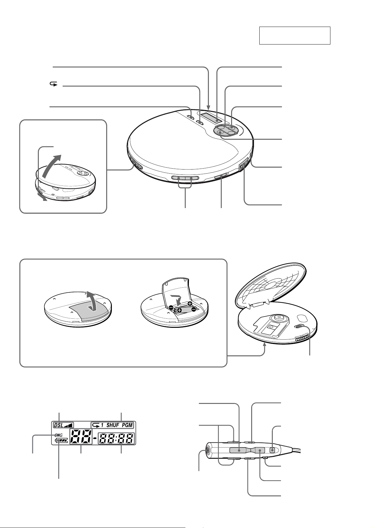
/
CD player (front)
SECTION 2
GENERAL
This section is extracted
from instruction manual.
Strap holes
1P-MODE/
2SOUND
A
OPEN
*The button has a tactile dot.
7VOL +*/–
6HOLD
Display
3r/t
(skip/search)
4ca *(play/
pause)/ENTER
5s(stop)/OFF
CHARGE
DC IN 4.5 V
(external power
input) jack
\ (headphones)
jack
CD player (rear/inside)
B
Open the battery
compartment lid.
Display
Sound mode
Play mode
Insert the ( end first (for both
batteries).
Remote control (XP-EV501R only)
4ca
7VOL
8E•A•S•S
3tF SKIP
2SOUND
CHG
Track number Playing time
Remaining battery power
Headphones
jack
6HOLD
5s
3rB SKIP
4
Page 5
Note : Disassemble the unit in the order as shown below.
SET
LOWER CABINET SECTION
XP-EV500/EV500N/EV501R
SECTION 3
DISASSEMBLY
CD MECHANISM SECTION
(CDM-3325ER)
MAIN BOARD
CABINET (FRONT) SUB ASSY
UPPER LID SUB ASSY
MOTOR ASSY (SLED) (M902),
OPTICAL PICK-UP (DAX-25E),
TURN TABLE MOTOR ASSY (SPINDLE) (M901)
5
Page 6

XP-EV500/EV500N/EV501R
Note : Follow the disassembly procedure in the numerical order given.
3-1. Lower Cabinet Section
3
six screws (B2)
2
two screws (B2)
5
Remove the cabinet (front) assy.
upper lid assy in the direction of
the arrow.
1
Open the battery lid.
8
switch unit assy (26P)
(CN301)
7
Remove the soldering.
When installing it,
align the switch position.
4
claw
9
lower cabinet section
6
hold knob
6
Page 7
)
3-2. CD Mechanism Section (CDM-3325ER)
4
three insulators
XP-EV500/EV500N/EV501R
5
CD mechanism
(CDM-3325ER )
1
connector (2P)
(CN403)
2
(CN402)
connector (4P
3
flexible board
(15P) (CN401)
7
Page 8

XP-EV500/EV500N/EV501R
3-3. Cabinet (front) Sub Assy
1
Remove the open left spring in
the direction of the arrow.
upper cabinet
2
open left spring
4
open right spring
3
Remove the open right spring in
the direction of the arrow.
upper cabinet
5
two claws
upper cabinet
6
Remove the upper lid assy in
the direction of the arrow.
7
cabinet (front) assy
8
Page 9

3-4. Upper Lid Sub Assy
y
XP-EV500/EV500N/EV501R
7
upper lid sub ass
5
1
seven screws
rubber
6
control button
4
liquid crystal display panel
3
switch unit assy
2
lid cover
9
Page 10

XP-EV500/EV500N/EV501R
p
3-5. MAIN Board
3
MAIN board
2
battery terminal board (relay)
1
Remove the soldering.
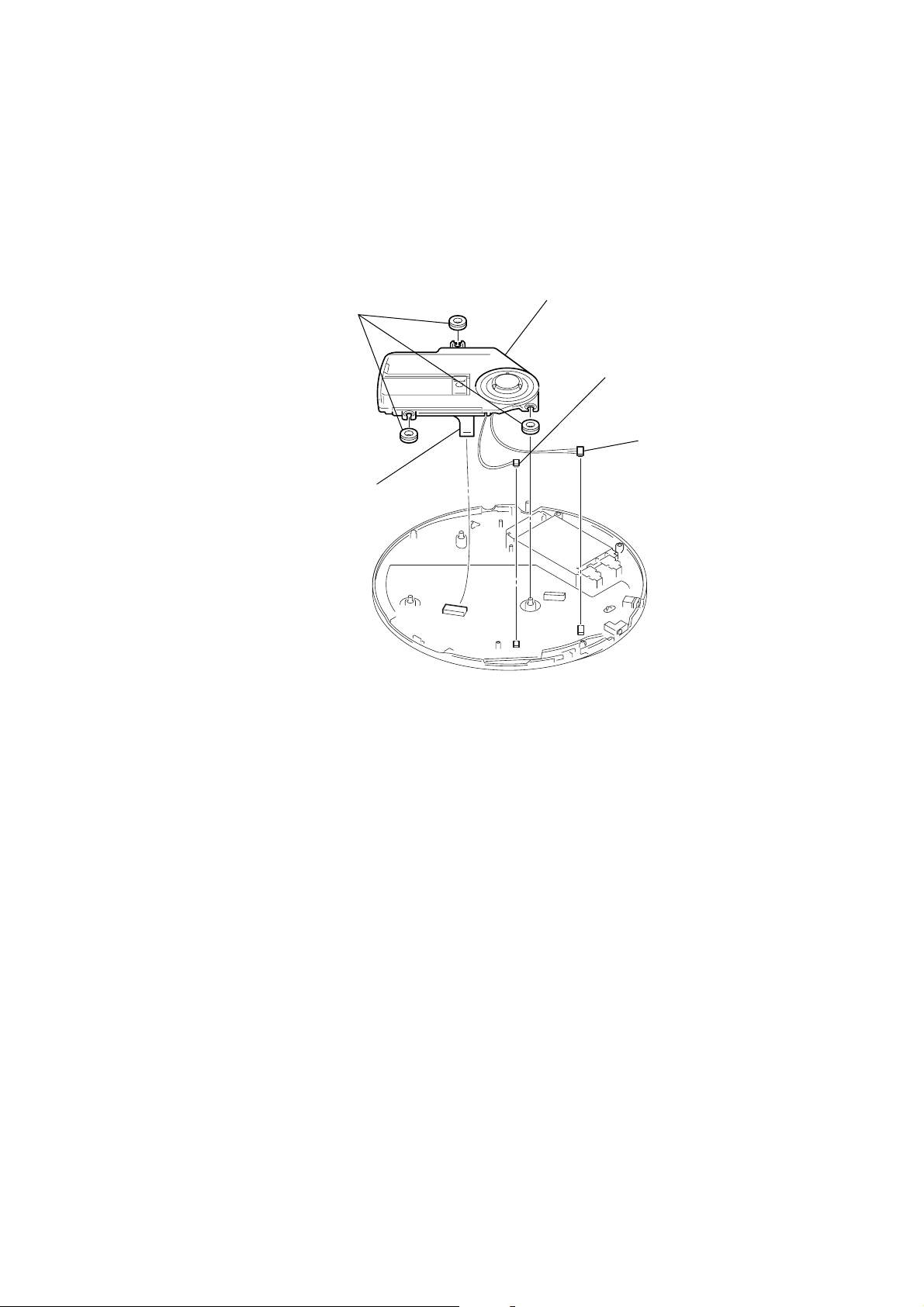
3-6. Motor Assy (sled) (M902), Optical Pick-up (DAX-25E), Turn Table Motor Assy (spindle) (M901)
1
three screws
(B1.7x4)
2
gear cover
3
motor assy
(sled) (M902)
5
three screws
(B1.7x4)
4
optical pick-u
(DAX-25E)
6
turn table motor assy
(spindle) (M901)
10
chassis
Page 11

SECTION 4
RF level
0.45 to 0.70 Vp-p
ELECTRICAL CHECKING
XP-EV500/EV500N/EV501R
The CD section adjustments are done automatically in this set.
In case of operation check, confirm that RF level.
Precautions for Check
1. Perform check in the order given.
2. Use YEDS-18 disc (Part No.: 3-702-101-01) unless otherwise
indicated.
3. Power supply voltage requirement : DC4.5 V in DC IN jack.
(J201)
VOLUME button : Minimum
HOLD switch : OFF
Checking Location:
– MAIN board (SIDE B) –
TJ403 (RF GND)
TJ401 (RF)
RF Level Check
Condition:
• Hold the set in horizontal state.
Connection:
oscilloscope
(AC range)
MAIN board
TJ401 (RF)
TJ403 (RF GND)
+
–
Procedure:
1. Connect the oscilloscope to the test points TJ401 (RF) and
TJ403 (RF GND) on the MAIN board.
2. Set a disc. (YEDS-18)
3. Press the u button.
4. Check the oscilloscope waveform is as shown below.
A good eye pattern means that the diamond shape (◊) in the
center of the waveform can be clearly distinguished.
RF Signal reference Waveform (Eye Pattern)
VOLT/DIV : 100 mV (With the 10:1 probe in use)
TIME/DIV : 500 ns
IC404
IC402
To watch the eye pattern, set the oscilloscope to AC range and
increase the vertical sensitivity of the oscilloscope for easy watching.
5. Stop revolving of the disc motor by pressing the x button.
11
Page 12

XP-EV500/EV500N/EV501R
SECTION 5
DIAGRAMS
NOTE FOR PRINTED WIRING BOARDS AND SCHEMATIC DIAGRAMS
Note on Printed Wiring Board
• X : parts extracted from the component side.
• Y : parts extracted from the conductor side.
• : Pattern from the side which enables seeing.
(The other layers' patterns are not indicated.)
Caution:
Pattern face side: Parts on the pattern face side seen from
(Side A) the pattern face are indicated.
Par ts face side: Parts on the parts face side seen from
(Side B) the parts face are indicated.
• MAIN board is multi-layer printed board. However, the patterns of intermediate-layer have not been included in the diagram.
Note on Schematic Diagram:
• All capacitors are in µF unless otherwise noted. pF: µµF 50 WV or
less are not indicated except for electrolytics and tantalums.
• All resistors are in Ω and 1/
•%: indicates tolerance.
• C : panel designation.
The components identified by mark 0 or
dotted line with mark 0 are critical for safety.
Replace only with part number specified.
• A : B+ Line.
•Total current is measured with CD installed.
•Power voltage is dc 4.5 V and fed with regulated dc power supply
from DC IN jack (J201).
•Voltages and waveforms are dc with respect to ground in playback
mode.
no mark : CD PLAY
•Voltages are taken with a VOM (Input impedance 10 MΩ).
Voltage variations may be noted due to normal production tolerances.
•Waveforms are taken with a oscilloscope.
Voltage variations may be noted due to normal production tolerances.
• Circled numbers refer to waveforms.
• Signal path.
J : CD PLAY (ANALOG OUT)
4
W or less unless otherwise specified.
• WAVEFORMS
1 IC401 if RFAC
100mV/DIV, 400ns/DIV
600 mVp-p
2 IC402 rk XTAO
1V/DIV, 20ns/DIV
2.7 Vp-p
59ns
3 IC301 2 XIN
1V/DIV, 100ns/DIV
236ns
2.8 Vp-p
4 IC301 qk MSCK-O
1V/DIV, 400ns/DIV
12
932ns
2.3 Vp-p
Page 13

5-1. Block Diagram
XP-EV500/EV500C/EV500N/EV501R
OPTICAL PICK-UP
BLOCK
(DAX-25E)
VR
FOCUS
C0IL
TRACKING
COIL
M902
SLED
MOTOR
OPG SW
M901
SPINDLE
MOTOR
VCC
M
OP STB
LD
GND
PD
DIGITAL SERVO
DSP
MEMORY CONT/
DIGITAL HI & BUS BOOST
100
103
104
102
IC402
A OUT1
84
RFAC
88
RFDC
92
A
91
B
89
E
90
F
XTAI
47
XTAO
48
FFDR
96
FRDR
95
TFDR
98
97
TRDR
SFDR
SRDR
99
MDP
SYNC
MDS
A OUT2
LRMU
DOUT
A10
XWE
XRAS
XCAS
SQTO
CLOK
XLAT
XSOE
SENS
SCOR
FOK
R4M
SYSM
XRST
51
56
61
62
116
113
.
17
A0
15
.
13
11
2
1
9
4
.
D0
3
.
6
D3
.
5
21
20
23
24
22
27
65
32
25
28
16M DRAM
9
12
.
15
19
A10
.
21
.
8
XWE
4
XRAS
5
XCAS
23
IC404
A0
OPEN
HOLD
ESP
MSDTO
MSCK
MXLAT
XSOE
MSDTI
SCOR
FOK
XIN
AMUTE
XRST
XPOWLT
AD KEY
AD KEY2
SEG0
SEG14
COM0
COM3
µCON
IC301
PWR SW
AD-SEL
AD_RMKEY
TSB_I/O
AD DC IN MNT
AD BATT MNT
CHG MNT
DC ON
BEEP
30
74
24
26
31
27
22
21
70
2
.
D0
3
.
24
D3
.
25
SWITCH UNIT
LIQUID CRYSTAL DISPLAY
&
LCD
(OPEN/CLOSE)
S304
HOLD
S305
E·A·S·S
S303
ON
OFF
2
1
VCPU2,0V
S302
-
S301
VCPU+2V
+
VOL
28
40
38
17
18
15
14
16
11
9
2
13
79
75
25
23
56
42
60
57
VCC2
RF
A
B
E
F
APC
Q207
F+
F-
T+
T-
S+
S-
MOTOR/COIL DRIVE
IC201(1/2)
SEO
22
SEM
23
FO2
48
RO2
46
FO3
44
RO3
42
FO1
52
RO1
50
COM
80
UO2
2
VO2
4
WO2
6
PWM
SYNC
BBK
DATA
CLOCK
XRST
LATCH
RESET
RI2
RI3
RI1
X402
FI2
58
57
FI3
60
59
FI1
56
55
IC401
3
4
72
34
70
39
38
36
40
FG
74
35
1
HEADPHONE AMP
IC701
14
L OUT
L IN
15
R OUT
R IN
18
MUTE
17
BEEP
20
PWR SW
VCPU 2,0V
VCC2
J701
8
6
B+
POWER CONTROL
IC201(2/2)
18
Q206
19
66
67
24
37
VCC2
VCPU2.0V
VM MNT
CHG MNT
SEP
WAKE UP
VIN
DC INS
SP VCC1
SP VCC2
VM1
VM12
VM23
VM3
BATM1
DET
CHG B
VCCO
VCC
STNG
REG B
DC IN
LG
12
64
53
49
45
41
68
63
65
20
16
25
62
61
8
1
5
EXCEPT EV501R
DC DET
Q201
REG
Q203
D206
EV501R
Q204
Q202
D202
D204
DRY BATTERY
SIZE "AA"
(IEC DESIGNATION LR6)
2PCS, 3.0V
J201
DC IN 4.5V
:CD PLAY (ANALOG OUT)
72
78
77
8
FG
OPG SW
OP STB
RESET
1313
Page 14

XP-EV500/EV500C/EV500N/EV501R
Ver 1.2 2003.08
5-2. Printed Wiring Board – MAIN Board (SIDE A) –
A
B
C
D
E
F
G
H
12
J701
2
EXCEPT EV501R
EV501R
VDR701
34567891011
MAIN BOARD (SIDE A)
M901
SPINDLE MOTOR
FB704
R717
L701
EV501R
L203
L201
C205
VDR201
C207
D203
C210
C719
EV501R
C206
TP412
VDR703
VDR202
(COM)
C722
TP412
VDR702 VDR704
FB702
R718
L202L204
4
(U)
1
C721
R715
FB701
R719
EV500/EV501R
R209
S304
HOLD c
CN402
FB703
R716
R210
R208
C212
D202
SWITCH
LIQUID CRYSTAL
DISPLAY
ON OFF
TP411
TP411
(M)
C221
+
&
12 13 14
VOL
S301
+
25
26
R307
C227
C306
TAP301
(VL)
TP302
(BEEP)
R319
R214
IC201
20 21
6061
TP201
(DC+)
TP310
(HPSW)
TP413 (S+)
TP204
(DC+)
C228
+
TP414 (S-)
1
CN403
41
40
TP203
(DC+)
SL302
(VL)
TP309
TAP302
(VL)
TAP303
(VL)
(VL)
C238
C239
M902
SLED MOTOR
C214
C216
C215
C217
C218
C219
R213
L209
(V)
1
2
L206
C220
CN301
R316
80
1
L207
+
SL303
(VL)
R311
R313
R314
R302
R301
SL701
(VL)
TP308
(VL)
C240
R712
S302
R223R226
C714
TP388
(OPTOUT)
-
L210
C229
R228
Q207
+
TP304
(OPGSW)
L208
L211
C718
S303
(OPEN/CLOSE)
L212
TP701
(LCH)
TAP304 (VL)
C322
R339
TJ305 (OPEN)
E A S S
SL202
(VL)
C717
TP702
(RCH)
S305
+
2
D301
TP422 (VL)
1
TP417 (VL)
TP402 (T+)
TP401 (F+)
TP406 (F-)
TP402 (T-)
R341
1
CN401
TP421 (VL)
TP444 (VL)
R423
R410
TP420 (VL)
TP418 (VL)
IC401
4
5
C406
C402
15
TP419 (VL)
R404
3
1
L401
C404
R402
C403
R405
R408
L405
R444
D401
D402
EV500:AEP,UK
/EV500C/EV500N
R409
C433
SL401
(VL)
/EV501R
C428
OPTICAL
PICK-UP
BLOCK
(DAX-25E)
• Semiconductor
Location
Ref. No. Location
D202 F-4
D203 H-3
D301 E-10
D401 C-13
D402 D-13
IC201 C-7
IC401 D-12
Q207 D-9
I
1414
Page 15

5-3. Printed Wiring Board – MAIN Board (SIDE B) –
XP-EV500/EV500C/EV500N/EV501R
Ver 1.2 2003.08
A
B
C
D
E
F
G
H
12
34567891011
12 13 14
• Semiconductor
MAIN BOARD (SIDE B)
TP443
(SFDR)
TP442
(SRDR)
TP440
(TRDR)
TP438
(FRDR)
TJ304
(G-PRO)
TJ403
TP407
TP405
(F)
TP426
(VL)
C430
C440
C432
C439
1
26
(RF GND)
(A)
TP408
(B)
R413
R421
R414
R429
R415
R416
R433
C420
C413
TP416
TP404
C412
(VL)
(E)
TP415
(VL)
C421
C417
R412
TP425
(VL)
TJ402
IC402
IC403
IC404
C437
C436
R441
13
IC403:EV500C/EV500N:CND, E
IC404:EXCEPT:EV500C/EV500N:CND, E
I
14
R440
R439
R437
R443
R438
R442
C435
TP433
(VL)
R436
(LD)
C409
TJ401
(RF)
R427
R411
R432
L404
C411
R428
C416
C418
TP437
(VL)
TP441
(TFDR)
TP439
(FFDR)
C415
TP431
(VL)
TP430
C408
C419
C431
(VL)
R418
R419
C410
C407
R420
R431
R426
TP423
R434
C434 R435
(VL)
L403
R425
X401
C708
TP424
(VL)
C706
C709
R720
C710
C414
L213
C429
L214
C424
R707
R750
C423
IC701
R704
C702
C422
C425
L402
R706
R702
C750
C751
(XRST)
TJ303
R705
R701
C701
R751
EV500C/EV500N
R334
R332
R229
TP703
/EV501R
C234
(VL)
R714
SL201
(VL)
R220
R708
C715
C712
R703
R324
EV500C/EV500N
/EV501R
TJ207
(VCC2)
R312
C316
C713
R222
C716
R709
C320
R326
C233
C321
R327
R328
SL203
(VL)
TP306
C319
FB206
(VL)
C317
SL301
(VL)
R337
C310
C231
R325
R323
R227
R233
TJ301
(PWRSW)
Q206
FB207
C311
C304
FB205
C235
TJ208
(VCPU)
R321
C237
R221
(D GND(uCOM))
R322
C303
IC301
C302
R212
R218
D207
R234
TP301
R320
C301
R217
R309
R315
TP303
(VL)
C223
R308
Q204
C315
C222
R310
C225
C313
C230
C314
R303
C226
R306
C224
(D GND(DSP))
R304
C312
R305
L205
TP202
TJ203
(BATC)
TJ210
(AU GND)
L215
FB203
FB204
Q203
TJ209
(A GND)
FB202
R215
D205
C211
R216
TJ307
(HOLD)
R340
Q202
D206
R211
B
C
E
R206
R205
D204
Q201
C208
TJ206
(MAIN GND)
TJ202
(B+)
R207
BT201
TJ205
(DC+)
TJ703
(HP GND)
TJ702
(HP L OUT)
BT202
TJ704
(RM KEY)
BT203
TJ701
(HP R OUT)
TJ204
(B-)
Location
Ref. No. Location
D204 F-11
D205 E-10
D206 E-10
D207 C-8
IC301 G-8
IC402 G-4
IC404 H-2
IC701 E-6
Q201 E-11
Q202 F-11
Q203 E-10
Q204 D-9
Q206 C-8
J201
DC IN 4.5V
DRY BATTERY
SIZE "AA"
(IEC DESIGNATION LR6)
2PCS, 3.0V
1515
Page 16

XP-EV500/EV500C/EV500N/EV501R
Ver 1.2 2003.08
5-4. Schematic Diagram – MAIN Board (1/4) –
CN401
15P
TP404
TP405
E+
T-
TP401
TP402
• See page 12 for Waveforms. • See page 20 for IC Block Diagrams.
TP419
TP420
TP421
C420
R431
R432
TP422
TP423
TP424
470p
TP407
TP408
TJ401
TJ402
T+
TP403
F-
TP406
C414
2.2k
R418
R420
10k
C411
0
2200p
R427
47k
22k
22k
R421 R429
C412
C413 C421
0.1
R425
2.2k
C415
0.47
470k
R428
C416
100p
2200p
C417 C418 C419
22p 474V0.1
100k 100k
470p
470p 470p
(RF)
TJ403
RF GND
C402
4.7
MA111-TX
47k
D401
R402
SL401
R404
R410
470k
R405
0
D402
MA111-TX
22k
R409
22k
4.7
R408
C403
C404
47p
IC401
TC75S57F(TE85R)
C406
R423
0.1
4.7
0
0.1
C407
C408
4700p
C410
0.47
1M 220k
R419 R426
R411
C409
R412
R413
TP415
22k
R414
22k
R415
TP416
22k
R416
10k
TP417
TP418
47k
TP425
TP426
C422
6.3V
R720
47
C423 C424
47
0.1 0.1
FFDR
FRDR
TP439
TP438
TRDR
TP440
TFDR
TP441
4V
47
C425
SRDR
TP442
SFDR
TP443
X401
16.934MHz
IC402
CXD3048R
TP427
C428
R435
2.2k
1
L402
C431
0
L403
C429
TP428
R433
100
4V
0.1
220
R434
TP430
TP432
TP431
TP429
0
C440
0.1
C430
C432
0.1
0.1
TP433
L404
C433L401
47
6.3V
R436
100k
C434
47p
R437
R438
R439
R440
R441
R442
C436
TP434
TP435
TP436
TP437
R443C435
100k0.47
0
0
0
0
0
0
100p
C437
0.1
L405
R444
0
(Page 17)
/EV500C
(Page 18)
(Page 19)
1616
Page 17

5-5. Schematic Diagram – MAIN Board (2/4) –
IC404
MSM51V17400F -10TK-FS
(Page 16)
• See page 20 for IC Block Diagrams.
EXCEPT:EV500C/EV500N:CND, E
1
C439
R751
4.7k
TP701
LCH
C750
470p
R750 R702 R704
TP702
4.7k 22k 47k
RCH
A9
C751
470p
C701
2.2
C702
2.2
SL701
XP-EV500/EV500C/EV500N/EV501R
Ver 1.2 2003.08
10p
VDR704
10p
C721
C722
J701
FB704
R716
470
R715
L701
R717
470
FB701
FB702
FB703
C719
R718
0
0
VDR702
TJ703
10k
VDR701
TJ701
HP R OUT
HP GND
VDR703
TJ702
HP L OUT
TJ704
RM KEY
R719
1k0.001
TP703
C709
0.47
C712
0.1
C713
22
R714
6.3V
0
R703R701
47k22k
R705
22k
*1
R706
22k
*1
0.1
C706
C708
22
6.3V
C710
22
6.3V
IC701
TA2120FN(EL)
R707
4.7
C714
47
6.3V
R708
4.7
R712
R709
4.7
0
C715
0.1
C716
0.1
C717
220 4V
C718
220 4V
IC403
IC41UV4105-100T
EV500C/EV500N:CND, E
C322
TJ305
4700p
3
-
TJ304
G-PRO
R339
220k
R340
R341
0
0
OPEN
TJ307
HOLD
TAP304
S303
S304
S305
(Page 19)
1717
Page 18

XP-EV500/EV500C/EV500N/EV501R
5-6. Schematic Diagram – MAIN Board (3/4) –
CN403
2P
CN402
4P
• See page 20 for IC Block Diagrams.
TP409
U
TP410
V
TP411
W
TP412
COM
470
R211
Q202
2SB1237TV2PQR
Q201
2SD1781K-T146-QR
100
R207
D204
MA2YD2300LS0
1
2.2
206
R205
TJ205
R
R212
DC+
0
C208
4.7
TP414
TP413
2SC4116GL-TE85L
C215
C216
C217
C218
C219
D206
MA111-TX
Q203
4700pB
4700pB
4700pB
R213
22k
0.022
0.022
C214
R214
(Page 16)
V
6.3
10
C229
L2
220
08
L2
215
R
100k
216
R
100k
0
IC201
L206
BH6580KV
7
20
L
C222
4.7
R217
0
C226
C223
C225
470p
209
L
1
1
1
L205
C220
220 6.3V
Q204
2SB167900LSO
TP201
DC+
L211
TP203
C233
0
2
U
P
CC
C
V
V
07
J208
TJ2
0
FB205
T
0
B206
F
0
7
FB20
(Page 19)
2200p
TP204
R220
R222
R229
4.7
C234
10 4V
R227
R228
10k
2.2k
Q206
2SC4081T106
R221
10k
0
0
MA111-TX
C235
Q207
2SB167900LSO
k
00
1
3
R226
22
2.2
R
D207
0.22
01
L2
S
1000p
C238
0.047
C239
SL202
C240
0.1
L212
1
237
C
03
L2
S
R234
R233
470k
100k
J201
BT201
BT202
BT203
D202
MA2H735-(TX).SO
TJ202
B+
TJ203
BATC
TJ204
B-
C206
1000p 0.22
L203L201 R210R208
0 47k100k
VDR202
L202
0
C205
L204
1
201
R
D
V
C207
1
1
1
211
210
C
C
O
203
D
735-(TX),S
A2H
M
C212
R209
V
V
V
V
.3
4V
0
7
4
4
1
4
6
24
23
22
228
23
0
C2
C
C
7
C
47
47
C
4
22
100k
R218
D205
UDZSTE
-175.1B
C221
TJ206
22k
MAIN_GND
220 6.3V
100
1818
Page 19

XP-EV500/EV500C/EV500N/EV501R
5-7. Schematic Diagram – MAIN Board (4/4) –
• See page 12 for Waveforms.
(Page 16)
C301
4700p
C310
4700p
C302
4700p
C311
4700p
C304
4700p
C306
R313
100k
4700p
0
R301
100k
R314
0
R302
100k
R305
100k
R306
100k
R307
100k
R308
(Page 17)
1M
R315
TP302
TP303
BEEP
0
R319
0
R320
0
R321
0
R323
100k
R310
0
R325
0
R326
100k
R327
R312
C316
C317
R324
22k
4700p
0.01
22k
SL301
R328
47k
C321
0.01
(Page 18)
0
L213
0
FB202
A_GND
TJ209
0
L214
AU_GND
TJ210
0
L215
0
FB203
D_GND(DSP)
TP202
0
FB204
TP301
D_GND(UCOM)
R304
0.1
C312
C313
R332
0
TP308
TP309
TP310
IC301
T5AW5-C7
TP306
4V
22k
1k
1k
R311
R316
R309
10
C303
0
R322
PWRSW
TJ301
0.22
C315
C314
0.1
0.1
R303
100k
100k
OPSTB
TJ302
OPGSW
TP304
ST
XR
TJ303
S301
S302
C320C319
0.10.22
MA2ZD14001S0
SL302
R334
D301
0
R337
10k
TAP301
TAP303
TAP302
SL303
CN301
26P
1919
Page 20

XP-EV500/EV500C/EV500N/EV501R
5-8. IC Block Diagram
DCIN
REGB
DET
DCIN S
CHGB
VMMNT
CHGMNT
BATM1
BATM2
BRK
PREGND
PWM
SOFTPWM
CSL2
CSL1
COM
IC201 BH6580KV
FERFDC
AVSSO
IGEN
AVDD0
RFAC
AVDD3
BIAS
ASY_I
VM23
RO2
FO247PGND2
CH1
VCC3
VM12
RO1
49
5052
VG
4648
CH2
H BRIDGE
CLK
SAWGEN
45
VCC
H BRIDGE
−
+
VCC
FIN3
59
60
HV PROT
61
CONTROLLER
62
63
64
65
CHARGE
66
67
MONITOR
INPUT
SELECT
SLOPE
SIGNAL
+
−
+
−
+
−
AMP
LOGIC
PRE DRIVE
68
69
70
71
72
73
FG
74
75
76
WI
77
VI
78
UI
79
80
55
58
DGND
54
LEVEL
SHIFT
VG
FO151PGND1
VM1
53
H BRIDGE
VGVCC
VM
VG
RIN156FIN157RIN2
FIN2
RIN3
CH3
−
+
VG
VCC4
VM3
4244
41
INTERFACE
RESET
10m SEC
DELAY
−
+
−
+
VCC2
40 LATCH
39 DATA
38 CLOCK
37 WAKEUP
36 XRST
35 RSTOUT
34 SYNC
33 PREGND
32 SOFT
31 SLOW
30 EI
29 EO
28 VCC2NF
27 VCPUNF
26 PMG
25 STNG
SEP
2324SEM
22 SEO
21 GSW
VCC
VSS2
FRDR
FFDR
TRDR
TFDR
SRDR
SFDR
SSTP
MDS
MDP
SYNC
VDD2
LRCK_O
LRCK_I
PCMD_O
PCMD_I
BCK_O
BCK_I
DVDD
A10
A11
A12
A13
91
B
92
A
93
VC
94
95
96
97
98
99
100
101
MDS
102
103
104
SYNC
105
VDD
106
107
108
109
110
111
112
VDD
113
A3
114
A2
115
A1
116
A0
117
118
119
TEST
3, 4
120
90
ANALOG SW
FOCUS
PWM
TRACKING
PWM
SLED
PWM
8768
89
A/D
DIGITAL
CLV
SELECTOR
SERVO
INTERFACE
CONTROLER
86
838485
AVDD
ASYMMETRY
CORRECTOR
SERVO DSP
PWM GENERATOR
MEMORY
RO3
FO343PGND3
ASY_O
81
7980
82
D/A
SEQUENCER
IC402 CXD3048R
AVSS3
ERROR
CORRECTOR
INTERFACE
SERVO
AUTO
32K
RAM
SUB CODE
PROCESSOR
78
VPCO
77
CVTL
CVTV
FILO
EFM
DEMODULATOR
FILI
747576
DIGITAL
PLL
73
PCO
VDD
VDDI
XPCK
7172
DIGITAL
OUT
XUGF
GFS
6970
INTERFACE
68
CZPO
CPU
COUT
6667
MIRR
DAC
65
MIRR
DFCT
FOK
FOK
DFCK
6364
ATSK
62
DOUT
LRMU
61
LPF
LPF
CLOCK
GENERATOR
AVDD
AVDD
VDD
VDD
TEST
TES1
R4M
VSSI
60
TEST
59
TEST1
58
AVDD2
57
AOUT2
56
VREFR
55
AVSS2
54
AVSS1
53
VREFL
52
AOUT1
51
AVDD1
50
XVSS
49
XTAO
48
XTAI
47
XVDD
46
HPVDD
45
HPR
44
HPL
43
HVSS
42
XTSL
41
EXCK
40
SBSO
39
XWIH
38
XEMP
37
SQSO
36
SCLK
35
BQCK
34
VSS0
33
R4M
32
XWRE
31
SPVCC
21
U_OUT
3
SPGND
4
V_OUT
5
SPVCC
6
W_OUT
7
SPGND
TEST
1312
1110
9VG8
LG
SSW
VCC3
VIN
DSW
14
POWGND
15
16
USW
VCC017VCC118VCC2
19
VCPU
20
VCC
1
2
XRAS
3
XWE
4
D1D0D3
1, 2
8
5
6
9
10
DCKE
XCAS
WFCK/DOM
11
A9A8A7
7
D2
DCLK
15
14
12
13
DVSS
17
16
A6A5A4
VDD
181920
XRDE
VDD0
CLOK
212223 24 25 26 27
XLAT
SENS
XSOE
SDTO
SYSM
WQCK
28 29
SCOR
XRST
XRST
30
PWMI
XQOK
IC701 TA2120FN (EL)
BSTO
24
BST
+
ADDB
BB
BIASI
SW
23
–
ADD
22
BIAS
A
BIAS
21
PWC
SW
PWR
SW
20 19
PWSWMT
BEEPMUTE MUTEC
18
17
ROUT
PW
C
BEEP
+
PW
LOUT
–
A
SW
+
–
PW
B
16
15
ALC ALC
ATT
LINRINGND
13
14
ATT
SW
ALC
DET
1
BSTNFADD
OUT
4
2
3
RF IN OCL ROUT VREF LOUT PGND MIXO ALCINALC
5
VCC
7
6
8
10
11
9
12
DET
2020
Page 21

5-9. IC Pin Function Description
• IC301 T5AW-C7 (µCON)
Pin No.
1
2
3
4
5
6
7
8
9
10
11
12
13
14
15
16
17
18
19
20
21
22
23
24
25
26
27
28
29
30
31
32
33
34
35
36
37
38
39
40
41
42 to 56
57 to 60
61 to 65
66
67
68
69
70
71
Pin Name
GND
XIN
XOUT
TEST
VDD1
DRAM_SEL_I
NC
RESET_I
FOK_I
NC
SCOR_I
GRSCOR_I
AMUTE_O
XSOE_O
XLAT_O
MSDTI_I
MSDTO_O
MSCK_O
AVDD
ADVREF
AD_CHGMNT
AD_BATMNT
AD_KEY2
AD_SEL
AD_KEY
AD_RMKEY
AD_DCINMNT
CLOSE
PPG
BEEP_O
TSB_I/O
VDD_EEPROM
EXTBATT_I
TEXTSKIP_I
DIG_TU_I
RCHG2/1_I
XSTAND_ON_I
ESP_I
AVLS_I
HOLD_I
SEG15
SEG14 to SEG0
COM3 to COM0
V3 to V1,C1,C0
XWAKEUP_O
PGM_SDTO
PGM_SDTI
PGM_SCK_O
CD-ON
GFS_I
I/O
—
Ground (digital)
I
System clock input from CXD3048R(IC402)
O
Not used
I
Test pin (normally connected to ground)
—
Power supply (digital +2V)
I
4M/64M DRAM select pin (connected to VDD1)
O
Not used
I/O
System reset signal input from the power control(IC403) (“L”:reset)
I
Focus OK signal input from CXD3048R(IC402) (“L”:NG, “H”:OK)
I
Not used
I
Subcode sync detection signal input from CXD3048R(IC402)
I
GRSCOR signal input from CXD3048R(IC402)
O
Analog muting ON/OFF control signal output (“H”:muting ON)
O
Serial data output enable signal output
O
serial data latch pulse signal output to CXD3048R(IC402)
I
Serial data input to CXD3048R(IC402)
O
Serial data output to BH6580KV-F(IC201) and CXD3048R(IC402)
O
Serial data transfer clock output to BH6580KV-FCXD3029R(IC601)
—
Power supply (analog +2V)
—
AD converter port standard voltage (connected to AVDD)
I
Battery charging voltage detection signal input from BH6580KV-F(IC201)
I
Battery voltage detection signal input
I
Key input terminal
I
Optical out plug in detection signal input
I
Key input terminal
I
Remote control key input
I
DC IN voltage detection input terminal also using detection of DC IN existence
I
CD DOOR OPEN/CLOSE detection switch(S303) signal input
O
Not used
O
Beep sounds output terminal to TA2120FN(IC701)
I/O
Communication data bus input or output to the remote control (Not used)
—
Not used
I
Not used
I
Not used
I
Not used
I
Not used
I
Not used
I
E•A•S•S switch(S305) input (“H”:2, “L”:1)
I
Not used
I
KEY HOLD switch(S304) input terminal
O
Not used
O
LCD segments drive signal output
O
LCD common drive signal output
O
Capacitor connection terminal for LCD drive voltage step-up
O
WAKE-UP control signal output (signal for reset the condition of the system stand-by) (“L”:Wake)
O
Not used
I
Not used
O
Not used
O
AGC control pulse output to BH6580KV-F(IC201)
I
Not used
XP-EV500/EV500N/EV501R
Description
21
Page 22

XP-EV500/EV500N/EV501R
Pin No.
72
73
74
75
76
77
78
79
80
Pin Name
FG_I
PGMSEL_O
PWRSW_O
XPOWLT_O
CHGGND_SL_I
XOPSTBY_O
OPGSW_O
XRESET_O
C2POEN_O
I/O
I
FG pulse signal input from BH6580KV-F(IC201)
O
Not used
O
Power supply control output of TA2120FN(IC701) (“H”:ON)
O
Latch signal output to BH6580KV-F(IC201)
I
Not used
O
Optical-pick up voltage control output (“H”:gain up)
O
RF AMP gain control output (“H”:gain up)
O
Reset signal output to BH6580KV-F(IC201) and CXD3048R(IC402)
O
Not used
Description
22
Page 23

NOTE:
• -XX and -X mean standardized parts, so they
may have some difference from the original
one.
• Items marked “*” are not stocked since they
are seldom required for routine service. Some
delay should be anticipated when ordering these
items.
6-1. Cabinet Upper Section
6
5
4
17
XP-EV500/EV500C/EV500N/EV501R
SECTION 6
EXPLODED VIEWS
• The mechanical parts with no reference number in the exploded views are not supplied.
• Accessories and packing materials are given
in the last of the electrical parts list.
•Abbreviation
AUS: Australian model
CND : Canadian model
E18 : 100 – 240 V AC area in E model
E33 : 100 – 240 V AC area in E model
HK : Hong Kong model
MX : Mexican model
12
7
8
16
The components identified by mark 0 or
dotted line with mark 0 are critical for safety.
Replace only with part number specified.
not supplied
14
Ver 1.2 2003.08
11
13
19
not supplied
15
3
2
1
18
5
cabinet lower section
Ref. No. Part No. Description Remarks Ref. No. Part No. Description Remarks
1 3-249-061-01 DETECTOR, LEVER
2 3-249-062-01 KNOB, OPEN
3 3-249-069-01 SPRING, TENSION
4 X-3382-960-1 CABINET (FRONT) SUB ASSY (EV500)
4 X-3382-968-1 CABINET (FRONT) SUB ASSY
(EV500C/EV500N:CND, E, AEP)
4 X-3383-448-1 CABINET (FRONT) SUB ASSY (EV501R)
5 3-245-862-31 SCREW (B2), TAPPING
6 A-3608-206-A LID SUB ASSY, UPPER (EV501R)
6 X-3382-954-1 LID SUB ASSY, UPPER (EV500N)
6 X-3382-959-1 LID SUB ASSY, UPPER (EV500)
6 X-3383-161-1 LID SUB ASSY, UPPER (BLUE)(EV500N:AEP)
6 X-3383-162-1 LID SUB ASSY, UPPER (BLACK)(EV500N:AEP)
6 X-3383-163-1 LID SUB ASSY, UPPER (BLUE)(EV500:AEP)
6 X-3383-166-1 LID SUB ASSY, UPPER (BLACK)(EV500:AEP)
6 X-3383-168-1 LID SUB ASSY, UPPER (EV500C)
6 X-3383-875-1 LID SUB ASSY, UPPER (EV500N:CND)
7 3-249-067-01 SPRING, FULL OPEN.LEFT
8 3-249-068-01 SPRING, FULL OPEN.RIGHT
11 3-249-057-01 BUTTON, CONTROL
12 3-249-070-01 RUBBER
13 1-805-122-11 DISPLAY PANEL, LIQUID CRYSTAL
14 1-477-704-11 SWITCH UNIT
15 3-355-424-81 SCREW, TAPPING
16 3-249-060-01 KNOB, EASS
17 3-254-579-01 CUSHON, CABI
18 3-254-876-01 SHEET PLATE, ADHESIVE
19 3-255-548-01 SHEET, SHILD
23
Page 24

XP-EV500/EV500C/EV500N/EV501R
Ver 1.2 2003.08
6-2. Cabinet Lower Section
52
not supplied
53
57
61
CD mechanism deck section
(CDM-3325ER)
52
61
not supplied
58
59
60
Ref. No. Part No. Description Remarks Ref. No. Part No. Description Remarks
52 3-245-331-02 INSULATOR
* 53 A-3347-855-A MAIN BOARD, COMPLETE (EV500N:AEP)
* 53 A-3347-900-A MAIN BOARD, COMPLETE
(EV500:E18, E33, HK, MX, AUS)
* 53 A-3663-994-A MAIN BOARD, COMPLETE
(EV500C/EV500N:CND, E)
* 53 A-3683-306-A MAIN BOARD, COMPLETE (EV500:AEP, UK)
* 53 A-3683-556-A MAIN BOARD, COMPLETE (EV501R)
57 3-249-066-01 TERMINAL BOARD (RELAY), BATTERY
58 3-249-054-01 CABINET, LOWER (EV500/EV500C/EV500N)
58 3-249-054-21 CABINET, LOWER (EV501R)
59 3-249-059-01 KNOB, HOLD
60 3-249-055-01 LID, BATTERY
61 3-254-581-01 CUSHON, COMTACT
24
Page 25

6-3. CD Mechanism Deck Section (CDM-3325ER)
2
104
M901
XP-EV500/EV500C/EV500N/EV501R
101
102
109
110
108
106
107
111
105
M90
103
101
Ref. No. Part No. Description Remarks Ref. No. Part No. Description Remarks
101 3-318-203-61 SCREW (B1.7X4), TAPPING
0 102 X-3380-950-1 OPTICAL PICK-UP (DAX-25E)
103 3-221-473-01 COVER, GEAR
104 3-221-472-02 CHASSIS
105 3-221-474-01 SPRING, SLED
106 A-3180-967-A FEED ASSY, SCREW
107 3-221-268-01 GEAR (B)
108 3-221-475-01 SHAFT, STANDARD
109 3-222-298-01 RACK
110 3-222-299-01 SPRING, RACK RETAINER
111 3-348-998-31 SCREW (M1.4X2.5), TAPPING, PAN
M901 A-3180-965-A MOTOR ASSY, TURN TABLE (SPINDLE)
M902 A-3180-966-A MOTOR ASSY, SLED (SLED)
The components identified by mark 0 or
dotted line with mark 0 are critical for safety.
Replace only with part number specified.
25
Page 26

XP-EV500/EV500C/EV500N/EV501R
Ver 1.2 2003.08
MAIN
ELECTRICAL PARTS LIST
SECTION 7
NOTE:
• Due to standardization, replacements in the
parts list may be different from the parts specif
ied in the diagrams or the components used
on the set.
• -XX and -X mean standardized parts, so they
may have some difference from the original
one.
• RESISTORS
All resistors are in ohms.
METAL: Metal-film resistor.
METAL OXIDE: Metal oxide-film resistor.
F: nonflammable
Ref. No. Part No. Description Remarks Ref. No. Part No. Description Remarks
* A-3683-306-A MAIN BOARD, COMPLETE (EV500:AEP, UK)
*********************
* A-3683-556-A MAIN BOARD, COMPLETE (EV501R)
*********************
* A-3347-855-A MAIN BOARD, COMPLETE (EV500N:AEP)
*********************
* A-3663-994-A MAIN BOARD, COMPLETE
*********************
* A-3347-900-A MAIN BOARD, COMPLETE
*********************
3-249-064-01 TERMINAL BOARD (+), BATTERY
3-249-065-01 TERMINAL BOARD (-), BATTERY
• Items marked “*” are not stocked since they
are seldom required for routine service.
Some delay should be anticipated when ordering these items.
• SEMICONDUCTORS
In each case, u: µ, for example:
uA. . : µA. . uPA. . : µPA. .
uPB. . : µPB. . uPC. . : µPC. .
uPD. . : µPD. .
• CAPACITORS
uF: µF
• COILS
uH: µH
(EV500C/EV500N:CND, E)
(EV500:E18, E33, HK, MX, AUS)
•Abbreviation
AUS:Australian model
CND : Canadian model
E18 : 100 – 240 V AC area in E model
E33 : 100 – 240 V AC area in E model
HK : Hong Kong model
MX : Mexican model
The components identified by mark 0 or
dotted line with mark 0 are critical for safety.
Replace only with part number specified.
When indicating parts by reference number,
please include the board name.
C238 1-162-964-11 CERAMIC CHIP 0.001uF 10% 50V
C239 1-165-176-11 CERAMIC CHIP 0.047uF 10.00% 16V
C240 1-164-156-11 CERAMIC CHIP 0.1uF 25V
C301 1-162-968-11 CERAMIC CHIP 0.0047uF 10% 50V
C302 1-162-968-11 CERAMIC CHIP 0.0047uF 10% 50V
C303 1-135-201-11 TANTALUM CHIP 10uF 20% 4V
C304 1-162-968-11 CERAMIC CHIP 0.0047uF 10% 50V
C306 1-162-968-11 CERAMIC CHIP 0.0047uF 10% 50V
C310 1-162-968-11 CERAMIC CHIP 0.0047uF 10% 50V
C311 1-162-968-11 CERAMIC CHIP 0.0047uF 10% 50V
C312 1-164-156-11 CERAMIC CHIP 0.1uF 25V
C313 1-164-156-11 CERAMIC CHIP 0.1uF 25V
C314 1-164-156-11 CERAMIC CHIP 0.1uF 25V
C315 1-115-467-11 CERAMIC CHIP 0.22uF 10.00% 10V
C316 1-162-968-11 CERAMIC CHIP 0.0047uF 10% 50V
C317 1-162-970-11 CERAMIC CHIP 0.01uF 10% 25V
< CAPACITOR >
C205 1-115-156-11 CERAMIC CHIP 1uF 10V
C206 1-162-964-11 CERAMIC CHIP 0.001uF 10% 50V
C207 1-115-156-11 CERAMIC CHIP 1uF 10V
C208 1-117-720-11 CERAMIC CHIP 4.7uF 10V
C210 1-115-156-11 CERAMIC CHIP 1uF 10V
C211 1-115-156-11 CERAMIC CHIP 1uF 10V
C212 1-115-467-11 CERAMIC CHIP 0.22uF 10.00% 10V
C214 1-115-156-11 CERAMIC CHIP 1uF 10V
C215 1-164-227-11 CERAMIC CHIP 0.022uF 10% 25V
C216 1-164-227-11 CERAMIC CHIP 0.022uF 10% 25V
C217 1-162-968-11 CERAMIC CHIP 0.0047uF 10% 50V
C218 1-162-968-11 CERAMIC CHIP 0.0047uF 10% 50V
C219 1-162-968-11 CERAMIC CHIP 0.0047uF 10% 50V
C220 1-126-369-11 ELECT 220uF 20% 6.3V
C221 1-126-369-11 ELECT 220uF 20% 6.3V
C222 1-117-720-11 CERAMIC CHIP 4.7uF 10V
C223 1-115-156-11 CERAMIC CHIP 1uF 10V
C224 1-131-862-91 TANTAL. CHIP 47uF 20% 4V
C225 1-162-962-11 CERAMIC CHIP 470PF 10% 50V
C226 1-115-156-11 CERAMIC CHIP 1uF 10V
C227 1-128-964-91 TANTAL. CHIP 100uF 20% 6.3V
C228 1-124-434-00 ELECT 220uF 20.00% 4V
C229 1-128-829-91 TANTAL. CHIP 220uF 20% 6.3V
C230 1-131-862-91 TANTAL. CHIP 47uF 20% 4V
C231 1-131-862-91 TANTAL. CHIP 47uF 20% 4V
C233 1-162-966-11 CERAMIC CHIP 0.0022uF 10% 50V
C234 1-135-201-11 TANTALUM CHIP 10uF 20% 4V
C235 1-115-467-11 CERAMIC CHIP 0.22uF 10.00% 10V
C237 1-125-837-91 CERAMIC CHIP 1uF 10% 6.3V
C319 1-115-467-11 CERAMIC CHIP 0.22uF 10.00% 10V
C320 1-164-156-11 CERAMIC CHIP 0.1uF 25V
C321 1-162-974-11 CERAMIC CHIP 0.01uF 50V
C322 1-162-968-11 CERAMIC CHIP 0.0047uF 10% 50V
C402 1-117-720-11 CERAMIC CHIP 4.7uF 10V
C403 1-117-720-11 CERAMIC CHIP 4.7uF 10V
C404 1-162-923-11 CERAMIC CHIP 47PF 5% 50V
C406 1-164-156-11 CERAMIC CHIP 0.1uF 25V
C407 1-107-826-11 CERAMIC CHIP 0.1uF 10.00% 16V
C408 1-162-968-11 CERAMIC CHIP 0.0047uF 10% 50V
C409 1-162-966-11 CERAMIC CHIP 0.0022uF 10% 50V
C410 1-125-891-11 CERAMIC CHIP 0.47uF 10.00% 10V
C411 1-162-966-11 CERAMIC CHIP 0.0022uF 10% 50V
C412 1-164-315-11 CERAMIC CHIP 470PF 5.00% 50V
C413 1-164-315-11 CERAMIC CHIP 470PF 5.00% 50V
C414 1-164-156-11 CERAMIC CHIP 0.1uF 25V
C415 1-117-863-11 CERAMIC CHIP 0.47uF 10.00% 6.3V
C416 1-162-927-11 CERAMIC CHIP 100PF 5% 50V
C417 1-162-919-11 CERAMIC CHIP 22PF 5% 50V
C418 1-107-811-11 TANTAL. CHIP 47uF 20% 4V
C419 1-164-156-11 CERAMIC CHIP 0.1uF 25V
C420 1-164-315-11 CERAMIC CHIP 470PF 5.00% 50V
C421 1-164-315-11 CERAMIC CHIP 470PF 5.00% 50V
C422 1-110-569-11 TANTAL. CHIP 47uF 20.00% 6.3V
C423 1-164-156-11 CERAMIC CHIP 0.1uF 25V
C424 1-164-156-11 CERAMIC CHIP 0.1uF 25V
C425 1-131-862-91 TANTAL. CHIP 47uF 20% 4V
C428 1-127-569-91 TANTAL. CHIP 100uF 20% 4V
(EV500:AEP, UK/EV500C/EV500N/EV501R)
C429 1-115-156-11 CERAMIC CHIP 1uF 10V
C430 1-164-156-11 CERAMIC CHIP 0.1uF 25V
26
Page 27

XP-EV500/EV500C/EV500N/EV501R
Ver 1.2 2003.08
MAIN
Ref. No. Part No. Description Remarks Ref. No. Part No. Description Remarks
C431 1-164-156-11 CERAMIC CHIP 0.1uF 25V
C432 1-164-156-11 CERAMIC CHIP 0.1uF 25V
C433 1-110-569-11 TANTAL. CHIP 47uF 20.00% 6.3V
C434 1-162-923-11 CERAMIC CHIP 47PF 5% 50V
C435 1-117-863-11 CERAMIC CHIP 0.47uF 10.00% 6.3V
C436 1-162-927-11 CERAMIC CHIP 100PF 5% 50V
C437 1-164-156-11 CERAMIC CHIP 0.1uF 25V
C439 1-115-156-11 CERAMIC CHIP 1uF 10V
C440 1-164-156-11 CERAMIC CHIP 0.1uF 25V
C701 1-125-838-11 CERAMIC CHIP 2.2uF 10% 6.3V
C702 1-125-838-11 CERAMIC CHIP 2.2uF 10% 6.3V
C706 1-107-826-11 CERAMIC CHIP 0.1uF 10.00% 16V
C708 1-119-750-11 TANTAL. CHIP 22uF 20.00% 6.3V
C709 1-117-863-11 CERAMIC CHIP 0.47uF 10.00% 6.3V
C710 1-119-750-11 TANTAL. CHIP 22uF 20.00% 6.3V
C712 1-164-156-11 CERAMIC CHIP 0.1uF 25V
C713 1-119-750-11 TANTAL. CHIP 22uF 20.00% 6.3V
C714 1-110-569-11 TANTAL. CHIP 47uF 20.00% 6.3V
C715 1-107-826-11 CERAMIC CHIP 0.1uF 10.00% 16V
C716 1-107-826-11 CERAMIC CHIP 0.1uF 10.00% 16V
C717 1-124-434-00 ELECT 220uF 20.00% 4V
C718 1-124-434-00 ELECT 220uF 20.00% 4V
C719 1-115-416-11 CERAMIC CHIP 0.001uF 5.00% 25V
C721 1-162-915-11 CERAMIC CHIP 10PF 0.5PF 50V
C722 1-162-915-11 CERAMIC CHIP 10PF 0.5PF 50V
C750 1-162-962-11 CERAMIC CHIP 470PF 10% 50V
C751 1-162-962-11 CERAMIC CHIP 470PF 10% 50V
< CONNECTOR >
CN301 1-779-337-11 CONNECTOR, FFC/FPC 26P
* CN401 1-816-237-21 CONNECTOR, FFC/FPC (ZIF) 15P
* CN402 1-785-877-21 HOUSING, CONNECTOR 4P
CN403 1-784-342-21 HOUSING, CONNECTOR 2P
(EV501R)
IC201 6-703-034-01 IC BH6580KV
IC301 6-802-606-01 IC T5AW5-C7
IC401 8-759-594-55 IC TC75S57F(TE85R)
IC402 8-752-419-91 IC CXD3048R
IC403 6-702-752-01 IC IC41UV4105-100T(T&R)
IC404 6-700-195-01 IC MSM51V17400F-10TK-FS
IC701 8-759-681-65 IC TA2120FN(EL)
J201 1-778-153-51 JACK, DC(POLARITY UNIFIED TYPE)
J701 1-815-135-42 JACK, HEADPHONE (i)
J701 1-793-288-23 JACK (i) (EV501R)
L201 1-412-054-21 INDUCTOR 2.2uH
L202 1-412-054-21 INDUCTOR 2.2uH
L203 1-216-296-11 SHORT CHIP 0
L204 1-216-296-11 SHORT CHIP 0
L205 1-469-570-11 INDUCTOR 10uH
L206 1-414-406-41 INDUCTOR 220uH
L207 1-414-402-11 INDUCTOR 47uH
L208 1-469-525-91 INDUCTOR 10uH
L209 1-419-368-21 INDUCTOR 47uH
L210 1-469-525-91 INDUCTOR 10uH
L211 1-216-296-11 SHORT CHIP 0
L212 1-469-570-11 INDUCTOR 10uH
L213 1-216-295-91 SHORT CHIP 0
L214 1-216-295-91 SHORT CHIP 0
L215 1-216-295-91 SHORT CHIP 0
< IC >
(EV500C/EV500N:CND, E)
(EXCEPT:EV500C/EV500N:CND, E)
< JACK >
(DC IN 4.5V)
(EV500/EV500C/EV500N)
< COIL >
< DIODE >
D202 8-719-067-42 DIODE MA2H735-(TX).SO
D203 8-719-067-42 DIODE MA2H735-(TX).SO
D204 8-719-085-43 DIODE MA2YD2300LS0
D205 8-719-069-54 DIODE UDZSTE-175.1B
D206 8-719-404-50 DIODE MA111-TX
D207 8-719-404-50 DIODE MA111-TX
D301 8-719-072-70 DIODE MA2ZD14001S0
D401 8-719-404-50 DIODE MA111-TX
D402 8-719-404-50 DIODE MA111-TX
< FERRITE BEAD >
FB202 1-216-864-11 METAL CHIP 0 5% 1/16W
FB203 1-216-864-11 METAL CHIP 0 5% 1/16W
FB204 1-216-864-11 METAL CHIP 0 5% 1/16W
FB205 1-216-864-11 METAL CHIP 0 5% 1/16W
FB206 1-216-864-11 METAL CHIP 0 5% 1/16W
FB207 1-216-864-11 METAL CHIP 0 5% 1/16W
FB701 1-500-234-22 FERRITE 0uH
FB702 1-500-234-22 FERRITE 0uH
FB703 1-500-234-22 FERRITE 0uH
FB704 1-500-234-22 FERRITE 0uH (EV501R)
L401 1-469-525-91 INDUCTOR 10uH
L402 1-216-295-91 SHORT CHIP 0
L403 1-469-525-91 INDUCTOR 10uH
L404 1-469-525-91 INDUCTOR 10uH
L405 1-469-525-91 INDUCTOR 10uH
L701 1-216-295-91 SHORT CHIP 0 (EV500R)
< TRANSISTOR >
Q201 8-729-921-73 TRANSISTOR 2SD1781K-T146-QR
Q202 6-550-070-01 TRANSISTOR 2SB1237TV2PQR
Q203 8-729-231-74 TRANSISTOR 2SC4116GL-TE85L
Q204 8-729-054-79 TRANSISTOR 2SB167900LSO
Q206 8-729-905-40 TRANSISTOR 2SC4081T106
Q207 8-729-054-79 TRANSISTOR 2SB167900LSO
< RESISTOR >
R205 1-217-671-11 METAL CHIP 1 5% 1/10W
R206 1-216-298-00 METAL CHIP 2.2 5% 1/10W
R207 1-216-809-11 METAL CHIP 100 5% 1/16W
R208 1-218-895-11 METAL CHIP 100K 0.5% 1/10W
R209 1-218-879-11 METAL CHIP 22K 0.5% 1/10W
R210 1-216-841-11 METAL CHIP 47K 5% 1/16W
R211 1-216-817-11 METAL CHIP 470 5% 1/16W
27
Page 28

XP-EV500/EV500C/EV500N/EV501R
Ver 1.2 2003.08
MAIN
Ref. No. Part No. Description Remarks Ref. No. Part No. Description Remarks
R212 1-216-864-11 METAL CHIP 0 5% 1/16W
R213 1-216-837-11 METAL CHIP 22K 5% 1/16W
R214 1-216-864-11 METAL CHIP 0 5% 1/16W
R215 1-216-845-11 METAL CHIP 100K 5% 1/16W
R216 1-216-845-11 METAL CHIP 100K 5% 1/16W
R217 1-216-864-11 METAL CHIP 0 5% 1/16W
R218 1-216-845-11 METAL CHIP 100K 5% 1/16W
R220 1-216-825-11 METAL CHIP 2.2K 5% 1/16W
R221 1-216-833-11 METAL CHIP 10K 5% 1/16W
R222 1-216-833-11 METAL CHIP 10K 5% 1/16W
R223 1-216-845-11 METAL CHIP 100K 5% 1/16W
R226 1-216-789-11 METAL CHIP 2.2 5% 1/16W
R227 1-216-864-11 METAL CHIP 0 5% 1/16W
R228 1-216-864-11 METAL CHIP 0 5% 1/16W
R229 1-216-793-11 METAL CHIP 4.7 5% 1/10W
R233 1-216-845-11 METAL CHIP 100K 5% 1/16W
R234 1-216-853-11 METAL CHIP 470K 5% 1/16W
R301 1-216-864-11 METAL CHIP 0 5% 1/16W
R302 1-216-864-11 METAL CHIP 0 5% 1/16W
R303 1-216-845-11 METAL CHIP 100K 5% 1/16W
R304 1-216-845-11 METAL CHIP 100K 5% 1/16W
R305 1-216-845-11 METAL CHIP 100K 5% 1/16W
R306 1-216-845-11 METAL CHIP 100K 5% 1/16W
R307 1-216-845-11 METAL CHIP 100K 5% 1/16W
R308 1-216-845-11 METAL CHIP 100K 5% 1/16W
R309 1-216-837-11 METAL CHIP 22K 5% 1/16W
R310 1-216-845-11 METAL CHIP 100K 5% 1/16W
R311 1-216-821-11 METAL CHIP 1K 5% 1/16W
R312 1-218-879-11 METAL CHIP 22K 0.5% 1/10W
R313 1-216-845-11 METAL CHIP 100K 5% 1/16W
R314 1-216-845-11 METAL CHIP 100K 5% 1/16W
R315 1-216-857-11 METAL CHIP 1M 5% 1/16W
R316 1-216-821-11 METAL CHIP 1K 5% 1/16W
R319 1-216-864-11 METAL CHIP 0 5% 1/16W
R320 1-216-864-11 METAL CHIP 0 5% 1/16W
R321 1-216-864-11 METAL CHIP 0 5% 1/16W
R322 1-216-864-11 METAL CHIP 0 5% 1/16W
R323 1-216-864-11 METAL CHIP 0 5% 1/16W
R324 1-218-879-11 METAL CHIP 22K 0.5% 1/10W
(EV500C/EV500N/EV501R)
R325 1-216-864-11 METAL CHIP 0 5% 1/16W
R326 1-216-864-11 METAL CHIP 0 5% 1/16W
R327 1-216-845-11 METAL CHIP 100K 5% 1/16W
R328 1-218-887-11 METAL CHIP 47K 0.5% 1/10W
(EV500C/EV500N/EV501R)
R332 1-216-864-11 METAL CHIP 0 5% 1/16W
R334 1-216-864-11 METAL CHIP 0 5% 1/16W
R337 1-216-833-11 METAL CHIP 10K 5% 1/16W
R339 1-216-849-11 METAL CHIP 220K 5% 1/16W
R340 1-216-864-11 METAL CHIP 0 5% 1/16W
R341 1-216-864-11 METAL CHIP 0 5% 1/16W
R402 1-218-887-11 METAL CHIP 47K 0.5% 1/10W
R404 1-216-864-11 METAL CHIP 0 5% 1/16W
R405 1-218-911-11 METAL CHIP 470K 0.5% 1/10W
R408 1-218-879-11 METAL CHIP 22K 0.5% 1/10W
R409 1-218-879-11 METAL CHIP 22K 0.5% 1/10W
R410 1-216-864-11 METAL CHIP 0 5% 1/16W
R411 1-216-864-11 METAL CHIP 0 5% 1/16W
R412 1-216-837-11 METAL CHIP 22K 5% 1/16W
R413 1-216-837-11 METAL CHIP 22K 5% 1/16W
R414 1-216-837-11 METAL CHIP 22K 5% 1/16W
R415 1-216-837-11 METAL CHIP 22K 5% 1/16W
R416 1-216-837-11 METAL CHIP 22K 5% 1/16W
R418 1-216-825-11 METAL CHIP 2.2K 5% 1/16W
R419 1-216-857-11 METAL CHIP 1M 5% 1/16W
R420 1-216-833-11 METAL CHIP 10K 5% 1/16W
R421 1-216-845-11 METAL CHIP 100K 5% 1/16W
R423 1-216-793-11 METAL CHIP 4.7 5% 1/10W
R425 1-216-825-11 METAL CHIP 2.2K 5% 1/16W
R426 1-216-849-11 METAL CHIP 220K 5% 1/16W
R427 1-216-841-11 METAL CHIP 47K 5% 1/16W
R428 1-216-853-11 METAL CHIP 470K 5% 1/16W
R429 1-216-845-11 METAL CHIP 100K 5% 1/16W
R431 1-216-833-11 METAL CHIP 10K 5% 1/16W
R432 1-216-841-11 METAL CHIP 47K 5% 1/16W
R433 1-216-864-11 METAL CHIP 0 5% 1/16W
R434 1-216-813-11 METAL CHIP 220 5% 1/16W
R435 1-216-825-11 METAL CHIP 2.2K 5% 1/16W
R436 1-216-845-11 METAL CHIP 100K 5% 1/16W
R437 1-216-864-11 METAL CHIP 0 5% 1/16W
R438 1-216-864-11 METAL CHIP 0 5% 1/16W
R439 1-216-864-11 METAL CHIP 0 5% 1/16W
R440 1-216-864-11 METAL CHIP 0 5% 1/16W
R441 1-216-864-11 METAL CHIP 0 5% 1/16W
R442 1-216-864-11 METAL CHIP 0 5% 1/16W
R443 1-216-845-11 METAL CHIP 100K 5% 1/16W
R444 1-216-864-11 METAL CHIP 0 5% 1/16W
R701 1-216-837-11 METAL CHIP 22K 5% 1/16W
R702 1-216-837-11 METAL CHIP 22K 5% 1/16W
R703 1-216-841-11 METAL CHIP 47K 5% 1/16W
R704 1-216-841-11 METAL CHIP 47K 5% 1/16W
R705 1-216-833-11 METAL CHIP 10K 5% 1/16W
(EV500:AEP, UK/EV500N:AEP)
R705 1-216-837-11 METAL CHIP 22K 5% 1/16W
(EXCEPT EV500:AEP, UK/EV500N:AEP)
R706 1-216-833-11 METAL CHIP 10K 5% 1/16W
(EV500:AEP, UK/EV500N:AEP)
R706 1-216-837-11 METAL CHIP 22K 5% 1/16W
(EXCEPT EV500:AEP, UK/EV500N:AEP)
R707 1-216-793-11 METAL CHIP 4.7 5% 1/10W
R708 1-216-793-11 METAL CHIP 4.7 5% 1/10W
R709 1-216-793-11 METAL CHIP 4.7 5% 1/10W
R712 1-216-864-11 METAL CHIP 0 5% 1/16W
R714 1-216-864-11 METAL CHIP 0 5% 1/16W
R715 1-216-817-11 METAL CHIP 470 5% 1/16W
R716 1-216-817-11 METAL CHIP 470 5% 1/16W
R717 1-216-864-11 METAL CHIP 0 5% 1/16W
(EV501R)
R718 1-218-871-11 METAL CHIP 10K 0.5% 1/10W
(EV501R)
R719 1-216-821-11 METAL CHIP 1K 5% 1/16W
(EV500, EV501R)
R720 1-216-805-11 METAL CHIP 47 5% 1/16W
R750 1-216-829-11 METAL CHIP 4.7K 5% 1/16W
R751 1-216-829-11 METAL CHIP 4.7K 5% 1/16W
28
Page 29

XP-EV500/EV500C/EV500N/EV501R
Ver 1.2 2003.08
MAIN
Ref. No. Part No. Description Remarks Ref. No. Part No. Description Remarks
< SWITCH >
S301 1-771-248-11 SWITCH, TACTILE (+)
S302 1-771-248-11 SWITCH, TACTILE (-)
S303 1-762-805-41 SWITCH, PUSH (1 KEY)
S304 1-771-586-11 SWITCH, SLIDE (HOLD .)
S305 1-771-586-11 SWITCH, SLIDE (E•A•S•S)
< VARISTOR >
VDR201 1-801-862-11 VARISTOR, CHIP (1608)
VDR202 1-801-862-11 VARISTOR, CHIP (1608)
VDR701 1-801-862-11 VARISTOR, CHIP (1608)
VDR702 1-801-862-11 VARISTOR, CHIP (1608)
VDR703 1-801-862-11 VARISTOR, CHIP (1608)
3-252-476-11 MANUAL, INSTRUCTION (A) DHC-7
(ENGLISH, FRENCH) (EV500:AEP, UK, E33, MX, AUS)
3-252-476-21 MANUAL, INSTRUCTION (A) DHC-7
(GERMAN, ITALIAN) (EV500:AEP)
3-252-476-31 MANUAL, INSTRUCTION (A) DHC-7
(SPANISH, PORTUGUESE) (EV500:AEP, E33, MX)
3-252-476-41 MANUAL, INSTRUCTION (A) DHC-7
(POLISH, HUNGARIAN) (EV500:AEP)
3-252-476-51 MANUAL, INSTRUCTION (A) DHC-7
(CZECH, RUSSIAN) (EV500:AEP)
3-252-496-11 MANUAL, INSTRUCTION (B) DHC-7
(ENGLISH, TRADITIONAL CHINESE) (EV500:HK)
3-252-496-21 MANUAL, INSTRUCTION (B) DHC-7
(ENGLISH, SIMPLIFIED CHINESE) (EV500:E18)
VDR704 1-801-862-11 VARISTOR, CHIP (1608)
< VIBRATOR >
X401 1-795-561-21 VIBRATOR, CERAMIC 16.934 MHz
************************************************************
MISCELLANEOUS
**************
13 1-805-122-11 DISPLAY PANEL, LIQUID CRYSTAL
14 1-477-704-11 SWITCH UNIT
0 102 X-3380-950-1 OPTICAL PICK-UP (DAX-25E)
M901 A-3180-965-A MOTOR ASSY, TURN TABLE (SPINDLE)
M902 A-3180-966-A MOTOR ASSY, SLED (SLED)
************************************************************
ACCESSORIES
************
1-417-362-11 CONNECTING PACK, CAR (CPA-7A) (EV500C)
0 1-477-496-21 ADAPTOR, AC (AC-ES455K) (EV500C:E33)
0 1-477-500-21 ADAPTOR, AC (AC-ES455K)
(EV500:AEP, E18, E33)
0 1-477-501-21 ADAPTOR, AC (AC-ES455K) (EV500:UK, HK)
0 1-477-502-21 ADAPTOR, AC (AC-ES455K)
(EV500:MX/EV500C:MX)
0 1-477-503-21 ADAPTOR, AC (AC-ES455K) (EV500:AUS)
1-477-746-11 REMOTE COMMANDER (RC-V845) (EV501R)
1-542-514-11 HEADPHONE (HP-M070)
(EV500/EV500C/EV500N:EXCEPT CND)
1-542-516-12 HEADPHONE (HP-M061) (EV500N:CND)
1-542-524-11 HEADPHONE (HP-M046) (EV501R)
The components identified by mark 0 or
dotted line with mark 0 are critical for safety.
Replace only with part number specified.
0 1-569-007-12 ADAPTOR, CONVERSION 2P (E33)
3-252-374-21 MANUAL, INSTRUCTION (C) DHC-7C
(ENGLISH) (EV500N:CND/EV501R)
3-252-375-01 TAPE, MAGIC (EV500C)
3-252-446-11 MANUAL, INSTRUCTION (A) DHC-7L
(ENGLISH, FRENCH) (EV500C/EV500N:AEP)
3-252-446-12 MANUAL, INSTRUCTION (A) DHC-7L (CAR KIT)
3-252-446-21 MANUAL, INSTRUCTION (A) DHC-7L
(GERMAN, ITALIAN) (EV500N:AEP)
3-252-446-31 MANUAL, INSTRUCTION (A) DHC-7L
(SPANISH, PORTUGUESE) (EV500C/EV500N:AEP)
3-252-446-41 MANUAL, INSTRUCTION (A) DHC-7L
(POLISH, HUNGARIAN) (EV500N:AEP)
3-252-446-51 MANUAL, INSTRUCTION (A) DHC-7L
(CZECH, RUSSIAN) (EV500N:AEP)
3-252-447-11 MANUAL, INSTRUCTION (B) DHC-7L
(ENGLISH, CHINESE) (EV500N:E)
(EV500C)
29
Page 30

XP-EV500/EV500C/EV500N/EV501R
REVISION HISTORY
Clicking the version allows you to jump to the revised page.
Also, clicking the version at the upper right on the revised page allows you to jump to the next revised
page.
Ver. Date Description of Revision
1.0 2003.03 New
1.1 2003.06 Addition of Mexican model. (XP-EV500)
1.2 2003.08 Addition of E33, Mexican/Canadian models. (XP-EV500C/EV500N)
 Loading...