

Page 1
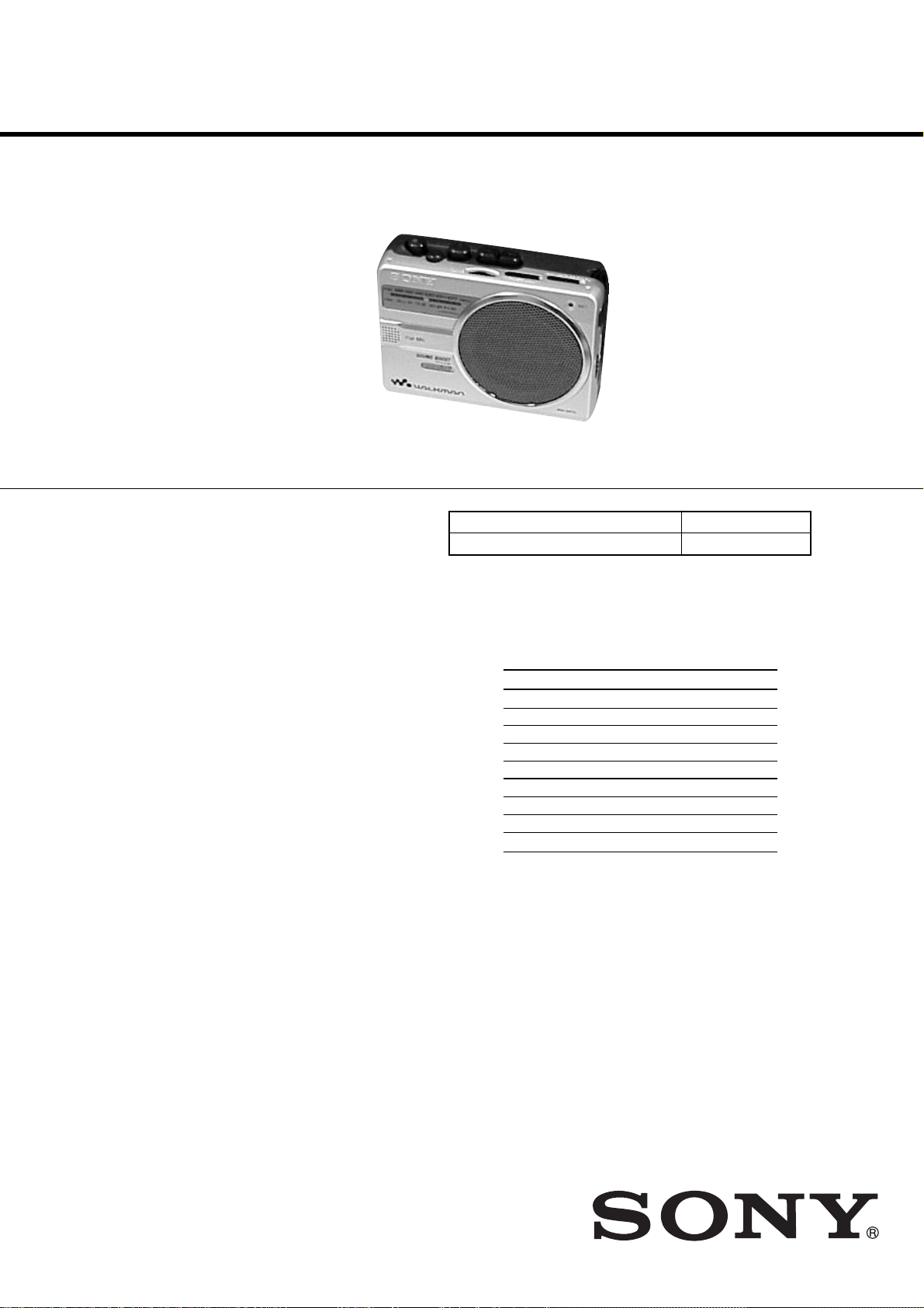
WM-SR10
SERVICE MANUAL
Ver 1.1 2003. 05
Model Name Using Similar Mechanism WM-GX221
Tape Transport Mechanism Type MT-WMGX221-175
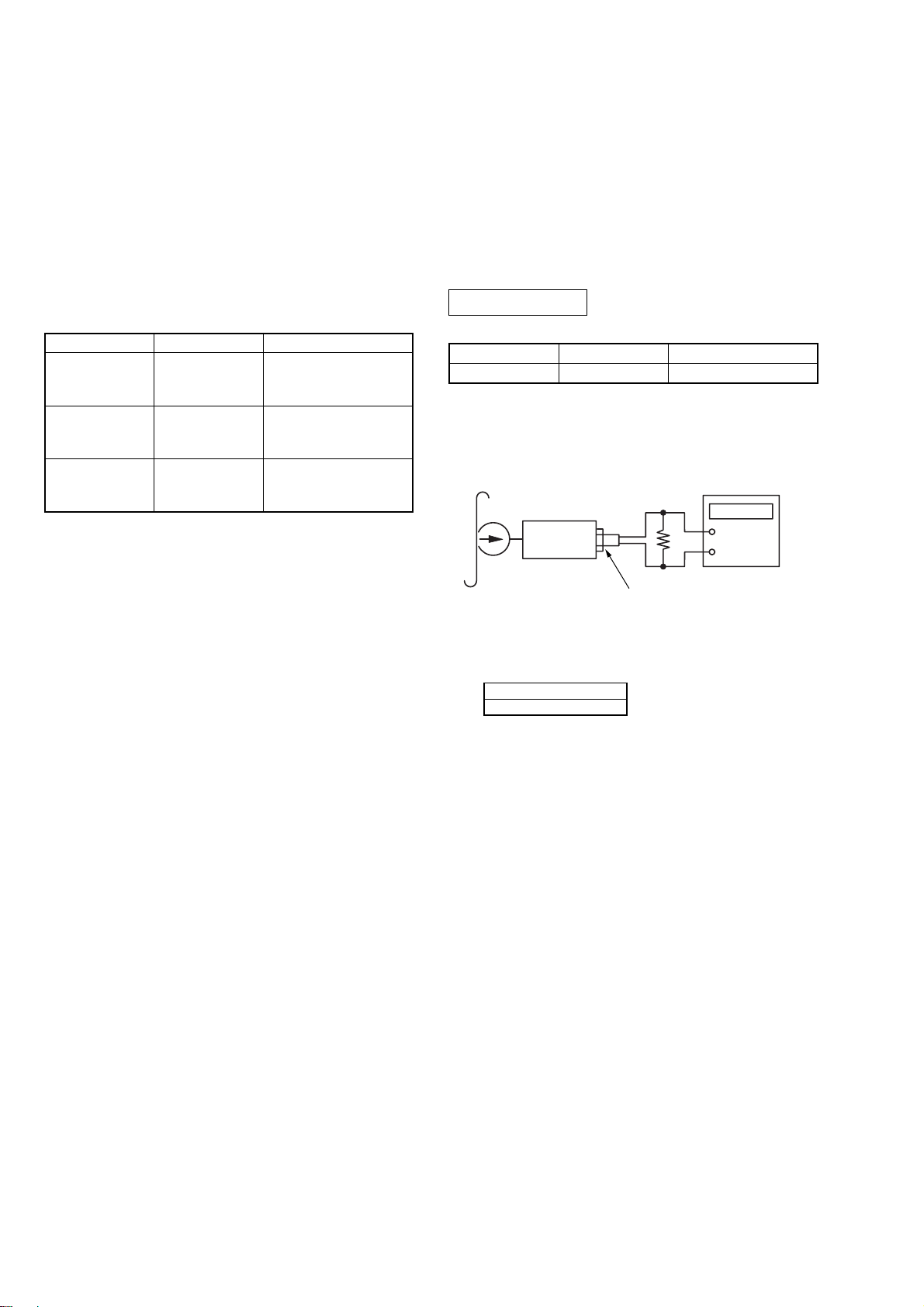
SPECIFICATIONS
E Model
Frequency range
FM: 87.5 - 108 MHz (Saudi Arabia)
87.6 - 107.9 MHz (Other countries)
AM: 526.5 - 1 606.5 kHz (Saudi Arabia)
531 - 1 602 kHz (Other countries)
Frequency response Playback: 40 - 15 000 Hz
Input Microphone (MIC) jack
Output Headphones (i) jack, Load impedance 8 - 300 Ω
Speaker
Power requirement 3V DC
Dimensions
Approx. 112.0 × 82.5 × 37.5 mm (4
(w/h/d), excl. projecting parts and controls
Mass Approx. 187 g (6.6 oz) (main unit only)
Supplied accessory
Stereo headphones or Stereo earphones (1)
Design and specifications are subject to change without
notice.
Recording: 100 - 8 000 Hz
Approx. 5 cm (2 in.) dia.
Batteries R6 (AA) x 2
External DC 3 V power sources
1
⁄2 × 3 1⁄4 × 1 1⁄2 inches)
Battery life* (approximate hours)
Sony alkaline LR6(SG)**Sony R6P(SR)
(using headphones/earphones)
Tape playback 24 7
Radio reception 48 15
Mic recording 20 4.5
Radio recording 12 3
(using the speaker)
Tape playback 15 4.5
Radio reception 26 6
Radio recording 11.5 3
* Measured value by the standard of JEITA (Japan Electronics and
Information Technology Industries Association).
(Using a Sony HF series cassette tape)
** When using LR6 (SG) Sony “STAMINA” alkaline dry batteries
(produced in Japan).
Note
The battery life may be shorter depending on the operating
condition, the surrounding temperature and battery type.
9-874-215-02
2003E16-1
© 2003.05
RADIO CASSETTE-CORDER
Sony Corporation
Personal Audio Company
Published by Sony Engineering Corporation
Page 2

WM-SR10
TABLE OF CONTENTS
1. SERVICE NOTE ............................................................... 3
2. GENERAL .......................................................................... 4
3. DISASSEMBLY
3-1. Front Cabinet Assy.......................................................... 5
3-2. MAIN Board ................................................................... 6
3-3. Mechanism Deck (MT-WMGX221-175) ....................... 6
3-4. Belt (CAP), M601, HRP901, HE901 .............................. 7
3-5. Cassette Holder Sub Assy ...............................................7
4. MECHANICAL ADJUSTMENT .................................. 8
5. ELECTRICAL ADJUSTMENT .................................... 8
6. DIAGRAMS ...................................................................... 10
6-1. Block Diagram – Tuner Section –................................. 11
6-2. Block Diagram – Main Section – ................................. 12
6-3. Printed Wiring Boards .................................................. 13
6-4. Schematic Diagram – MAIN Board (1/2) –.................. 14
6-5. Schematic Diagram – MAIN Board (2/2) –.................. 15
6-6. IC Block Diagrams ....................................................... 16
7. EXPLODED VIEWS
7-1. Overall Section ............................................................. 17
7-2. Cabinet (Front) Section ................................................. 18
7-3. Mechanism Deck Section-1 (MT-WMGX221-175) ..... 19
7-4. Mechanism Deck Section-2 (MT-WMGX221-175) ..... 20
8. ELECTRICAL PARTS LIST .......................................21
Notes on chip component replacement
•Never reuse a disconnected chip component.
• Notice that the minus side of a tantalum capacitor may be
damaged by heat.
Flexible Circuit Board Repairing
•Keep the temperature of soldering iron around 270˚C
during repairing.
• Do not touch the soldering iron on the same conductor of the
circuit board (within 3 times).
• Be careful not to apply force on the conductor when soldering
or unsoldering.
Unleaded solder
Boards requiring use of unleaded solder are printed with the leadfree mark (LF) indicating the solder contains no lead.
(Caution: Some printed circuit boards may not come printed with
the lead free mark due to their particular size.)
: LEAD FREE MARK
Unleaded solder has the following characteristics.
• Unleaded solder melts at a temperature about 40°C higher than
ordinary solder.
Ordinary soldering irons can be used but the iron tip has to be
applied to the solder joint for a slightly longer time.
Soldering irons using a temperature regulator should be set to
about 350°C.
Caution: The printed pattern (copper foil) may peel away if the
heated tip is applied for too long, so be careful!
• Strong viscosity
Unleaded solder is more viscous (sticky, less prone to flow) than
ordinary solder so use caution not to let solder bridges occur such
as on IC pins, etc.
• Usable with ordinary solder
It is best to use only unleaded solder but unleaded solder may
also be added to ordinary solder.
2
Page 3
SECTION 1
SERVICE NOTE
In this set, record/play mode is detected using the switch S704 (TAPE POWER).
S704 is mounted on the MAIN board. If MAIN board is removed, it becomes impossible to detect
record/play mode.
Where MAIN board is removed, when you measure operation and voltage of each part of the mechanism
deck, please turn on S704.
– MAIN Board (SIDE A) —
WM-SR10
S704
3
Page 4
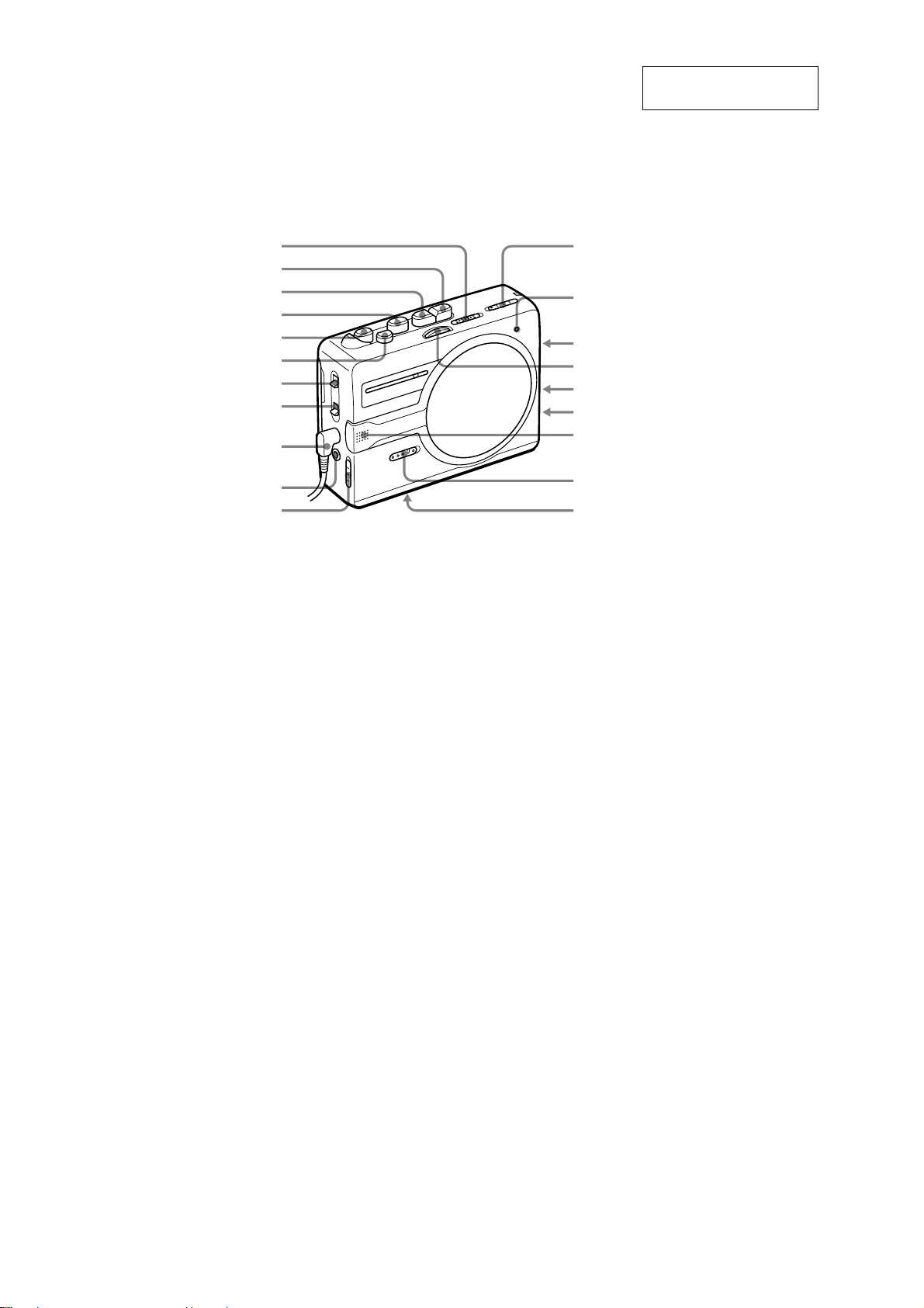
WM-SR10
• LOCATION OF CONTROLS
SECTION 2
GENERAL
This section is extracted
from instruction manual.
PAUSE
MFF/CUE
mREW/REVIEW
NPLAY**
zREC
xSTOP
ISS
FM ST/MONO
i
MIC (PLUG IN POWER)**
AVLS
* There is a tactile dot beside VOL on the main unit to show the direction to turn up the volume.
** The button/jack has a tactile dot.
(RADIO OFF) TAPE/
AM/FM
BATT indicator
VOL*
TUNING
SPEAKER/ i
DC IN 3 V
Built-in microphone
SOUND BOOST
Battery compartment
4
Page 5
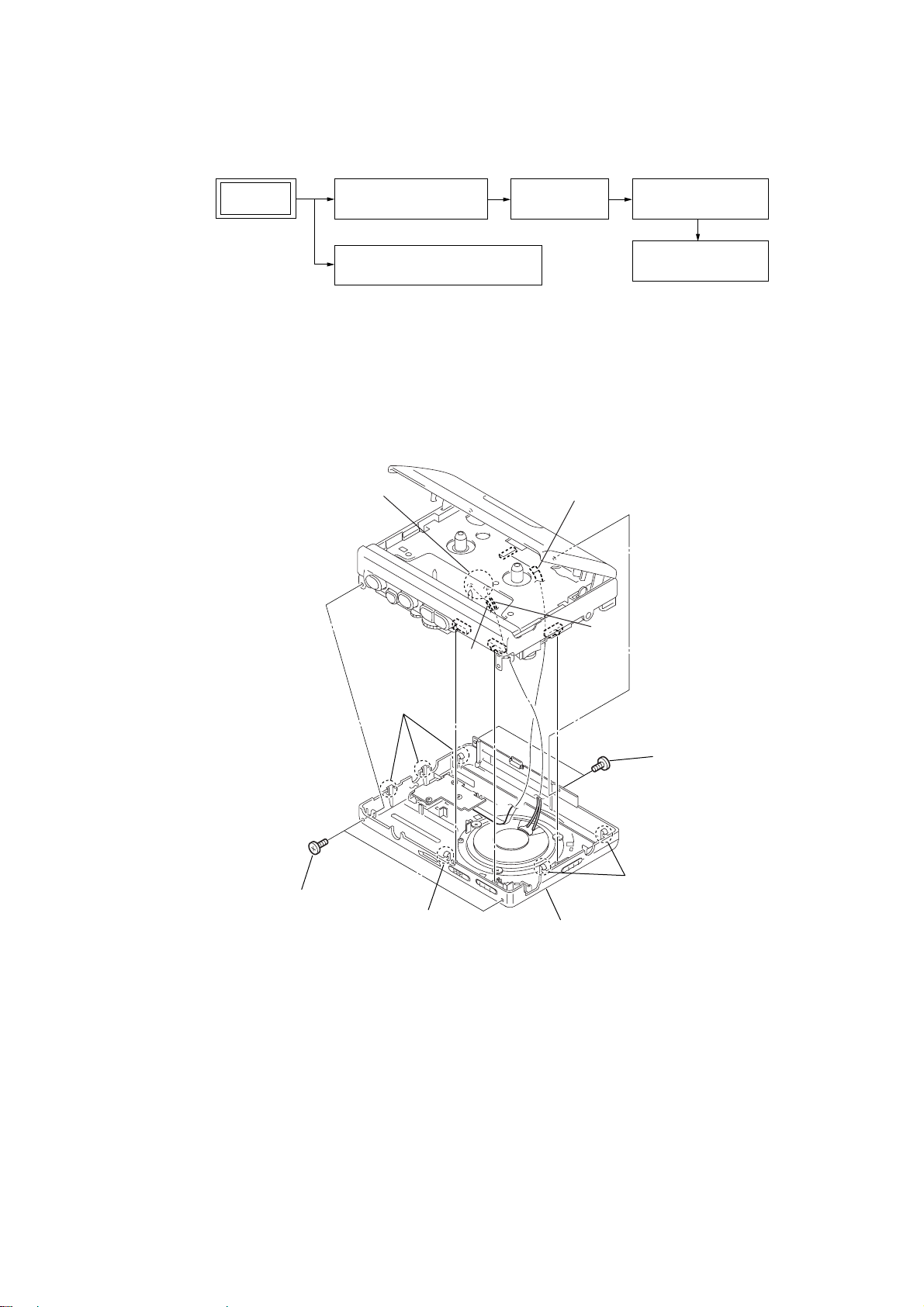
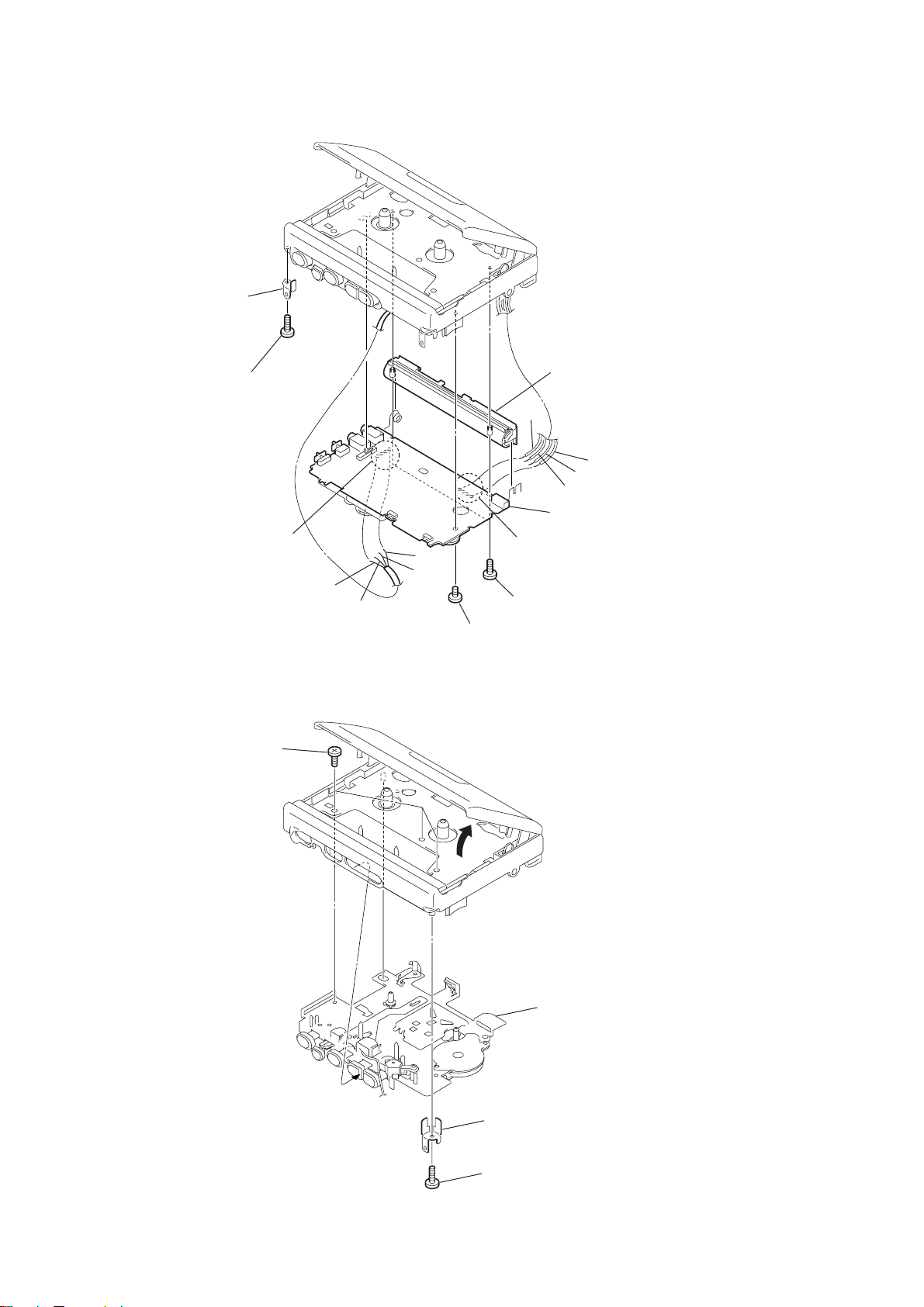
Note : Disassemble the unit in the order as shown below.
WM-SR10
SECTION 3
DISASSEMBLY
SET
FRONT CABINET ASSY MAIN BOARD
CASSETTE HOLDER SUB ASSY
Note : Follow the disassembly procedure in the numerical order given.
3-1. Front Cabinet Assy
7
Remove soldering
from the two points.
6
flexible flat cable
(CN701)
RED
MECHANISM DECK
(MT-WMGX221-175)
BELT (CAP), M601,
HRP901, HE901
2
two screws
(M1.4) (EG)
3
three claws
4
claw
WHT
8
front cabinet assy
1
5
two claws
two screws
(TP 1.7
×
3.7)
5
Page 6
WM-SR10
3-2. MAIN Board
2
plate connector (L)
1
screw
(TP B1.7
3
Remove soldering
from the four points.
×
4)
RED
BLU
GND
WHT
5
8
ORG
BLK
7
4
Remove soldering
from the four points.
6
two screws
(TP B1.7
screw
×
3)
(M1.4
joint cover
RED
WHT
MAIN board
×
4)
3-3. Mechanism Deck (MT-WMGX221-175)
2
three screws
(IB LOCK)
1
4
plate connector (R)
5
mechanism deck
(MT-WMGX221-175)
3
screw
(TP B1.7 × 4)
6
Page 7
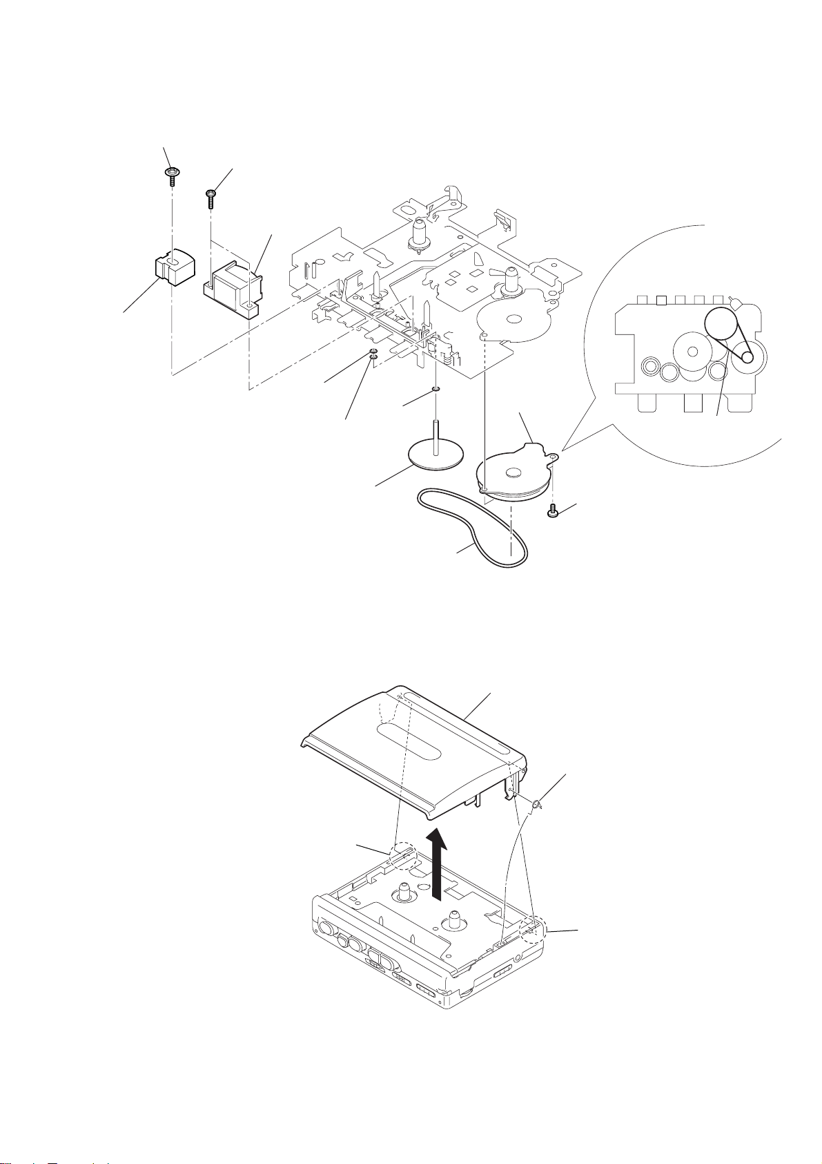
3-4. Belt (CAP), M601, HRP901, HE901
)
screw
0
8
two screws
9
HRP901
(REC/PB head)
HE901
qa
(erase head)
4
washer
(stopper N)
5
washer
7
washer
M601
3
(capstan/reel
motor)
WM-SR10
z
Attaching belt (CAP).
belt (CAP)
capstan fly assy (AR)
6
3-5. Cassette Holder Sub Assy
2
boss
1
belt (CAP)
3
two screws (M1.4)
2
5
cassette holder sub assy
4
spring (torsion
1
boss
7
Page 8
WM-SR10
r
SECTION 4
MECHANICAL ADJUSTMENT
SECTION 5
ELECTRICAL ADJUSTMENT
PRECAUTION
1. Clean the following parts with a denatured-alcohol-moistened
swab:
record/playback/erase head pinch roller
rubber belts capstan
2. Demagnetize the record/playback head with a head demagnetizer. (Do not bring a head demagnetizer close to the erase
head.)
3. Do not use a magnetized screwdriver for the adjustments.
4. The adjustments should be performed with the rated power
supply voltage unless otherwise noted.
• Torque Measurement
Mode
FWD
FWD
Back Tension
FF, REW
Torque Meter
CQ-102D
CQ-102D
CQ-201B
Meter Reading
19.6 to 39.2 mN•m
(20 to 40 g•cm)
(0.28 to 0.56 oz•inch)
0.49 to 4.9 mN•m
(0.5 to 5.0g•cm)
(0.0069 to 0.069 oz•inch)
More than 49 mN•m
(More than 50 g•cm)
(More than 0.69 oz•inch)
PRECAUTION
1. Specified voltage: 2.5 V (DC)
2. Switch and control position
VOL : MAX
SPEAKER : OFF
AVLS : NORM
SOUND BOOST : OFF
PAUSE : OFF
ISS : 1
FM MODE : FM ST
TAPE SECTION
Set
Signal
3 kHz, 0 dB
2
jack (J301)
16
Ω
Tape
WS-48A
Tape Speed Adjustment
Procedure:
Test tape
WS-48A
(3kHz, 0dB)
1. Enter the FWD playback mode.
2. Adjust RV601 so that the value of the frequency counter reading
becomes 3,000 Hz.
Specification value:
Frequency counter
2,985 Hz – 3,015 Hz
3. Check that the frequency deviation at the beginning and ending
of a tape is within 1.5 % (45 Hz).
Used for
Ta pe Speed Adjustment
+
–
Frequency counte
Adjustment Location : MAIN Board (see page 9)
8
Page 9

WM-SR10
r
TUNER SECTION
0dB=1µV
[AM]
BAND : AM
AM RF signal
generator
30% amplitude modulation by 400 Hz
signal.
Output level : as low as possible
Put the lead-wire
antenna close to
the set.
[FM]
BAND : FM
FM RF signal
generator
0.01µF
75kHz frequency deviation by 1kHz signal.
Output level : as low as possible
to ANT (FM IN)
•Repeat the procedures in each adjustment several times.
AM FREQUENCY COVERAGE ADJUSTMENT
Adjust for a maximum reading on level meter.
L4 505 kHz (516.5 kHz)
CT1-4 1,680 kHz (1,631.5 kHz)
( ) : EA MODEL
AM TRACKING ADJUSTMENT
Adjust for a maximum reading on level meter.
L1 621 kHz
CT1-1 1,404 kHz
AM IF ADJUSTMENT
Adjust for a maximum reading on level meter.
T1 455 kHz
FM FREQUENCY COVERAGE ADJUSTMENT
Adjust for a maximum reading on level meter.
L3 86.0 MHz (87.35 MHz)
CT1-3 109.5 MHz (108.25 MHz)
( ) : EA MODEL
set
2
jack (J301)
Adjustment Parts Location :
[MAIN Board] — SIDE A —
CT1-3 : FM frequency
coverage adjustment
CT1-3
CT1-2
Ω
16
+
–
level mete
CT1-4 : AM frequency
CT1-4
CT1-1
coverage adjustment
FM TRACKING ADJUSTMENT
Adjust for a maximum reading on level meter.
L2 86.0 MHz (87.35 MHz)
CT1-2 109.5 MHz (108.25 MHz)
•Abbreviation
EA : Saudi Arabia model
[MAIN Board] — SIDE B —
RV601 : Tape speed adjustment
L4 : AM frequency
coverage adjustment
L3 : FM frequency
coverage adjustment
RV601
L1
L4
( ) : EA MODEL
T1 : AM IF
adjustment
T1
L3
L2
CT1-2 : FM tracking
adjustment
CT1-1 : AM tracking
adjustment
L1 : AM tracking
adjustment
L2 : FM tracking
adjustment
9
Page 10

WM-SR10
SECTION 6
DIAGRAMS
Note on Schematic Diagram:
• All capacitors are in µF unless otherwise noted. p: pF.
50 WV or less are not indicated except for electrolytics and
tantalums.
• All resistors are in Ω and 1/
• C : panel designation.
• A : B+ Line.
• H : adjustment for repair.
•Total current is measured with no cassette installed.
•Power voltage is dc 3 V and fed with regulated dc power supply
from external power voltage jack (J401).
•Voltages and waveforms are dc with respect to ground under nosignal (detuned) conditions.
no mark : FM
(): PB
•Voltages are taken with a VOM (Input impedance 10 MΩ).
Voltage variations may be noted due to normal production tolerances.
•Waveforms are taken with a oscilloscope.
Voltage variations may be noted due to normal production tolerances.
• Circled numbers refer to waveforms.
• Signal path.
F : FM
f : AM
E : PB
d : REC
N : MIC INPUT
•Abbreviation
9E : E model without the indication of the country of origin.
EA : Saudi Arabia model
4
W or less unless otherwise specified.
Note on Printed Wiring Board:
• Y : parts extracted from the conductor side.
a
•
Caution:
Pattern face side: Parts on the pattern face side seen from
(Side B) the pattern face are indicated.
Par ts face side: Parts on the parts face side seen from
(Side A) the parts face are indicated.
: Through hole.
• WAVEFORMS
1
T551 (REC mode)
21
µ
10 V/DIV, 10 µs/DIV 1 V/DIV,
s
42 Vp-p
2
IC301 r; (VOUT)
(PB mode)
4.4 ms
2 ms
/DIV
2.7 Vp-p
10
Page 11

6-1. Block Diagram – Tuner Section –
WM-SR10
• SIGNAL PATH
: FM
X2
10.7MHz
12
QUAD
FM
DET
LEVEL
DET
AM
DET
AGC
FM
MUTE
TUN
LED
TUN LED
BUFFER
ST
LED
ST LED
11
AF
AMP
LP1
MO-ST
151610
MPX-IN
DIVIDER/
VCO
DECODER
AMP
SWITCH
S1
FM ST MONO
DET-OUT
AF
18 17
PD1
PD2
LP2
BAND
L OUT
R OUT
14
13
FM
RF AMP
AM
RF AMP
IC1
FM-RF OUT
CT1-3, L3
FM FREQUENCY
COVERAGE
FM/AM
MIX AMP
FM/AM
OSC
FM OSC
AM OSC
2123
20
MIX
CT1-4, L4
AM FREQUENCY
COVERAGE
CF2
4 8
AM IF
10.7MHz
T1
CF1
455kHz
FM
IF IN
FM
IF AMP
AM
IF IN
7
AM
IF AMP
FM/AM RF AMP, FM/AM MIX AMP,
FM/AM OSC, FM/AM IF AMP, DET, MPX
ANT
A
C2
L1
AM
FERRITE BAR
ANTENNA
CT1-1, L1
AM TRACKING
CP1
B.P.F.
CT1-1 CV1-1
L2
FM RF
CT1-2, L2
FM TRACKING
FM-RF
IN
1
AM-RF
IN
24
CT1-2 CV1-2
: AM
TU L, TU R
B
L3
FM OSC
CV1
TUNING
CT1-3 CV1-3
L4
AM OSC
Q33, 34
CT1-4CV1-4
AM
D
FM
E
D33
BAND SELECT
SWITCH
Q30, 32
MUTING
CONTROL
TUNER MUTING
JR3
C
R5
TU VCC
1111
Page 12

WM-SR10
6-2. Block Diagram – Main Section –
TU L, TU R
B
J501
(PLUG IN POWER)
MIC
MIC501
FLAT MIC
TUNER MUTING
C
21
19
MIC
IN (L)
MIC
IN (R)
IC501 (1/2)
MIC AMP, ALC
ALC
ALC
MIC
AMP
MIC
AMP
MIC
OUT (L)
MIC
OUT (R)
TU L TU R
16
17
IC501 (2/2)
REC/PB AMP
BUF
IN (L)
Q706
14
BUF
IN (R)
13
+
+
MUTING
MODE
CONTROL
CIRCUIT
PB AMP
REC AMP
PB AMP
REC AMP
OUT (L)
REC
OUT (L)
OUT (R)
REC
OUT (R)
LINE SW
REC SW
PW SW
PB
8
2
PB
9
3
15
11
12
TU B+
PB/REC
REC VCC
MAIN VCC
S304
AVLS
NORM
LIMIT
Q252
PRE AMP
4
3
2
BYPASS
IC151
POWER AMP
–
+
SHUT DOWN
1
–
+
5
8
Q717,718
CONTROL
Q714
MUTING
+
MUTING
D234
SP251
(SPEAKER)
HRP901
(REC/PB)
L-CH
R-CH
HE901
(ERASE)
BATT B+
M601
(CAPSTAN/REEL)
S301 (3/4)
(REC/PB)
REC PB
MAIN VCC
COM
WV
Q551
ISS
SWITCH
U
S301 (1/4)
(REC/PB)
REC PB
S301 (2/4)
(REC/PB)
REC PB
VREF
T551
BIAS OSC
3
S551
2
ISS
1
PRE AMP, POWER AMP, MEGA-BASS
FWDIN (L)
9
10
REVIN (L)
FWDIN (R)
11
12
REVIN (R)
VREF
13
Q553
REC
BIAS OSC
OUT
37
UOUT
39
VOUT
40
WOUT
41
IC301 (1/2)
EQ
AMP
EQ
AMP
MAIN VCC
PB/REC
COMPARATOR
CONTROL
MOTOR
CIRCUIT
MUTING
PRE-OUT (L)
PRE-NF (L)
PRE-NF (R)
PRE-OUT (R)
S301 (4/4)
(REC/PB)
REC PB
+
VSP
–
SPEED
DRIVE
IN+
5
6
8
7
35
36
SWITCH &
LOGIC
CIRCUIT
EQ
EQ
OSC
CIRCUIT
OSC
47
TH601
+
S303
SOUND BOOST
OFF
ON
34
M-VREF
BIAS
REFERENCE
VOLTAGE
IC301 (2/2)
CAPSTAN/REEL
MOTOR DRIVE
+
LOW
BOOST
L.B-SW
32
TAPE SPEED
RV601
S/S
3
30
MIX-IN (R)
29
MAIN VCC
MIX-IN (L)
Q702
MIX 1
+
–
MIX 2
–
+
–
+
VREF
POWER MUTE
SWITCH
Q703, 711
START/STOP
CONTROL SWITCH
PB/REC PAUSE
NF
Q707
DET
MIX-OUT (L)
MIX-OUT (R)
POWER
MUTE
21
S702
PAUSE
L
R
CONTROL
24
25
SYSTEM
15
D35
D32
PB/REC
MAIN VCC
OFF
ON
Q302
AVLS
SWITCH
Q704
PRE MUTE
SWITCH
H/P MUTE
MUTING
MAIN VCC
PB/REC
MAIN VCC
Q705
H/P MUTE
SWITCH
D701
Q722
MUTING
CONTROL
Q720
MUTING
CONTROL
Q31, 709
MUTING
CONTROL
Q719
MUTING
CONTROL
RV301
VOL
PB/REC
TU B+
MAIN VCC
H/P MUTE
22
SPEAKER
POWER
IN (L)
S701 (2/2)S701 (1/2)
i
POWER
AMP
BATT B+
POWER
OUT (L)
Q710
SWITCH
16
TU B+
PB/REC
(HEADPHONE)
J301
MUTING
i
+
AMP
AMP
POWER
OUT (R)
20
POWER
OUT (COM)
18
Q401, 403
RIPPLE
FILTER
Q402
SWITCH
D302
D401
BATT
D301
BATT B+
S703
(FUNCTION)
FM
AM
TAPE
(RADIO OFF)
ANT
A
• SIGNAL PATH
: TUNER (FM/AM)
: TAPE PLAY
: TAPE REC
: MIC INPUT
DRY BATTERY
SIZE ‘‘AA’’
(IEC DESIGNATION R6)
2PCS. 3V
–
J401
DC IN 3V
+
MUTING
TU VCC
REC VCC
PB/REC
MIC B+
REC VCC
MAIN VCC
TU B+
(ON at FF/REW/PLAY modes.)
POWER
IN (R)
23
VREF
S704
(TAPE POWER)
POWER
POWER
Q712, 713
B+ SWITCH
Q701,715
B+ SWITCH
Q501, 502
B+ SWITCH
AM
D
FM
E
1212
Page 13

WM-SR10
6-3. Printed Wiring Boards
A
B
IC301
C
• : Uses unleaded solder.
S703
TAPE
(RADIO OFF)
SP251
(SPEAKER)
BATT
IC151
WHT
–1 –2
RED
RED
WHT
BLK
ORG
/REEL MOTOR
COM
W
V
U
WHT
BLK
D
E
F
G
IC1
(ERASE)
• Semiconductor Location
CV1
TUNING
IC501
Ref. No. Location
D32 B-8
D33 D-3
D34 A-4
D35 A-8
D234 C-8
D301 A-4
RED
BLU
WHT
BLK
D302 D-8
D401 A-6
D701 D-1
CF2
IC1 F-3
IC151 B-7
CF1
X2
IC301 C-2
IC501 E-9
Q30 D-2
Q31 C-3
Q32 C-3
Q33 C-3
Q34 D-3
Q252 B-7
Q302 B-3
MONO
S1
FM ST
Q401 A-1
Q402 A-2
Ref. No. Location
Q403 A-1
Q501 E-1
Q502 E-1
Q551 F-1
Q553 E-1
Q701 D-1
Q702 C-6
Q703 C-1
Q704 D-1
Q705 B-2
Q706 E-9
Q707 B-8
Q709 C-8
Q710 D-1
Q711 C-1
Q712 D-8
Q713 D-8
Q714 C-7
Q715 D-1
Q717 C-7
Q718 C-7
Q719 D-8
Q720 C-8
Q722 D-8
12
3456789101112 13
1313
Page 14

WM-SR10
6-4. Schematic Diagram – MAIN Board (1/2) –
Q501
C503
0.1 B
C502
0.1 B
UN5114-TX
Q502
XP1214
47
R505
C504
2.2k
R504
2.2k
C505
0.01 B
4V (A)
10V (B)
22
1M
R507
C508
TA8155FN(ER)
F
1
47
C510
C509
2.2k
2.2k
R508
R509
C514
1F
47k
R506
B
0.01
C507
IC501
1k
R503
10V (B)
2.2k
R501
2.2k
R502
L
MIC
R
MIC
FB501
FB
1K
FB502
FB 1K
FB503
J501
FB 1K
MIC
MONO
• Refer to page 16 for IC Block Diagram.
B
B
F
C515
C513
1
C512
2200p
2200p
10k
R510
220k
R511
C516
4V (A)
B
C511
22
470p
10k
C521
R516
REC
VCC
R716
10k
C519
R515
10k
0.1 F
R514
10k
C520
0.47 F
F
C517
0.1
F
0.47
C518
R512
220k
R513
10k
1F
Q701
XP1215
R717
F
2.2
C522
0
2SB1679
Q706
XP1215
0
0
J10
J9
F
F
0.47
0.47
C28
C27
B
47k
470p
R517
C523
Q715
S1
CH
UJ
4
C3
1000p
B
C32
1000p
B
C40
1000p
SL
FB2
1K FB
CP1
TP3
FM
FM BPF
IN
C2
1000p
BP1
C33
2200p
SL
-1
1p
C7
TP8
AM RF
J7 C14
0 4.7
C38
100p
10p
L1
SL
R465
AM ANT
R459
470
2.2k
CT1
SML-210LT-T86
L2
CV1
C9
TP1
TU
GND
D401
-2
-2
FM RF
CV1
CT1
C10
AM IFT
C11
0.47 B
C37
100p SL
MA111
D301
D302
1
-1
3
2
L3
FM OSC
C12
R3
0
T1
MA111
S703
-3
-3
CN701
6 PIN
L4
CV1
CT1
AM OSC
C5
6p
IC1
TA2111FN(EL)
B
SL
C17
C39
0.047
1000p
C15
C13
470
4V (A)
R2
1k
R9
5
-4
-4
CV1
C18
CT1
C30
0.22
CF1
455kHz BPF
CF2
10.7MHz BPF
CN702
6PIN
C560
0.1 B
F
MONO STEREO
1000p
B
C501
0.22
S304
0
10k
R5
JR3
TP6
MIC501
F
47k
100k
25V
R6
R10
0.1
C23
TP2
TU
VCC
D34
MA111
1
F
10.7MHz
C29C22
0.1
16V
F
X2
C26
UN5214-TX
10V (B)
47
C24
4700p
Q33
C25
4700p
TP5
TU
TP4
R
TU
L
100k
100k
R7
R8
Q712
R719
2SB1679
47k
R718
10k
Q713
2SA1162-YG-TE85L
R34
1k
2.2k
R31
Q34
DTC114YUA
R30
100k
0
C35
2F
FB1
10
R11
R724
1M
C707
C34
R32
2F
1M
R33
100k
Q32
MA111
2SA1162-YG
-TE85L
D33
Q30
DTA114TUA
R64
1M
220
R713
22k0.01 B
Q720
DTA114TUA
R725
2F
R257C250
100k
C251
C153
0.1 F
R250
D234
R258
Q710
XP4215-TX
R259C252 100k0.022 B
4V EC
0
S701(2/2)
IC151
LM4871MM
MA111
SP-MUTE
220k
C253
0.47
R711
R712
10k
10k
R706
220k
R255
470k
Q714
UN5215-TX
R252
470k
Q717, 718
Q718
DTA115TUA
B
C210
0.1
Q717
DTA114TUA
R708
1M
C705
B
R707
220k
2F
C710
2F
R254
22k
SP251
10k
R256
C21
50V
B
TP7
DET
OUT
S303
1414
Page 15

WM-SR10
6-5. Schematic Diagram – MAIN Board (2/2) –
C103
470p B
C101
S301(3/4)
C316
1000p B
C506
1F
R551
S551
47
C551
Q551
XP1501
CH
C552
470p
B
0.01
1k
R552
47k
R553
• Refer to page 10 for Waveforms. • Refer to page 16 for IC Block Diagrams.
C203
470p B
B
10k
B
10k
C102
2200p
R101
S301(1/4) S301(2/4)
F
1
B
470p
C104
CH
C553
220p
B
47k
C554
0.01
R554
C202
R201
2200p
F
1
C201
PB
REC
B
C205
4700p
R206
R213
2.2k
B
C301
1000p
B
470p
C204
T551
BIAS-OSC
B
C555
2200p
1k
R555
R560 100
47
R556
R557
2SD596-T1DV4
4.7k
R559
10k
C557
0.022 B
C556
10V (B)
47
F
F
1
1
C207
C107
R204 R104
10k 10k
1k
4V (A)
C206
22
Q553
C558
BIAS OFF
4700p
R103R203
22k22k
R105R205
R212
2.2M
B
R558
10
1M1M
R112
2.2M
S301(4/4)
R722
1M
R723
100k
Q722
DTA114TUA
C709
12F
Q703
XP1215
1k
R605
R601
22k
D701
DAN202U
PAUSE
R603
47k
C601
0.01 B
Q704
XP4315
EC
4V
C319
Q711
UN5116
B
C105
4700p
1k
R106
R113
2.2k
4V (A)
C106
22
220
R703
REF
Q702
UN5214-TX
R602
4.7k
V
MIX-IN
R
MIX-IN
L
R610
MAIN
0
R115
0
R607
10k
3900PPM
3.3K
0
R303
10k
1000p B
1F
1F
2SA1162-YG
Q252
RV601
0.1 B
4.7k
0.022
22k
C307
V
REF
B
R215
BOOST
Q705
UN5215-TX
RV301
10k/10k
C263
0.22 16V B
C318
10 10V
R315
100k
0.1 B
S701(1/2)
C303
100p
CH
R302
100k
C317
22
6.3V
C304
2.2 F
C305
1F
H/P
MUTE
R304
1k
C315
1k
R263
Q719
DTA114TUA
C706
R702
100k
AVLS
S702
MA111
D32
MA111
D35
C703
F
C701
0.01
10k
R264
Q707
UN5214-TX
10K/47K
C264
0.01 F
B
0.01
B
B
B
B
0.1
0.1
0.1
0.22
C603
C605
C604
C602
IC301
LB8115W-NA-TLM
2.2
R305
F
1
C308
B
F
F
0.1
0.1
10V (B)
1000p
22
C311
C309
C312
C310
10V (B)
22
C313
B
0.22
C607
C606
2.2 B
R604
100k
TH601
R606
1k
R608
R613
C108
1000p B
C208
C306
Q302
XP4501-TX
R207
100
R107
100
C109
R208
2.2k
2.2k
R108
R260
100k
B
B
B
0.47
SL
1000p
1000p
C314
100p
C211
C111
C405
C209
1k
R160
100k
R265
B
C400
0.1
470k
2.2k
R261
R262
VCC
4V
C404
220
Q31
DTA114TUA
R710
1M
2F
R62
C36
1M
2F
R63
100k
Q403
2SB1679
10k
4.7k
R402
Q401
XP1501
1k
R401
XP1214
C401
Q402
R705
1M
Q709
XP4315
R210
1k
R405
2.2k
R403
B
1000p
R704
R110
470k
220k
C402
10V (B)
R406
R404
22
1M
C708
2F
1k
HP/R
10
R209
10
R109
HP/L
0
R309
HP/COM
TAPE-SW
1
R609
1
+B
4V
C403
220
GND
FB201
FB 1K
FB101
FB 1K
FB301
FB 1K
S704
J401
M601
J301
1515
Page 16

WM-SR10
6-6. IC Block Diagrams
AM-RF IN
23
24
FM
RF
VCC1
FM-RF OUT
21
22
FM OSC
FM MIX
1
FM-RF IN
FM OSC
2
GND
AM OSC
AM MIX
3 4
LPF3
AM OSC
20
MIX
IC1 TA2111FN (EL)
DET-OUT
AFC
1819
FM
IF
FM
MUTE
AM DET
FM DET
FM
AM
AGC
5
6 7
AGC
VCC2
IF
AM IF IN
IF
8
FM IF IN
LEVEL
DET
9
17
AF
GND2
MPX-IN
16
DIVIDE
TUNE
LP1 MO-ST
L OUT
LP2 BAND
VCO
LED
10 11 12
TUN-LED
13
1415
DECODE
ST
LED
ST-IND
R OUT
ST/MO
FM/AM
QUAD
SHUTDOWN
BYPASS
+IN
IC151 LM4871MM
VO2
1
2
3
-IN
4
BIAS
VDD/2
AV=-1
8
GND
7
VDD
6
VO1
5
COM
PRE-GND
PRE-OUT (L)
PRE-NF (L)
PRE-OUT (R)
PRE-NF (R)
FWDIN (L)
REVIN (L)
FWDIN (R)
REVIN (R)
S/S
IC301 LB8115W-NA-TLM IC501 TA8155FN (ER)
M-VCC
OSCUBVB
48 47 46 45 44 43 42 41 40 39 38 37
1
REF
VOLTAGE
2
RI
BIAS
3
4
5
6
7
8
9
10
11
12
REF
OSC
CURRENT
DET
WB
FWD/
REV
OPERATION
DET
SYS
CONT
DR
MPGND
WOUT
VOUT
PRE DRIVER
OPERATION LOGIC
PULSE DET
REF VOLTAGE
FOR SPEED CONTROL
DET
–
+
UOUT
SPEED
FC
FREQ
CARC.
OUT
LOW
BOOST
36
VSP
35
IN
34
M-VREF
33
M-GND
32
L. B-SW
31
DET-OUT
30
MIX-IN (L)
29
MIX-IN (R)
28
H.PIN (L)
27
H.PIN (R)
26
LP.2
25
MIX-OUT (R)
ALC
DET
ALC
ALC
RADIO / TAPE
24
23
22
21
20
19
18
17
16
15
14
ALC
VCC
MIC NF (L)
MIC IN (L)
GND
MIC IN (R)
MIC NF (R)
MIC OUT (R)
MIC OUT (L)
LINE SW
BUF IN (L)
VREF
1
2
3
4
5
6
7
8
9
10
11
REC AMP
VREF
PB AMP
PB AMP
REC / PB
VCC (REC)
REC OUT (L)
REC OUT (R)
PB IN (L)
+
PB IN (R)
PB NF (L)
PB OUT (L)
PB OUT (R)
PB NF (R)
REC SW
R.F
13 14 15
VREF
R.P-REF
16
17
(L)
SYSTEM
POWER-OUT
VREF
18 19 20 21 22 23 24
(R)
VCC
(COM)
POWER-GND
POWER-OUT
POWER-MUTE
POWER-OUT
(L)
POWER-IN
(L)
(R)
MIX-OUT
POWER-IN
PW SW
12
PW SW
13
BUF IN (R)
1616
Page 17

NOTE:
• -XX, -X mean standardized parts, so they may
have some differences from the original one.
• Items marked “*” are not stocked since they
are seldom required for routine service. Some
delay should be anticipated when ordering these
items.
7-1. Overall Section
SECTION 7
EXPLODED VIEWS
• The mechanical parts with no reference number
in the exploded views are not supplied.
• Accessories are given in the last of this parts
list.
23
WM-SR10
•Abbreviation
9E : E model without the indication of the
country of origin.
EA : Saudi Arabia model
19
21
20
18
a
7
MT-WMGX221-175
15
14
13
12
11
17
10
16
7
19
* 9
22
27
25
28
a
3
cabinet (front) section
L1
2
1
8
#1
26
7
6
5
4
Ref. No. Part No. Description Remarks Ref. No. Part No. Description Remarks
1 3-244-967-01 KNOB (TUNING)
2 3-237-136-01 GEAR (B)
3 3-225-996-11 SCREW (M1.4)(EG),PRECISION PAN
4 3-244-968-01 POINTER
5 3-244-969-01 HOLDER (GEAR)
6 3-345-648-95 SCREW (M1.4), TOOTHED LOCK
7 3-318-203-61 SCREW (B1.7X4), TAPPING
8 3-237-135-01 GEAR (A)
* 9 A-3178-901-A MAIN BOARD, COMPLETE (EXCEPT EA)
* 9 A-3178-905-A MAIN BOARD, COMPLETE (EA)
10 3-375-114-81 SCREW
11 3-234-569-01 BUTTON (FF)
12 3-234-570-01 BUTTON (REW)
13 3-234-568-01 BUTTON (PLAY)
14 3-235-589-01 BUTTON (STOP)
15 3-235-588-01 BUTTON (REC)
16 3-245-464-01 PLATE, CONNECTOR (R)
17 3-242-657-01 CUSHION
18 3-245-463-01 PLATE, CONNECTOR (L)
19 3-242-657-11 CUSHION
20 3-237-121-21 CABINET (CENTER)
21 3-939-590-16 SCREW (IB LOCK)
22 3-237-140-01 SPRING (TORSION)
23 X-3382-585-1 HOLDER SUB ASSY. CASSETTE (9E)
23 X-3382-599-1 HOLDER SUB ASSY CASSETTE (EXCEPT 9E)
25 3-237-139-01 COVER, JOINT
26 3-559-407-01 CUSHION, STOPPER
27 3-328-319-41 HAND STRAP
28 3-318-382-41 SCREW (1.7X3.7), TAPPING
L1 1-456-156-11 ANTENNA, FERRITE-ROD (EXCEPT EA)
L1 1-456-156-21 ANTENNA, FERRITE-ROD (EA)
#1 7-627-552-07 SCREW,PRECISION +P 1.7X2.5
17
Page 18

WM-SR10
Ver 1.1 2003.05
7-2. Cabinet (Front) Section
62
MIC501
57
53
56
54
58
59
60
not
supplied
55
61
63
SP251
64
65
66
67
68
52
51
Ref. No. Part No. Description Remarks Ref. No. Part No. Description Remarks
51 3-244-961-01 RING (SPEAKER)
52 3-244-970-01 GRILLE (SPEAKER)
53 3-244-963-01 WINDOW (DIAL) (EXCEPT EA)
53 3-244-963-11 WINDOW (DIAL) (EA)
54 3-244-966-01 KNOB (PAUSE)
55 3-244-965-01 KNOB (FUNCTION)
56 3-237-130-01 KNOB (AVLS)
57 3-237-128-01 CUSHION (MIC)
58 1-823-821-11 WIRE (MIC+)(WHT)
59 1-823-821-21 WIRE (MIC-)(BLK)
61 1-824-629-21 CABLE, FLEXIBLE FLAT 6P
62 3-248-626-01 SCREW, TAPPING (B2.0)
63 1-823-820-11 WIRE (SPEAKER)
64 3-237-125-01 LID, BATTERY CASE
65 3-244-964-01 KNOB (SOUND)
66 3-244-959-01 CABINET (FRONT)
67 3-237-129-01 KNOB (SP/HP)
68 3-022-581-01 PLATE, LIGHT GUIDE
MIC501 1-542-481-11 MICROPHONE, ELECTRET CAP(FLAT MIC)
SP251 1-825-222-11 SPEAKER
60 3-318-382-41 SCREW (1.7X3.7), TAPPING
18
Page 19

7-3. Mechanism Deck Section - 1
(MT-WMGX221-175)
z
A (Included in Ref. No.151)
113
108
WM-SR10
HE901
111
109
not
supplied
HRP901
107
106
104
105
102
M601
101
112
not
supplied
Ref. No. Part No. Description Remarks Ref. No. Part No. Description Remarks
101 3-704-197-01 SCREW (M1.4), SPECIAL HEAD
102 3-234-857-01 BELT (CAP)
104 X-3379-877-1 FLY ASSY (AR), CAPSTAN
105 3-386-694-01 WASHER
106 3-029-278-01 WASHER
107 3-029-275-01 WASHER (STOPPER N)
108 3-703-816-73 SCREW (M1.4), SPECIAL HEAD
109 3-234-861-01 GUIDE (ARO), TAPE
111 3-703-816-23 SCREW (M1.4X2.5), SPECIAL HEAD
112 X-3379-882-1 PINCH (N) ASSY, ARM
113 3-703-925-21 SCREW (M1.4)
HE901 1-500-232-13 HEAD, MAGNETIC (ERASE)
HRP901 1-500-718-11 HEAD,MAGNETIC(RECORD/PLAYBACK)
M601 1-763-772-11 MOTOR, DC (CAPSTAN/REEL)
19
Page 20

WM-SR10
7-4. Mechanism Deck Section - 2
(MT-WMGX221-175)
164
156
155
154
153
152
157
160
159
161
162
151
(Including A)
166
172
165
169
170
z
171
Ref. No. Part No. Description Remarks Ref. No. Part No. Description Remarks
151 X-3381-206-1 CHASSIS ASSY (ARO)
152 3-225-385-01 GEAR (B)
153 3-229-063-01 SPRING (UD) (R), COMPRESSION
154 3-019-778-01 SLEEVE (MS)
155 3-728-091-01 WASHER, STOPPER
156 3-225-427-01 WASHER, LEVER
157 3-225-384-01 GEAR (A)
159 3-225-395-01 LEVER (REW ROTARY)
160 X-3380-677-1 LEVER (E DETECTION) ASSY
161 3-229-064-01 WASHER, STOPPER
162 3-225-393-01 LEVER (SHUT/OFF)
164 3-321-813-71 WASHER, COTTER POLYETHYLENE
165 X-3379-881-1 CLUTCH ASSY (AR)
166 3-315-384-31 WASHER, STOPPER
169 3-225-388-01 GEAR (D)
170 3-225-394-01 LEVER (FF ROTARY)
171 3-225-444-01 SPRING (FR ROTARY), TENSION
172 3-344-901-01 WASHER, STOPPER
20
Page 21

WM-SR10
SECTION 8
ELECTRICAL PARTS LIST
NOTE:
• Due to standardization, replacements in the
parts list may be different from the parts
specified in the diagrams or the components
used on the set.
• -XX, -X mean standardized parts, so they
may have some difference from the original
one.
• Items marked “*” are not stocked since they
are seldom required for routine service.
Some delay should be anticipated when
ordering these items.
Ref. No. Part No. Description Remarks Ref. No. Part No. Description Remarks
* A-3178-901-A MAIN BOARD, COMPLETE (EXCEPT EA)
* A-3178-905-A MAIN BOARD, COMPLETE (EA)
**********************************
3-237-149-01 TERMINAL (-), BATTERY
3-237-150-01 TERMINAL (+), BATTERY
< CAPACITOR >
C2 1-162-964-11 CERAMIC CHIP 0.001uF 10% 50V
C3 1-162-964-11 CERAMIC CHIP 0.001uF 10% 50V
C5 1-162-937-11 CERAMIC CHIP 6PF 0.5PF 50V
C7 1-162-905-11 CERAMIC CHIP 1PF 0.25PF 50V
C9 1-162-997-11 CERAMIC CHIP 10PF 0.5PF 50V
C10 1-162-915-11 CERAMIC CHIP 10PF 0.5PF 50V
C10 1-164-726-11 CERAMIC CHIP 9PF 0.50PF 50V (EA)
C11 1-117-863-11 CERAMIC CHIP 0.47uF 10.00% 6.3V
C12 1-162-915-11 CERAMIC CHIP 10PF 0.5PF 50V
C12 1-162-997-11 CERAMIC CHIP 10PF 50V (EA)
C13 1-164-434-11 CERAMIC CHIP 8PF 0.5PF 50V
C13 1-162-915-11 CERAMIC CHIP 10PF 0.5PF 50V (EA)
C14 1-135-151-21 TANTALUM CHIP 4.7uF 20% 4V
C15 1-162-909-11 CERAMIC CHIP 4PF 0.25PF 50V
C15 1-162-913-11 CERAMIC CHIP 8PF 50V (EA)
C17 1-165-176-11 CERAMIC CHIP 0.047uF 10.00% 16V
C18 1-162-908-11 CERAMIC CHIP 3PF 0.25PF 50V
C18 1-162-907-11 CERAMIC CHIP 2PF 0.25PF 50V (EA)
C21 1-162-964-11 CERAMIC CHIP 0.001uF 10% 50V
C22 1-115-156-11 CERAMIC CHIP 1uF 10V
C23 1-164-156-11 CERAMIC CHIP 0.1uF 25V
C24 1-162-968-11 CERAMIC CHIP 0.0047uF 10% 50V
C25 1-162-968-11 CERAMIC CHIP 0.0047uF 10% 50V
C26 1-137-934-91 TANTAL. CHIP 47uF 20% 10V
C27 1-113-619-11 CERAMIC CHIP 0.47uF 10V
C28 1-113-619-11 CERAMIC CHIP 0.47uF 10V
C29 1-164-156-11 CERAMIC CHIP 0.1uF 25V
C30 1-165-128-11 CERAMIC CHIP 0.22uF 16V
C32 1-162-964-11 CERAMIC CHIP 0.001uF 10% 50V
C33 1-164-676-11 CERAMIC CHIP 2200PF 5.00% 16V
C34 1-164-346-11 CERAMIC CHIP 1uF 16V
C35 1-164-346-11 CERAMIC CHIP 1uF 16V
C36 1-164-346-11 CERAMIC CHIP 1uF 16V
C37 1-164-918-11 CERAMIC CHIP 100PF 5.00% 16V
C38 1-164-918-11 CERAMIC CHIP 100PF 5.00% 16V
• RESISTORS
All resistors are in ohms.
METAL: metal-film resistor
METAL OXIDE: Metal Oxide-film resistor
F: nonflammable
• SEMICONDUCTORS
In each case, u: µ, for example:
uA...: µA... , uPA... , µPA... ,
uPB... , µPB... , uPC... , µPC... ,
uPD..., µPD...
C39 1-164-357-11 CERAMIC CHIP 0.001uF 5.00% 50V
C40 1-164-357-11 CERAMIC CHIP 0.001uF 5.00% 50V
C101 1-115-156-11 CERAMIC CHIP 1uF 10V
C102 1-162-966-11 CERAMIC CHIP 0.0022uF 10% 50V
C103 1-162-962-11 CERAMIC CHIP 470PF 10% 50V
C104 1-162-962-11 CERAMIC CHIP 470PF 10% 50V
C105 1-162-968-11 CERAMIC CHIP 0.0047uF 10% 50V
C106 1-104-847-11 TANTAL. CHIP 22uF 20.00% 4V
C107 1-115-156-11 CERAMIC CHIP 1uF 10V
C108 1-162-964-11 CERAMIC CHIP 0.001uF 10% 50V
C109 1-115-156-11 CERAMIC CHIP 1uF 10V
C111 1-162-964-11 CERAMIC CHIP 0.001uF 10% 50V
C153 1-113-690-11 ELECT CHIP 220uF 20.00% 4V
(EXCEPT EA)
(EXCEPT EA)
(EXCEPT EA)
(EXCEPT EA)
(EXCEPT EA)
C201 1-115-156-11 CERAMIC CHIP 1uF 10V
C202 1-162-966-11 CERAMIC CHIP 0.0022uF 10% 50V
C203 1-162-962-11 CERAMIC CHIP 470PF 10% 50V
C204 1-162-962-11 CERAMIC CHIP 470PF 10% 50V
C205 1-162-968-11 CERAMIC CHIP 0.0047uF 10% 50V
C206 1-104-847-11 TANTAL. CHIP 22uF 20.00% 4V
C207 1-115-156-11 CERAMIC CHIP 1uF 10V
C208 1-162-964-11 CERAMIC CHIP 0.001uF 10% 50V
C209 1-115-156-11 CERAMIC CHIP 1uF 10V
C210 1-107-826-11 CERAMIC CHIP 0.1uF 10.00% 16V
C211 1-162-964-11 CERAMIC CHIP 0.001uF 10% 50V
C250 1-162-970-11 CERAMIC CHIP 0.01uF 10.00% 25V
C251 1-164-156-11 CERAMIC CHIP 0.1uF 25V
C252 1-164-227-11 CERAMIC CHIP 0.022uF 10% 25V
C253 1-117-863-11 CERAMIC CHIP 0.47uF 10.00% 6.3V
C263 1-127-715-91 CERAMIC CHIP 0.22uF 10% 16V
C264 1-162-970-11 CERAMIC CHIP 0.01uF 10% 25V
C301 1-162-964-11 CERAMIC CHIP 0.001uF 10% 50V
C303 1-162-927-11 CERAMIC CHIP 100PF 5% 50V
C304 1-164-505-11 CERAMIC CHIP 2.2uF 16V
C305 1-115-156-11 CERAMIC CHIP 1uF 10V
C306 1-107-826-11 CERAMIC CHIP 0.1uF 10.00% 16V
C307 1-164-227-11 CERAMIC CHIP 0.022uF 10% 25V
C308 1-115-156-11 CERAMIC CHIP 1uF 10V
C309 1-162-964-11 CERAMIC CHIP 0.001uF 10% 50V
C310 1-104-852-11 TANTAL. CHIP 22uF 20.00% 10V
C311 1-164-156-11 CERAMIC CHIP 0.1uF 25V
C312 1-164-156-11 CERAMIC CHIP 0.1uF 25V
C313 1-104-852-11 TANTAL. CHIP 22uF 20.00% 10V
C314 1-117-863-11 CERAMIC CHIP 0.47uF 10.00% 6.3V
C315 1-107-826-11 CERAMIC CHIP 0.1uF 10.00% 16V
C316 1-162-964-11 CERAMIC CHIP 0.001uF 10% 50V
C317 1-119-750-11 TANTAL. CHIP 22uF 20.00% 6.3V
C318 1-104-851-11 TANTAL. CHIP 10uF 20.00% 10V
When indicating parts by reference number,
please include the board name.
• CAPACITORS:
uF: µF
• COILS
uH: µH
•Abbreviation
9E : E model without the indication of the
country of origin.
EA : Saudi Arabia model
MAIN
21
Page 22

WM-SR10
MAIN
Ref. No. Part No. Description Remarks Ref. No. Part No. Description Remarks
C319 1-113-690-11 ELECT CHIP 220uF 20.00% 4V
C400 1-107-826-11 CERAMIC CHIP 0.1uF 10.00% 16V
C401 1-162-964-11 CERAMIC CHIP 0.001uF 10% 50V
CN701 1-691-344-11 CONNECTOR, FFC/FPC (ZIF) 6P
< CONNECTOR >
C402 1-104-852-11 TANTAL. CHIP 22uF 20.00% 10V
C403 1-124-434-00 ELECT 220uF 20.00% 4V
C404 1-124-434-00 ELECT 220uF 20.00% 4V
C405 1-162-953-11 CERAMIC CHIP 100PF 5% 50V
C502 1-107-826-11 CERAMIC CHIP 0.1uF 10.00% 16V
C503 1-137-934-91 TANTAL. CHIP 47uF 20% 10V
C504 1-107-826-11 CERAMIC CHIP 0.1uF 10.00% 16V
C505 1-162-970-11 CERAMIC CHIP 0.01uF 10% 25V
C506 1-115-156-11 CERAMIC CHIP 1uF 10V
C507 1-162-970-11 CERAMIC CHIP 0.01uF 10% 25V
C508 1-104-847-11 TANTAL. CHIP 22uF 20.00% 4V
C509 1-137-934-91 TANTAL. CHIP 47uF 20% 10V
C510 1-115-156-11 CERAMIC CHIP 1uF 10V
C511 1-104-847-11 TANTAL. CHIP 22uF 20.00% 4V
C512 1-115-156-11 CERAMIC CHIP 1uF 10V
C513 1-162-966-11 CERAMIC CHIP 0.0022uF 10% 50V
C514 1-115-156-11 CERAMIC CHIP 1uF 10V
C515 1-162-966-11 CERAMIC CHIP 0.0022uF 10% 50V
C516 1-115-156-11 CERAMIC CHIP 1uF 10V
C517 1-164-156-11 CERAMIC CHIP 0.1uF 25V
C518 1-113-619-11 CERAMIC CHIP 0.47uF 10V
C519 1-164-156-11 CERAMIC CHIP 0.1uF 25V
C520 1-113-619-11 CERAMIC CHIP 0.47uF 10V
C521 1-162-962-11 CERAMIC CHIP 470PF 10% 50V
C522 1-164-505-11 CERAMIC CHIP 2.2uF 16V
C523 1-162-962-11 CERAMIC CHIP 470PF 10% 50V
C551 1-162-970-11 CERAMIC CHIP 0.01uF 10% 25V
C552 1-164-315-11 CERAMIC CHIP 470PF 5.00% 50V
C553 1-164-230-11 CERAMIC CHIP 220PF 5.00% 50V
C554 1-162-970-11 CERAMIC CHIP 0.01uF 10% 25V
C555 1-162-966-11 CERAMIC CHIP 0.0022uF 10% 50V
C556 1-137-934-91 TANTAL. CHIP 47uF 20% 10V
C557 1-164-227-11 CERAMIC CHIP 0.022uF 10% 25V
C558 1-162-968-11 CERAMIC CHIP 0.0047uF 10% 50V
C601 1-162-970-11 CERAMIC CHIP 0.01uF 10% 25V
< FILTER >
CP1 1-236-711-21 FILTER, BAND PASS
< VARIABLE CAPACITOR >
CV1 1-141-624-21 CAP, VAR(TUNING)
< DIODE >
D32 8-719-404-50 DIODE MA111-TX
D33 8-719-404-50 DIODE MA111-TX
D34 8-719-404-50 DIODE MA111-TX
D35 8-719-404-50 DIODE MA111-TX
D234 8-719-404-50 DIODE MA111-TX
D301 8-719-404-50 DIODE MA111-TX
D302 8-719-404-50 DIODE MA111-TX
D401 8-719-059-96 DIODE SML-210LT-T86 (BATT)
D701 8-719-941-86 DIODE DAN202UT106
< FERRITE BEAD >
FB1 1-216-864-11 METAL CHIP 0 5% 1/10W
FB2 1-414-385-21 FERRITE 0UH
FB101 1-500-329-21 FERRITE 0UH
FB201 1-500-329-21 FERRITE 0UH
FB301 1-500-329-21 FERRITE 0UH
FB501 1-500-329-21 FERRITE 0UH
FB502 1-500-329-21 FERRITE 0UH
FB503 1-500-329-21 FERRITE 0UH
< IC >
IC1 6-701-564-01 IC TA2111FN(EL)
IC151 6-703-214-01 IC LM4871MM
IC301 8-759-665-91 IC LB8115W-NA-TLM
IC501 8-759-062-63 IC TA8155FN(ER)
< JUMPER RESISTOR >
C602 1-115-467-11 CERAMIC CHIP 0.22uF 10.00% 10V
C603 1-107-826-11 CERAMIC CHIP 0.1uF 10.00% 16V
C604 1-107-826-11 CERAMIC CHIP 0.1uF 10.00% 16V
C605 1-107-826-11 CERAMIC CHIP 0.1uF 10.00% 16V
C606 1-115-467-11 CERAMIC CHIP 0.22uF 10.00% 10V
C607 1-125-838-11 CERAMIC CHIP 2.2uF 10% 6.3V
C701 1-162-974-11 CERAMIC CHIP 0.01uF 50V
C703 1-162-974-11 CERAMIC CHIP 0.01uF 50V
C705 1-164-346-11 CERAMIC CHIP 1uF 16V
C706 1-164-346-11 CERAMIC CHIP 1uF 16V
C707 1-164-346-11 CERAMIC CHIP 1uF 16V
C708 1-164-346-11 CERAMIC CHIP 1uF 16V
C709 1-164-346-11 CERAMIC CHIP 1uF 16V
C710 1-164-346-11 CERAMIC CHIP 1uF 16V
< FILTER >
CF1 1-578-677-11 FILTER, CRYSTAL
CF2 1-795-533-71 FILTER ASSY, CERAMIC
22
J7 1-216-295-91 SHORT CHIP 0
J9 1-216-864-11 METAL CHIP 0 5% 1/10W
J10 1-216-864-11 METAL CHIP 0 5% 1/10W
< JACK >
J301 1-816-213-11 JACK (i)
J401 1-794-615-11 JACK,DC (POLARITY UNIFIED TYPE)(DC IN 3V)
J501 1-766-847-51 JACK (MIC(PLUG IN POWER))
< JUMPER RESISTOR >
JR3 1-216-864-11 METAL CHIP 0 5% 1/10W
< COIL >
L1 1-456-156-11 ANTENNA, FERRITE-ROD (AM)(EXCEPT EA)
L1 1-456-156-21 ANTENNA, FERRITE-ROD (AM)(EA)
L2 1-456-243-21 COIL (FM RF)(EXCEPT EA)
L2 1-456-245-21 COIL (FM RF)(EA)
L3 1-456-244-21 COIL (FM OSC)(EXCEPT EA)
Page 23

WM-SR10
MAIN
Ref. No. Part No. Description Remarks Ref. No. Part No. Description Remarks
L3 1-460-066-22 COIL (FM OSC)(EA)
L4 1-428-874-21 COIL (AM OSC)(EXCEPT EA)
L4 1-428-875-21 COIL (AM OSC)(EA)
< TRANSISTOR >
Q30 8-729-028-74 TRANSISTOR DTA114TUA-T106
Q31 8-729-028-74 TRANSISTOR DTA114TUA-T106
Q32 8-729-230-47 TRANSISTOR 2SA1162-YG-TE85L
Q33 8-729-230-47 TRANSISTOR 2SA1162-YG-TE85L
Q34 8-729-028-99 TRANSISTOR DTC114YUA-T106
Q252 8-729-216-22 TRANSISTOR 2SA1162-YG-TE85L
Q302 8-729-427-72 TRANSISTOR XP4501-TXE
Q401 8-729-429-44 TRANSISTOR XP1501-TXE
Q402 8-729-426-31 TRANSISTOR XP1214-TXE
Q403 8-729-054-79 TRANSISTOR 2SB167900LSO
Q501 8-729-402-96 TRANSISTOR UN5114-TX
Q502 8-729-426-31 TRANSISTOR XP1214-TXE
Q551 8-729-429-44 TRANSISTOR XP1501-TXE
Q553 8-729-141-75 TRANSISTOR 2SD596-T1DV4
Q701 8-729-426-36 TRANSISTOR XP1215-TXE
Q702 8-729-402-93 TRANSISTOR UN5214-TX
Q703 8-729-426-36 TRANSISTOR XP1215-TXE
Q704 8-729-425-46 TRANSISTOR XP4315-TXE
Q705 8-729-420-50 TRANSISTOR UN5215-(TX)
Q706 8-729-426-36 TRANSISTOR XP1215-TXE
Q707 8-729-402-93 TRANSISTOR UN5214-TX
Q709 8-729-425-46 TRANSISTOR XP4315-TXE
Q710 8-729-427-51 TRANSISTOR XP4215-TXE
Q711 8-729-924-04 TRANSISTOR UN5116-TX
Q712 8-729-054-79 TRANSISTOR 2SB167900LSO
Q713 8-729-402-93 TRANSISTOR UN5214-TX
Q714 8-729-420-50 TRANSISTOR UN5215-(TX)
Q715 8-729-054-79 TRANSISTOR 2SB167900LSO
Q717 8-729-028-74 TRANSISTOR DTA114TUA-T106
Q718 8-729-028-78 TRANSISTOR DTA115TUA-T106
Q719 8-729-028-74 TRANSISTOR DTA114TUA-T106
Q720 8-729-028-74 TRANSISTOR DTA114TUA-T106
Q722 8-729-028-74 TRANSISTOR DTA114TUA-T106
< RESISTOR >
R2 1-216-821-11 METAL CHIP 1K 5% 1/10W
R3 1-216-864-11 METAL CHIP 0 5% 1/10W
R5 1-216-833-11 METAL CHIP 10K 5% 1/10W
R6 1-216-845-11 METAL CHIP 100K 5% 1/10W
R7 1-216-845-11 METAL CHIP 100K 5% 1/10W
R8 1-216-845-11 METAL CHIP 100K 5% 1/10W
R9 1-216-817-11 METAL CHIP 470 5% 1/10W
R10 1-216-841-11 METAL CHIP 47K 5% 1/10W
R11 1-216-797-11 METAL CHIP 10 5% 1/10W
R30 1-216-845-11 METAL CHIP 100K 5% 1/10W
R31 1-216-825-11 METAL CHIP 2.2K 5% 1/10W
R32 1-216-857-11 METAL CHIP 1M 5% 1/10W
R33 1-216-845-11 METAL CHIP 100K 5% 1/10W
R34 1-216-821-11 METAL CHIP 1K 5% 1/10W
R62 1-216-857-11 METAL CHIP 1M 5% 1/10W
R63 1-216-845-11 METAL CHIP 100K 5% 1/10W
R64 1-216-857-11 METAL CHIP 1M 5% 1/10W
R101 1-216-833-11 METAL CHIP 10K 5% 1/10W
R103 1-216-837-11 METAL CHIP 22K 5% 1/10W
R104 1-216-833-11 METAL CHIP 10K 5% 1/10W
R105 1-216-857-11 METAL CHIP 1M 5% 1/10W
R106 1-216-821-11 METAL CHIP 1K 5% 1/10W
R107 1-216-809-11 METAL CHIP 100 5% 1/10W
R108 1-216-825-11 METAL CHIP 2.2K 5% 1/10W
R109 1-216-797-11 METAL CHIP 10 5% 1/10W
R110 1-216-821-11 METAL CHIP 1K 5% 1/10W
R112 1-216-861-11 METAL CHIP 2.2M 5% 1/10W
R113 1-216-825-11 METAL CHIP 2.2K 5% 1/10W
R115 1-216-864-11 METAL CHIP 0 5% 1/10W
R160 1-216-845-11 METAL CHIP 100K 5% 1/10W
R201 1-216-833-11 METAL CHIP 10K 5% 1/10W
R203 1-216-837-11 METAL CHIP 22K 5% 1/10W
R204 1-216-833-11 METAL CHIP 10K 5% 1/10W
R205 1-216-857-11 METAL CHIP 1M 5% 1/10W
R206 1-216-821-11 METAL CHIP 1K 5% 1/10W
R207 1-216-809-11 METAL CHIP 100 5% 1/10W
R208 1-216-825-11 METAL CHIP 2.2K 5% 1/10W
R209 1-216-797-11 METAL CHIP 10 5% 1/10W
R210 1-216-821-11 METAL CHIP 1K 5% 1/10W
R212 1-216-861-11 METAL CHIP 2.2M 5% 1/10W
R213 1-216-825-11 METAL CHIP 2.2K 5% 1/10W
R215 1-216-864-11 METAL CHIP 0 5% 1/10W
R250 1-216-864-11 METAL CHIP 0 5% 1/10W
R252 1-216-853-11 METAL CHIP 470K 5% 1/10W
R254 1-216-837-11 METAL CHIP 22K 5% 1/10W
R255 1-216-853-11 METAL CHIP 470K 5% 1/10W
R256 1-216-833-11 METAL CHIP 10K 5% 1/10W
R257 1-216-837-11 METAL CHIP 22K 5% 1/10W
R258 1-216-849-11 METAL CHIP 220K 5% 1/10W
R259 1-216-845-11 METAL CHIP 100K 5% 1/10W
R260 1-216-845-11 METAL CHIP 100K 5% 1/10W
R261 1-216-853-11 METAL CHIP 470K 5% 1/10W
R262 1-216-825-11 METAL CHIP 2.2K 5% 1/10W
R263 1-216-821-11 METAL CHIP 1K 5% 1/10W
R264 1-216-833-11 METAL CHIP 10K 5% 1/10W
R265 1-216-821-11 METAL CHIP 1K 5% 1/10W
R302 1-216-845-11 METAL CHIP 100K 5% 1/10W
R303 1-216-837-11 METAL CHIP 22K 5% 1/10W
R304 1-216-821-11 METAL CHIP 1K 5% 1/10W
R305 1-216-789-11 METAL CHIP 2.2 5% 1/10W
R309 1-216-864-11 METAL CHIP 0 5% 1/10W
R315 1-216-845-11 METAL CHIP 100K 5% 1/10W
R401 1-216-821-11 METAL CHIP 1K 5% 1/10W
R402 1-216-829-11 METAL CHIP 4.7K 5% 1/10W
R403 1-216-833-11 METAL CHIP 10K 5% 1/10W
R404 1-216-849-11 METAL CHIP 220K 5% 1/10W
R405 1-216-825-11 METAL CHIP 2.2K 5% 1/10W
R406 1-216-853-11 METAL CHIP 470K 5% 1/10W
R459 1-216-817-11 METAL CHIP 470 5% 1/10W
R465 1-216-825-11 METAL CHIP 2.2K 5% 1/10W
R501 1-216-825-11 METAL CHIP 2.2K 5% 1/10W
R502 1-216-825-11 METAL CHIP 2.2K 5% 1/10W
R503 1-216-821-11 METAL CHIP 1K 5% 1/10W
R504 1-216-825-11 METAL CHIP 2.2K 5% 1/10W
R505 1-216-825-11 METAL CHIP 2.2K 5% 1/10W
23
Page 24

WM-SR10
MAIN SUB
Ref. No. Part No. Description Remarks Ref. No. Part No. Description Remarks
R506 1-216-841-11 METAL CHIP 47K 5% 1/10W
R507 1-216-857-11 METAL CHIP 1M 5% 1/10W
R508 1-216-825-11 METAL CHIP 2.2K 5% 1/10W
R509 1-216-825-11 METAL CHIP 2.2K 5% 1/10W
R510 1-216-849-11 METAL CHIP 220K 5% 1/10W
R511 1-216-833-11 METAL CHIP 10K 5% 1/10W
R512 1-216-849-11 METAL CHIP 220K 5% 1/10W
R513 1-216-833-11 METAL CHIP 10K 5% 1/10W
R514 1-216-833-11 METAL CHIP 10K 5% 1/10W
R515 1-216-833-11 METAL CHIP 10K 5% 1/10W
R516 1-216-833-11 METAL CHIP 10K 5% 1/10W
R517 1-216-841-11 METAL CHIP 47K 5% 1/10W
R551 1-216-805-11 METAL CHIP 47 5% 1/10W
R552 1-216-821-11 METAL CHIP 1K 5% 1/10W
R553 1-216-841-11 METAL CHIP 47K 5% 1/10W
S1 1-771-350-31 SWITCH, SLIDE (FM ST/MONO)
S301 1-786-499-11 SWITCH, SLIDE (REC/PB)
S551 1-762-391-21 SWITCH, SLIDE (ISS)
S701 1-571-277-51 SWITCH, SLIDE (i/SPEAKER)
S702 1-572-922-11 SWITCH, SLIDE (PAUSE.)
S703 1-692-605-31 SWITCH, SLIDE (FM/AM/TAPE(RADIO OFF))
S704 1-771-040-21 SWITCH, PUSH (TAPE POWER)
T1 1-428-876-21 COIL (AM IFT)
T551 1-433-286-23 TRANSFORMER, BIAS OSCILLATION
< SWITCH >
< TRANSFORMER >
< THERMISTOR >
R554 1-216-841-11 METAL CHIP 47K 5% 1/10W
R555 1-216-821-11 METAL CHIP 1K 5% 1/10W
R556 1-216-805-11 METAL CHIP 47 5% 1/10W
R557 1-216-829-11 METAL CHIP 4.7K 5% 1/10W
R558 1-216-797-11 METAL CHIP 10 5% 1/10W
R559 1-216-833-11 METAL CHIP 10K 5% 1/10W
R560 1-216-809-11 METAL CHIP 100 5% 1/10W
R601 1-216-821-11 METAL CHIP 1K 5% 1/10W
R602 1-216-829-11 METAL CHIP 4.7K 5% 1/10W
R603 1-216-841-11 METAL CHIP 47K 5% 1/10W
R604 1-216-845-11 METAL CHIP 100K 5% 1/10W
R605 1-216-837-11 METAL CHIP 22K 5% 1/10W
R606 1-216-821-11 METAL CHIP 1K 5% 1/10W
R607 1-216-833-11 METAL CHIP 10K 5% 1/10W
R608 1-216-864-11 METAL CHIP 0 5% 1/10W
R609 1-218-446-11 METAL CHIP 1 5% 1/10W
R610 1-218-446-11 METAL CHIP 1 5% 1/10W
R613 1-216-833-11 METAL CHIP 10K 5% 1/10W
R702 1-216-845-11 METAL CHIP 100K 5% 1/10W
R703 1-216-813-11 METAL CHIP 220 5% 1/10W
R704 1-216-857-11 METAL CHIP 1M 5% 1/10W
R705 1-216-857-11 METAL CHIP 1M 5% 1/10W
R706 1-216-849-11 METAL CHIP 220K 5% 1/10W
R707 1-216-849-11 METAL CHIP 220K 5% 1/10W
R708 1-216-857-11 METAL CHIP 1M 5% 1/10W
R710 1-216-857-11 METAL CHIP 1M 5% 1/10W
R711 1-216-833-11 METAL CHIP 10K 5% 1/10W
R712 1-216-833-11 METAL CHIP 10K 5% 1/10W
R713 1-216-813-11 METAL CHIP 220 5% 1/10W
R716 1-216-833-11 METAL CHIP 10K 5% 1/10W
R717 1-216-864-11 METAL CHIP 0 5% 1/10W
R718 1-216-833-11 METAL CHIP 10K 5% 1/10W
R719 1-216-841-11 METAL CHIP 47K 5% 1/10W
R722 1-216-857-11 METAL CHIP 1M 5% 1/10W
R723 1-216-845-11 METAL CHIP 100K 5% 1/10W
TH601 1-810-794-11 THERMISTOR, POSITIVE
< VIBRATOR >
X2 1-795-533-71 FILTER ASSY, CERAMIC (10.7MHz)
**************************************************************
SUB BOARD
**********
< CAPACITOR >
C501 1-115-467-11 CERAMIC CHIP 0.22uF 10.00% 10V
C560 1-107-826-11 CERAMIC CHIP 0.1uF 10.00% 16V
< CONNECTOR >
CN702 1-691-344-11 CONNECTOR, FFC/FPC (ZIF) 6P
< SWITCH >
S303 1-572-922-11 SWITCH, SLIDE (SOUND BOOST)
S304 1-572-922-11 SWITCH, SLIDE (AVLS)
**************************************************************
MISCELLANEOUS
**************
58 1-823-821-11 WIRE (MIC+)(WHT)
59 1-823-821-21 WIRE (MIC-)(BLK)
61 1-824-629-21 CABLE, FLEXIBLE FLAT 6P
63 1-823-820-11 WIRE (SPEAKER)
HE901 1-500-232-13 HEAD, MAGNETIC(ERASE)
HRP901 1-500-718-11 HEAD,MAGNETIC(RECORD/PLAYBACK)
M601 1-763-772-11 MOTOR, DC(CAPSTAN/REEL)
MIC501 1-542-481-11 MICROPHONE, ELECTRET CAP(FLAT MIC)
SP251 1-825-222-11 SPEAKER
**************************************************************
ACCESSORIES
************
R724 1-216-857-11 METAL CHIP 1M 5% 1/10W
R725 1-216-845-11 METAL CHIP 100K 5% 1/10W
< VARIABLE RESISTOR >
RV301 1-227-449-21 RES, VAR, MAIN CARBON 10K/10K (VOL )
RV601 1-238-663-11 RES, ADJ, CARBON 4.7K
24
∑
3-245-900-11 MANUAL, INSTRUCTION
(ENGLISH, TRADITIONAL CHINESE,
KOREAN, ARABIC)(EXCEPT 9E)
3-245-900-21 MANUAL, INSTRUCTION
(ENGLISH, TRADITIONAL CHINESE,
KOREAN, ARABIC)(9E)
8-954-008-93 RECEIVER,EAR MDR-E808LP/C1 SET
Page 25

MEMO
WM-SR10
25
Page 26

WM-SR10
REVISION HISTORY
Clicking the version allows you to jump to the revised page.
Also, clicking the version at the upper right on the revised page allows you to jump to the next revised
page.
Ver. Date Description of Revision
1.0 2002. 10 New
1.1 2003. 05 Correction of Ref, No.64 (SPM-03008)
26
 Loading...