

Page 1
WM-PA1
SERVICE MANUAL
SPECIFICATIONS
Radio Section
FM :87.6 – 108MHz
AM :530 – 1,710kHz
E Model
Model Name Using Similar Machanism WM-FX123
T ape Transport Mechanism T ype MF-WMFX103-48CY
Power Requirements
3V DC Batteries AA (R6) x 2
External DC 3V power sources
Battery Life
(approximate hours when using the batteries specified below)
Battery Playback Radio
Sony Alkaline LR6 (SG) 16 hours 48 hours
Sony R6P (SR) 4.5 hours 16 hours
Dimensions
94.2x 119.0 x 36.0 mm
Mass
260g incl. batteries and tape
Supplied Accessories
• Stereo headphones (1)
• Belt clip (1)
Design and specifications are subject to change without notice.
MICROFILM
RADIO CASSETTE PLAYER
Page 2
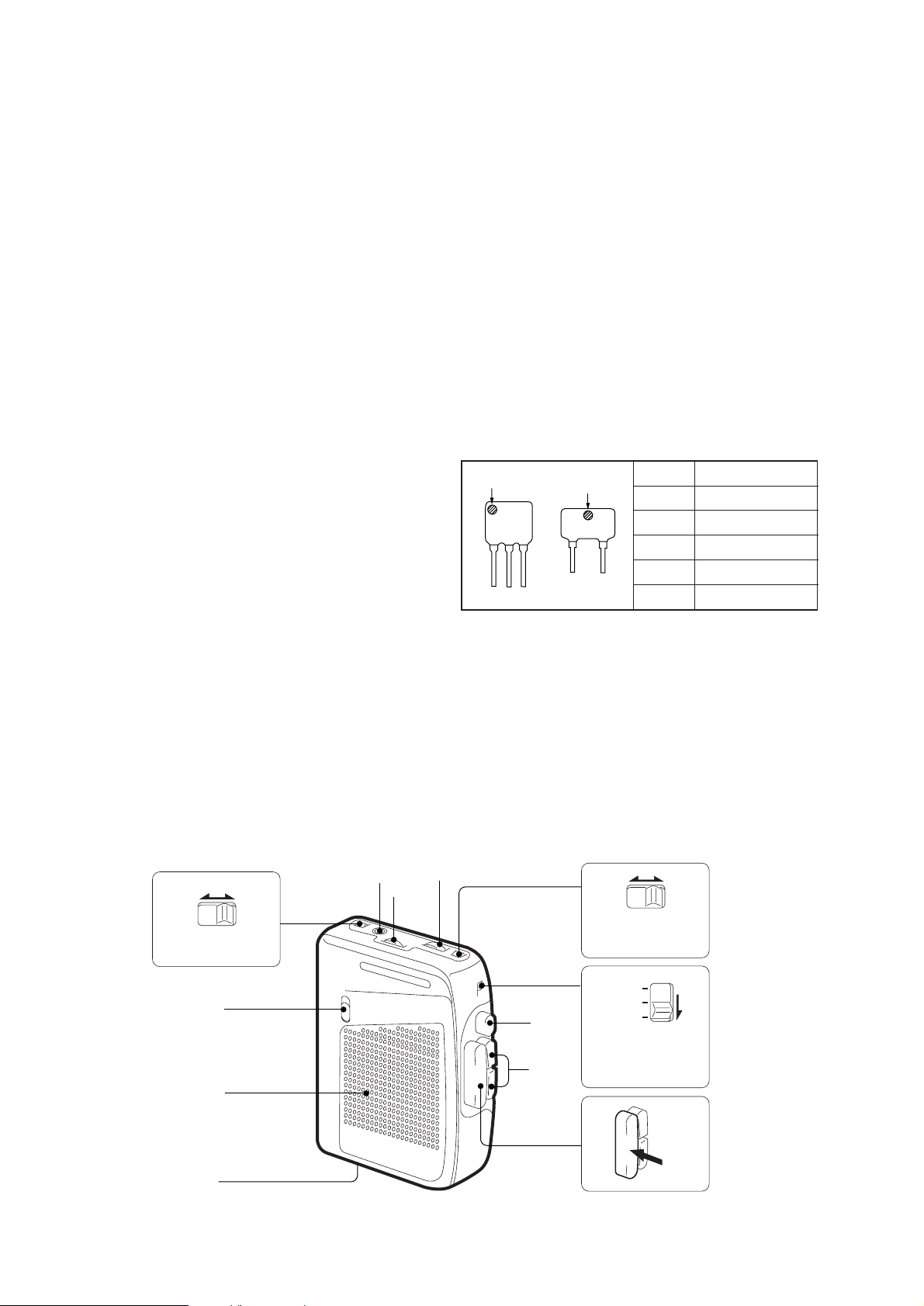
TABLE OF CONTENTS
mark
mark
CF2
X2
Specifications ........................................................................... 1
1. GENERAL
Location and Function of Controls .................................... 2
Flexible Circuit Board Repairing
• Keep the temperature of the soldering iron around 270°C during
repairing.
• Do not touch the soldering iron on the same conductor of the
circuit board (within 3 times).
• Be careful not to apply force on the conductor when soldering or
unsoldering.
2. DISASSEMBLY
2-1. Cabinet (Rear) Removal ............................................. 3
2-2. Cabinet (Front) Removal ............................................ 3
2-3. Main Board, Mechanism Deck Removal ................... 4
2-4. Cassette Holder Sub Assy Removal ........................... 4
2-5. Switch board Removal ............................................... 5
2-6. Dial Pointer Setting .................................................... 5
3. ADJUSTMENTS
3-1. Mechanical Adjustment .............................................. 6
3-2. Electrical Adjustment ................................................. 6
4. DIAGRAMS
4-1. Block Diagram............................................................ 8
4-2. Printed Wiring Boards .............................................. 10
4-3. Schematic Diagram................................................... 15
5. EXPLODED VIEWS
5-1. Cabinet and Board Section ....................................... 19
5-2. Mechanism Deck Section ......................................... 20
6. ELECTRICAL P ARTS LIST ................................21
Notes on chip component replacement
• Never reuse a disconnected chip component.
• Notice that the minus side of a tantalum capacitor may be damaged by heat.
• HOW TO CHANGED THE CERAMIC FILTERS
This model is used two ceramic filters of CF2 and X2.
Y ou must used same type of color marked ceramic filters in order
to meet same specifications.
Therefore, the ceramic filter must changed two pieces together
since it's supply two pieces in one package as a spare parts
Mark Center Frequency
red 10.70MHz
blue 10.67MHz
orange 10.73MHz
black 10.64MHz
white 10.76MHz
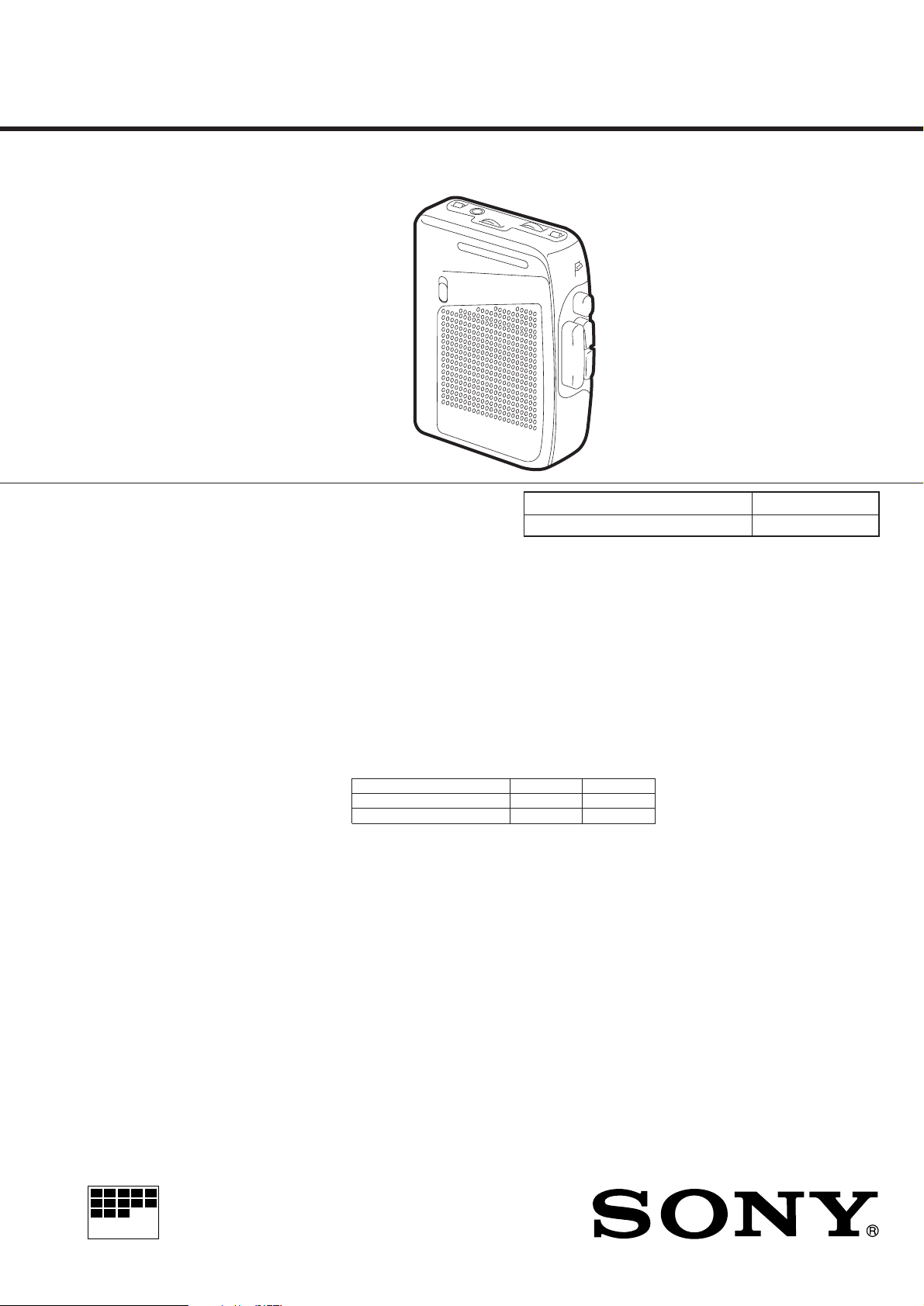
LOCATION AND FUNCTION OF CONTROLS
••
NORM LIMIT
AVLS
SPEAKER
SWITCH
SPEAKER
DC IN 3V
SECTION 1
GENERAL
VOLUME
2
TUNING
p
0 )
••
NORM CrO
METAL
DX LOCAL
FM AM TAPE
(RADIO OFF)
2
/
PLAY
– 2 –
Page 3
SECTION 2
DISASSEMBLY
r
The equipment can be removed using the following procedure.
Set
Cabinet (Rear)
Cabinet (Front)
Note : Follow the disassembly procedure in the numerical order given.
2-1. CABINET (REAR) REMOVAL
1
Main board, Mechanism deck
4
Cassette holder sub assy Switch board
Cassette holder sub assy
2
2
3
3
2-2. CABINET (FRONT) REMOVAL
7
7
7
4
7
7
Cabinet (Rear)
6
6
6
5
8
1
Flexible board
2
Cabinet (Front)
– 3 –
Page 4

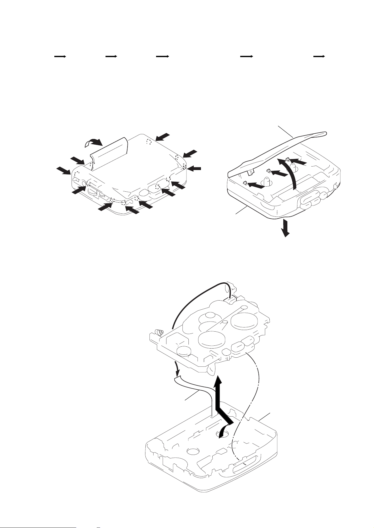
2-3. MAIN BOARD, MECHANISM DECK REMOVAL
k
y
2
Head flexible board
3
Claw
2-4. CASSETTE HOLDER SUB ASSY REMOVAL
4
1
Remove solder
Main board
Mechanism dec
3
Claws
Cabinet (Front)
3
Flexible board
1
2
Cassette holder sub ass
4
NOTE FOR INSTALLATION
The torsion spring will be removed together with the cassette lid that preform the following for installation.
r
TORSION SPRING
1
Attach the torsion spring
as shown in the figure
3
Lift the torsion spring in the arrow
direction and hook it properly
2
Insert the torsion spring
in the hole as shown in the figure.
– 4 –
Page 5

1
Screws
(1.7x3) tapping
Retainer, Speaker
Speaker
Cassette holder sub assy
Switch board
y
)
r
t
SECTION 3
S302
(MD POWER)
S304 - 1
S304
FM
AM
TAPE
RADIO
OFF
RV601
TAPE
SPEED
DC IN 3V
ADJUSTMENTS
WM-P A1
SECTION 4
DIAGRAMS
2-5. SWITCH BOARD REMOVAL
2-6. DIAL POINTER SETTING
2
Align pointer with arrow marked
side as shown in Fig. 1 and then
fit to groove in the order of
a
and b.
3-1. MECHANICAL ADJUSTMENTS
PRECAUTION
1. Clean the following parts with a denatured-alcohol-moistened
swab :
playback head pinch roller
capstan rubber belt
2. Demagnetize the playback head using a head demagnetizer.
3. Do not use a magnetized screwdriver for adjustments.
4. After the adjustments, apply suitable locking compound to the
parts adjusted.
5. The adjustments should be performed with the rated power supply voltage (2.5V) unless otherwise noted.
Torque Measurement
Torque Torque Meter Meter Reading
FWD
CQ-102C
20 – 42 g • cm
(0.28 – 0.58 oz• inch)
FWD less than 2 g • cm
back tension (less than 0.03 oz• inch)
FF, REW CQ-201B
more than 60g • cm
(more than 0.83 oz• inch)
Tape Pulling Force Measurement
Mode Torque Meter Meter Reading
FWD CQ-403A
more than 40 g
(more than 1.42 oz)
3-2. ELECTRICAL ADJUSTMENTS
PRECAUTION
• Specified voltage : 2.5V.
• Switch and control position
TAPE switch : NORM
VOLUME control : maximum
AVLS switch : NORM
T APE SECTION
Test T ape
Type Signal Used for
WS-48A 3kHz, 0dB Tape Speed Adjustment
Tape Speed Adjustment
Procedure :
test tape
WS-48A
(3kHz, 0dB)
set
Play back WS-48A (tape center part) and adjust RV601 so that
the frequency counter reading becomes 3,000 ± 15Hz.
Frequency difference the beginning and the end of the tape
should be within 1.5%.
Adjustment Location :
frequency counter
16
Ω
J302 (phones)
+
–
TUNER SECTION
AM Section
BAND : AM
AM RF signal
generator
30% amplitude modulation by 400Hz
signal.
Output level : as low as possible
FM Section
BAND : FM
LOCAL/DX switch : DX
FM RF signal
generator
22.5kHz frequency deviation by
400Hz signal.
Output level : as low as possible
set
• Repeat the procedures in each adjustment several times, and the
frequency coverage and tracking adjustments should be finally
done by the trimmer capacitors.
Put the lead-wire
antenna close to
the set.
Ω
16
J302 (phones)
µ
0.01 F
level mete
+
–
(ANT TAP
(GND)
AM IF ALIGNMENT
Adjust for a maximum reading on level meter.
T1 1,000kHz
AM FREQUENCY COVERAGE ADJUSTMENT
Adjust for a maximum reading on level meter.
L4 505kHz
CT1–4 1,750kHz
AM TRACKING ADJUSTMENT
Adjust for a maximum reading on level meter.
L1 620kHz
CT1–1 1,400kHz
FM FREQUENCY COVERAGE ADJUSTMENT
Adjust for a maximum reading on level meter.
L3 86.0MHz
CT1–3 109.5MHz
FM TRACKING ADJUSTMENT
Adjust for a maximum reading on level meter.
L2 86.0MHz
CT1–2 109.5MHz
4-1. BLOCK DIAGRAM
Ferrite-rod antenna sub assy
Main board
a
Pointer
3
Ferrite-rod antenna sub ass
[MAIN BOARD] (Side A)
Adjustment Location :
b
Pointer
Fig. 1
Knob (tune)
1
Rotate tune knob fully to arrow direction.
– 5 – – 6 – – 8 –– 7 – – 9 –
Align point
A
(A=B)
B
Align point
RV601
CT1–4 : AM Frequency Coverage Adjustment
CT1–3 : FM Frequency Coverage Adjustment
T1 : AM IF Alignment
L4 : AM Frequency Coverage Adjustmen
L3 : FM Frequency Coverage Adjustment
L2 : FM Tracking Adjustment
CT1–2 : FM Tracking Adjustment
CT1–1 : AM Tracking Adjustment
L1 : AM Tracking Adjustment
• Signal path.
: FM
: PB
Page 6

4-3. SCHEMATIC DIAGRAM
STEREO
DECODER
SWHYS
ST
LED
TU
LED
FM
DET
VCO
PHASE
COM
PHASE
COM
FREQ.
DIVIDER
FM/AM
MONO SW
FM
IF
L
DET
AM
IF
PRE
AF
AM
OSC
FM
OSC
AM
MIX
FM
MIX
FM
RF
AM
RF
AM
DET
AM
AGC
1
24 23 22 21 20 18 17 16 15 14 13
2 3 4 5 6 7 8 9 10 11 12
19
AM RF INFM RF IN
GND1
FM MIX
AM MIX
AGC
VCC2
AM IF IN
FM IF IN
GND2
TUN LED
ST LED
QUAD
FM RF OUT
VCC1
FM OSC
AM OSC
DET OUT
MPX IN
LPF1
LPF2
VCO
L OUT
R OUT
r
IC BLOCK DIAGRAM
IC1 TA8122AF
WM-PA1
Note:
• All capacitors are in µF unless otherwise noted. pF: µµF
50 WV or less are not indicated except for electrolytics and
tantalums.
• All resistors are in Ω and 1/
specified.
¢
•
: internal component.
4
W or less unless otherwise
• : B+ Line.
• : adjustment for repair.
• Power voltage is dc 3V and fed with regulated dc power
supply from external power voltage jack (J301).
• Voltages are dc with respect to ground under no-signal
(detuned) conditions.
no mark : FM
( ) : AM
< > : PLAY
• Voltages are taken with a VOM (Input impedance 10 MΩ).
Voltage variations may be noted due to normal production
tolerances.
• Signal path.
: FM
: PB
– 15 – – 16 – – 18 –– 17 –
Page 7

NOTE :
• -XX, -X mean standardized parts, so they
may have some difference from the original
one.
• Items marked “ * ”are not stocked since they
are seldom required for routine service. Some
delay should be anticipated when ordering
these items.
5-1. CABINET AND BOARD SECTION
12
11
SP1
SECTION 5
EXPLODED VIEWS
• The mechanical parts with no reference
number in the exploded views are not
supplied.
• Accessories and packing materials are given
in the last of this parts list.
13
14
15
16
L1
19
10
9
17
18
20
22
8
7
7
5
6
4
3
2
21
1
Ref. No. Part No. Description Remark Ref. No. Part No. Description Remark
1 X-3374-460-1 CABINET (REAR) SUB ASSY
2 3-910-896-01 GROUND, MOTOR
3 3-933-647-01 BUTTON (STOP)
4 3-933-644-01 BUTTON (FF)
5 3-933-643-01 BUTTON (REW)
6 3-933-646-01 BUTTON (PLAY)
7 3-318-382-01 SCREW (1.7X3), TAPPING
8 3-017-324-01 RETAINER, SPEAKER
9 1-667-057-11 FLEXIBLE BOARD
* 10 1-667-779-11 SWITCH BOARD
11 X-3374-461-1 HOLDER SUB ASSY, CASSETTE
12 3-017-323-01 KNOB (SW)
13 3-018-931-01 SPRING, TORSION
14 3-937-353-01 CABINET (FRONT) (CF-O)
15 3-364-675-01 SPRING (CASSETTE)
16 3-933-678-01 POINTER
17 3-933-642-01 TERMINAL (+), BATTERY
18 3-933-675-01 GEAR (TUNE)
19 3-910-902-12 KNOB (TUNE)
20 A-3016-981-A MAIN BOARD, COMPLETE
21 3-937-356-01 LID, BATT
22 3-910-895-01 TERMINAL (–), BATTERY
L1 X-3371-847-1 ANTENNA SUB ASSY, FERRITE-ROD
SP1 1-505-794-11 SPEAKER
– 19 –
Page 8

5-2. MECHANISM DECK SECTION (MF-WMFX103-48CY)
60
51
59
61
58
HP901
62
not
supplied
52
not
supplied
53
54
55
M901
57
56
Ref. No. Part No. Description Remark Ref. No. Part No. Description Remark
51 X-3367-902-1 ARM (N) ASSY, PINCH
52 3-364-328-01 SPRING, COMPRESSION
53 3-910-635-01 SCREW
54 3-910-647-01 LEVER (PR/O), PLAY
55 X-3368-729-1 CHASSIS ASSY
56 3-354-868-01 BELT
57 3-352-758-21 SCREW (M1.7), TOOTHED LOCK
58 3-909-727-01 GEAR (REVERSE)
59 3-364-320-01 GEAR (S REEL)
60 3-910-640-01 GEAR (T REEL)
61 3-321-483-11 RING, RETAINING
62 X-3367-905-1 CLUTCH ASSY
HP901 1-500-115-11 HEAD, MAGNETIC (PLAYBACK)
M901 1-698-353-11 MOTOR, DC (REEL, CAPSTAN)
– 20 –
Page 9

SECTION 6
ELECTRICAL PARTS LIST
NOTE :
• Due to standardization, replacements in the
parts list may be different from the parts
specified in the diagrams or the components
used on the set.
• -XX, -X mean standardized parts, so they
may have some difference from the original
one.
• RESISTORS
All resistors are in ohms
METAL : Metal-film resistor
METAL OXIDE :Metal oxide-film resistor
F : nonflammable
Ref. No. Part No. Description Remark Ref. No. Part No. Description Remark
A-3016-981-A MAIN BOARD, COMPLETE
*********************
• Items marked “ * ”are not stocked since they
are seldom required for routine service. Some
delay should be anticipated when ordering
these items.
• SEMICONDUCTORS
In each case, u : µ , for example :
uA.... : µ A.... , uPA.... : µ PA....
uPB.... : µ PB.... , uPC.... : µ PC....
uPD.... : µ PD....
• CAPACITORS
uF : µ F
• COILS
uH : µ H
C308 1-126-157-11 ELECT 10uF 20% 16V
C309 1-163-038-91 CERAMIC CHIP 0.1uF 25V
When indicating parts by reference number, please include the board.
MAIN
3-910-895-01 TERMINAL (–), BATTERY
3-933-642-01 TERMINAL (+), BATTERY
< CAPACITOR >
C1 1-163-083-00 CERAMIC CHIP 1PF 50V
C2 1-163-099-00 CERAMIC CHIP 18PF 5% 50V
C3 1-163-101-00 CERAMIC CHIP 22PF 5% 50V
C4 1-163-089-00 CERAMIC CHIP 6PF 50V
C5 1-163-117-00 CERAMIC CHIP 100PF 5% 50V
C6 1-163-003-11 CERAMIC CHIP 330PF 10% 50V
C7 1-164-005-11 CERAMIC CHIP 0.47uF 25V
C8 1-163-038-91 CERAMIC CHIP 0.1uF 25V
C9 1-163-038-91 CERAMIC CHIP 0.1uF 25V
C10 1-163-038-91 CERAMIC CHIP 0.1uF 25V
C11 1-163-117-00 CERAMIC CHIP 100PF 5% 50V
C12 1-163-117-00 CERAMIC CHIP 100PF 5% 50V
C14 1-126-153-11 ELECT 22uF 20% 6.3V
C15 1-163-078-11 CERAMIC CHIP 0.033uF 10% 25V
C16 1-163-063-91 CERAMIC CHIP 0.022uF 10% 50V
C17 1-126-154-11 ELECT 47uF 20% 6.3V
C18 1-163-037-11 CERAMIC CHIP 0.022uF 10% 25V
C19 1-163-037-11 CERAMIC CHIP 0.022uF 10% 25V
C24 1-164-234-11 CERAMIC CHIP 1uF 10V
C101 1-163-007-11 CERAMIC CHIP 680PF 10% 50V
C102 1-126-153-11 ELECT 22uF 20% 6.3V
C103 1-163-019-00 CERAMIC CHIP 0.0068uF 10% 50V
C104 1-164-234-11 CERAMIC CHIP 1uF 10V
C105 1-163-117-00 CERAMIC CHIP 100PF 5% 50V
C106 1-163-009-11 CERAMIC CHIP 0.001uF 10% 50V
C310 1-164-234-11 CERAMIC CHIP 1uF 10V
C311 1-164-234-11 CERAMIC CHIP 1uF 10V
C312 1-163-009-11 CERAMIC CHIP 0.001uF 10% 50V
C313 1-163-038-91 CERAMIC CHIP 0.1uF 25V
C314 1-163-117-00 CERAMIC CHIP 100PF 10% 50V
C401 1-163-117-00 CERAMIC CHIP 100PF 10% 50V
C402 1-163-021-91 CERAMIC CHIP 0.01uF 5% 50V
C403 1-163-017-00 CERAMIC CHIP 0.0047uF 5% 50V
C404 1-164-234-11 CERAMIC CHIP 1uF 10V
C405 1-163-017-00 CERAMIC CHIP 0.0047uF 5% 50V
C406 1-163-017-00 CERAMIC CHIP 0.0047uF 5% 50V
C407 1-126-157-11 ELECT 10uF 20% 16V
C408 1-164-222-11 CERAMIC CHIP 0.22uF 25V
C409 1-163-038-91 CERAMIC CHIP 0.1uF 25V
C410 1-126-176-11 ELECT 220uF 20% 4V
C411 1-164-234-11 CERAMIC CHIP 1uF 10V
C412 1-164-234-11 CERAMIC CHIP 1uF 10V
C413 1-163-038-91 CERAMIC CHIP 0.1uF 25V
C601 1-126-154-11 ELECT 47uF 20% 6.3V
C602 1-164-005-11 CERAMIC CHIP 0.47uF 25V
C603 1-164-505-11 CERAMIC CHIP 2.2uF 16V
C604 1-164-232-11 CERAMIC CHIP 0.01uF 50V
C605 1-164-005-11 CERAMIC CHIP 0.47uF 25V
< FILTER >
CF1 1-527-870-00 FILTER
CF2 1-578-672-71 FILTER, CRYSTAL
< CONNECTOR >
C201 1-163-007-11 CERAMIC CHIP 680PF 10% 50V
C202 1-126-153-11 ELECT 22uF 20% 6.3V
C203 1-163-019-00 CERAMIC CHIP 0.0068uF 10% 50V
C204 1-164-234-11 CERAMIC CHIP 1uF 10V
C205 1-163-117-00 CERAMIC CHIP 100PF 5% 50V
C206 1-163-009-11 CERAMIC CHIP 0.001uF 10% 50V
C301 1-164-505-11 CERAMIC CHIP 2.2uF 16V
C302 1-126-153-11 ELECT 22uF 20% 6.3V
C303 1-163-038-91 CERAMIC CHIP 0.1uF 25V
C304 1-163-038-91 CERAMIC CHIP 0.1uF 25V
C305 1-163-009-11 CERAMIC CHIP 0.001uF 10% 50V
C306 1-126-176-11 ELECT 220uF 20% 4V
C307 1-164-505-11 CERAMIC CHIP 2.2uF 16V
CN301 1-569-252-21 HOUSING, CONNECTOR (FPC) 5P
CN401 1-565-289-11 HOUSING, CONNECTOR 7P
< TRIMMER >
CT1 1-141-567-11 CAP, VAR (TUNING)
< VARIABLE CAPACITOR >
CV1 1-141-567-11 CAP, VAR (TUNING)
< IC >
IC1 8-759-230-39 IC TA8122AF
IC301 8-759-497-06 MM1316AFBE
– 21 –
Page 10

WM-PA1
MAIN SWITCH
Ref. No. Part No. Description Remark Ref. No. Part No. Description Remark
IC401 8-759-702-02 IC NJM062M
< JACK >
J301 1-750-061-11 JACK,DC(POLARITY UNIFIED TYPE)(DC IN 3V)
J302 1-565-287-11 JACK (2)
R410 1-216-001-00 METAL CHIP 10 5% 1/10W
R411 1-216-097-91 METAL GLAZE 100K 5% 1/10W
R601 1-217-905-11 METAL GLAZE 1.5 5% 1/10W
R602 1-216-298-00 METAL CHIP 2.2 5% 1/10W
R603 1-216-043-91 METAL GLAZE 560 5% 1/10W
< JUMPER RESISTOR >
JC1 1-216-295-00 METAL CHIP 0 5% 1/10W
JC4 1-216-295-00 METAL CHIP 0 5% 1/10W
JC5 1-216-295-00 METAL CHIP 0 5% 1/10W
< COIL >
L1 X-3371-847-1 ANTENNA SUB ASSY, FERRITE-ROD
L2 1-460-120-11 COIL (WITH CORE)
L3 1-403-696-11 COIL (WITH CORE)
L4 1-406-408-11 COIL (OSC)
L101 1-500-245-11 INDUCTOR
L201 1-500-245-11 INDUCTOR
L301 1-412-006-31 INDUCTOR CHIP 10uH
< TRANSISTOR >
Q2 8-729-216-22 TRANSISTOR 2SA1162-G
Q301 8-729-402-13 TRANSISTOR XN1501
Q302 8-729-216-22 TRANSISTOR 2SA1162-G
Q401 8-729-216-22 TRANSISTOR 2SA1162-G
Q402 8-729-207-73 TRANSISTOR RN2407
Q403 8-729-230-49 TRANSISTOR 2SC2712-YG
< RESISTOR >
R1 1-216-009-00 METAL CHIP 22 5% 1/10W
R2 1-216-081-00 METAL CHIP 22K 5% 1/10W
R3 1-216-077-00 METAL CHIP 15K 5% 1/10W
R4 1-216-077-00 METAL CHIP 15K 5% 1/10W
R5 1-216-037-00 METAL CHIP 330 5% 1/10W
R6 1-216-065-00 METAL CHIP 4.7K 5% 1/10W
R7 1-216-065-00 METAL CHIP 4.7K 5% 1/10W
R101 1-216-006-11 METAL GLAZE 16 5% 1/10W
R102 1-216-077-00 METAL CHIP 15K 5% 1/10W
R201 1-216-006-11 METAL GLAZE 16 5% 1/10W
R202 1-216-077-00 METAL CHIP 15K 5% 1/10W
R301 1-216-089-91 METAL GLAZE 47K 5% 1/10W
R302 1-216-073-00 METAL CHIP 10K 5% 1/10W
R304 1-216-308-00 METAL CHIP 4.7 5% 1/10W
R305 1-216-081-00 METAL CHIP 22K 5% 1/10W
R306 1-216-073-00 METAL CHIP 10K 5% 1/10W
R322 1-216-097-91 METAL GLAZE 100K 5% 1/10W
R401 1-216-097-91 METAL GLAZE 100K 5% 1/10W
R402 1-216-097-91 METAL GLAZE 100K 5% 1/10W
R403 1-216-113-00 METAL CHIP 470K 5% 1/10W
R404 1-216-049-91 METAL CHIP 1K 5% 1/10W
R405 1-216-057-00 METAL CHIP 2.2K 5% 1/10W
R406 1-216-049-91 METAL GLAZE 1K 5% 1/10W
R407 1-216-057-00 METAL CHIP 2.2K 5% 1/10W
R408 1-216-089-91 METAL GLAZE 47K 5% 1/10W
< VARIABLE RESISTOR >
RV301 1-225-578-11 RES, VAR, CARBON (∑ VOLUME)
RV601 1-225-252-11 RES, ADJ, CARBON 470 (TAPE SPEED)
< SWITCH >
S302 1-571-986-11 SWITCH, LEAF (MD POWER)
S303 1-692-298-11 SWITCH, SLIDE (LOCAL/DX, NORM/METAL)
S304 1-692-299-11 SWITCH, SLIDE (FM, AM, TAPE RADIO OFF)
S305 1-692-898-11 SWITCH, SLIDE (AVLS)
< TRANSFORMER >
T1 1-404-949-11 TRANSFORMER, IF
< THERMISTOR >
TH601 1-809-279-11 THERMISTOR, POSITIVE
TH602 1-810-764-11 THERMISTOR, POSITIVE
< FILTER >
X1 1-577-091-11 OSCILLATOR, CRYSTAL
X2 1-578-672-71 FILTER, CRYSTAL
************************************************************
* 1-667-779-11 SWITCH BOARD
*************
1-667-057-11 FLEXIBLE BOARD
< SWITCH >
S401 1-572-922-11 SWITCH, SLIDE (SPEAKER)
************************************************************
MISCELLANEOUS
**************
9 1-667-057-11 FLEXIBLE BOARD
HP901 1-500-115-11 HEAD, MAGNETIC (PLAYBACK)
L1 X-3371-847-1 ANTENNA SUB ASSY, FERRITE-ROD
M901 1-698-353-11 MOTOR, DC (REEL, CAPSTAN)
SP1 1-505-794-11 SPEAKER
************************************************************
ACCESSORIES & PACKING MATERIALS
********************************
3-861-236-21 MANUAL, INSTRUCTION (SPANISH,
PORTUGUESE)
8-953-130-90 HEADPHONE MDR-E801//K SET
X-3372-629-1 CLIP ASSY, BELT
R409 1-216-089-91 METAL GLAZE 47K 5% 1/10W
Sony Corporation
9-923-266-11
Personal A&V Products Company
– 22 –
Printed in Singapore © 1997.10
97J027025-1
Published by Quality Engineering Dept.
(Shibaura)
 Loading...