

Sony WMGX-410 Service manual
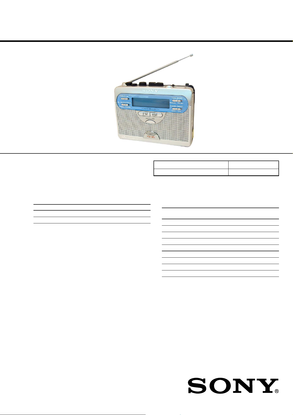
WM-GX410
SERVICE MANUAL
Ver 1.0 2004. 03
Model Name Using Simillar Mechanism NEW
Tape Transport Mechanism Type MT-WMGX410-175
SPECIFICATIONS
Canadian Model
AEP Model
E Model
Chinese Model
Tourist Model
Frequency range
Area* FM (MHz) AM(kHz)
AEP, E, Chinese 7.5 - 108 531 - 1 602
Canada, Tourist 87.5 - 108 530 - 1 710
Frequency response Playback: 40 - 15 000 Hz
Recording: 100 - 8 000 Hz
Input Microphone (MIC) jack
Output Headphones (i) jack
Load impedance 8 - 300 Ω
Power requirements 3 V DC: batteries R6 (size AA) x 2
External DC 3V power sources
Power output Speaker 500 mW + 500 mW
(JEITA*)
Dimensions (w/h/d) Approx. 112.0x 82.5 x 35.0 mm
(4 1/2 x 3 1/4 x 1 7/16 inches), excl.
projecting parts and controls
Mass Approx. 200 g (7.1oz)
(main unit only)
Supplied accessories Stereo headphones or earphones (1)
Sony dry battery R6P(SR) (2)
(“Sony World Model” only)
Design and specifications are subject to change without notice.
Battery life* (Approx. hours)
Sony alkaline LR6(SG)** Sony
R6P(SR)
(using headphones/earphones)
playback 24 6
radio 48 15
mic recording 20 4.5
radio recording 12 3
(using the speakers)
playback 10 2.5
radio 17.5 5
radio recording 6.5 1
*Measured value by the standard of JEIT A (Japan Electronics and
Information T echnology Industries Association). (Using a Sony
HF series cassette tape)
** When using Sony LR6 (SG) alkaline dry batteries (producedin
Japan).
Note
The battery life may be shorter depending on the operating ondition,
the surrounding temperature and battery type.
9-877-585-01
2004C02-1
© 2004.03
RADIO CASSETTE-CORDER
Sony Corporation
Personal Audio Company
Published by Sony Engineering Corporation
WM-GX410
Flexible Circuit Board Repairing
• Keep the temperature of the soldering iron around 270°C
during repairing.
• Do not touch the soldering iron on the same conductor of the
circuit board (within 3 times).
• Be careful not to apply force on the conductor when soldering
or unsoldering.
Notes on chip component replacement
• Never reuse a disconnected chip component.
• Notice that the minus side of a tantalum capacitor may be
damaged by heat.
TABLE OF CONTENTS
Specifications ............................................................................ 1
1. GENERAL
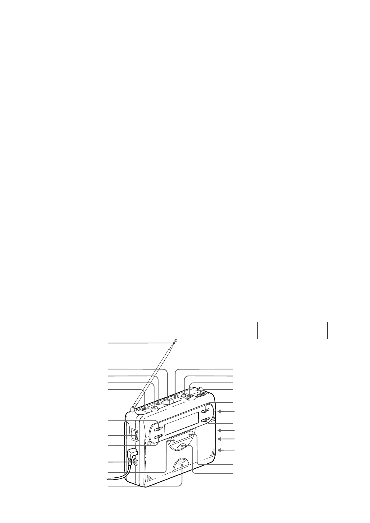
Location of Parts and Controls ........................................2
2. DISASSEMBLY
2-1. Disassembly Flow .................................................... 3
2-2. Cabinet (Center), cabinet Front Assy....................... 3
2-3. Main Board .............................................................. 4
2-4. Mechanism Deck (MT-WMFX410-175) ................. 4
2-5. Cassette Holder Sub Assy ........................................ 5
2-6. Sub Board................................................................. 5
2-7. Rec/PB/ Erase head (HRPE301), Belt (AR),
Capstan/Reel Motor (M601) ................................... 6
3. ADJUSTMENTS
3-1. Mechanical Adjustments.......................................... 7
3-2. Electrical Adjustments ............................................. 7
SECTION 1
GENERAL
Antenna
4. DIAGRAMS
4-1.IC Pin Function Descriptions .................................... 10
4-2. Block Diagrams –Tape Section– .............................. 11
4-3. Block Diagrams –Tuner Section– ............................ 12
4-4. Printed Wiring Board –Main Section (Side A)– ...... 13
Printed Wiring Board –Main Section (Side B)–.......14
4-5. Schematic Diagram –Main Section (1/2)–............... 15
4-6. Schematic Diagram –Main Section (2/2)–............... 16
4-7. Printed Wiring Board –Sub Section (Side A)–.........17
4-8. Printed Wiring Board –Sub Section (Side B)–......... 18
4-9. Schematic Diagram –Sub Section–.......................... 19
4-10.IC Block Diagrams..................................................20
5. EXPLODED VIEWS
5-1. Cabinet (Rear) Section ............................................. 22
5-2. Cassette Lid Section................................................. 23
5-3. Mechanism Section-1 (MT-WMGX410-175)..........24
5-4. Mechanism Section-2 (MT-WMGX410-175)..........25
6. ELECTRICAL PARTS LIST .................................. 26
This section is extracted
from instruction manual.
FF/CUEREW/REVIEW
PLAY**
STOP
REC
HOLD
VOL*
REC TIME/PLAY MODE
MIC (PLUG IN POWER)**
FM
Flat Mic
* There is a tactile dot beside VOL on the main unit to show the direction to turn
up the volume.
2
** The button or jack has a tactile dot.
DIR
TUNING/ENTER
PAUSE
TUNE MODE
FM MODE•MONO/ST
FM MODE•LOCAL/DX
SOUND BOOST
AVLS
ISS
DC IN 3V
AM
RADIO OFF
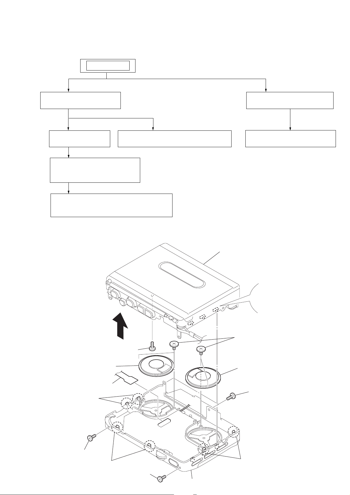
• This set can be disassembled in the order shown below.
2-1. DISASSEMBLY FLOW
SET
WM-GX410
SECTION 2
DISASSEMBLY
2-2. CABINET (CENTER)
(Page 3)
2-3. MAIN BOARD
(Page 4)
2-5. CASSETTE HOLDER SUB ASSY
(Page 5)
2-4. MECHANISM DECK
(MT-WMFX410-175)
(Page 4)
2-7. REC/PB/ERASE HEAD (HRPE301),
BELT (AR), CAPSTAN/REEL MOTOR
(M601) (Page 6)
Note: Follow the disassembly procedure in the numerical order given.
2-2. CABINET (CENTER), CABINET FRONT ASSY
2-2. CABINET FRONT ASSY
(Page 3)
2-6. SUB BOARD
(Page 5)
cabinet (center)
8
screw (M1.4 toothed lock)
SP401
7
fiexible board (CN301)
5
two claws
2
screw (M1.4)
4
two claws
6
2
screw (M1.4)
Note on installation
Align three switches and
three knobs
9
four screws (tapping B2.0)
SP402
1
two screws
3
two claws
cabinet front assy
3
WM-GX410
)
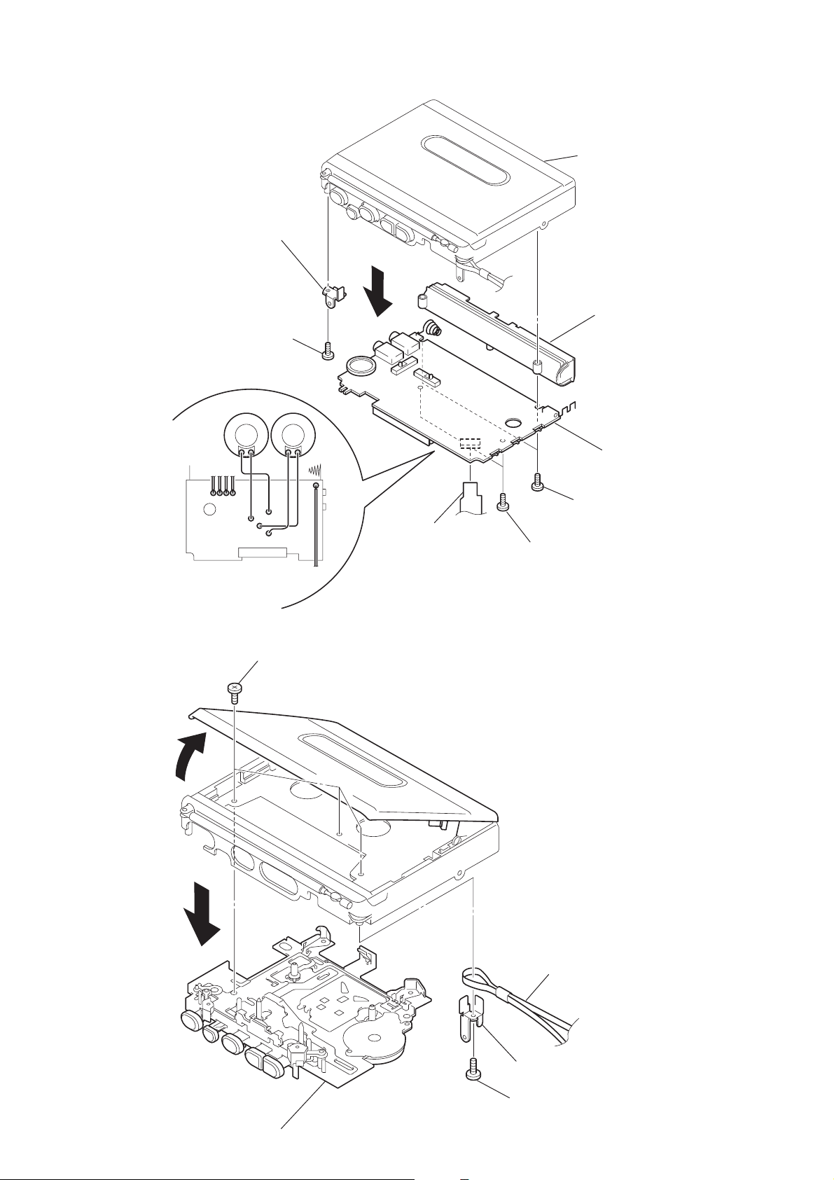
2-3. MAIN BOARD
2
remove nine soldering
6
plate connector (L)
5
screw
7
cabinet (center)
8
joint cover
MAIN board
2-4. MECHANISM DECK (MT-WMFX410-175)
2
three screws (IB lock)
1
6
1
flexible board
(CN305)
4
two screws
3
two screws (M1.4 toothed lock)
5
hand strap
4
plate, connector (R
3
screw
mechanism deck (MT-WMGX410-175)
4
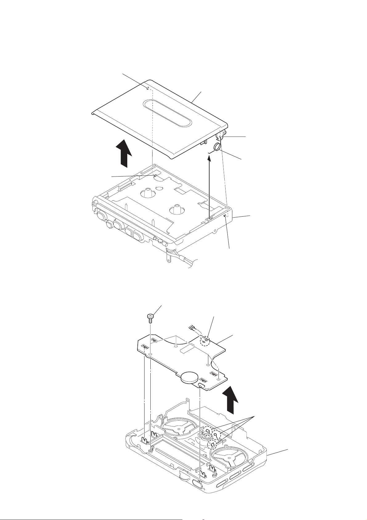
2-5. CASSETTE HOLDER SUB ASSY
n
y
1
remove from projection
cassette holder sub assy
2
remove from projectio
WM-GX410
projection
2-6. SUB BOARD
3
2
four screws
4
spring, torstion
cabinet (center)
projection
1
remove two soldering
sub board
Note on installation
Align five switches and
five knobs
4
3
three claws
cabinet front ass
5

WM-GX410
2-7. REC/PB/ERASE HEAD (HRPE301), BELT (AR), CAPSTAN/REEL MOTOR (M601)
Attaching belt (AR)
3
belt (AR)
1
two screws (M1.4)
4
two screws (M1.4)
5
M601 (CAPSTAN/REEL motor)
2
HRPE301 (REC/PB/ERASE head)
6
r
SECTION 3
R607
R601
RV602: Tape Speed Adjustment
(4.8cm/s)
RV601: Tape Speed Adjustment
(2.4cm/s)
RV601
RV602
[MAIN BOARD] (SIDE B)
ADJUSTMENTS
WM-GX410
3-1. MECHANICAL ADJUSTMENTS
1. Clean the following parts with a denatured alcohol-moistened
2. Demagnetize the record/playback/erase head with a head
3. Do not use a magnetized screwdriver for the adjustments.
4. After the adjustments, apply suitable locking compound to
5. The adjustments should be performed with the rated power
6. Power supply voltage : 3V DC.
Torque Measurement
Forward/Reverse CQ-102C (20 to 40 g • cm)
Back Tension
Back Tension
Fast Forward
and Rewind
3-2. ELECTRICAL ADJUSTMENTS
Note:
1. Supplied voltage: 3 V (DC)
2. Switch and control position
PRECAUTION
swab :
record/playback/erase head pinch roller
capstan rubber belts
demagnetizer.
the parts adjusted.
supply voltage unless otherwise noted.
Mode Torque Meter Meter Reading
1.97 to 3.92 mN • m
(0.28 to 0.55 oz• inch)
Forward
CQ-102C (0.5 to 5.0 g • cm)
Reverse
CQ-102RC (0.5 to 5.0 g • cm)
CQ-201B (50 g • cm)
0.05 to 0.49 mN • m
(0.007 to 0.07 oz• inch)
0.05 to 0.49 mN • m
(0.007 to 0.07 oz• inch)
more than 4.90 mN • m
(0.7 oz• inch)
VOLUME control : output level < > :AEP
FM -20dBm <-30dBm>
AM-30dBm <-40dBm>
AVLS switch : NORM
REC TIME/PLAY MODE switch : NORMAL
ISS switch : 1
1. Set REC TIME switch (S706) to NORMAL (4.8cm/s).
2. Play back the center portion of tape in REVmode, adjust R V602
so that the reading on the frequency counter becomes 3,000 Hz.
3. Set REC TIME switch (S706) to DOUBLE (2.4cm/s).
4. Play back the center portion of tape in REVmode, adjust R V601
so that the reading on the frequency counter becomes 1,500 Hz.
Specifications:
NORMAL (4.8cm/s) : 2,985Hz - 3,015Hz
DOUBLE (2.4cm/s) : 1,493Hz - 1,507Hz
5. Confirm the frequency difference between the beginning and
the end of tape should be 1.5%.
NORMAL (4.8cm/s) : 45Hz
DOUBLE (2.4cm/s) : 22.5Hz
4
RV602
C606
R605
R609
06
R423
R340
C339
R341
C221
R344
R354
R338
B
E
B
C336
C337
Q342
Q335
C
C
R337
C338
R339
C333
R606
R336
Q336
RV601
C332
TH601
C70
Q334
C410
R309
R3
9
C86
R335
CN303
1
FB303
C340
Adjustment Location: Main board (See page 9)
TAPE DECK SECTION 0 dB = 0.775 V
Test T ape
Type Signal Used for
WS-48A 3 kHz, 0 dB Tape Speed Adjustment
Tape Speed Adjustment
Procedure:
test tape
WS-48A
(3kHz, 0dB)
frequency counte
16Ω
set
i headphone jack (J401)
7
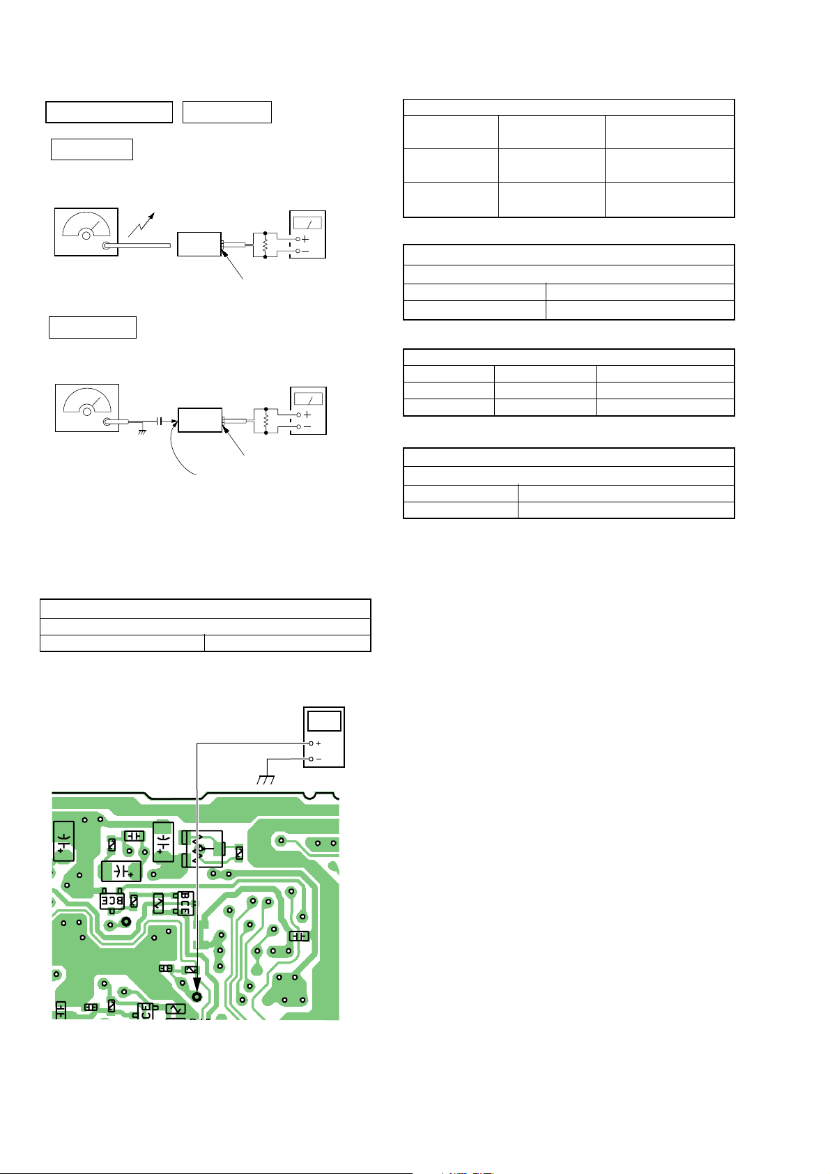
WM-GX410
)
)
TP333
(LPF)
TP8
TP3
Q308
C43
R313
Q307
R3
C71
C17
R6
R312
C16
C8
C12
R18
Q3
RV1
C31
R22
r
±
TUNER SECTION 0 dB = 1 µV
AM Section
FUNCTION switch: AM
AM RF SSG
30% amplitude modulation by
400Hz signal.
Output level : as low as possible
Put the lead-wire
antenna close to
the set.
set
level meter
Ω
16
i
headphone jack (J401
FM Section
FUNCTION switch: FM
FM RF SSG
0.01
µ
F
set
30% amplitude
modulation by
1kHz signal.
Deviation : 75kHz
Output level : as low
as possible
main board
TAP66
• Repeat the procedures in each adjustment several times, and
the frequency coverage and tracking adjustments should be
finally done by the trimmer capacitors.
AM IF ADJUSTMENT
Adjust for a maximum reading on level meter.
RV2 999 kHz <1,000kHz>
level meter
Ω
16
i
headphone jack (J401
(side B)
no mark : 9kHz step
< > : 10kHz step
AM FREQUENCY COVERAGE ADJUSTMENT
Adjust parts Frequency
L7
Confirmation
AM TRACKING ADJUSTMENT
<530kHz>
531kHz
<1,710kHz>
1,602kHz
Reading on digtal
voltmeter
1.1 ± 0.4V
5.0 ± 0.6V
Adjustment for a maximum reading on level meter.
L3 <620 kHz> 621 kHz
CT1 <1,400 kHz> 1,404 kHz
FM FREQUENCY COVERAGE CONFIRMATION
Frequency display Reading on digtal voltmeter
Confirmation 87.5 MHz Standard value : 4.2 ± 0.5 V
Confirmation 108 MHz 9.1 ± 0.5 V
FM TRACKING ADJUSTMENT
Adjustment for a maximum reading on level meter.
L4 87.5 MHz
Confirmation 108 MHz
Adjustment Location: Main board (See page 9)
[MAIN BOARD] (SIDE A)
8
TP (LPF)
digital voltmete
(DC range)
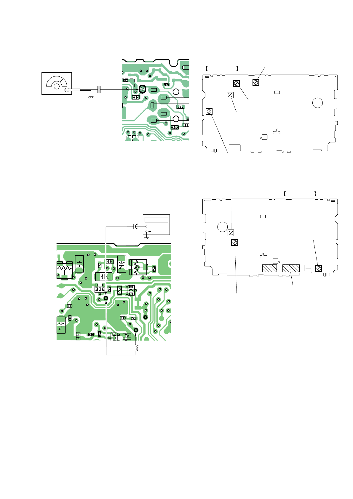
WM-GX410
TP(LPF)
TP8
Q308
C43
R313
Q307
R3
C56
C17
R6
C89
R312
C16
C8
C12
R18
Q3
RV1
C31
RV2
C49
R22
P
2
FM VCO Adjustment
Procedure:
FM RF SSG
0.01
µ
Carrier frequency : 98MHz
Deviation : None
Output level : 562
µ
TAP66
F
(ANT)
V (55dB)
[MAIN BOARD] (SIDE B)
ND
C905
CND
908
4
-3
C920
C40
S302
REC
t
PB
-4
TAP66
TAP66
FB306
FB305
C35
1. Connect the resistor 10kΩ between TP8 and TP(LPF).
2. Connect the frequency counter to TP8 (IC8 7 pin).
3. Set FUNCTION switch to FM.
4. Tune the set in 98MHz.
5. Adjust RV1 so that the reading on the frequency counter becomes 76 kHz.
Specifications: 75 kHz - 77 kHz
frequency
counter
µ
F
1
+
TP8
(IC1 7 pin)
+
Adjustment Location:
MAIN BOARD (SIDE A)
T
RV2 : AM IF adjustment
L4 : FM Tracking Adjustment
C5
L7 : AM Frequency
coverage
adjustment
RV602 : Tape Speed Adjustment (4.8cm/s)
RV1 : FM VCO adjustment
MAIN BOARD (SIDE B)
CT1 :
AM T rac king Adjustment
[MAIN BOARD]
(SIDE A)
Adjustment Location: Main board (See page 9)
10k
L3 : AM Tracking Adjustment
RV601: Tape Speed Adjustment (2.4cm/s)
Ω
9

WM-GX410
SECTION 4
DIAGRAMS
4-1. IC Pin Function Descriptions IC701 (SYSTEM CONTROL/LCD DRIVE) LC723483 W-9C33-E
Pin No. Pin name I/O Description
1 XOUT O Connected to 75kHz Crystal oscillator
2 TEST 2 I For Test (Connected to GND)
3 MECHA REC I REC mode signal input
4 to 6 PA3 to 1 I Control key inputs
7 KO2 O Key source signal output
8 KO1 O Key source signal output
9 REC CTRL O REC control signal output L: REC
10 AMP ON O Power amplifier on/off control signal output
11 SD I SD input
12 COMP I COMP input
13 PUSH I Tuning dial (S701) common switch signal input
14 MECHA TAPE I Tape on/off detection signal input
15 RADIO ON O Radio on/off control signal output
16 BAND O Band select signal output
17 TUNING-B I Tuning dial (S701) B phase signal input
18 TUNING-A I Tuning dial (S701) A phase signal input
19 MUTE O Mute signal output
20 BEEP O Beep signal output
21 BACK UP VOLTAGE I Back-up voltage detection signal input
22 BATT LEVEL I Battery voltage detection signal input
23 VERSION I Destination select signal input
24 GND — Ground terminal
25 TUNER MODE INPUT I Tuning mode select switch (S707) signal input
26 2X INPUT I Tape speed select switch (S706) signal input
27 PAUSE I Pause switch (S702) signal input
28 HOLD I HOLD switch (S705) signal input
29 SHUTDOWN O Not used (open)
30 MOTOR BRAKE O Motor brake control signal output
31 MOTOR CTL O Motor control signal output
32 to 44 S13 to S1 O LCD driver segment output terminal
45 to 48 COM4 to 1 O LCD driver common output terminal
49 TU O Output for tuning voltage generator
50 to 53 DBR4 to 1 I For LCD power supply booster
54 RESET I System reset signal input
55 HCTR NC — Not used (open)
56 VDD — Power supply terminal
57 FM IN I FM VCO input
58 AM IN I AM VCO input
59 GND — Ground terminal
60 E0 O Tuning signal (PWM) output
61 AIN I LPF amplifier input
62 AOUT O LPF amplifier output
63 TEST 1 I For test (connected to ground)
64 XIN I Connected to 75kHz Crystal oscillator
10
 Loading...