

Sony WMGX-400 Service manual
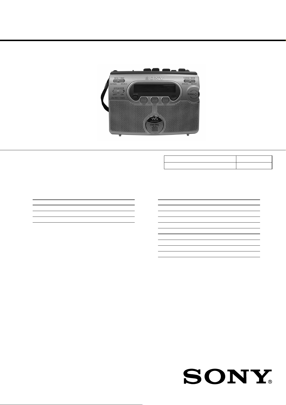
WM-GX400
SERVICE MANUAL
Ver 1.0 2001.03
SPECIFICATIONS
Canadian Model
AEP Model
E Model
Chinese Model
Tourist Model
Model Name Using Similar Mechanism NEW
Tape Transport Mechanism Type MT-WMGX400-175
Frequency range
Area* FM (MHz) AM (kHz)
AEP, E, Chineses model 87.5 - 108 531 - 1 602
US, Canadian model 87.5 - 108 530 - 1 710
Tourist model 76 - 90 531 - 1 710
* E: European and other countries, U: Canada, and Central and
South America, J: Japan.
Frequency response Playback: 40 - 15,000 Hz
Recording: 100 - 8,000 Hz
Input Microphone (MIC) jack
Output Headphones (i) jack
Load impedance 8 - 300 ohms
Power requirements 3 V DC batteries R6 (size AA) × 2
External DC 3V power sources
Dimensions (w/h/d) Approx. 112.5 × 87.0 × 39.0 mm
(14 1/2 × 3 1/2 × 1 9/16 inches), excl.
projecting parts and controls
Mass Approx. 190 g (6.8oz) (main unit only)
Supplied accessories Stereo headphones or earphones (1)
Stereo microphone (1)
Sony dry battery R6P(SR) (2) (“Sony
World Model” only)
Design and specifications are subject to change without notice.
Battery life (Approx. hours) (EIAJ*)
Sony alkaline LR6 (SG)** Sony R6P (SR)
(using headphones/earphones)
playback 24 6
radio 48 15
mic recording 20 4.5
radio recording 12 3
(using the speakers)
playback 13 3
radio 23 6
radio recording 8.5 1.5
* Measured value by the standard of EIAJ (Electronic Industries
Association of Japan) (using a Sony HF series cassette tape).
** When using Sony LR6 (SG) “STAMINA” alkaline dry
batteries (produced in Japan).
Note
• The battery life may be shorter depending on the operating
condition, the surrounding temperature and battery type.
9-873-087-11
2001C0200-1
© 2001.3
RADIO CASSETTE-CORDER
Sony Corporation
Audio Entertainment Group
General Engineering Dept.
WM-GX400
TABLE OF CONTENTS
Flexible Circuit Board Repairing
• Keep the temperature of the soldering iron around 270°C during
repairing.
• Do not touch the soldering iron on the same conductor of the
circuit board (within 3 times).
• Be careful not to apply force on the conductor when soldering
or unsoldering.
Notes on chip component replacement
• Never reuse a disconnected chip component.
• Notice that the minus side of a tantalum capacitor may be dam-
aged by heat.
Specifications ........................................................................... 1
1. GENERAL
Location of Parts and Controls .......................................... 2
2. DISASSEMBLY
2-1. Cabinet (Front)Cabinet (Rear),
"Lid, Cassette ASSY" ............................................... 3
2-2. Main Board ................................................................. 4
2-3. Mechanism Deck ........................................................ 4
2-4. HRPE301 (REC/PB/ERASE head),
M601 (Capstan/reel motor), Belt (AR) ....................... 5
2-5. Display Board ............................................................. 5
3. ADJUSTMENTS
3-1. Mechanical Adjustments............................................. 6
3-2. Electrical Adjustments ................................................ 6
4. DIAGRAMS
4-1. Explanation of IC Terminals ....................................... 7
4-2. Block Diagrams –Tape Section– ................................ 8
4-3. Block Diagrams –Tuner Section– ............................... 9
4-4. Printed Wiring Board –Main Section (Side A)– ....... 10
4-5. Printed Wiring Board –Main Section (Side B)– ....... 11
4-6. Schematic Diagram –Main Section (1/2)– ............... 12
4-7. Schematic Diagram –Main Section (2/2)– ............... 13
4-8. Printed Wiring Board –Display Section (Side A)– ... 14
4-9. Printed Wiring Board –Display Section (Side B)– ... 15
4-10. Schematic Diagram –Display Section– .................. 16
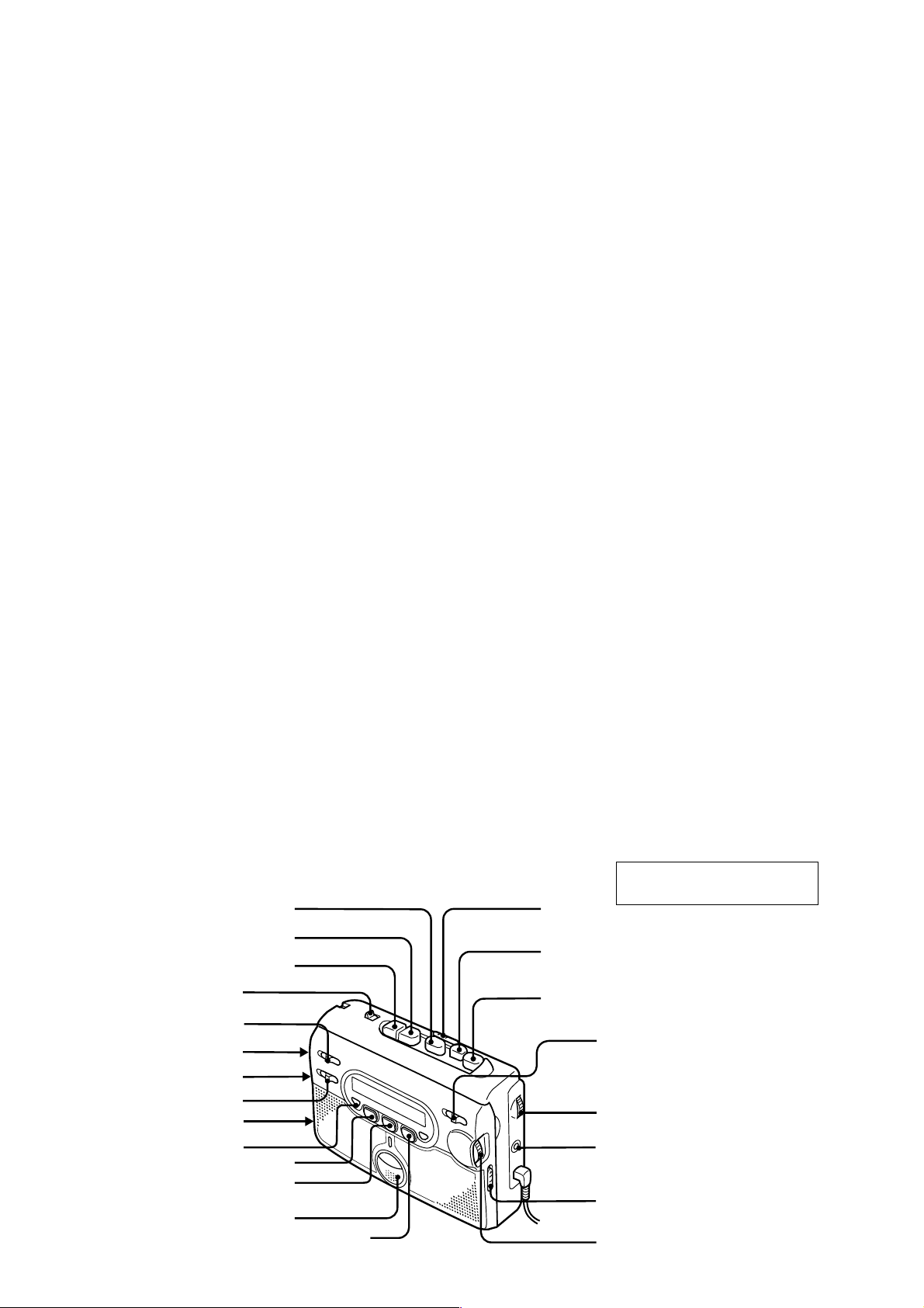
Location of parts and controls
Y PLAY
REW/REVIEW
FF/CUE
DIR
REC TIME
AVLS
ISS
SPEAKER
DC IN 3V
ENTER
built-in microphone
FM
AM
SECTION 1
GENERAL
OFF
5. EXPLODED VIEWS
5-1. Cabinet (Rear) Section .............................................. 20
5-2. Cassette Lid Section ................................................. 21
5-3. Mechanism Section-1 (MT-WMGX400-175) .......... 22
5-4. Mechanism Section-2 (MT-WMGX400-175) .......... 23
6. ELECTRICAL PARTS LIST ................................ 24
This section is extracted from
instruction manual.
PAUSE
x STOP
z REC
TUNING MODE
VOL
MIC (PLUG IN POWER)
i
FM MODE
FM MODE
TUNING
z
ST/MONO
(or/ou/oder)
z
DX/LOCAL
2
SECTION 2
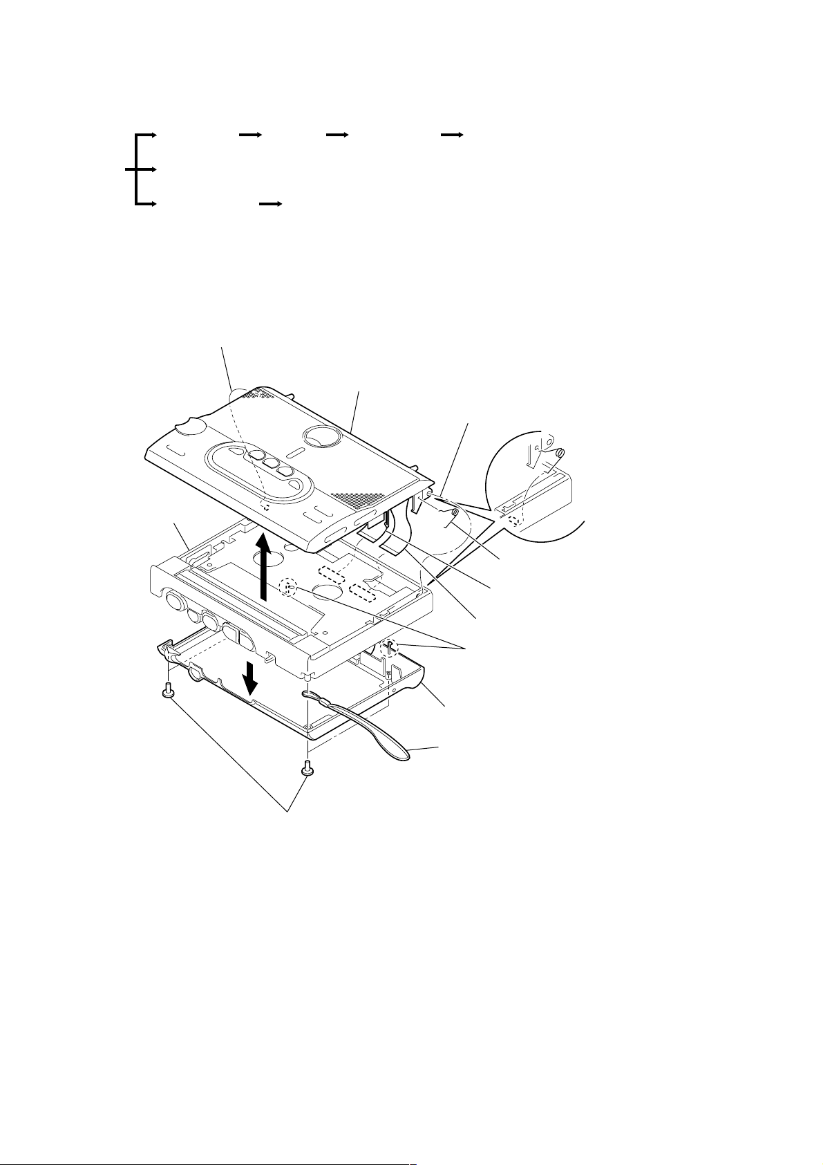
DISASSEMBLY
• The equipment can be removed using the following procedure.
WM-GX400
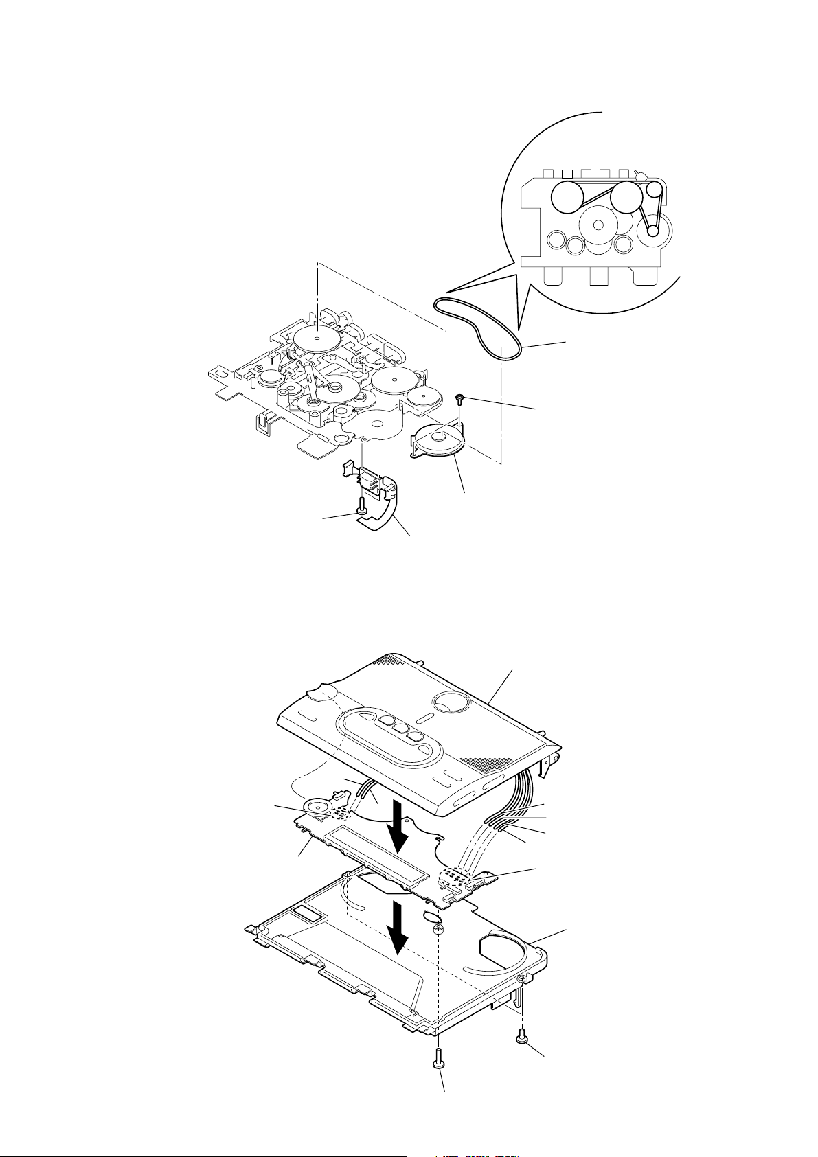
HRPE301 (REC/PB/ERASE head),
M601 (CAPSTAN/REEL motor), Belt (AR)
Set
Cabinet (Front) Main board
Cabinet (Rear)
Mechanism deck
Lid, cassette ASSY Display board
Note : Follow the disassembly procedure in the numerical order given.
2-1. CABINET (FRONT), CABINET (REAR), "LID, CASSETTE ASSY"
6 Remove from projection
Lid, cassette ASSY
6 Remove from projection
Cabinet (front)
Note on installing the
cassette lid assy
When installing the cassette lid ASSY,
insert the one side of the spring (toggle)
and set the other side into the gap on the
cabinet (front) as shown in the figure.
3
7
Spring (toggle)
4 Flexible board (22 core) (CN301)
5 Flexible board (22 core) (CN302)
2 Claws
Cabinet (rear)
Hand strap
1 Screws (+B1.7X9)
3
WM-GX400
)
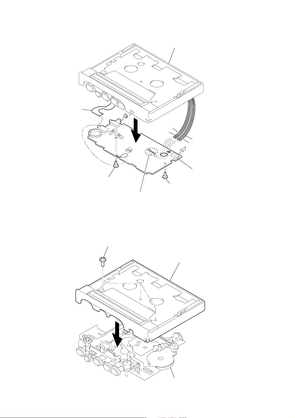
2-2. MAIN BOARD
2 Flexible board (9 core)
(CN303)
Cabinet (front)
2-3. MECHANISM DECK
3 Screw (M1.4)
1 Screws (IB LOCK)
4
1 Remove soldering
(four places)
White
Red
3 Screw (M1.4)
Black
Orange
Main board
Cabinet (front)
2
Mechanism deck (MT-WMGX400-175
4
)
2-4. HRPE301 (REC/PB/ERASE HEAD),
M601 (CAPSTAN/REEL MOTOR), BELT (AR)
WM-GX400
Attaching belt (AR)
3 Belt (AR)
4 Screws (M1.4)
1 Screws (M1.4)
2-5. DISPLAY BOARD
4 Remove soldering (from MIC301)
(two places)
Display board
Red
Black
5
5 M601 (CAPSTAN/REEL motor)
2 HRPE301 (REC/PB/ERASE head)
Lid, cassette ASSY
Gray
White
Brown
Orange
4 Remove soldering (from SP101, SP201
(four places)
3
1 Screw (+BTP1.7X5)
Holder, cassette
2 Screws (+BTP1.7)
5
WM-GX400
r
SECTION 3
ADJUSTMENTS
3-1. MECHANICAL ADJUSTMENTS
PRECAUTION
1. Clean the following parts with a denatured alcohol-moistened
swab :
record/playback/erase head pinch roller
capstan rubber belts
2. Demagnetize the record/playback/erase head with a head demag-
netizer. (Do not bring the head demagnetizer close to the erase
head.)
3. Do not use a magnetized screwdriver for the adjustments.
4. After the adjustments, apply suitable locking compound to the
parts adjusted.
5. The adjustments should be performed with the rated power sup-
ply voltage unless otherwise noted.
6. Power supply voltage : 3V DC.
Torque Measurement
Mode Torque Meter Meter Reading
1.97 to 3.92 mN • m
Forward/Reverse CQ-102C (20 to 40 g • cm)
(0.28 to 0.55 oz• inch)
Forward
Back Tension
Reverse
Back Tension
Fast Forward
and Rewind
CQ-102C (0.5 to 5.0 g • cm)
CQ-102RC (0.5 to 5.0 g • cm)
CQ-201B (50 g • cm)
0.05 to 0.49 mN • m
(0.007 to 0.07 oz• inch)
0.05 to 0.49 mN • m
(0.007 to 0.07 oz• inch)
more than 4.90 mN • m
(0.7 oz• inch)
3-2. ELECTRICAL ADJUSTMENTS
Note:
1. Supplied voltage: 3 V (DC)
2. Switch and control position
VOLUME control : maximum
SPEAKER/HEADPHONE switch : i (headphone)
AVLS switch : OFF
FUNCTION switch : OFF
ISS switch : 1
TAPE DECK SECTION 0 dB = 0.775 V
Test Tape
Type Signal Used for
WS-48A 3 kHz, 0 dB Tape Speed Adjustment
Tape Speed Adjustment
Procedure:
test tape
WS-48A
(3kHz, 0dB)
set
i headphone jack (J301)
1. Set REC TIME switch (S706) to NORMAL (4.8cm/s).
2. Play back the center portion of tape in REVmode, adjust RV602
so that the reading on the frequency counter becomes 3,000 Hz.
3. Set REC TIME switch (S706) to DOUBLE (2.4cm/s).
4. Play back the center portion of tape in REVmode, adjust RV601
so that the reading on the frequency counter becomes 1,500 Hz.
Specifications:
NORMAL (4.8cm/s) : 2,985Hz - 3,015Hz
DOUBLE (2.4cm/s) : 1,485Hz - 1,515Hz
5. Confirm the frequency difference between the beginning and
the end of tape should be 1.5%.
NORMAL (4.8cm/s) : 45Hz
DOUBLE (2.4cm/s) : 22.5Hz
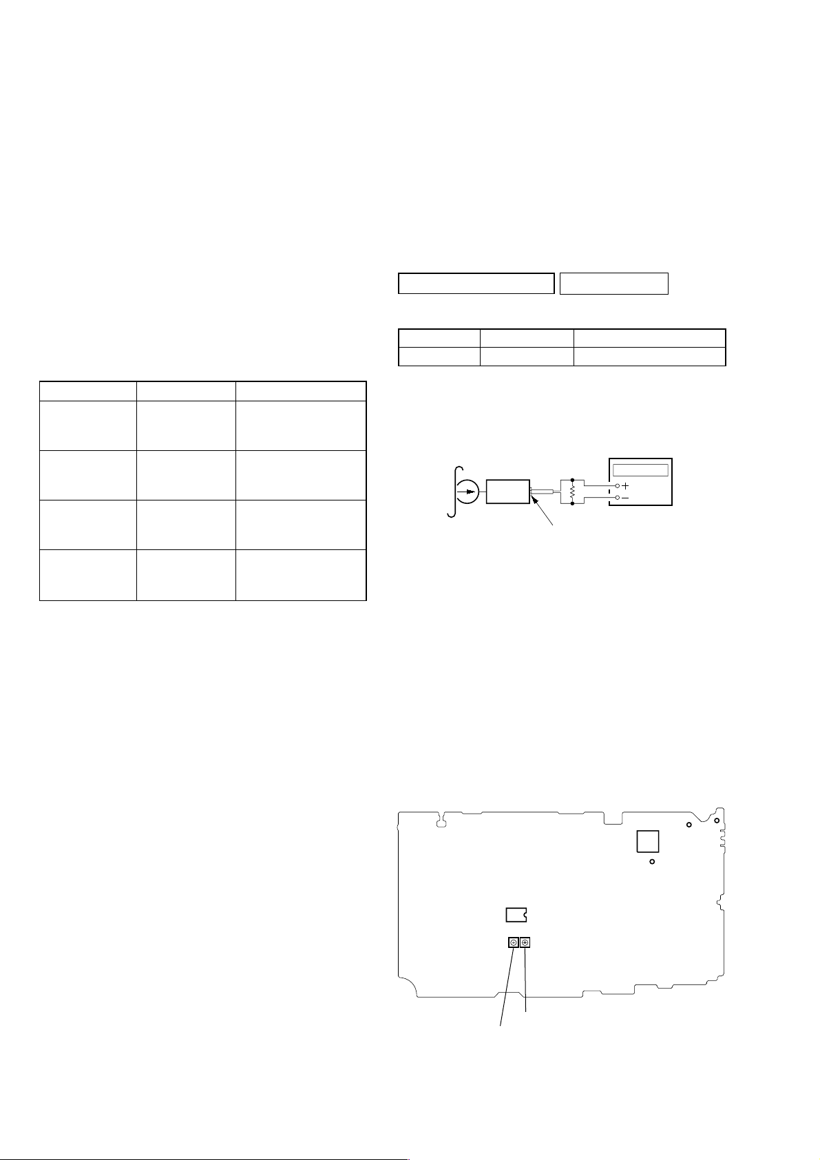
frequency counte
16Ω
Adjustment Location:
[MAIN BOARD] (SIDE B)
IC1
TP1
IC301
RV602
RV602: Tape Speed Adjustment (4.8cm/s)
RV601
RV601: Tape Speed Adjustment (2.4cm/s)
GND
TP2
6
SECTION 4
)
)
C
R11
DIAGRAMS
WM-GX400
TUNER SECTION 0 dB = 1 µV
AM Section
FUNCTION switch: AM
AM RF SSG
30% amplitude modulation by
400Hz signal.
Output level : as low as possible
FM Section
FUNCTION switch: FM
FM RF SSG
30% amplitude
modulation by
1kHz signal.
Deviation : ±75kHz
Output level : as low
• Repeat the procedures in each adjustment several times, and the
frequency coverage and tracking adjustments should be finally
done by the trimmer capacitors.
Adjust for a maximum reading on level meter.
RV2 999 kHz <1,000kHz>
Adjust for a maximum reading on level meter.
CT1 1,404 kHz <1,400kHz>
Adjust for a maximum reading on level meter.
Put the lead-wire
antenna close to
the set.
16
Ω
level meter
set
i
headphone jack (J301
level meter
Ω
0.01
µ
F
16
set
i
headphone jack (J301
main board
(side B)
TP2
as possible
no mark : 9kHz step
< > : 10kHz step
AM IF ADJUSTMENT
AM TRACKING ADJUSTMENT
L7 621 kHz <620kHz>
FM TRACKING ADJUSTMENT
L4 96.0 MHz
FM VCO Adjustment
Procedure:
[MAIN BOARD] (SIDE B)
FM RF SSG
C15
C28
D4
TP369
R15
TP2
FB201
TP368
FB101
FB301
C3
TP370
D2
3
47
0.01µF
Carrier frequency : 96MHz
Deviation : none
Output level : 562
µ
TP2
(ANT)
V (55dB)
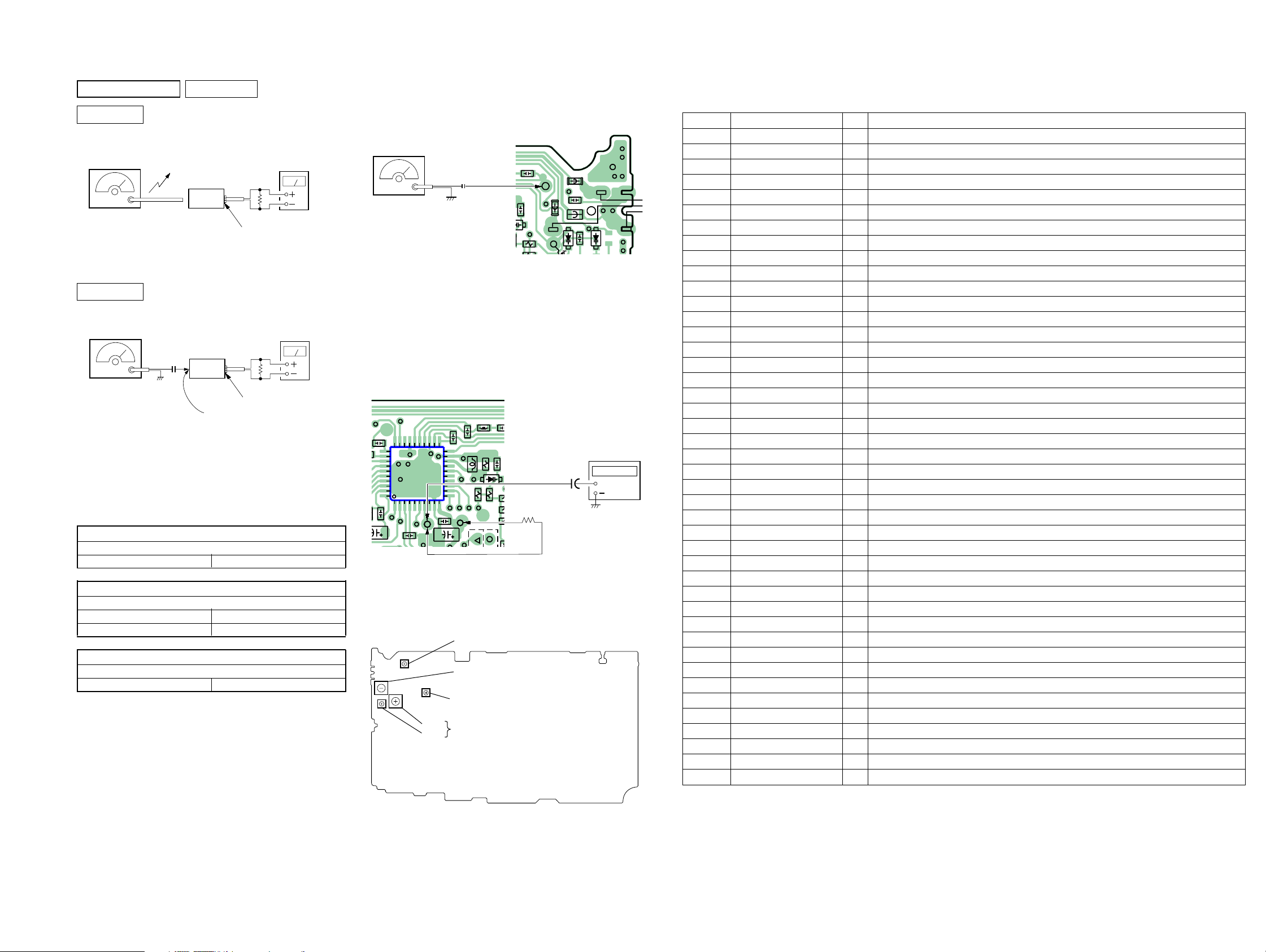
1. Connect the resistor 10kΩ between TP1 and TP332.
2. Connect the frequency counter to TP1 (IC1 7 pin).
3. Set FUNCTION switch to FM.
4. Tune the set in 96MHz.
5. Adjust RV1 so that the reading on the frequency counter becomes 76 kHz.
Specifications: 75 kHz - 77 kHz
[MAIN BOARD] (SIDE B)
C9
TP331
31
40
12
30
1
C8
C18
IC1
TP1
C21
C10
C1
L2
C20
21
20
L6
11
10
TP332
TP333
-4
R18
C28
R20
R17
C34
TP1
D
(IC1 7 pin)
10k
Ω
1
+
µ
F
frequency
counter
+
Adjustment Location:
[MAIN BOARD] (SIDE B)
RV2: AM IF Adjustment
L4: FM Tracking Adjustment
RV1: FM VCO Adjustment
L7:
AM Tracking Adjustment
CT1:
4-1. EXPLANATION OF IC TERMINALS
IC701 (SYSTEM CONTROL/LCD DRIVE) LC72349W-9A27
Pin No. Pin name I/O Description
1 XOUT O Connected to 75kHz Crystal oscillator
2 TEST2 I For Test
3 – 6 PA3 – 0 I Control key inputs
7 RADIO ON O Radio on/off control signal output
8, 9 PB2, 1 O Key source signal outputs
10 MOTOR BRK O Motor brake control signal output
11 PUSH I Tuning dial (S701) common switch signal input
12 PAUSE I Pause switch (S303) signal input
13 VERSION I Destination select signal input
14 BAND O Band select signal output
15 SD I SD input
16 COMP I COMP input
17 TU MODE I Tuning mode select switch (S707) signal input
18 TUNING-A I Tuning dial (S701) A switch signal input
19 AMP ON O Power amplifier on/off control signal output
20 BEEP O Beep signal output
21 BACK UP I Back-up voltage detection signal input
22 BATT I Battery voltage detection signal input
23 FACTORY — Not used Pull-up
24 VSS — Power supply ground terminal
25 MUTE O Mute signal output
26 MOTOR CTL O Motor control signal output
27 N/R SW O N/R switch signal output
28 REC I REC detection signal input
29 TAPE I Tape on/off detection signal input
30 X2 I Tape speed select switch (S706) signal input
31 TUNING-B I Tuning dial (S701) B switch signal input
32 PRE CTL — Not used
33 – 44 S12 – S1 O LCD driver segment output terminal
45 – 48 COM4 – 1 O LCD driver common output terminal
49 – 52 DBR4 – 1 I For LCD power supply booster
53 XRESET I System reset signal input
54 TU O Output for tuning voltage generator
55 VDD — Power supply terminal
56 FM IN I FM VCO input
57 AM IN I AM VCO input
58 VSS — Power supply ground terminal
59 E0 O Main charge pump output
60 AIN I LPF amplifier input
61 AOUT O LPF amplifier output
62 AGND — LPF amplifier ground
63 TEST1 I For test
64 XIN I Connected to 75kHz Crystal oscillator
77
WM-GX400
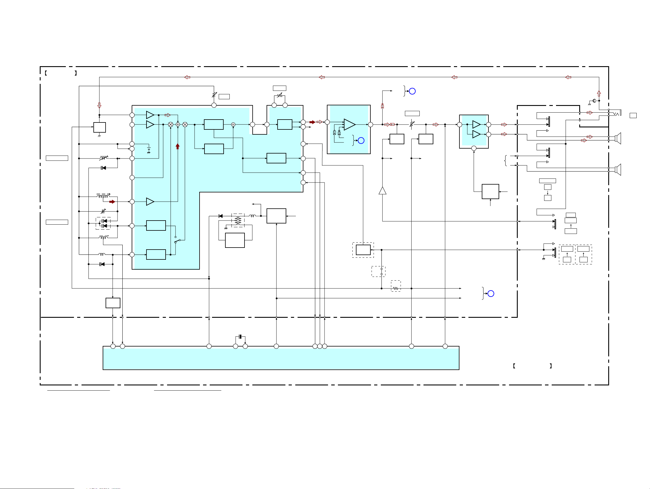
4-2. BLOCK DIAGRAMS – TAPE SECTION –
MIC301
Flat Mic
[DISPLAY BOARD] (1/3)
R-CH
S301-2
S301-1
MIC
VCC
S301-3
S301-4
R-CH
D406
ISS
SWITCH
Q335
S301
FWD
REV
VREF
VCC
REC
S302-2
S302-1
VREF
J302
MIC
(PLUG IN POWER)
HRPE301
REC/PB/ERASE HEAD
L
FWD
R
R
REV
L
FWD
REV
VCC
[MAIN BOARD] (1/2)
MIC
INPUT (L)
2
PB PRE
INPUT (L)
3
REC DRIVE
OUTPUT (L)
10
VREF
T331
S302
REC
PB
REFERENCE
1
BIAS
OSC
Q334,336
REC AMP
IC302
REC/PB AMP
MIC AMP
PRE AMP
REF
(1/2)
MIC
PR
REC DRIVE
INPUT (L)
PB/REC
SELECTOR
13
BATT
IC302
B
(2/2)
9
RV601
TAPE SPEED 2.4cm/S
RV602
TAPE SPEED 4.8cm/S
S303
PAUSE
ON
OFF
REC
SG
MAIN
BOARD
A
(2/2)
WAVE-
CURRENT
DETECT
17
OUT
-+
VSP
16
IN+
15
SPEED
DETECT
FORM
DETECT
MOTIVE
LOGIC
SOFT
SWITCH
PRE
DRIVE
MOTOR DRIVE/
SPEED CONTROL
U OUT
V OUT
W OUT
4
5
6
MOTOR
BRAKE
Q601-603
COM
U
V
W
M
CAPSTAN/REEL
M601
MOTOR
IC301
SPEED CONTROL
VREF
14
REF
BIAS
13
S/S
S601
(TAPE POWER)
[DISPLAY BOARD] (2/3)
VCC
S703
ISS
S706
TAPE SPEED
S707
TUNING MODE
3
2
1
MANUAL
PRESET
S708AMS709
FM
CRYSTAL
DISPLAY
ND701
LIQUID
S712
S710
OFF ENTER
BATT
17 26
TUN MODE MOTOR CTL
N/R SW
27
PB1
9
PB2
8
6
PA0
PA1
5
PA2
4
48
COM1
COM4
45
44
S1
S2
33
BATT
12 30
PAUSE X2
MOTOR BLK
SYSTEM
CONTROL
IC701
(1/2)
VERSION
TUNING-A
TUNING-B
AMP ON
TAPE
BATT
REC
PUSH
10
19
29
13
28
18
31
11
NORMAL
DOUBLE
BATT
DETECT
2 322
IC702
VDD
CBA
S701 (ROTALY)
TUNING
COM
BATT
MAIN
BOARD
(2/2)
VCC
SWITCH
MIC
VCC
RADIO ON
C
MUTE
Q356
GATE
Q354-355
REG
Q501, 502
BATT
DRY BATTERY
+
SIZE “AA”
(IEE DESIGNATION LR6)
2PCS, 3V
J501
DC IN 3V
R–CH IS OMITTED: SAME AS L–CH
• Signal path.
E : PB
a : REC
N : MIC
88
4-3. BLOCK DIAGRAMS – TUNER SECTION –
MAIN BOARD (2/2)
FRONT-END,
IF, DET, FM MPX
FM IN
25
TV IN
24
REGV
19
MREF
27
FMRO
22
TVRO
20
ARFI
26
AMLO
16
FTLO
18
AM
OSC
FM/TV
OSC
L4
FM TRACKING
L7, CT1
AM TRACKING
ATT
Q1
L4
D2
L3
AM FERRITE BAR
ANTENNA
CT1
D1
L7
L6
D4
BUFFER
Q3
IC1
FM/AM/TV
RV2
AM IF
29 2 1
IFCT
TUNER VCC
T401
DC-DC
CONVERTER
Q401
DFTO
35 36
L401
FM/TV LPF
FM DET.
AM BPF
AGC
LPF OUT
D402
MPRG
MPXI
TUNER B+
Q307, 308
RV1
FM VCO
LEVEL
DETECT
SWITCH
RADIO ON
VCO
MPX
LOUT
ROUT
PLT2
COMP
TUNE
BAND
VCC
3 7
4
R-CH
37
13
11
12
IC302
TUNER
INPUT (L)
PRE AMP
MIC
PB
REC
(2/2)
LINE
OUT (L)
8 6 3
B
IC302
(1/2)
SWITCH
Q2
EXCEPT CND, 5E
JC2
CND, 5E
SG
AVLS
Q405
R-CH
Q301, 302
R22
EXCEPT CND, 5E
A
RV301
VOLUME
MUTE
MAIN BOARD
(2/2)
MUTE
Q101
R-CH
IC101
IC201
BTL
POWER AMP
+
VCC
2
MUTE
RADIO ON
-
(L-CH)
(R-CH)
1
AMP B+
SWITCH
Q371-374
MIC VCC
C
R-CH
VCC
MAIN BOARD
(1/2)
WM-GX400
J301
i
SP101
SPEAKER
(L-CH)
SP201
SPEAKER
(R-CH)
S702
SPEAKER
OFF
ON
S702-1
S702-2
MONO
ST
EXCEPT
CND, 5E
S704
AVLS
NORM
LIMIT
S705
LOCAL
DX
CND, 5E
+
-
+
-
+
-
+
-
X701
75kHz
56 57 61 16 15 14 25 2071 64
FM IN
AM IN
R–CH IS OMITTED: SAME AS L–CH
SYSTEM CONTROL
IC701
(2/2)
AOUT
XOUT
XIN
RADIO ON
COMP
SD
BAND
MUTE
BEEP
DISPLAY BOARD (3/3)
• Signal path.
F : FM
f : AM
a : REC
E : PB
• Abbreviation
CND : Canadian
5E : Indication of country of origin (DX, LOCAL)
99
 Loading...