

Sony WMFX-451 Service manual
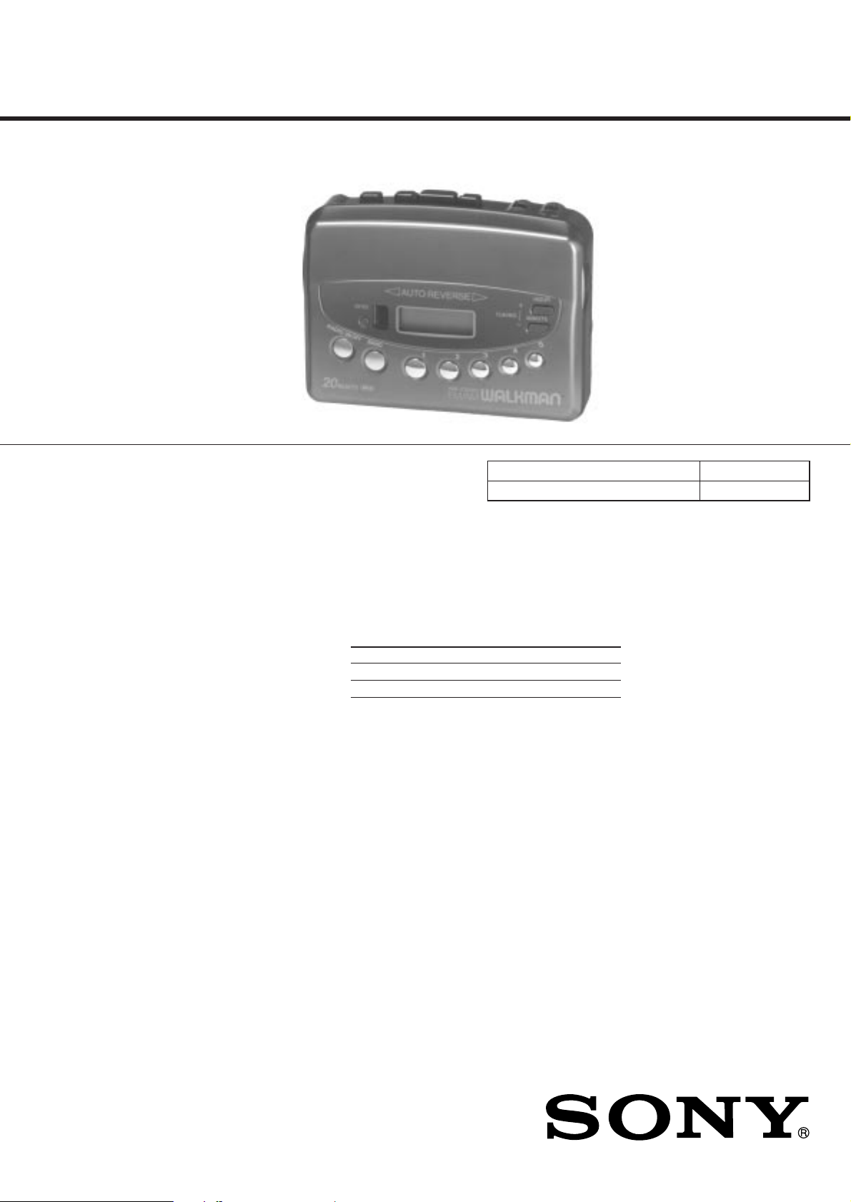
WM-FX451
SERVICE MANUAL
Ver 1.3 2004. 03
SPECIFICATIONS
Frequency range FM :
87.5 – 108 MHz
AM :
530 – 1710kHz (US, 7E model)
531 – 1602kHz (EXCEPT US, 7E model)
Battery life (Aprrox. hours)
Sony alkaline LR6 (SG) Sony R6P (SR)
playback 24 7.5
radio 33 13
Power requirements 3V DC batteries R6 (AA) x2/External DC 3V power sources
Dimensions 112.5x87.3x35.2 mm (4 1/2 x 31/2 x17/
projecting parts and controls
Mass Approx. 155g (5.5 oz)
Approx. 235g (8.3 oz) incl. batteries, a cassette and headphones
Supplied accesories Stereo headphones (1)/Belt clip (1)
US Model
AEP Model
E Model
Model Name Using Similar Machanism WM-FX453
T ape Tr ansport Mechanism Type MF-WMFX453-114
inches) (w/h/d) incl.
16
9-923-305-12
2004C02-1
© 2004.03
Design and specifications are subject to change without notice
RADIO CASSETTE PLAYER
Sony Corporation
Personal Audio Company
Published by Sony Engineering Corporation

TABLE OF CONTENTS
Specifications ........................................................................... 1
1. GENERAL
Location of parts and controls............................................ 3
2. DISASSEMBLY
2-1. Cabinet (Rear) Sub Assy Removal ............................. 4
2-2. Main Board Removal ................................................. 5
2-3. Mechanism Deck Removal......................................... 5
2-4. Holder, Cassette Assy Removal.................................. 6
2-5. Display Board Removal ............................................. 6
3. ADJUSTMENTS
3-1. Mechanical Adjustments ............................................ 7
3-2. Electrical Adjustments................................................ 7
4. DIAGRAMS
4-1. Explanation of IC Terminals..................................... 10
4-2. Block Diagram...........................................................11
4-3. Printed Wiring Boards .............................................. 13
4-4. Schematic Diagram................................................... 17
5. EXPLODED VIEWS
5-1. Cabinet Section......................................................... 23
5-2. Mechanism Section (MF-WMFX453-114) .............. 24
6. ELECTRICAL PAR TS LIST................................... 25
Flexible Circuit Board Repairing
• Keep the temperature of the soldering iron around 270°C during
repairing.
• Do not touch the soldering iron on the same conductor of the
circuit board (within 3 times).
• Be careful not to apply force on the conductor when soldering or
unsoldering.
Notes on chip component replacement
• Never reuse a disconnected chip component.
• Notice that the minus side of a tantalum capacitor may be damaged by heat.
• HOW TO CHANGED THE CERAMIC FILTERS
This model is used two ceramic filters of CF2 and X2.
You must used same type of color marked ceramic filters in
order to meet same specifications.
Therefore, the ceramic filter must changed two pieces together
since it’s supply two pieces in one package as a spare parts
mark
CF2
mark
X2
Mark Center Frequency
red 10.70MHz
blue 10.67MHz
orange 10.73MHz
black 10.64MHz
white 10.76MHz
– 2 –
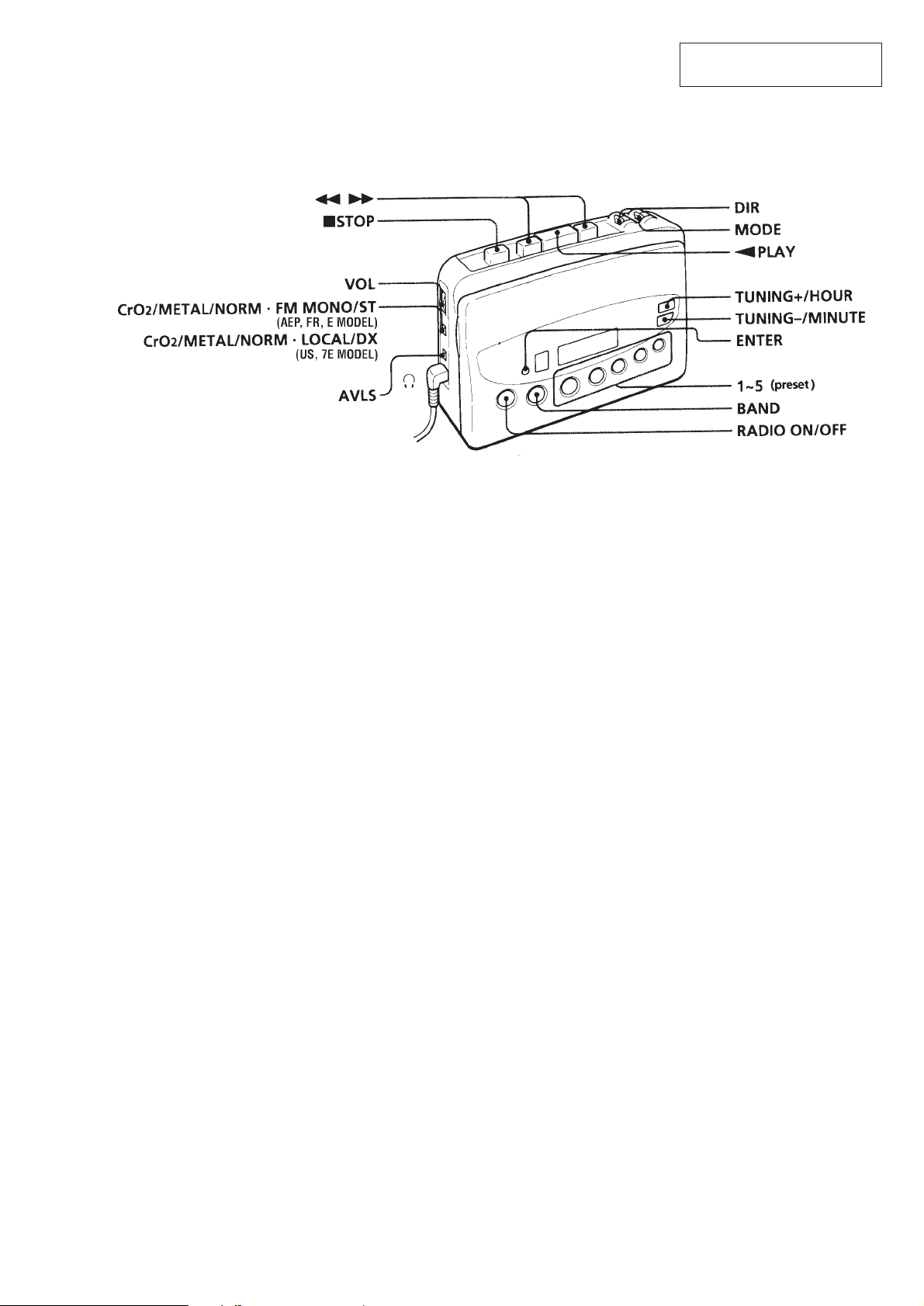
LOCATION OF PARTS AND CONTROLS
SECTION 1
GENERAL
This section is extracted from
instruction manual.
• Abbreviation
FR : French
E : Radio section : FM MONO/ST switch
7E : Radio section : DX/LOCAL switch
– 3 –
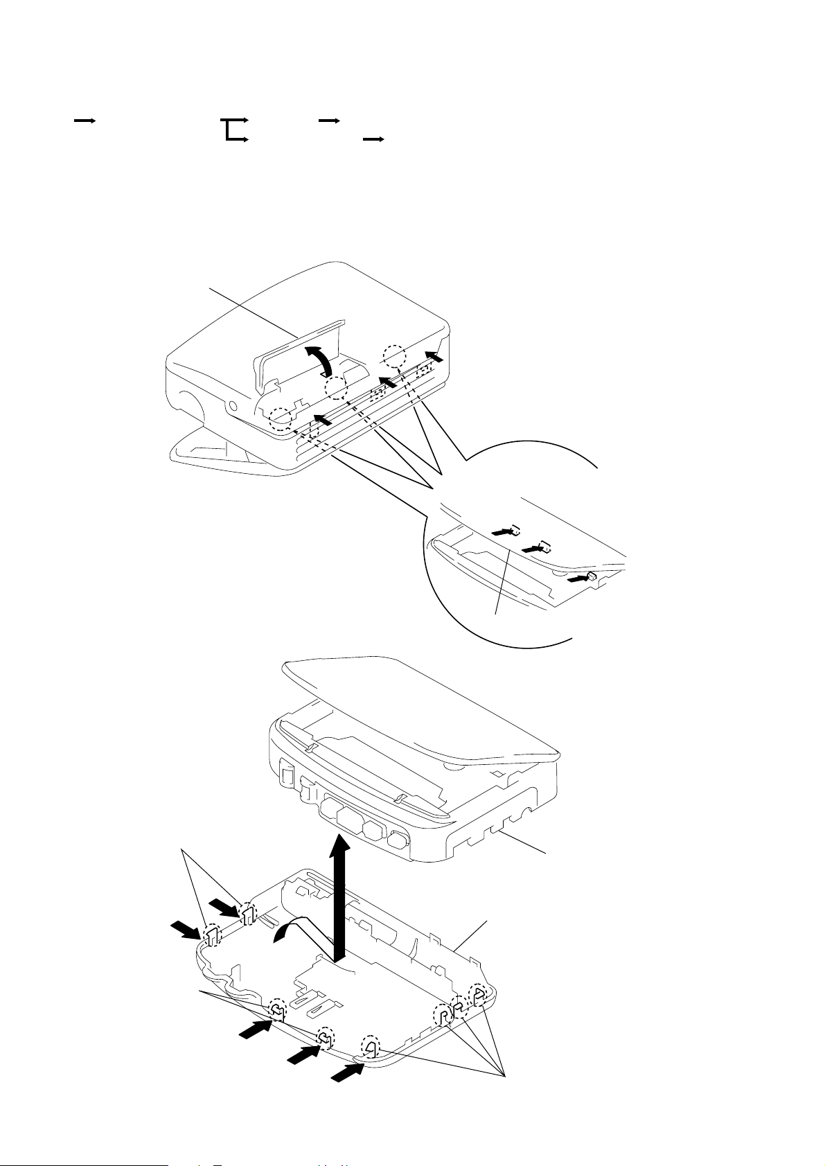
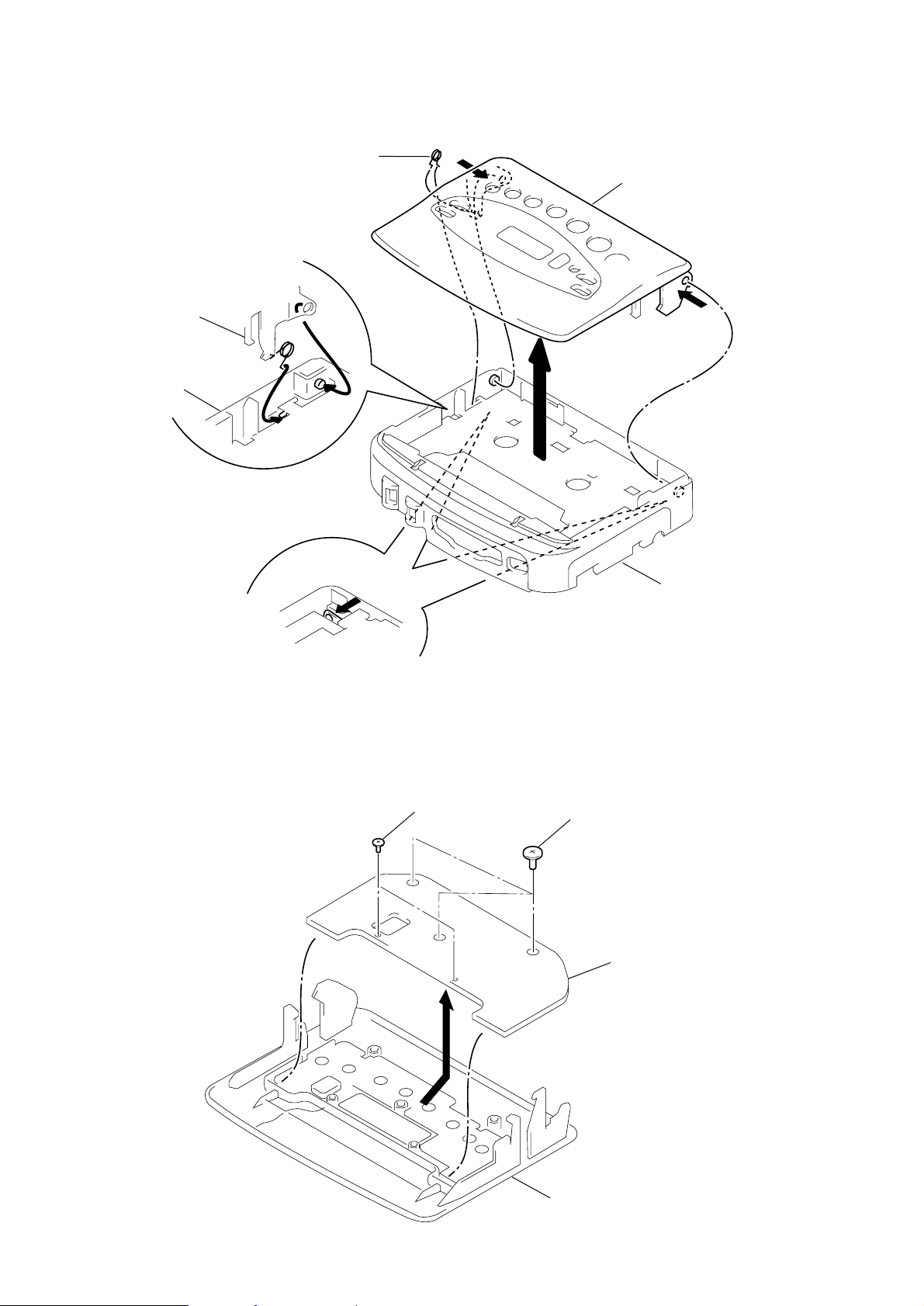
DISASSEMBLY
y
y
r
The equipment can be removed using the following procedure.
Set
Note : Follow the disassembly procedure in the numerical order given.
2-1. CABINET (REAR) SUB ASSY REMOVAL
Lid, Batt
Main boardCabinet (rear) sub assy
Holder, cassette ass
SECTION 2
Mechanism deck
Display board
1
6
4
2
3
5
7
Holder, Cassette
Claws
9
Claws
8
!º
!¡
!£
Cabinet, Front ass
Cabinet (Rear) sub assy
!™
Claws
– 4 –
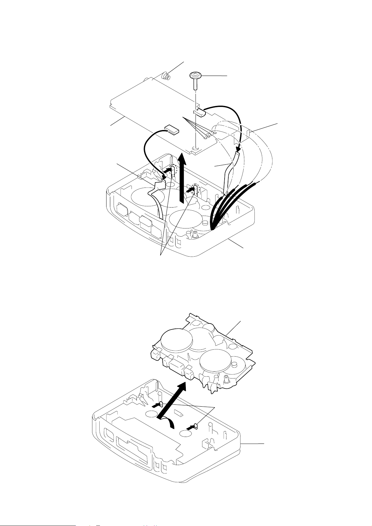
2-2. MAIN BOARD REMOVAL
t
y
Main board
2
Remove solder
3
Terminal (–), Batt
1
Screw (M1.4), Tooth (WH)
4
Terminal (+), Bat
Flexible board for head
2-3. MECHANISM DECK REMOVAL
Claws
5
7
FPC1
6
Cabinet, Front assy
Mechanism deck
1
3
Claws
2
Cabinet, Front ass
– 5 –
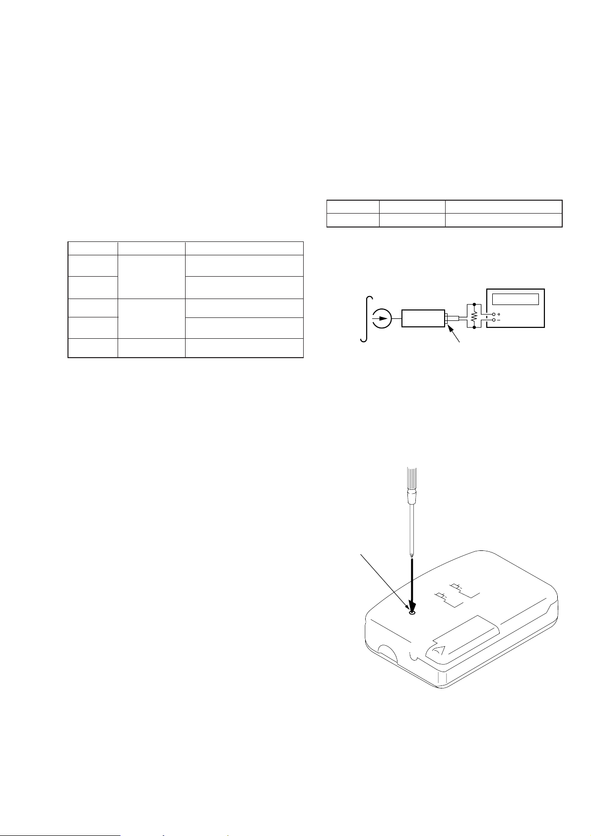
2-4. HOLDER, CASSETTE ASSY REMOVAL
3
Spring (Lid up)
• Use caution when installing the
holder, cassette assy
Install the holder , cassette with the spring (lid up)
as shown in A in the drawing so that it fits into the
holes on the cabinet fr ont assy . Once installed,
fit the left and right pieces on.
Holder, Cassette assy
Holder, Cassette assy
Cabinet front assy
2-5. DISPLAY BOARD REMOVAL
A
1
• Press on the left & right clips from the rear of the
cabinet fr ont assy . and remo ve the boss.
1
Screws
2
2
Cabinet, Front assy
Screws
3
– 6 –
Display board
Holder, Cassette assy
SECTION 3
RV601
r
ADJUSTMENTS
3-1. MECHANICAL ADJUSTMENTS
PRECAUTION
1. Clean the following parts with a denatured-alcohol-moistened
swab :
playback head pinch roller
capstan rubber belt
2. Dema gnetiz e the pla ybac k head with a head dema gnetiz er.
3. Do not use a magnetized screwdriver for the adjustments.
4. After the adjustments, apply suitable locking compound to the
parts adjusted.
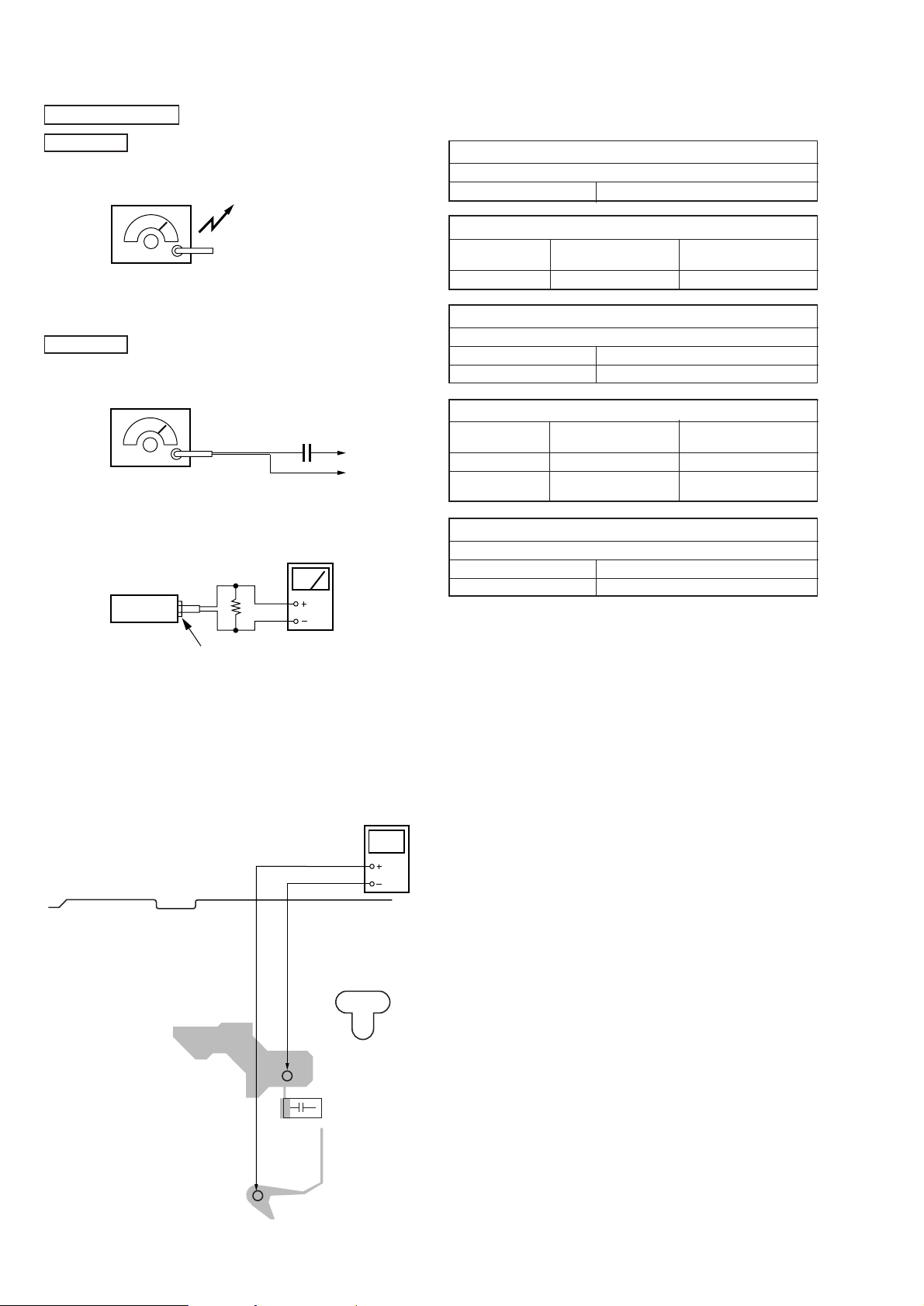
5. The adjustments should be performed with the rated power supply volta ge (2.5 V) unless otherwise noted.
Torque Measurement
Mode Torque Meter Meter Reading
FWD
FWD less than 2 g • cm
back tension (less than 0.03 oz• inch)
REV
REV less than 2 g • cm
back tension (less than 0.03 oz• inch)
FF, REW CQ-201B
CQ-102C
CQ-102RC
20 - 42 g • cm
(0.28 -0.58 oz• inch)
20 - 42 g • cm
(0.28 -0.58 oz• inch)
more than 60 g • cm
(more than 0.83 oz• inch)
3-2. ELECTRICAL ADJUSTMENTS
PRECAUTION
• Supplied v olta ge : 2.5V.
• Switch and control position
T APE s witc h : NORM
MODE switch : d
VOLUME control : maximum
A VLS s witc h : NORM
Test T ape
Type Signal Used for
WS-48A 3kHz, 0dB Tape Speed Adjustment
Tape Speed Adjustment
Procedure :
test tape
WS-48A
(3kHz, 0dB)
set
frequency counte
16
Ω
phones jack
1. Pla ybac k WS-48A (tape center par t) in the REV state and adjust
RV601 so that the frequenc y counter reading becomes 3,000Hz
± 15Hz.
2. Pla ybac k WS-48A (tape center) in the FWD state .
Check that frequency counter reading is within 1.5% of the reading of step 1.
Adjustment Location :
– 7 –
TUNER SECTION
)
r
r
AM Section
BAND : AM
AM RF signal
generator
30% amplitude modulation by 400Hz
signal.
Output level : as low as possible
FM Section
BAND : FM
FM RF signal
generator
22.5kHz frequency deviation by
400Hz signal.
Output level : as low as possible
set
Put the lead-wire
antenna close to
the set.
Ω
16
J301 (phones)
µ
F
0.01
level mete
(ANT TAP
(GND)
no mark : US, 7E model
< > : EXCEPT US, 7E model
AM IF ALIGNMENT
Adjust for a maximum reading on level meter.
T1 1000kHz < 999kHz>
AM FREQUENCY COVERAGE ADJUSTMENT
Adjust part Frequency display
L4 530kHz < 531kHz> 1.4 ± 0.1V< 1.4 ± 0.1V>
AM TRACKING ADJUSTMENT
Adjust for a maximum reading on level meter.
L1 620kHz < 621kHz>
CT1 1,400kHz< 1,395kHz>
FM FREQUENCY COVERAGE ADJUSTMENT
Adjust part Frequency display
L3 87.5MHz< 87.5MHz> 2.4 ± 0.1V< 2.4 ± 0.1V>
Confirmation 108MHz <108MHz>
FM TRACKING ADJUSTMENT
Adjust for a maximum reading on level meter.
L2 87.5MHz <87.5MHz>
Confirmation 108MHz <108MHz>
reading on digital
voltmeter.
reading on digital
voltmeter.
less than 10V
<less than 10V>
• Abbreviation
7E : Radio section : DX/LOCAL switch
* Repeat the procedures in each adjustment several times, and the
frequency coverage and tracking adjustments should be finally
done by the trimmer capacitors.
Frequency Coverage Adjustment
Setting :
(VT)
[MAIN BOARD] (Side B)
(GND)
GND
digital voltmete
(DC range)
C21
VT
– 8 –
t
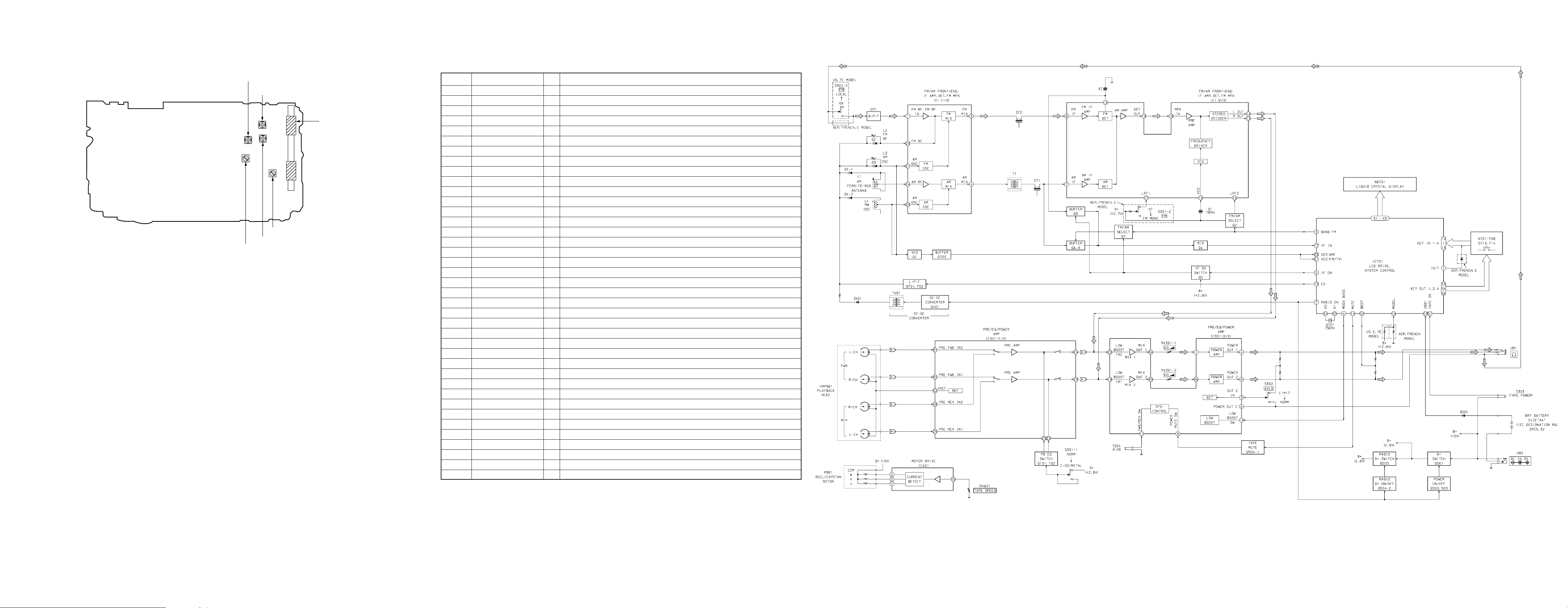
SECTION 4
DIAGRAMS
WM-FX451
Adjustment Location :
[MAIN BOARD] (Side A)
L4 : AM Frequency Coverage Adjustment
CT1 : AM Tracking Adjustment
L1 : AM Tracking Adjustmen
L2 : FM Tracking Adjustment
T1 : AM IF Alignment
L3 : FM Frequency Coverage Adjustment
4-1. EXPLANATION OF IC TERMINALS
IC701 µ PD17072GB-540-1A7 (LCD DRIVE, SYSTEM CONTROL)
Pin No. Pin name I/O Description
1 INIT I Key initial terminal.
2 BAND AM O BAND AM ON selection output.
3 BAND FM O BAND FM ON selection output.
4 MEGA BASS I MEGA BASS ON/OFF input (Not used).
5 IF ON O IF ON/OFF control.
6 – Not used (Open).
7 RADIO ON O Radio power ON/OFF control.
8 – Not used (Open).
9 – Not used (Open).
10 KEY IN 1 I Key input.
11 KEY IN 2 I Key input.
12 KEY IN 3 I Key input.
13 KEY IN 4 I Key input.
14 MUTE O Mute signal output.
15 DOLBY O Dolby ON/OFF control (Not used).
16 MODEL I Model select terminal.
17 IF IN I IF signal input.
18 GND – Ground.
19 EO O PLL error output.
20 VCO (AM) I VCO input.
21 VCO (FM/TV) I VCO input.
22 VDD2 – Power supply terminal (+3V).
23 VDD1 – Power supply terminal (+3V).
24 X0 O System clock oscillator (75kHz).
25 X1 I System clock oscillator (75kHz).
26 VDD5 – Power supply (+3V).
27 VDD3 – Power supply (+3V).
28 CAP 1 – Pins connecting capacitors for doubler circuits gemerating the ND drive voltage.
29 CAP 2 – Pins connecting capacitors for doubler circuits gemerating the ND drive voltage.
30 VDD4 – Power supply (+3V).
31 – 34 COM 0 – 3 O ND common output.
35 – 49 LCD 0 – 14 O ND segment drive output.
50 CE I The internal reset circuit functions when low becomes high.
51 TAPE ON I TAPE ON signal input.
52 BEEP O BEEP signal output.
53 KEY OUT 1 O Key scan output.
54 KEY OUT 2 O Key scan output.
55 KEY OUT 3 O Key scan output.
56 KEY OUT 4 O Key scan output.
4-2. BLOCK DIAGRAM
– 9 – – 10 – – 12 –– 11 –
• Signal path.
F :FM
E :PB
• Abbreviation
FR : French
E : Radio section : FM MONO/ST switch
7E : Radio section : DX/LOCAL switch
 Loading...