

Sony TRINITRON KV-34DRC430, TRINITRON KV-36DRC430 Service Manual

HISTORY INFORMATION FOR THE FOLLOWING MANUAL:
SERVICE MANUAL
MODEL NAME REMOTE COMMANDER DESTINATION CHASSIS NO.
KV-34DRC430
KV-34DRC430
KV-36DRC430
KV-36DRC430
RM-Y197 LATIN NORTH SCC-S71N-A
RM-Y197 LATIN SOUTH SCC-S71P-A
RM-Y197 LATIN NORTH SCC-S71Q-A
RM-Y197 LATIN SOUTH SCC-S71R-A
DA-4
CHASSIS
ORIGINAL MANUAL ISSUE DATE: 3/2005
REVISION DATE SUBJECT
3/2005 No revisions or updates are applicable at this time.
9-965-978-01
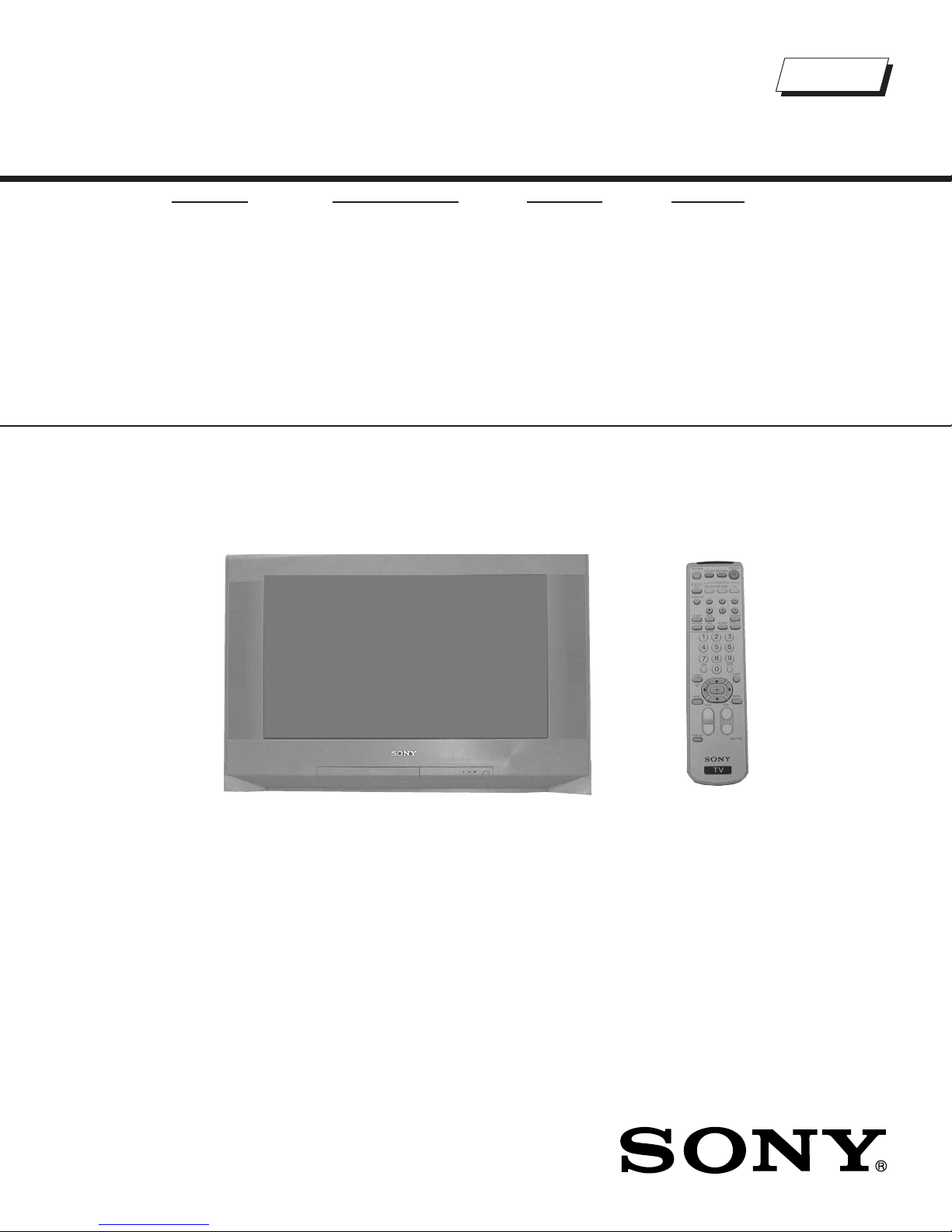
TRINITRON® COLOR TELEVISION
Self Diagnosis
Supported model
SERVICE MANUAL
MODEL NAME REMOTE COMMANDER DESTINATION CHASSIS NO.
KV-34DRC430
KV-34DRC430
KV-36DRC430
KV-36DRC430
RM-Y197 LATIN NORTH SCC-S71N-A
RM-Y197 LATIN SOUTH SCC-S71P-A
RM-Y197 LATIN NORTH SCC-S71Q-A
RM-Y197 LATIN SOUTH SCC-S71R-A
DA-4
CHASSIS
9-965-978-01
RM-Y197
KV-36DRC430
TRINITRON® COLOR TELEVISION

KV-34DRC430/36DRC430
TABLE OF CONTENTS
SECTION TITLE PAGE SECTION TITLE PAGE
Specifi cations ................................................................................. 4
Warnings and Cautions .................................................................. 6
Safety Check-Out ........................................................................... 7
Self-Diagnostic Function ................................................................. 8
SECTION 1: DISASSEMBLY ................................................................11
1-1. Rear Cover Removal .............................................................11
1-2. Chassis Assembly Removal ..................................................11
1-3. Service Position .................................................................... 11
1-4. Picture Tube Removal .......................................................... 12
Anode Cap Removal Procedure .......................................... 12
Cable Wire Dressing ............................................................ 13
SECTION 2: SET-UP ADJUSTMENTS ................................................ 20
2-1. Beam Landing ...................................................................... 20
2-2. Convergence ........................................................................ 21
2-2.1. Vertical and Horizontal Static Convergence ............ 21
2-3. V-PIN and V-CEN Adjustment .............................................. 21
2-3.1. Operation of BMC (Hexapole) Magnet .................... 21
2-3.2. TLH Plate Adjustment .............................................. 22
2-3.3. Screen-Corner Convergence ................................... 22
2-3.4. Dynamic Convergence Adjustments ........................ 22
2-4. Focus Adjustment ................................................................. 23
2-4.1. Dynamic Focus/Dynamic Quadra-Pole Data ........... 23
2-5. Screen(G2) ........................................................................... 24
2-6. Picture Quality Adjustments ................................................. 24
2-6.1. Video Input - Sub Contrast Adjustment .................... 24
2-6.2. Video Input - Sub Hue/Sub Color Adjustment .......... 25
2-6.3. RF Input - Sub Contrast Adjustment ........................ 25
2-6.4. RF Input - Sub Hue/Sub Color Adjustment .............. 26
2-7. White Balance (CRT) and Sub Bright Adjustment ................ 26
2-7.1. Color Offset Adjustment Procedure ......................... 26
2-8. H Raster Center Adjustment ................................................ 27
2-9. Picture Distortion Adjustments ............................................. 27
2-9.1. NTSC (DRC) Full Mode Adjustment ........................ 27
2-9.2. 1080i HD Mode Adjustment ..................................... 28
2-9.3. Vertical Compressed Mode Check and Confi rmation
(For 4x3 CRT Only) ................................................. 28
2-9.4 Normal, Zoom and Wide Zoom Modes .................... 28
SECTION 3: SAFETY RELATED ADJUSTMENTS ............................. 29
3-1. Preparation Before Confi rmation .......................................... 29
3-1.1 Hold-Down Operation Confi rmation ......................... 29
3-2. B+ Max Confi rmation ........................................................... 29
3-3. B+ Voltage Check ................................................................ 29
3-4. High Voltage (HV) Check) .................................................... 29
3-5. Preparation for HV and IK Protector Check ......................... 29
3-6. HV Protector Check ............................................................. 29
3-6-1. Cut Off Condition ..................................................... 29
3-6-2. High Light Condition ................................................ 30
3-7. IK Protector Check ............................................................... 30
3-8. Hold Down Check ................................................................ 30
3-9. Restoration ........................................................................... 30
3-10. HV Service Flowchart ........................................................... 31
HV Service Flowchart Table ................................................. 32
KV-34DRC430/36DRC430
SECTION 4: CIRCUIT ADJUSTMENTS .............................................. 33
4-1. Setting Service Adjustment Mode ........................................ 33
4-1.1. Service Adjustment Mode In .................................... 33
4-1.2. Service Adjustment Mode Memory .......................... 33
4-1.3. Reading the Memory ............................................... 33
4-1.4. Adjusting the Picture ................................................ 33
4-1.5. Resetting the Data ................................................... 33
4-1.6. Resetting the MID NVM Data .................................. 33
4-1.7. Resetting the System NVM Data ............................. 33
4-1.8. Copy Function .......................................................... 33
4-2. Memory Write Confi rmation Method .................................... 34
4-3. Remote Adjustment Buttons and Indicators ......................... 34
4-4. Service Data ......................................................................... 35
4-5. ID Map Table ........................................................................ 58
SECTION 5: DIAGRAMS ..................................................................... 59
5-1. Circuit Boards Location ........................................................ 59
5-2. Printed Wiring Boards and
Schematic Diagrams Information ......................................... 59
5-3. Block Diagrams .................................................................... 60
5-4. Schematics and Supporting Information .............................. 63
DZ Board Schematic Diagram (1 of 2) ................................. 63
DZ Board Schematic Diagram (2 of 2) ................................. 64
UY Board Schematic Diagram ............................................. 67
HBY Board Schematic Diagram ........................................... 68
AY Board Schematic Diagram (1 of 2) ................................. 71
AY Board Schematic Diagram (2 of 2) ................................. 72
HCX Board Schematic Diagram .......................................... 75
CH Board Schematic Diagram ............................................. 77
HAX Board Schematic Diagram .......................................... 79
WY Board Schematic Diagram ............................................ 80
MY Board Schematic Diagram (1 of 4) ................................ 82
MY Board Schematic Diagram (2 of 4) ................................ 83
MY Board Schematic Diagram (3 of 4) ................................ 84
MY Board Schematic Diagram (4 of 4) ................................ 85
BY Board Schematic Diagram (1 of 4) ................................. 88
BY Board Schematic Diagram (2 of 4) ................................. 89
BY Board Schematic Diagram (3 of 4) ................................. 90
BY Board Schematic Diagram (4 of 4) ................................. 91
P Board Schematic Diagram ............................................... 92
PA Board Schematic Diagram ............................................. 93
5-5. Semiconductors (1 of 2) ....................................................... 94
Semiconductors (2 of 2) ....................................................... 95
SECTION 6: EXPLODED VIEWS ........................................................ 96
6-1.Chassis .................................................................................. 96
6-2. Picture Tube ........................................................................ 97
SECTION 7: ELECTRICAL PARTS LIST ........................................... 98
3
SPECIFICATIONS
KV-34DRC430/36DRC430
KV-34DRC430
LATIN NORTH
KV-34DRC430
LATIN SOUTH
KV-36DRC430
LATIN NORTH
KV-36DRC430
LATIN SOUTH
Power Requirements 120V, 60Hz 220V, 60Hz 120V, 60Hz 220V, 60Hz
Number of Inputs/Outputs
Audio Out
Video
S Video
Y,PB, PR
Audio
1)
2)
3)
4)
5)
4444
3333
2222
7777
1111
Monitor Out 1111
Control-S (In/Out) YES YES YES YES
Memory Stick NO NO NO NO
Power Consumption (W)
Speaker Output (W)
10w x 2 10w x 2 10w x 2 10w x 2 15W
In Use (Max) 240W 240W 240W 240W
In Standby 1W 1W 1W 1W
Dimensions (W x H x D)
mm 898 x 698 x 598 mm 898 x 698 x 598 mm 994 x 654 x 606 mm 994 x 654 x 606 mm
3/8
1/2
1/2
3/8
1/2
1/2
1/8
3/4
3/4
1/8
35
x 27
x 23
in 35
x 27
x 23
in 39
x 25
x 23
in
in 39
x 25
3/4
x 23
Mass
kg 74.8 kg 74.8 kg 88 kg 88 kg
lbs 165 lbs 165 lbs 230 lbs 230 lbs
1) 1 Vp-p 75 ohms unbalanced, sync negative
2) Y: 1 Vp-p 75 ohms unbalanced, sync negative
C: 0.286 Vp-p (Burst signal), 75 ohms
3) Y: 1.0 Vp-p, 75 ohms unbalanced, sync negative;
PB: 0.7 Vp-p, 75 ohms
PR: 0.7 Vp-p, 75 ohms
4) 500 mVrms (100% modulation), Impedance: 47 kilohms
5) More than 408 mVrms at the maximum volume setting (variable)
More than 408 mVrms (fi x); Impedance (output): 2 kilohms
3/4
in
TruSurround
by SRS
™
®
TruSurround is a trademark of SRS Labs, Inc. SRS and the SRS
symbol are registered trademarks of SRS Labs, Inc. in the United
States and in select foreign countries. SRS and TruSurround are
incorporated under license from SRS Labs, Inc. and are protected
under United States Patent Nos. 4,748,669 and 4,841,572 with
numerous additional issued and pending foreign patents. Purchase of this product does not convey the right to sell recordings
made with the TruSurround technology.
KV-34DRC430/36DRC430
SRS (SOUND RETRIEVAL SYSTEM)
The SRS (SOUND RETRIEVAL SYSTEM) is manufactured
by Sony Corporation under license from SRS Labs, Inc. It is
covered by U.S. Patent No. 4,748,669. Other U.S. and foreign
patents pending.
The word ‘SRS’ and the SRS symbol
are registered trademarks of SRS Labs, Inc. BBE and BBE symbol are trademarks of
BBE Sound, Inc. and are licensed by BBE Sound, Inc. under U.S.
Patent No. 4,638,258 and 4,482,866.
Design and specifi cations are subject to change without notice.
4

Television system
American TV standard, NTSC
Channel coverage
VHF: 2-13/ UHF: 14-69/ CATV: 1-125
Picture tube
FD Trinitron® tube
Visible screen size
32-inch picture measured diagonally (KV-34DRC430 Only)
34-inch picture measured diagonally (KV-36DRC430 Only)
Actual screen size
34-inch measured diagonally (KV-34DRC430 Only)
36-inch measured diagonally (KV-36DRC430 Only)
Antenna
75 ohm external terminal for VHF/UHF
Supplied Accessories
Remote Commander RM-Y197
Two Size AA (R6) Batteries
KV-34DRC430/36DRC430
Optional Accessories
AV Cable: VMC-810/820/830 HG
Audio Cable: RKC-515HG
Component Video Cable: VMC-10/30 HG
TV Stand: SU-34HX1 (KV-34DRC430 Only)
TV Stand: SU-36HX1 (KV-36DRC430 Only)
KV-34DRC430/36DRC430
5
KV-34DRC430/36DRC430
WARNINGS AND CAUTIONS
CAUTION
Short circuit the anode of the picture tube and the anode cap to the metal chassis, CRT shield, or carbon painted on the CRT, after
removing the anode.
WARNING!!
An isolation transformer should be used during any service to avoid possible shock hazard, because of live chassis. The chassis of
this receiver is directly connected to the ac power line.
!
SAFETY-RELATED COMPONENT WARNING!!
Components identifi ed by shading and ! mark on the schematic diagrams, exploded views, and in the parts list are critical for
safe operation. Replace these components with Sony parts whose part numbers appear as shown in this manual or in supplements
published by Sony. Circuit adjustments that are critical for safe operation are identifi ed in this manual. Follow these procedures
whenever critical components are replaced or improper operation is suspected.
KV-34DRC430/36DRC430
6
SAFETY CHECK-OUT
g
KV-34DRC430/36DRC430
After correcting the original service problem, perform the following
safety checks before releasing the set to the customer:
1. Check the area of your repair for unsoldered or poorly soldered
connections. Check the entire board surface for solder splashes and
bridges.
2. Check the interboard wiring to ensure that no wires are “pinched” or
touching high-wattage resistors.
3. Check that all control knobs, shields, covers, ground straps, and
mounting hardware have been replaced. Be absolutely certain that
you have replaced all the insulators.
4. Look for unauthorized replacement parts, particularly transistors,
that were installed during a previous repair. Point them out to the
customer and recommend their replacement.
5. Look for parts which, though functioning, show obvious signs of
deterioration. Point them out to the customer and recommend their
replacement.
6. Check the line cords for cracks and abrasion. Recommend the
replacement of any such line cord to the customer.
7. Check the B+ and HV to see if they are specifi ed values. Make sure
your instruments are accurate; be suspicious of your HV meter if
sets always have low HV.
8. Check the antenna terminals, metal trim, “metallized” knobs, screws,
and all other exposed metal parts for AC leakage. Check leakage as
described below.
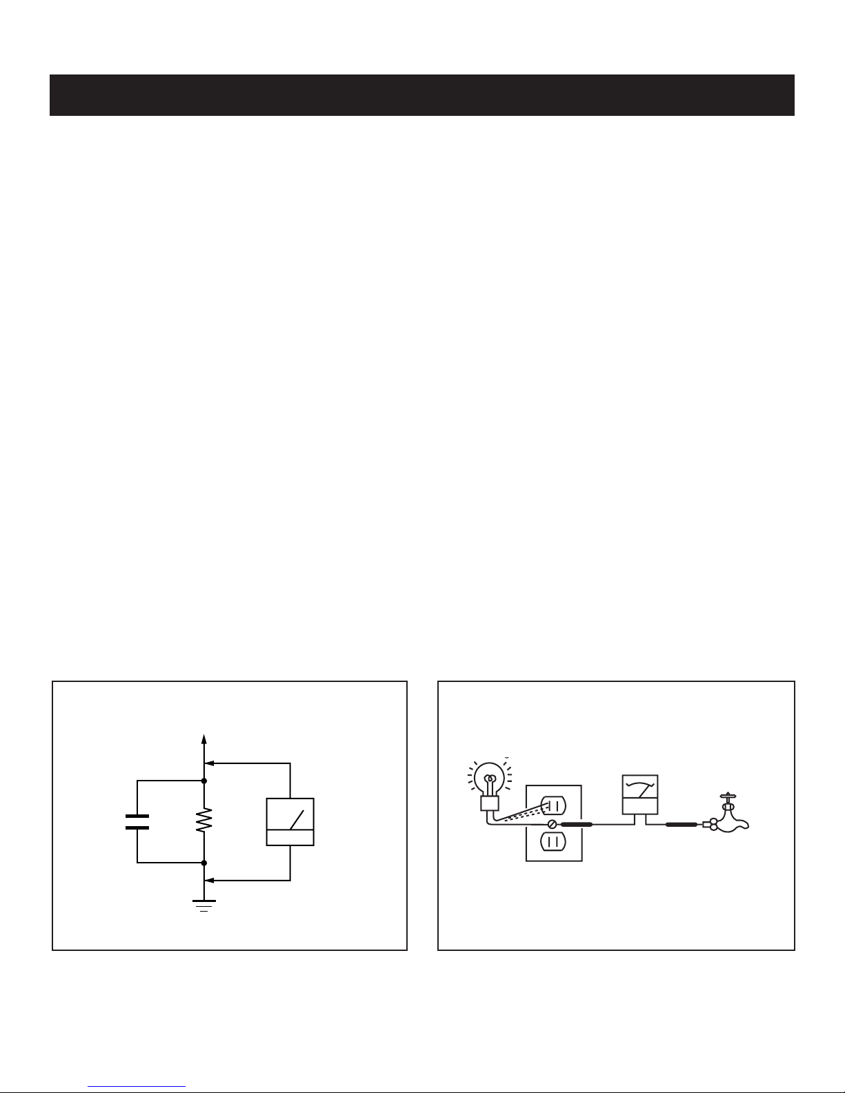
Leakage Test
The AC leakage from any exposed metal part to earth ground and from
all exposed metal parts to any exposed metal part having a return to
chassis, must not exceed 0.5 mA (500 microamperes). Leakage current
can be measured by any one of three methods.
1. A commercial leakage tester, such as the Simpson 229 or RCA
WT-540A. Follow the manufacturers’ instructions to use these
instructions.
2. A battery-operated AC milliampmeter. The Data Precision 245 digital
multimeter is suitable for this job.
3. Measuring the voltage drop across a resistor by means of a VOM
or battery-operated AC voltmeter. The “limit” indication is 0.75 V,
so analog meters must have an accurate low voltage scale. The
Simpson’s 250 and Sanwa SH-63TRD are examples of passive
VOMs that are suitable. Nearly all battery-operated digital multimeters
that have a 2 VAC range are suitable (see Figure A).
How to Find a Good Earth Ground
A cold-water pipe is a guaranteed earth ground; the cover-plate retaining
screw on most AC outlet boxes is also at earth ground. If the retaining
screw is to be used as your earth ground, verify that it is at ground by
measuring the resistance between it and a cold-water pipe with an
ohmmeter. The reading should be zero ohms.
If a cold-water pipe is not accessible, connect a 60- to 100-watt troublelight (not a neon lamp) between the hot side of the receptacle and the
retaining screw. Try both slots, if necessary, to locate the hot side on the
line; the lamp should light at normal brilliance if the screw is at ground
potential (see Figure B).
To Exposed Metal
Parts on Set
0.15 µF
Figure A. Using an AC voltmeter to check AC leakage. Figure B. Checking for earth ground.
1.5 kΩ
Earth Ground
KV-34DRC430/36DRC430
AC Voltmeter
(0.75 V)
AC Outlet Box
Ohmmeter
Cold-water Pipe
7
KV-34DRC430/36DRC430
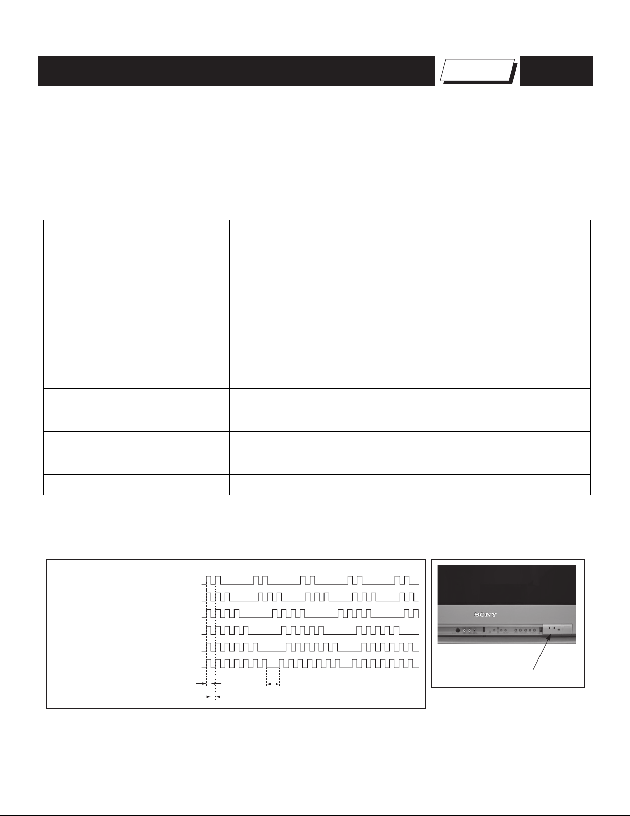
SELF-DIAGNOSTIC FUNCTION
Self Diagnosis
Supported model
The units in this manual contain a self-diagnostic function. If an error occurs, the STANDBY/TIMER LED will automatically begin to fl ash. The number
of times the LED fl ashes translates to a probable source of the problem. A defi nition of the STANDBY/TIMER LED fl ash indicators is listed in the
instruction manual for the user’s knowledge and reference. If an error symptom cannot be reproduced, the Remote Commander can be used to review
the failure occurrence data stored in memory to reveal past problems and how often these problems occur.
Diagnostic Test Indicators
When an error occurs, the STANDBY/TIMER LED will fl ash a set number of times to indicate the possible cause of the problem. If there is more than
one error, the LED will identify the fi rst of the problem areas.
Results for all of the following diagnostic items are displayed on screen. If the screen displays a “0”, an error has occurred.
No. of times
Diagnostic Item
Power does not turn on Does not light _______
+B Overcurrent (OCP)* 2 times 2:0 or 2:1
Low +B Overvoltage (OVP) 3 times 3:0 or 3:1
Vertical Deflection Stopped 4 times 4:0 or 4:1
White Balance Failure
(not balanced)
LOW +B OCP/OVP
(overcurrent/overvoltage)***
Horizontal Deflection
Stopped
STANDBY /
TIMER lamp
flashes
5 times 5:0 or 5:1
6 times 6:0 or 6:1
7 times 7:0 or 7:1
Display
Result
Probable Cause Location Detected Symptoms
• Power cord is not plugged in.
• Fuse is burned out (F501). (AY Board)
• H.OUT (Q5030) is shorted. (DZ Board)
• +B PWM (Q5003) is shorted.
(DZ Board)
• IC6505 is faulty. (DZ Board) • Has entered standby mode.
• 15V is not supplied. (DZ Board)
• IC5004 is faulty. (DZ Board)
• Video OUT (IC9001-IC9003) is faulty.
(CH, Board)
• CRT drive (IC2801) is faulty. (BY Brd.)
• G2 is improperly adjusted.**
• +5 line is overloaded. (AY, BY, MY
Boards)
• +5 line is shorted. (AY, BY, MY Brds.)
• IC504 is faulty. (AY Board)
• Power does not come on.
• No power is supplied to the TV.
• AC Power supply is faulty.
• Power does not come on.
• Load on power line shorted.
• Has entered standby mode after
Horizontal raster.
• Vertical deflection pulse is stopped.
• Power line is shorted or power
supply is stopped.
• No raster is generated.
• CRT cathode current detection
reference pulse output is small.
• No picture
• No picture
* If a +B overcurrent is detected, stoppage of the vertical deflection is detected simultaneously. The symptom that is diagnosed first by the
microcontroller is displayed on the screen.
** Refer to Screen (G2) in Section 2-5 of this manual.
*** If STANDBY/STEREO LED flashes six (6) times, unplug the unit and wait 10 seconds before performing the adjustment.
Display of Standby/Timer LED Flash Count
Diagnostic items Flash count
+B Overcurrent 2 times
Low +B Overvoltage 3 times
Vert. Deflection Stopped 4 times
White Balance Failure 5 times
Low +B OCP/OVP 6 times
Horiz. Deflection Stopped 7 times
Lamp ON 0.3 sec.
Lamp OFF 0.3 sec.
Stopping the Standby/Timer LED Flash
Turn off the power switch on the TV main unit or unplug the power cord from the outlet to stop the STANDBY/TIMER LAMP from fl ashing.
KV-34DRC430/36DRC430
Lamp OFF 3 sec.
Standby/Timer LED
* One fl ash count is not used for
self-diagnostic.
8
KV-34DRC430/36DRC430
Self-Diagnostic Screen Display
For errors with symptoms such as “power sometimes shuts off” or “screen sometimes goes out” that cannot be confi rmed, it is possible to bring up past
occurrences of failure on the screen for confi rmation.
To Bring Up Screen Test
In standby mode, press buttons on the Remote Commander sequentially, in rapid succession, as shown below:
DISPLAY
Channel 5 Sound volume - Power ON.
SELF DIAGNOSIS
2: +B OCP 0
3: +B OVP 0
4: VSTOP 0
5: AKB 1
6: LOWB 0
7: H-STOP 0
Numeral “0”
means that no fault was detected.
Numeral “1”
means a fault was detected one
time only.
101: WDT 24
Handling of Self-Diagnostic Screen Display
Since the diagnostic results displayed on the screen are not automatically cleared, always check the self-diagnostic screen during repairs. When you
have completed the repairs, clear the result display to “0”.
Unless the result display is cleared to “0”, the self-diagnostic function will not be able to detect subsequent faults after completion of the repairs.
Clearing the Result Display
To clear the result display to “0”, press buttons on the Remote Commander sequentially when the diagnostic screen is displayed, as shown below:
NOTE: This will also reset all user functions (including auto programming and picture settings)
8
ENTERChannel
Quitting the Self-Diagnostic Screen
To quit the entire self-diagnostic screen, turn off the power switch on the Remote Commander or the main unit.
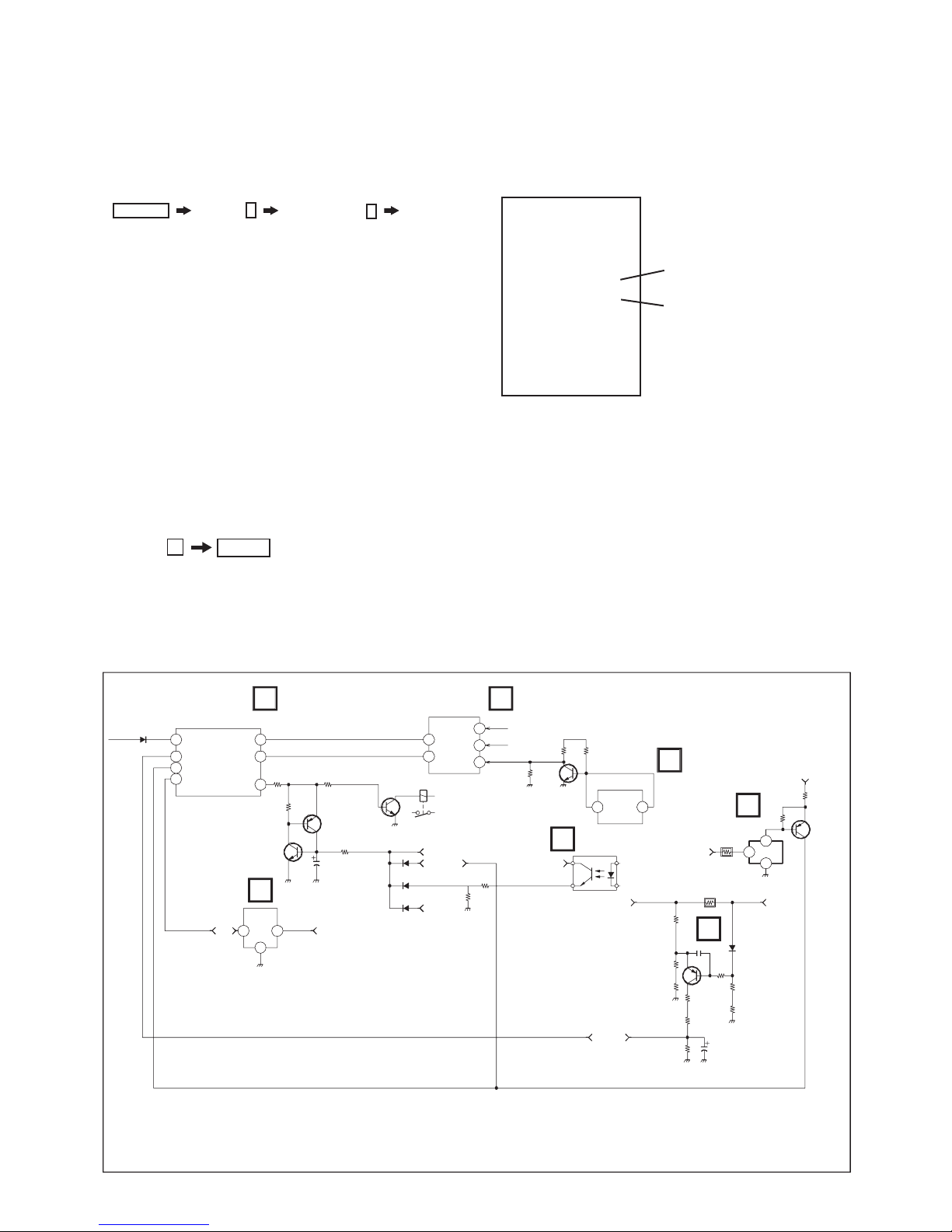
Self-Diagnostic Circuit
STBY-LED
IC2300
MAIN MICRO
STR
48
STBY-LED
44
OCP
45
OVP
43
LOW B ERR
AC RLY
5V UNREG 7V
MY
CLKO
29
DATO
30
69
Q6527
Q6530
ENABLE ON
LATCH
Q6532
LATCH
AY
IC504
SV REF
IO
O
IC2801
Y/C JUNGLE
SCL
26
25
SDA
RY6501
P_SW(-)
21
34
1K-PROT2
+B OVP
D6537
D6505
HV PROT
D5007
BY
AKB
58
CRT
35
VPROT
HPROT
VDY-
34
R5104 R5105
R5125
UNREG 11V
DZ
Q5018
INVERT
2
14
IC5007
H. PROT
MONITOR
DZ
PH6501
IN RUSH
OVER CURRENT
1
4
2
3
+B +B
Q5004
+ B COP
DETECT
+B OCP
DZ
IC6505
+B OVP
+B
R5013
1
DZ
D5005
5V
Q6522
2
3
FOLLOWER
KV-34DRC430/36DRC430
9

KV-34DRC430/36DRC430
+B overcurrent (OCP)
Occurs when excessive current fl ows through R5013. The increase in voltage across R5013 causes the output of Q5004 to go high, and this high
signal goes to the micro.
+B overvoltage (OVP)
IC6505 detects +B OVP condition and turns on Q6522. This sends a high signal to the micro and also shuts down the AC relay.
V-STO P
Occurs when an absence of the vertical defl ection pulse is detected by pin 24 of IC2801 (BY Board). Power supply will shut down when waveform
interval exceeds 2 seconds.
White Balance Failure
If the RGB levels* do not balance within 2 seconds after the power is turned on, this error will be detected by IC2801. TV will stay on, but there will be
no picture.
*(Refers to the RGB levels of the AKB detection Ref pulse that detects 1K).
Low B OCP/OVP
Occurs when set 5V is out.
Horizontal Defl ection Stopped
Occurs when either:
1) a +B overcurrent is detected (IC5007), or
2) overheating is detected (Thermistor TH5002).
KV-34DRC430/36DRC430
10
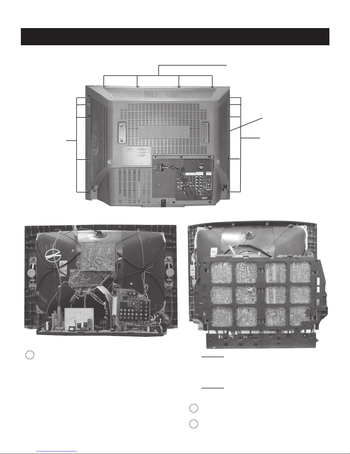
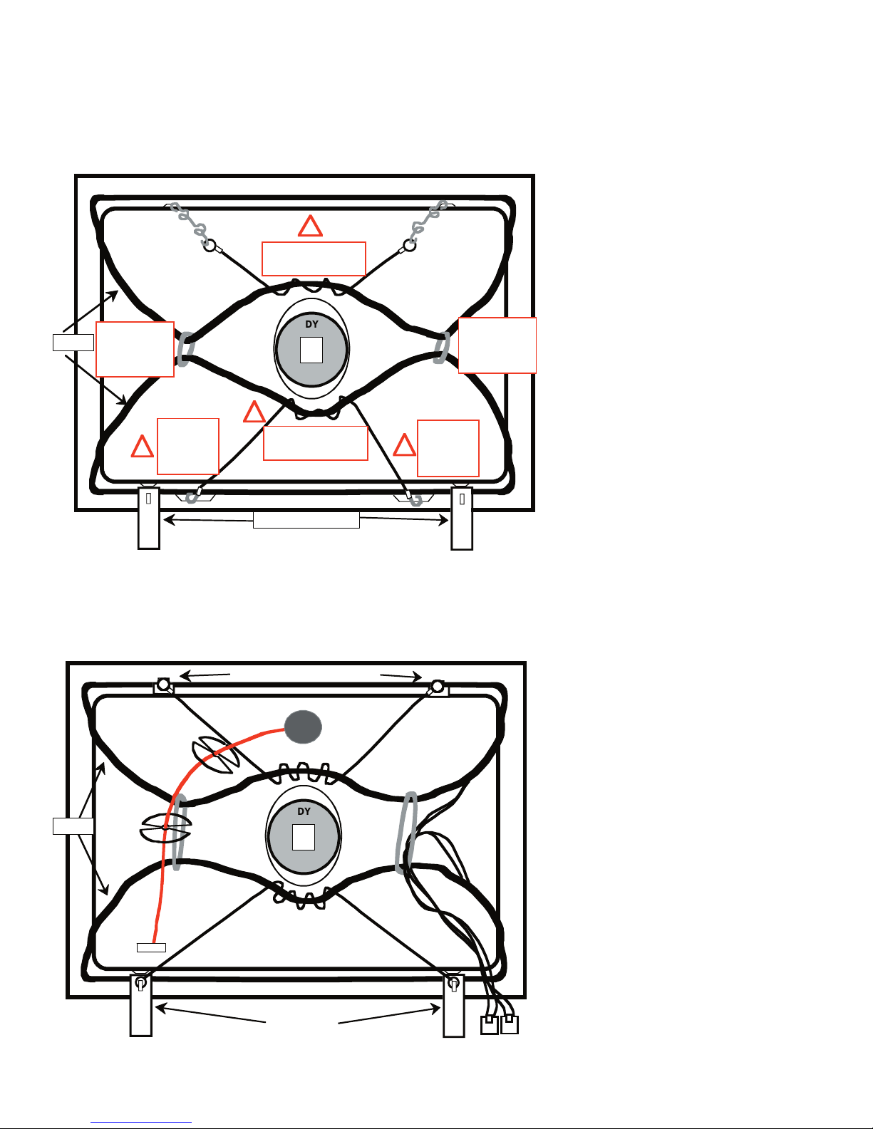
SECTION 1: DISASSEMBLY
KV-34DRC430/36DRC430
1-1. REAR COVER REMOVAL
5 Screws
+BVTP 4 x 16
TYPE2 TT (B)
1-2. CHASSIS ASSEMBLY REMOVAL
4 Screws
+BVTP 4 x 16
TYPE2 TT (B)
Rear Cover
5 Screws
+BVTP 4 x 16
TYPE2 TT (B)
1-3. SERVICE POSITION
1
Lift lever up on the right and left sides of the chassis
bracket and gently pull the chassis assembly away from
the bezel.
KV-34DRC430/36DRC430
CAUTION! - Heat sink on IC5004 is -15V. Do not to allow
heat sink to touch GND or any other components.
Heat sink on Q8018 VpK=250V. Do not touch or short to
GND or other components.
CAUTION! - Pay attention to Neck Assembly WY Board
wire harness to BY Board. The WY Board can easily break if
there is sudden or excessive tension on the harness.
Lift lever up on the right and left sides of the chassis bracket
1
and gently pull the chassis assembly away from the bezel.
Pull up and rotate both the AY and DZ Boards in order to
2
service the unit.
11

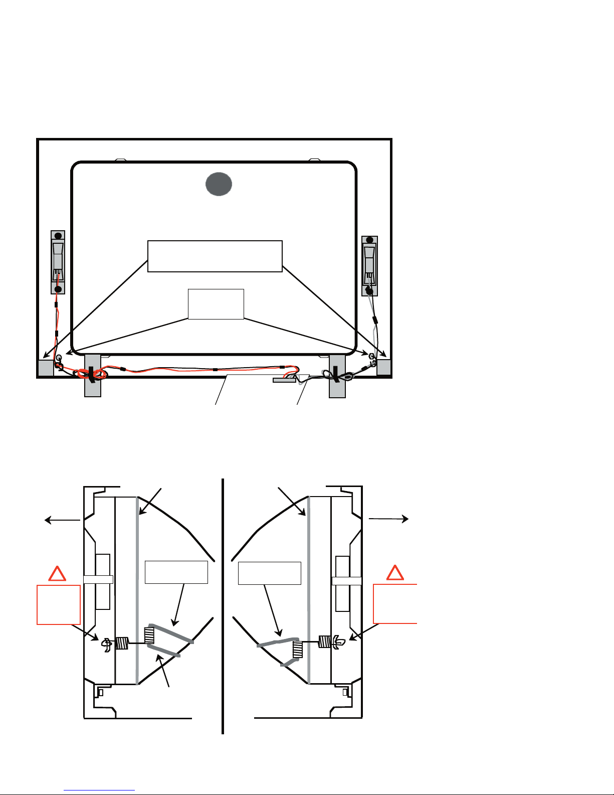
1-4. PICTURE TUBE REMOVAL
WARNING: BEFORE REMOVING THE ANODE CAP
High voltage remains in the CRT even after the power is disconnected. To avoid electric shock,
discharge CRT before attempting to remove the anode cap. Short between anode and CRT
coated earth ground strap.
1
6
5
2
9
4
7
10
1. Discharge the anode of the CRT and remove the
anode cap.
8
2. Unplug all interconnecting leads from the defl ection
yoke, neck assembly, degaussing coils and CRT
3
4
grounding strap.
3. Remove the CH Board from the CRT.
3
4. Remove the chassis assembly.
5. Loosen the neck assembly fi xing screw and remove.
6. Loosen the defl ection yoke fi xing screw and remove.
7. Place the set with the CRT face down on a cushion
and remove the degaussing coil holders.
8. Remove the degaussing coils.
9. Remove the CRT grounding strap and spring
tension devices.
10. Unscrew the four CRT fi xing screws [located on
each CRT corner] and remove the CRT
[Take care not to handle the CRT by the neck].
KV-34DRC430/36DRC430
Coated
Earth
Ground
Strap
ANODE CAP REMOVAL PROCEDURE
WARNING: High voltage remains in the CRT even after the power is disconnected. To avoid electric shock, discharge CRT before attempting to
remove the anode cap. After removing the anode cap, short circuit to either the metal chassis, CRT shield, or carbon painted on the CRT.
NOTE: After removing the anode cap, short circuit the anode of the picture tube and the anode cap to either the metal chassis, CRT shield or carbon
painted on the CRT.
REMOVAL PROCEDURES
a
Turn up one side of the rubber cap in
the direction indicated by arrow a .
b
Use your thumb to pull the rubber
cap fi rmly in the direction indicated
by arrow b .
HOW TO HANDLE AN ANODE CAP
1. Do not use sharp objects which may cause damage to the surface of the anode
cap.
2. To avoid damaging the anode cap, do not squeeze the rubber covering too
hard. A material fi tting called a shatter-hook terminal is built into the rubber.
3. Do not force turn the foot of the rubber cover. This may cause the shatter-hook
terminal to protrude and damage the rubber.
Anode Button
When one side of the rubber cap separates from
the anode button, the anode cap can be removed
by turning the rubber cap and pulling it in the
direction of arrow c .
c
KV-34DRC430/36DRC430
12
KV-34DRC430/36DRC430
]
y
w
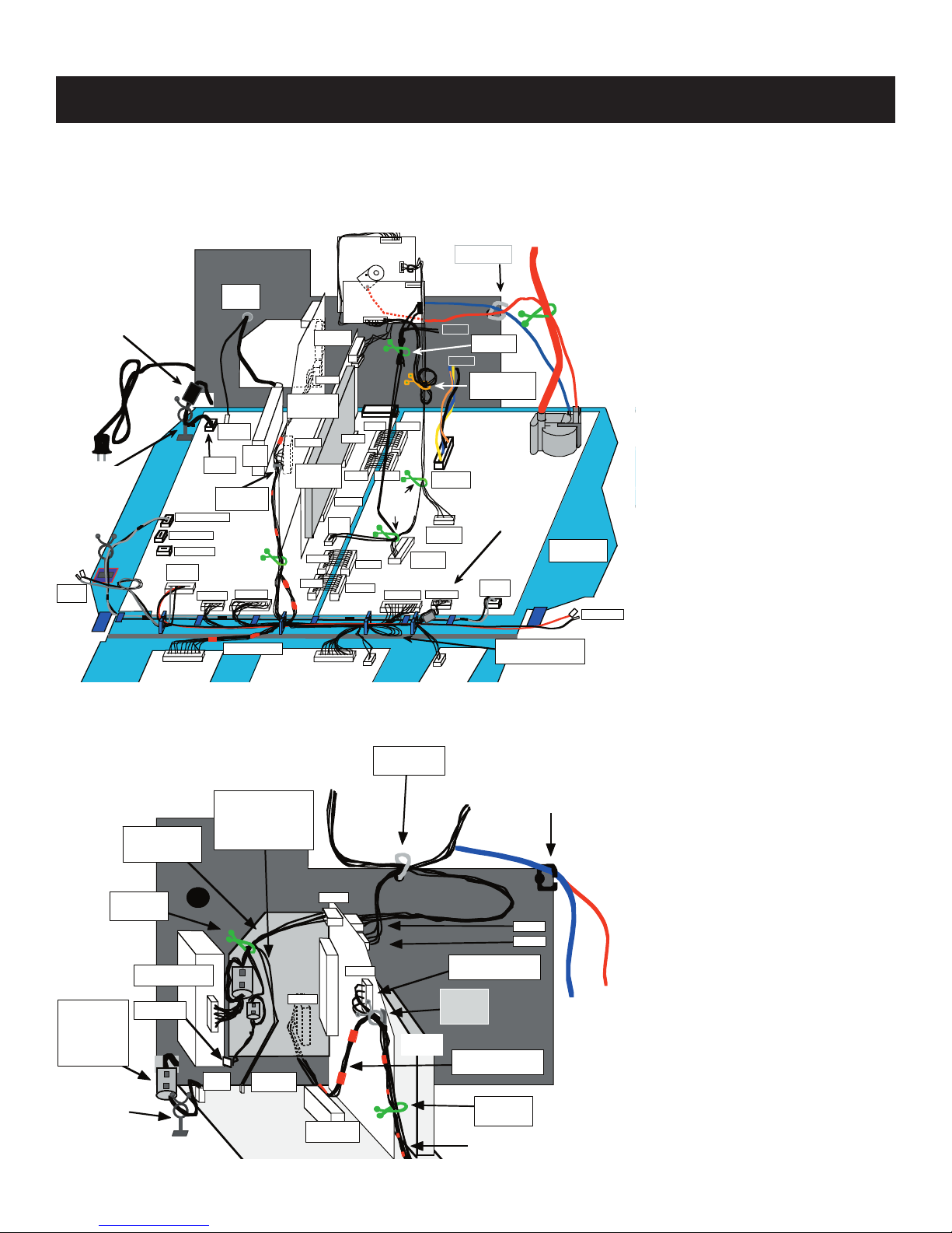
CABLE WIRE DRESSING
NOTE: IF THE WIRE DRESSING IS NOT DONE PROPERLY, IT MAY CAUSE DISTORTION
CHASSIS ASSEMBLY
CLIP-ON
FERRITE
1-500-386-11
or
1-500-586-11
AC Power Cord
w/filter plug
1-769-837-13
12mm Purse Lock
(38mm height)
4-072-499-01
12mm Purse Lock
(38mm height)
4-072-499-01
To
Speaker
HB[Y
[AY]
CN514 (AC LINE)
CN505 (DGC)
CN504 (DGC)
CN527 8P
SPEAKER
CN1100
CN503
MAIN AC
Angled Purselock
A-SIDE of [MY]
4-355-912-21
CN526 5P
F-Pin Plug
w/GND lead
1-829-088-11
CN501
(Terminal)
9mm
Purse
Lock
CN524 12P
H-BRACKET
[UY]
MAIN
Tu
[HAX]
[MY]
CN2301
[BY]
CN521
CN900
CN2805 11P
RGB on CH
CN1501
CN513
CN903
to CY
CN1000
[CY]
CN9102
5P
CN510
CN509
CN5011
CN6506
CN1002
BUS CONN
CN510
CN9001
CN9102
[WY]
CN5001
CN9002
CN9103
CN5009
5mm
Purse
Lock
CN5509 9P
to [VM]
CN6503 5PCN6504 12P
CN1052
TO DY
DY CONN
CN5002
CN5003
200V
Box-Purselock
4-065-850-11
5mm
Purse Lock
TO DY
11mm
Purse Lock
p/n: 3-703-983-02
[HCX]
G2 LEAD
[DZ]
5P Conn. Assy.
w/Ferrite Core
1-900-807-16
CN6502
(AC LINE)
CN2301 --> CN1000 10P
1-900-808-01
LOOP extra wires in clip here.
HV LEAD
5mm
Purse
Lock
MAIN
BRACKET
FOCUS LEAD
To Speaker
U-BRACKET WIRE DRESSING
1-900-805-24
Terminal Wire Assy.
And Ferrite Core
(with one loop)
1-500-082-11
CN 503
AC
[AY]
[UY]
CN518
TERMINAL
CN1501
CLAMP-ON
Ferrite Bead
1-500-386-11
or 1-500-586-11
w/ NO Loop
on AC Cord
1-769-837-13
Purselock
4-072-499-01
Attached to Main
Bracket Assembl
1-900-808-41
14P Conn. Assy.
w/Ferrite Core
9mm
Purse Lock
3-703-982-02
P-Shield
TERMINAL TAB
ON P-SHIELD
To CH Bd
CN9001 11P
1-900-806-85
CN2304
Tuner
CN2301
[MY]
CLAMP
4-857-472-01
+ 3X12mm Scre
[BY]
To WY Bd
CN9102 6P
1-900-808-32
1-900-808-01
10P Conn. Assy.
CLP2002
Purselock
(angled)
4-355-912-21
1-900-806-83
11P Conn. Assy.
9mm
Purse Lock
3-703-982-02
To HA/HBY Bd
CN2805
CN2803
Clip
G2/Focus
Lead Here
Wire Holder
4-065-850-11
TO FBT
“Focus”
TO FBT
1-900-805-19
“G2”
1-900-808-42
KV-34DRC430/36DRC430
13
G2 WIRE ROUTING CAUTION POINT
KV-34DRC430/36DRC430
Dress wire in
“L” Shape.
FBT
O.K. CONDITION
SIDE VIEW
Wire Holder
p/n: 4-065-850-11
G2 Wire MUST be routed correctly
so that the wire does NOT touch
Rear Cover (Causes “Buzzing” sound)
Route wire in front of U-Bracket!
FBT
U-Bracket
BY BOARD WIRE DRESSING
REAR VIEW
!
U-Bracket
Wire Holder
p/n: 4-065-850-11
N.G CONDITION
SIDE VIEW
N.G!
Wire can touch
Rear Cover!!
FBT
U-Bracket
CN9106
[CH]
1-900-806-85
11P Conn. Assy.
CLAMP
4-857-472-01
+ 3X12mm Screw
U-BRACKET
[WY]
CN2301
[MY]
Tuner
KV-34DRC430/36DRC430
[BY]
CN9102
CN9101
1-900-808-32
6P Conn. Assy.
CN2805
ON BY-Bd
CN2803
ON BY-Bd
14
KV-34DRC430/36DRC430
G2 & FOCUS LEAD WIRE DRESSING
CAUTION POINT
[CH]
CLP9003
CRT SOCKET
CN9109
CLP9002
CN9003
ECG
CN9004
ECG
FOCUS
LEAD
G2
Dress
wires in
Clamp on
U-Bracket
SIDE VIEW
[CH]
B-Side
!
Push Wire Down
HERE.
Dress wires so
they do NOT
touch B-Side of
WX-Board!
BEFORE Installing CH-Board to CRT Neck
PUSH down G2 Lead AND Focus Lead. The wires
must NOT touch B-side of WY-Board!
[WY]
FOCUS Lead
G2 Lead
Push Wire Down
HERE
CLP9002
TO [BY]
CN 2805
11P
[CH] /[WY] /[HV]
CLP9001
[CH]
CN9003
CN9004
ECG
ECG
[WY]
CN9100
TO [DL]
CN 5808
4P
TO [D]
CN 5509
12P
CN9001
RGB
CN9109
G2
CN9102
TO [BY]
CN 2803
6P
CN9002
200V
CN9101
(Rot. Coil)
Clip BOTH
Anode &
Focus Leads
HV-Lead Spacer
See CRT dress
diagram for
details. Number
of
spacers vary by
model.
CLP9003
TO [D]
CN5003
3 wire - 4P
HV-Lead Spacer
G2
TO FBT
Focus Lead
5mm
Purse
Lock
DY LEAD DRESSING
DGC Purselock
P/N: 4-081-411-02
ATTACH DY LEADS to DGC
Purselock
4-081-411-02
KV-34DRC430/36DRC430
DY
Rotation
COIL
NOTE: Do not apply a LOOP on the
leadstotakeupslack.
The leads can be slack ABOVE the
purselock.
15
F-PIN CABLE WIRE DRESSING
KV-34DRC430/36DRC430
P-Shield
CN 503
AC Conn.
CN501
TERMINAL
[AY]
1-829-088-11
P-F Cable
w/Gnd. Lead Terminal
(NOT dressed with
other connectors)
[UY]
Tuner
[MY]
CAUTION:
MAKE SURE Ground Lead
Terminal is attached to
CN501 (not CN528)!!
[BY]
DGC LEAD WIRE DRESSING
STEP1:
Make a loop in leads
and route loop BEHIND
The DGC Coil.
STEP 2:
Thread both connector
housings through the
loop in lead wires.
STEP 3:
Plug in connector
housings into the
[AY] Board using the
loop to take up slack.
DY
Cable Tie
4-041-041-02
KV-34DRC430/36DRC430
16
ECG WIRE DRESSING (KV-36DRC430 ONLY)
NOTE2: There are
2 Leads (TOTAL 4
Wires) to connect
2-022-978-01
Wire Clip (2 Places)
NOTE: Leads are
dressed inside
Rotation Coil.
Rotation
COIL
ECG-P/N
1-900-808-30 - 30 WCRT
1-900-808-31 - 34W CRT
to CH-Board
DY
SPRING (2 places)
Integral part of
the Ground wire
KV-34DRC430/36DRC430
CRT BRKT
ECG WIRE DRESSING (KV-34DRC430 ONLY)
(Earth Coating Ground)
Caution Points:
1. Make sure braided ECG wire loop does not
twist, and stays flat on CRT surface.
2. Do not pull excessively on the tension spring.
DY
NOTE: Leads are
dressed inside
Rotation Coil.
3. If the spring appears warped or stretched,
replace entire parts. The braided ECG wire
CANNOT sag on the CRT, and must remain
under tension.
Earth Coating
Ground Wire (ECG)
32”: 1-900-808-29
36”: 1-900-808-28
Rotation
COIL
NOTE2: There are
2 Leads (TOTAL 4
Wires) to connect
to CH-Board
Integral Spring
2-Places
CRT BRKT
KV-34DRC430/36DRC430
17
DGC ASSEMBLY CAUTION POINT (KV-36DRC430 ONLY)
KV-34DRC430/36DRC430
DGC
2-022-978-01
Wire Clip (2 Places)
Caution:
Make sure Cable
Tie is TIGHTENED
once CRT is in
Vertical postion.
!
1-910-000-13
DGC Restraint Cable
Caution:
Make sure
hook is
secure on CRT
pierce!
Wrap x4 LOOP (for 30W)
Wrap x2 LOOP (for 34W)
!
Wrap x4 LOOP (for 30W)
Wrap x2 LOOP (for 34W)
!
NO SLACK ON WIRE!
DY
NO SLACK ON WIRE!
1-900-803-55
DGC Restraint Cable
CRT BRACKET
CRT WIRE DRESSING (KV-34DRC430 ONLY)
Caution:
Make sure
hook is
!
secure on CRT
pierce!
Caution:
Make sure Cable
Tie is TIGHTENED
once CRT is in
Vertical postion.
DGC
Cable Holder
4-084-918-01
x2
To FBT
Cable Tie
4-041-041-02
DGC Clip (p/n: 4-102-284-01)
Rotation
COIL
DY
Cable Tie
4-041-041-02
1-900-804-64
DGC Restraint Cable
(w/ x4 loops around DGC)
CRT BRKT
1-900-804-64
DGC Restraint Cable
(w/ x4 loops around DGC)
KV-34DRC430/36DRC430
18
SPEAKER ASSEMBLY WIRE DRESSING
NOTE: Keep speaker wires away from pocket
in the beznet (gray area).
The wires can get pinched when installing
the rear cover (due to boss on the rear cover).
CLAMP
4-857-472-01
w/ 4x16mm screw
7-685-663-71
KV-34DRC430/36DRC430
CRT Bracket
ECG ASSEMBLY CAUTION POINT
CRT Frit-Line
FRONT
Make sure braided
!
Caution:
Clip spring on
the OUTSIDE
of the CRT
pierce.
SPEAKER
wire does not twist or
sag on CRT surface.
CN527 8P
[AY]
CRT Frit-Line
Make sure braided
wire does not twist or
sag on CRT surface.
CRT Bracket
SPEAKER
FRONT
!
Caution:
Clip spring on
the OUTSIDE
of the CRT
pierce.
Earth Coating Groung
[ECG]
KV-34DRC430/36DRC430
19
SECTION 2: SET-UP ADJUSTMENTS
KV-34DRC430/36DRC430
The following adjustments should be made when a complete
realignment is required or a new picture tube is installed.
These adjustments should be performed with rated power supply
voltage unless otherwise noted.
The controls and switch should be set as follows unless otherwise
noted:
VIDEO MODE: STANDARD (RESET)
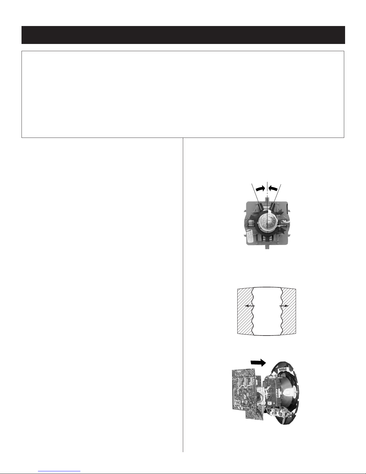
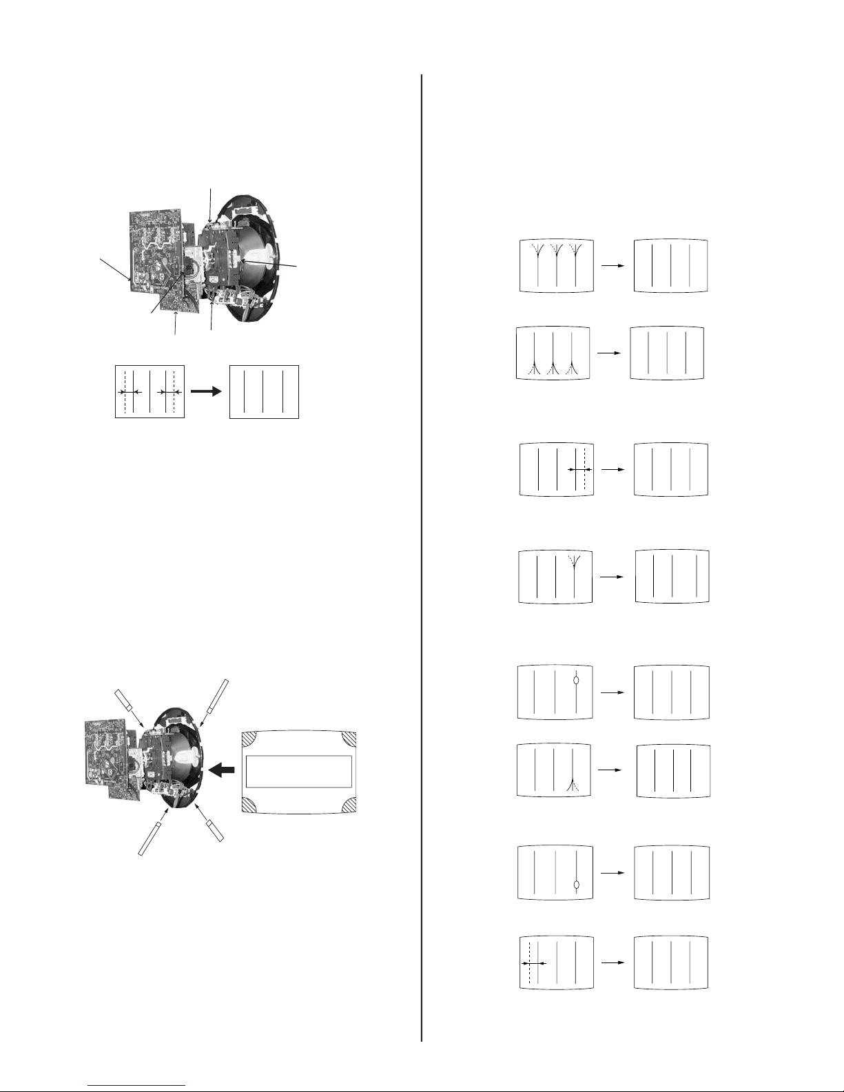
2-1. BEAM LANDING
Preparation:
• Use cross hatch signal to rough adjust focus, G2 and then input a
white pattern signal.
• Face the picture tube in an East or West direction to reduce the
infl uence of geomagnetism.
• Remove all magnets, wedges, and permalogy strips.
• Confi rm data in service mode to match with CRT screen size.
•
Set 2170D-1 to their default settings.
• VCEN 31
• VPIN 15
• HTPZ 15
•
Set 2170D-2 to their default settings.
• PPHA 20
• VANG 31
• LANG 31
• VBOW 31
• LBOW 31
•
Set 2170D-4 to their default settings.
• CXA8070 to their default settings.
•
Set all user compensations to their default settings.
•
Set landings to their default settings.
• LT Left Top LCC Control 127
• LB Left Bottom LCC Control 127
• RT Right Top LCC Control 127
• RB Right Bottom LCC Control 127
NOTE: Do not use the hand degausser; it magnetizes the CRT
Perform the adjustments in order as follows:
1. Beam Landing
2. Convergence
3. Focus
4. Screen (G2)
5. White Balance
Test Equipment Required:
1. Color Bar Pattern Generator
2. Degausser
3. DC Power Supply
4. Digital Multimeter
1. Input white pattern from pattern generator. Set the PICTURE control
to maximum, and the BRIGHTNESS control to standard.
2. Loosen the defl ection yoke mounting screw, and set the purity
control to the center as shown below:
Purity Control
Figure 1
3. Input a green pattern from the pattern generator.
4. Move the defl ection yoke backwards, (See Figure 1) and adjust with
the purity control so that green is in the center and red and blue are
even on both sides.
Blue Red
Green
5. Move the defl ection yoke forward, and adjust so that the entire screen
becomes green.
KV-34DRC430/36DRC430
20
KV-34DRC430/36DRC430
6. Switch over the raster signal to red and blue and confi rm the
condition.
7. When the position of the defl ection yoke is determined, tighten it with
the defl ection yoke mounting screw.
8. Move the yoke up and down and/or side to side to fi nd the best
geometry. Once the best position is confi rmed mount the rubber
wedges to hold the yoke position in place for best geometry.
9. If landing at the corner is not right, adjust it by using the disk
magnets.
Disk magnets
or rotatable disk
magnets correct
these areas (a-d)
b
d
Purity control
corrects this area
ba
cd
Deflection yoke positioning
corrects these areas
a
c
4. Tilt the V.STAT magnet and adjust static convergence to open or
close the V.STAT magnet
1
B
G
R
B
G
R
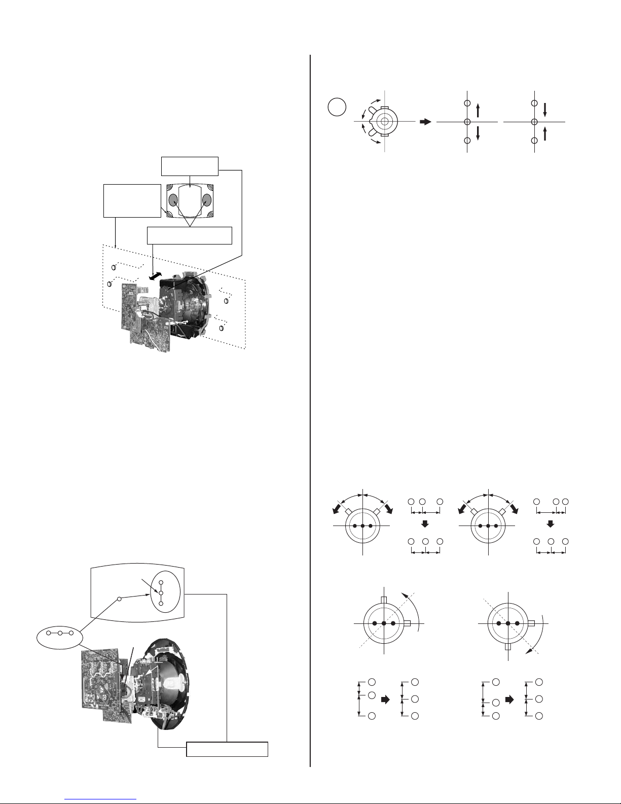
2-3. V-PIN AND V-CEN ADJUSTMENT
Preparation:
• Input a cross hatch pattern signal.
• Set Video Mode to: Standard (Reset)
• For all 4x3 CRT, VPIN data has separate register for full and
V-compress. Adjust both modes if needed.
• For all 16x9 CRT’s, adjust VPIN in normal mode for straightness of
horizontal line.
1. Adjust service mode CXA2170D-1 05 V-CEN so that the top pin and
bottom pin are symmetrical from top to bottom.
2. Adjust service mode CXA2170D-1 06 V-PIN so that the top pin and
bottom pin are symmetrical from top to bottom.
3. Horizontal lines should be straight from left to right. Check landing for
side effect.
2-2. CONVERGENCE
2-3.1. OPERATION OF BMC (HEXAPOLE)
Preparation:
• Set the CONTRAST and BRIGHTNESS control to standard (reset).
• Input a cross hatch pattern signal.
2-2.1. VERTICAL AND HORIZONTAL STATIC
The respective dot positions result from moving each magnet interact.
Perform the following adjustments while tracking.
1. Use the BMC tabs to adjust the red, green and blue dots so that
CONVERGENCE
1. Set dynamic convergence to default values (as in 2-1 Beam Landing)
or disconnect the dynamic convergence before adjusting static
convergence (CN903), except for minor touch-up.
2. Adjust H.STAT convergence, RV9001, on CH Board to converge
red, green, and blue dots in the center of the screen.
3. Adjust V. STAT magnet to converge red, green and blue dots in the
center of the screen.
R G B
Center dot
RV9001
H-STAT
R
G
B
MAGNET
they line up at the center of the screen (move the dots in a horizontal
direction).
HMC Correction HMC Correction
A<B
R
RGB
A=B
VMC Correction
GB
AB
AB
VMC Correction
A>B
A=B
GB
R
AB
RGB
AB
V.STAT magnet
KV-34DRC430/36DRC430
C<D
C
G
D
C=D
R
B
R
G
B
C<D
C
G
D
C=D
R
B
R
G
B
21
KV-34DRC430/36DRC430
2-3.2. TLH PLATE ADJUSTMENT
Preparation:
• Input a cross hatch pattern signal.
• Adjust unbalanced horizontal convergence of red and blue dots by
adjusting the TLH Plate on the defl ection yoke.
TLV
CH Board
RV9001
B R
(R)(B)
WY Board
(B)(R)
R B
XCV
TLH+
TLH-
1. Adjust XCV core to balance X axis.
2. Adjust the vertical red and blue convergence with V.TILT (TLV VR).
Note: Perform adjustments while tracking Item 1.
Note: Restore dynamic convergence when static convergence
adjustments are complete.
TLH Plate
2-3.4. DYNAMIC CONVERGENCE
ADJUSTMENTS
• Set dynamic convergence using the following service registers. Note
areas of change.
• Only H-component can be corrected, for vertical component use
permalloy to compensate.
0. YBWU (Upper Y-BOW)
BR BR
1. YBWL (Lower Y BOW)
BR BR
2. RSAP (Right H AMP)
RB
3. RUBW (Right Upper BOW)
BR
2-3.3. SCREEN-CORNER CONVERGENCE
Preparation:
• Input a cross hatch pattern signal.
1. Affi x a permalloy assembly corresponding to the misconverged areas.
b
a
ab
a-d: screen-corner
misconvergence
c
d
c
d
4. RUMB (Right Upper Middle BOW)
5. RLBW (Right Lower BOW)
6. RLMB (Right Lower Middle BOW)
7. LSAP (Left H AMP)
BR
RB
BR
KV-34DRC430/36DRC430
BR
22
8. LUBW (Left Upper BOW)
y
BR
KV-34DRC430/36DRC430
9. LUMB (Left Upper Middle BOW)
BR
10. LLBW (Left Lower BOW)
BR
11. LLMB (Left Lower Middle BOW)
BR
12. CADJ Fix 29
2-4. FOCUS ADJUSTMENT
Confi rm neck assembly Z axis position. (See Figure 1)
1. Input a dot signal.
2. Set Video Mode to STANDARD.
3. Adjust focus VR counter clockwise (Over-Focus) to confi rm the dot’s
shape. Center should be very slightly oval with left and right sides
balanced.
4. Input a HD monoscope signal.
5. Confi rm center focus with focus VR.
KV-34/36 DRC430
CRT: 34RSN/36RV2 (NON-super-fi ne pitch and round fannel)
Neck Assy:NA328 (VA-type, square pin assignment, VPIN harness)
Over Focus
Focus
Screen (G2)
HVD
DQP Dot Pattern
Upper Corner
Center Horizontal Line
Center Dot Slightly Oval
Lower Corner
Note: Changing neck assembly position will affect corner convergence.
2-4.1. DYNAMIC FOCUS/DYNAMIC QUADRA-
POLE DATA
Normally, no adjustments are necessary for these systems. If for some
reason the data is lost, use the data from Table 1 on Page 24:
1. Write the data from any non-vertically compressed mode, then
use the CPY1 function (CXA2170D-4 Item 6) to copy the data to the
vertical compressed modes.
Note: V-compressed data is identical to non-v-compressed
data. Service personnel with a trained eye can adjust the DF or
DQP registers to adjust DF phase (Item 7) or DQP phase (Item 8),
respectively, to balance left and right focus. Refrain from adjusting
more than 5 steps from table data below. Further adjustment indicates
a circuit problem -- troubleshoot to cause.
CAUTION: Be sure that Neck Assembly is in the proper location.
Mark position before moving or replacing neck assembly.
G3
G2 Neck-Ass
G1
Center T olerance: +/- 0.5mm
G1 Cu p Hol der
: NA3 28
Figure 1
KV-34DRC430/36DRC430
(See Section 2-4 Figure 1 - before changing DF/DQP data or
troubleshooting circuit when DF/DQP is suspect.)
Procedure to adjust or check:
1. Short Q8018 B-Gnd to disable DF. B Mark is on the circuit board.
Circuit connection changes should always be done with the power off.
CAUTION: Q8018 heatsink is live and peak voltage is 250V.
2. Input a cross hatch signal.
23
KV-34DRC430/36DRC430
3. Change CXA2170-P2 item 2 RGBS to 2 to make green only.
1. Overfocus to adjust DQP phase. Adjust the data
(CXA2170-D4 item 8) to balance left and right vertical line width.
2. Once DQP is balanced, remove the short from DF circuit and
refocus the set.
3. Adjust DF (CXA2170-D4 item 7) to balance left and right vertical
line width.
4. Reconfi rm focus performance.
34DRC 36DRC
QPAM 25 45
QPAV 40 47
QPAP 6 6
QPDC 17 42
QPDV 52 63
QPDP 6 6
DF 36 36
DQP 37 37
Table 1
2-5. SCREEN(G2)
1. Input composite white fi eld into Video 1.
2. Set to service mode and adjust as follows:
1. Set to Service Mode and adjust as follows:
2170P-2
NO. Name Control Function Avg. Data
01 RGBS R ON 4
2. Connect oscilloscope to Pin 1 of CN9001 (R.DRV) on the CH Board.
3. Adjust contrast according to the service mode item: SPIO.
2103-1
NO. Name Control Function
02 SCON SUB-CONT
white
VR1
black
VR2
GND
VR
(34DRC) = 1.92 ± 0.05 Vpp
(36DRC) = 1.92 ± 0.05 Vpp
4. Write data from Step 3 above, into memory.
(Fig. 1) Opeartion Procedure Standards Notes
1) In Full mode, apply changes in Fig. 1
CXA2170P-2 PICO 1-> 0
2) Mount G2 adjustment jig. Adjust Cathode
170 +/- 5 (V
DC
)
voltage if the standard is not met. Standard 34RSN, 36RV2
varies by CRT size.
175 +/- 5 (V
DC
)
3) Adjust G2 by Flyback transformer (T8001).
4) Return data changes in 1) to original condition.
2-6. PICTURE QUALITY ADJUSTMENTS
Preparation:
• Set PRO MODE (Reset).
1. Input signal (480i Composite):
• Color Bar Video 75 IRE (White) 75% modulation 7.5% Set-up.
• Color Bar RF 75 IRE (White) 75% modulation 7.5% Set-up.
2-6.1. VIDEO INPUT - SUB CONTRAST
ADJUSTMENT
Preparation:
• Input a Color Bar signal to VIDEO 1 (75 IRE 75%).
• Set picture mode: Single (Full) (PRO MODE Reset).
• Picture: Max
• Color: Min
KV-34DRC430/36DRC430
24
KV-34DRC430/36DRC430
2-6.2. VIDEO INPUT - SUB HUE/SUB COLOR
ADJUSTMENT
Preparation:
• Input a Color Bar signal to VIDEO 1 (75 IRE 75%).
• Set picture mode: Single (Full) (PRO MODE Reset).
• Picture: Max
1. Set to Service Mode and adjust as follows:
2170P-2
NO. Name Control Function Avg. Data
01 RGBS R ON 4
2. Connect an oscilloscope to Pin 5 of CN9001 (B. DRV) on the CH
Board.
3. Adjust color according to Service Mode for SCLO.
4. Adjust color according to Service Mode for SHUO.
2103-1
NO. Name Control Function
03 SCOL SUB-COL
04 SHUE SUB-HUE
7
VB4
2-6.3. RF INPUT - SUB CONTRAST
ADJUSTMENT
Preparation:
• Input a Color Bar signal to RF (75 IRE 75%).
• Set picture mode: Single (Full) (PRO MODE).
• Picture: Max
• Color: Min
1. Set to Service Mode and adjust as follows:
2170P-2
NO. Name Control Function Avg. Data
01 RGBS R ON 4
2. Connect an oscilloscope to Pin 1 of CN9001 (R. DRV) on the CH
Board.
3. Adjust contrast according to service mode for SCON.
2103-1
NO. Name Control Function
02 SCON SUB-CONT
COLOR: VB1 < VB4 (=20mV ± 200 mV)
HUE: VB2 < VB3 (=20mV ± 200 mV)
5. Write data into memory.
VB3VB2VB1
white
VR1
black
VR2
VR
(34DRC) = 1.92 ± 0.05 Vpp
(36DRC) = 1.92 ± 0.05 Vpp
4. Write data from Step 3 above, into memory.
GND
KV-34DRC430/36DRC430
25
KV-34DRC430/36DRC430
2-6.4. RF INPUT - SUB HUE/SUB COLOR
ADJUSTMENT
Preparation:
• Input a Color Bar signal to RF (75 IRE 75%).
• Set picture mode: single (FULL) (PRO MODE Reset).
• Picture: Max
1. Set to Service Mode and adjust as follows:
2170P-4
NO. Name Control Function Avg. Data
01 RGBS R ON 7
2. Connect an oscilloscope to pin 5 of CN9001 (B. DRV) on the CH
Board.
3. Adjust color according to Service Mode for SCOL.
4. Adjust color according to Service Mode for SHUE.
2103-1
NO. Name Control Function
03 SCOL SUB COLOR
04 SHUE SUB HUE
2-7. WHITE BALANCE (CRT) AND SUB
BRIGHT ADJUSTMENT
Preparation
• Input an all white 480I (15.734 KHz) signal into the VIDEO 1 input
terminal to perform the White Balance (highlight, cut-off) adjustments.
The parameters to adjust are in the CXA2170P1 in Service Mode.
• Set Picture Mode: Single (FULL) ( PRO MODE Reset)
• Picture: Max
• Color: Min
WHITE BALANCE ADJUSTMENT PROCEDURE (Compos ite White Field Signal into Video 1)
Old Calibration R/G
Highlight/Cutoff 29RSN/29RSEN .790 .903
9300K + 8MPCD
Specification WB701
Condition Registers BDRV 2170P-1-08
(R/G 1.000, B/G 1.000) 32RVE/32RV .775 .915
New Calibration Preset 34RSN .689 .883
Highlight/Cutoff
10,900K + 2MPCD 36RV2 .745 .905
(R/G 1.007, B/G 1.139)
Picture Mode: Single (Full) RDRV (fixed)** 2170P-1-06
Picture Setting:Pro
Color Temp: Neutral Adjustment
Picture: 63 write to 86h:01h:FFh (Service Mode)
Color: 0 write to 86h:03h:00h RCUT fixed)** 2170P-1-09
38RSN .679 .872
GDRV 2170P-1-0
GCUT 2170P-1-10
BCUT 2170P-1-11
** Data will differ by model
B/G
2-7.1. COLOR OFFSET ADJUSTMENT
PROCEDURE
COLOR: VB1 < VB4 (=20mV ± 200 mV)
HUE: VB2 < VB3 (=20mV ± 200 mV)
5. Write data into memory.
Preparation:
• Input an all white (30 IRE) signal to the specifi ed input.
• Adjust the white balance using the specifi ed registers.
VB4
• Set picture mode: Single (FULL) (PRO MODE Reset)
• Color: Max
VB3VB2VB1
VIDEO 1
CXA2170P1
NO. Name Control Function
3 CBOF CB OFFSET
4 CROF CR OFFSET
VIDEO 5
CXA2170P1
NO. Name Control Function
3 CBOF CB OFFSET
4 CROF CR OFFSET
VIDEO 7 -
HDMI 480i Signal
CXA2170P1
NO. Name Control Function
3 CBOF CB0F (FROM VIDEO 5) + 3
4 CROF CR0F (FROM VIDEO 5) - 4
KV-34DRC430/36DRC430
26
KV-34DRC430/36DRC430
2-8. H RASTER CENTER ADJUSTMENT
Preparation:
• Input a monoscope signal.
• Set to NTSC (DRC) mode.
1. Set to Service Mode and adjust as follows:
CXA2170P-2
NO. Name Control Function Data
05 AGNG AGING 1, AGING 2 2
CXA2170D-2
NO. Name Control Function Avg. Data
01 HPOS Horiz Position 34
02 HSIZ Horiz Size 34
CXA2170D-3
NO. Name Control Function Avg. Data
00 HBLK Blanking Enable 0
2. Reduce HSIZ to see sides of raster. (See Figure A)
3. Adjust H-Center with CXA2170D-2.
4. Adjust to the best screen position with H-CENT and write data.
5. Restore aging, HSIZ and HBLK to original condition.
2-9. PICTURE DISTORTION ADJUSTMENTS
2-9.1. NTSC (DRC) FULL MODE
ADJUSTMENT
1. Face the picture tube in an east-west direction. (For best condition.)
2. Input a monoscope and crosshatch signal.
3. Adjust the picture distortion with these two signals to balance the best
condition between the two.
Use the CXA2170-D1 and -D2 adjustable data items shown here.
4. Complete V-PIN and V-CEN adjustments fi rst and adjust HPTZ to
straighten and parallel top and bottom lines.
5. Adjust VSCO, VLIN as necessary.
6. Adjust VSIZ and VPOS and write the data.
7. Adjust for Vertical line distortion.
8. Adjust VANG, VBOW, LANG, LBOW. Keep LANG and LBOW data
between 5 and 58.
9. Finish with UCP, LCP, PPHA, PIN adjustments. Check SLIN, MPIN.
10. Adjust for correct HSIZ and HPOS and write the data before
changing modes.
Note: Make sure that the picture size is within specs. Vertical size is
11.8 ± 0.1 sq. and horizontal size is 15.8 ± 0.1 sq.
.
CXA2170D-1
Raster Edge Equal:
Item 0. VPOS (V-POSITION)
RASTER
EDGES
Item 1. VSIZ (V-SIZE)
RASTER
Figure A
Item 3. VLIN (V-LINEARITY)
Item 4. VSCO (V S-CORRECTION)
Item 9. HTPZ (H-TRAPEZOID)
KV-34DRC430/36DRC430
27
KV-34DRC430/36DRC430
CXA2170D-2
Item 1. HPOS (H-POSITION)
Item 2. HSIZ (H-SIZE)
Item 5. PIN (PIN AMP)
Item 7. UCP (UP COR PIN COR)
Item 8. LCP (LOW CO PIN COR)
Item 14. PPHA (PIN PHASE)
Item 15. VANG (AFC-ANGLE)
2-9.2. 1080I HD MODE ADJUSTMENT
1. Input a 1080i cross-hatch signal and an HD monoscope full signal
that contains overscan markers. (From service mode, verify 1080I
mode).
2. If this procedure was not performed for full mode, adjust the raster
position per Section 2-8. H Raster Center Adjustment.
3. Adjust the geometry similar to Full DRC mode. Vertical size is 11.7
± 0.1 sq. and horizontal size is 15.6 ± 0.1 sq., if monoscope signal is
available. Otherwise, set the Vertical size to 91.0 ± 0.6% scan and
Horizontal size as 91.0 ± 0.6% scan.
4. Adjust HPOS as necessary.
Note: if necessary, touch up the geometry using the data registers
listed above for full mode. Check NTSC full mode for adjustment side
effects because some data registers are shared between modes, in
which case a balance must be achieved.
5. Write the data into memory before changing modes.
2-9.3. VERTICAL COMPRESSED MODE
CHECK AND CONFIRMATION
(FOR 4X3 CRT ONLY)
1. Input a monoscope and crosshatch signal.
2. Set CXA2170-P4 item 26 IDSW to 4 (VC 960i).
3. Check for vertical compressed mode distortion.
4. Adjust VPIN as necessary to correct upper lower horizontal line
straightness. Adjust other registers as in Full mode above as
necessary, being careful to balance any shared data effect between
modes.
5. Repeat 3-4 for IDSW set to 3 (VC 1080i). Write the data before
changing modes.
6. Write the data before changing modes.
Item 16. LANG (L-ANGLE)
Item 17. VBOW (AFC-BOW)
Item 18. LBOW (L-BOW)
2-9.4 NORMAL, ZOOM AND WIDE ZOOM
MODES
1. Check Normal and Zoom modes for size and position.
2. Optimize VPIN adjustment in Normal mode for the straightest upper
and lower horizontal lines. For other registers, remember to check for
shared data side effect.
3. Write the data before changing modes.
4. Check Wide Zoom mode for size and position.
Wide Zoom is a specially adjusted mode to fi t a 4:3 picture into a
16:9 format, and is only available on wide screen models.
5. Set the following key registers to the data indicated:
VSCO = 10, UVLN = 4, LVLN = 4, SLIN = 10, MPIN = 9,
then adjust the other data registers shown here for Full mode to
straighten horizontal and vertical lines. The picture on the top and
bottom edge is deliberately compressed vertically, and similarly the
picture on the left and right side is expanded horizontally.
Note: Do not adjust horizontal and vertical linearity to make another
Full mode. Most data registers for this mode are dedicated to Wide
Zoom mode only so there should be no adjustment side effects to
other modes but please confi rm this.
6. Write the data before changing modes.
KV-34DRC430/36DRC430
28

SECTION 3: SAFETY RELATED ADJUSTMENTS
KV-34DRC430/36DRC430
3-1. PREPARATION BEFORE CONFIRMATION
Standard ............................................................................. 135.3 ± 1 VAC
Check Condition:
AC input voltage: 120 (± 2) VAC
Note: If using a stabilized power supply, make sure that the distortion
factor is 3% or less.
Setting Mode: ............................................................................ Full mode
Signal Input: ............................................................Cross-hatch of NTSC
Initial Setting: .....................................................Standard Reset condition
Confi rm Point: ..........................Across CN5509 PIN 9 for B+ of DZ Board
3-1.1 HOLD-DOWN OPERATION
CONFIRMATION
1. Using an external DC power supply, apply 5.3 ± 0.5 Vdc between
Pin 2 of CN507 (jig connector) and ground (Pin 8); confi rm set goes
to hold-down (main power relay click).
2. Remove the external DC power supply.
3-2. B+ MAX CONFIRMATION
Standard 135.3 ± 1 VAC
Check Condition:
AC input voltage: 120 (± 2) VAC
Note: If using a stabilized power supply, make sure that the distortion
factor is 3% or less.
Setting Mode: ............................................................................ Full mode
Signal Input: ............................................................Cross-hatch of NTSC
Initial Setting: .....................................................Standard Reset condition
Confi rm Point: ..........................Across CN5509 PIN 9 for B+ of DZ Board
3-3. B+ VOLTAGE CHECK
Standard:..........................................................................135.3 ± 1 VDC
Measurement point:
CN5509 pin (9) for B+ of [DZ] board
Input Video Signal:............................................................All Black Signal
Picture level:..................................................Picture/Brightness Minimum
3-4. HIGH VOLTAGE (HV) CHECK
)
3-5. PREPARATION FOR HV AND IK
PROTECTOR CHECK
1. Remove DZ board screws and carefully lift board as necessary to
gain access to the bottom of the board.
2. Unsolder CN5001 pin 1 to open ABL connection to AY board.
(Alternately, open AY - DZ connector (CN509-CN5001) and carefully
push pin 1 metal tab (ABL) up from the bottom and pull up from the
top using long nose pliers and release it from the connector, then
close the connector with pin 1 connection now open.)
3. Install jumper wire from MY board connection CN2304 pin 1 to
CN509 pin 1 to inject 5V to ABL line. (Alternately, use STBY 5V,
IC501 Pin O on AY board)
4. Unsolder CN5009 pin 8 (H-prot).
5. Open ABL pin 1 of T8001 (RHT) on DZ board and connect analog
current meter.
3-6. HV PROTECTOR CHECK
3-6-1. CUT OFF CONDITION
Input Video Signal:............................................................All Black Signal
Picture level:..................................................Picture/Brightness Minimum
1. Confi rm ABL current which should be approximately 0.160mA.
2. Short across C8002, C8021, and C8052.
3. Turn off the set and install precision VR1 jig (a multi turn pot initially
set to 100K) to IC8005 pin 1 (It’s the unmarked IC8005 pin on PWB A
side, neither K nor A.) and GND (C8076 -).
4. Restore power and adjust HV to obtain 35.2 ± 0.15 kV by precision
VR1 jig.
Note: If the picture turns bright red or other color and the set shuts
down, place a 10 MΩ resistor on the CH board between G2 and E2
pins on the socket. Confi rm G2 adjustment before returning set to
production.
5. Remove short from C8002 and confi rm that hold down activates.
6. Short C8002 again and confi rm that HV recovers.
7. Re-adjust HV to obtain 32.5 ± 0.2 kV by precision VR1 jig.
8. Remove short from C8002 and C8021 and C8052.
9. Confi rm that hold down does not activate.
Note: Remove the 10 MΩ resistor, if installed in step D above
Standard:............................................................................31.5 ± 0.5 kV)
Measurement point:............................................................Anode of CRT
Input Video Signal:............................................................All Black Signal
Picture level:..................................................Picture/Brightness Minimum
HV Probe: Service can use Fluke 80K-40 or equivalent.
KV-34DRC430/36DRC430
29

3-6-2. HIGH LIGHT CONDITION
Input Video Signal:............................................................All White Signal
Picture level:..............................................Picture/Brightness Adjustment
1. Short across C8002, C8021, C8052, C8012, and C8015.
2. Set ABL current to 2.76 mA by adjusting picture and brightness
towards max condition.
3. Adjust HV to obtain 34.5 ± 0.15 kV by precision RV1 jig.
4 Remove short from C8002 and confi rm that hold down activates.
5. Short C8002 again and confi rm that HV recovers.
6. Re-adjust HV to obtain 32.2 ± 0.2 kV by precision VR1 jig.
7. Remove shorts from C8002, C8021, and C8052.
8. Confi rm that hold down does not activate.
9. Remove short from C8012 and C8015.
10. Remove VR1 jig from DZ board
3-7. IK PROTECTOR CHECK
Input Video Signal:............................................................All White Signal
Picture level:...............................................Picture/Brightness Adjustment
KV-34DRC430/36DRC430
1. Short across C8015.
2. Set ABL current to 2.76mA by adjusting picture and brightness
towards max condition.
3. Confi rm that AC Relay shuts off.
4. Remove short from C8015 and Short across C8012.
5. Turn the set off and on to reset AC relay latch.
6. Confi rm the voltage at CN5009 pin 8 (H_prot) = 3.6 ± 0.5 V.
7. Remove short from C8012.
3-8. HOLD DOWN CHECK
1. Using an external DC power supply, apply 5.3 + 0.5 Vdc
between Pin 2 of CN507 (jig connector) and ground (Pin 8) on AY
board.
2. Confi rm that hold down activates.
3. Remove the external DC power supply.
3-9. RESTORATION
1. Re-solder CN5001 pin 1 and CN5009 pin 8 to restore AY-DZ
connections. (Or as applicable, restore AY–DZ connector by
carefully pressing the tab back into the slot and snapping the
connector shut. Be sure the tab is fl ush and level with the other tabs
on the connector.)
2. Remove jumper wire from MY board connection CN2304 pin 1
to CN509 pin 1.
3. Remove current meter from ABL pin and restore ABL pin connection.
4. Replace all DZ board screws and restore user menu settings to reset
condition.
KV-34DRC430/36DRC430
30
 Loading...