

Sony TRINITRON GDM-1601, TRINITRON GDM-1602 Service Manual
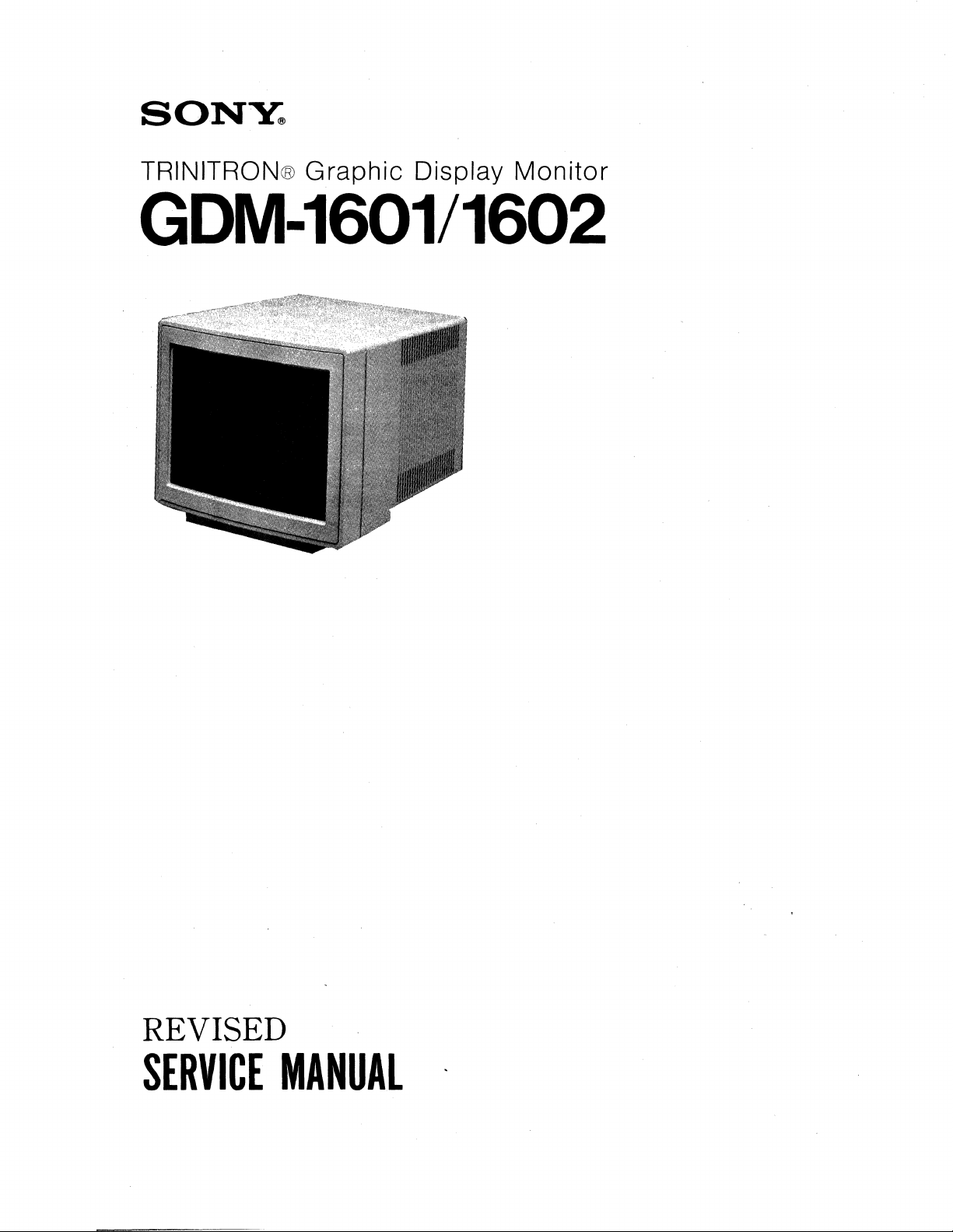
SONY.
TRINITRON®
Graphic
Display
Monitor
GDM-1601/1602
REVISED
SERVICE
MANUAL
:.
(J)"'<''='.:I.
ffl~l3Jr-Jt
~')l.
"'<''='.:I.
7'
)vt:g[,!Jt~
LlL'*To
~:f±(J)~f"iiJttLt:1!nJTl·~~Lt:I).
7'
)v~~fflT
~:. t ~~LI:.
':"ji:.
n l
L'~$~(J)~fFti';I:
~Ut:
gll.sJlI*.i$(tIH'F.
L.
* To
CONFIDENTIAL
i£1:>
I). gll.sJlI*.i$,aUHIV
i*;f~)t~tt~l3Jr-Jl'*
..
~(J)~
The material contained in this manual consists
of
Sony Corporation and
is
intended solely
for
of
use
information
that
by the purchasers
is
the property
of
the equipment described in this manual.
Sony Corporation expressly prohibits the duplication
. or the
use
thereof
for
any purpose other than the operation or maintenance
equipment described in this manual
without
the express written permission
of
any portion
of
this manual
of
of
Sony
Corporation.
CONFIDENTIEL
Le
materiel contenu dans
de
Sony Corporation et sont destinees exclusivement a
I'equipement decrit dans
Sony Corporation
manuel ou
interdit
son
emploi pour
ce
manu.el
ce
manuel.
formellement
tout
consiste
autre
la
but
en
informations qui sont
copie
de
quelque partie que
que
des
operations ou entretiens
I'usage
la
des
acquereurs de
ce
propriete
soit
de
I'equipement a moins d'une permission ecrite de Sony Corporation.
VERTRAULICH
Das
in dieser Anleitung enthaltene Material besteht
tum
der Sony Corporation sind, und ausschlieBlich zum Gebrauch durch den
Kaufer der in dieser Anleitung beschriebenen Ausrustung bestimmt sind.
Die Sony Corporation untersagt ausdrucklich die Vervielfaltigung jeglicher Teile
dieser Anleitung oder den Gebrauch derselben
die Bedienung oder Wartung der in dieser Anleitung beschriebenen Ausrustung
ohne ausdruckliche schriftliche Erlaubnis der Sony Corporation.
aus
I nformationen, die Eigen·
fur
irgendeinen anderen Zweck
the
ce
de
als
SAFETY·RELATED
COMPONENTS
&.
ON THE SCHEMATIC
AND
VIEWS
SAFE OPERATION. REPLACE THESE COMPONENTS
WITH SONY PARTS WHOSE
AS SHOWN
PUBLISHED
THAT
ARE
IDENTIFIED
CEDURES WHENEVER
REPLACED
IDENTIFIED
IN THE PARTS LIST
IN
THIS
BY
CRITICAL
IN THIS
OR
IMPROPER OPERATION
COMPONENT WARNING
BY
SHADING
DIAGRAMS,
ARE
PART
NUMBERS APPEAR
MANUAL
SONY.
MANUAl.
CRITICAL
OR IN SUPPLEMENTS
CIRCUIT
TO SAFE OPERATION ARE
ADJUSTMENTS
FOLLOW THESE PRO·
COMPONENTS ARE
IS
!!
AND
MARK
EXPLODED
CRITICAL
SUSPECTED.
TO
ATTENTION
LES COMPOS ANTS
UNE
PAR
LES VUES EXPLOSEES ET LES LISTES DE PIECES
SONT
SECURITE
PLACER QUE PAR DES COMPOSANTS SONY
NUMERO
MANUEL
SONY. LES REGLAGES DE
TANCE
PRESENT
CRITIQUES,OU
MENT
D'UNE
FONCTIONNEMENT
DE CHAQUE REMPLACEMENT
EST SUSPECTE.
AUX
COMPOSANTS
SECURITE!!
MARQUE
DU
DE PIECE EST
OU DANS DES SUPPLEMENTS PUBLIES PAR
EST
MANUEL.
IDENTIFIES
&SUR
LES SCHEMAS DE PRINCIPE,
IMPORTANCE
FONCTIONNEMENT. NE LES REM-
INDIQUE
CRIT.QUE
LORSQU'UN
POUR
SONT
SUIVRE
RELATIFS A LA
;>AR LINE
CRITIQUE
DANS
CIRCUIT
LA
.IDENTIFIES
CES PROCEDURES LORS
DE
MAUVAIS
TRAME
POUR
DONT
LE PRESENT
DONT
L'IMPOR-
SECURITE DU
DANS LE
COMPOSANTS
FONCTIONNE-
ET
LA
Lt:
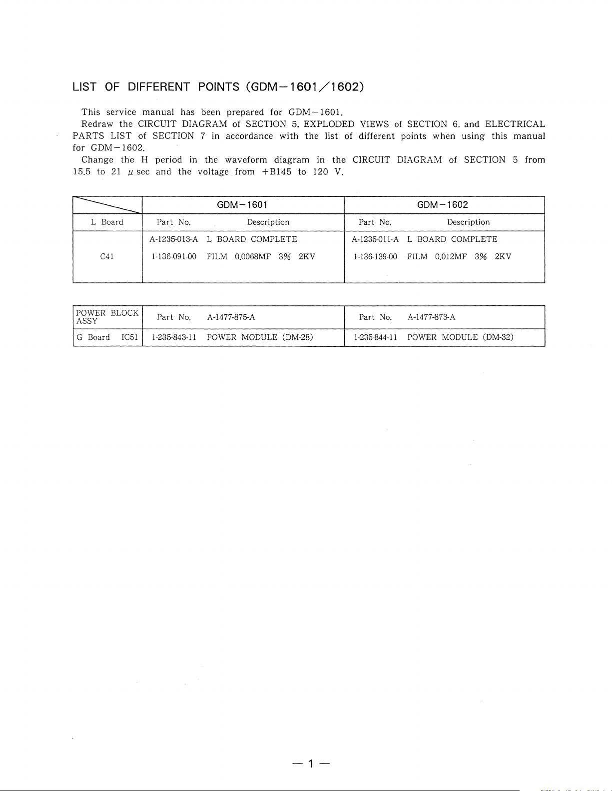
LIST
PARTS LIST of SECTION 7 in accordance
for
15.5
OF
This
service
Redraw
GDM
Change
to
DIFFERENT
manual
the
CIRCUIT DIAGRAM of SECTION 5, EXPLODED
-1602.
the H period
21
/J.
sec
and
POINTS
has
been
in
the
the
voltage from
(GDM
prepared
waveform
+B145
-1601/1602)
for GDM
with
diagram
-160l.
the
list of different points
in
to 120
VIEWS
the
CIRCUIT DIAGRAM of SECTION 5
V.
of SECTION
when
6,
using
and
ELECTRICAL
this
manual
from
L Board
--------
C41
POWER BLOCK
ASSY
G
Board
IC51 1-235-843-11 POWER MODULE (DM-28) 1-235-844-11 POWER MODULE
Part
A-1235-013-A
1-136-091-00
Part
GDM-1601
No. Description
L BOARD COMPLETE A-1235-011-A L BOARD COMPLETE
FILM
0.0068MF
No. A-1477-875-A
2KV 1-136-139-00 FILM 0.012MF
3%
Part
Part
No.
No.
GDM-1602
A-1477-873-A
Description
3%
CDM-32)
2KV
-1-
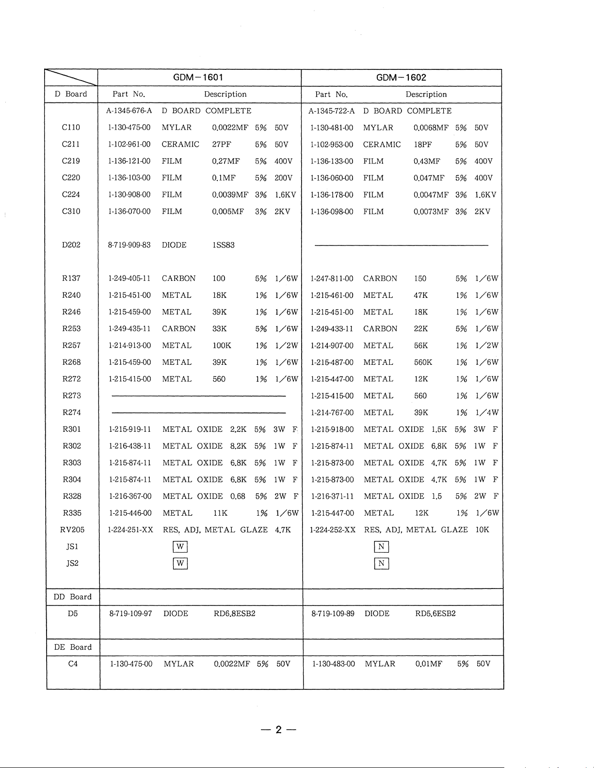
D
Board
-----
C110
C211
C219 1-136-121-00 FILM
C220 1-136-103-00
C224 1-130-908-00 FILM
C310
Part
No.
A-1345-676-A
1-130-475-00
1-102-961-00
1-136-070-00 FILM
GDM-1601
D BOARD
MYLAR
CERAMIC
FILM
Description
COMPLETE
0.0022MF
27PF
0.27MF
O.lMF
0.0039MF
0.005MF
GDM-1602
Part
No. Description
A-1345-722-A
5%
50V
5%
50V
5%
400V 1-136-133-00
200V 1-136-060-00 FILM 0.047MF
5%
3%
1.6KV
2KV 1-136-098-00 FILM
3%
1-130-481-00 MYLAR
1-102-953-00 CERAMIC 18PF
1-136-178-00 FILM 0.0047MF
D BOARD COMPLETE
FILM
0.0068MF 5%
5%
0.43MF
0.0073MF
5%
5%
3%
3%
50V
50V
400V
400V
1.6KV
2KV
D202 8-719-909-83 DIODE
R137 1-249-405-11
R240 1-215-451-00
R246 1-215-459-00
R253 1-249-435-11 CARBON
R257 1-214-913-00
R268 1-215-459-00
R272 1-215-415-00
R273
R274 1-214-767-00
R301 1-215-919-11
R302 1-216-438-11
R303
R304
R328 1-216-367-00
R335
RV205
1-215-874-11
1-215-874-11
1-215-446-00
1-224-251-XX
CARBON 100
METAL
METAL
METAL
METAL
METAL
METAL
METAL
METAL
METAL
METAL
METAL
RES~
AD],
ISS83
18K
39K
33K
lOOK
39K
560
OXIDE 2.2K
OXIDE
OXIDE
OXIDE
OXIDE
11K
METAL
8.2K 5%
6.8K
6.8K 5%
0.68
GLAZE
5%
l/6W
1%
1/6W
1%
1/6W
5%
l/6W
1%
l/2W
1%
l/6W
1%
1/6W
3W F 1-215-918-00
5%
lW
F
1W F
5%
lW
F
2W F 1-216-371-11
5%
1%
l/6W
4.7K
1-247-811-00 CARBON 150
1-215-461-00
1-215-451-00
1-249-433-11 CARBON 22K
1-214-907-00
1-215-487-00
1-215-447-00
1-215-415-00
1-215-874-11
1-215-873-00
1-215-873-00
1-215-447-00
1-224-252-XX
METAL
METAL
METAL
METAL
METAL
METAL
METAL
METAL
METAL
METAL
METAL
METAL
METAL
RES, ADJ,
47K
18K
56K
560K
12K
560 1%
39K 1%
OXIDE
OXIDE
OXIDE
OXIDE
OXIDE
12K 1%
METAL
5%
1%
1%
5%
1%
1%
1%
1.5K
5%
6.8K
5%
4.7K 5%
4.7K 5%
1.5
5%
GLAZE
1/6W
l/6W
1/6W
1/6W
1/2W
1/6W
1/6W
1/6W
1/4W
3W
lW
1W F
lW
2W F
l/6W
10K
F
F
F
JSl
]S2
DD
Board
D5 8-719-109-97 DIODE RD6.8ESB2 8-719-109-89 DIODE RD5.6ESB2
Board
DE
C4 1-130-475-00 MYLAR
~
~
0.0022MF
5%
50V
1-130-483-00 MYLAR O.OIMF 5% 50V
[K]
[K]
-2-
TABLE OF CONTENTS
1. GENERAL
2.
DISASSEMBLY AND REPLACEMENT
3.
CIRCUIT
ADJUSTMENTS
4.
DIAGRAMS
5.
DESCRIPTIONS
6. EXPLODED VIEWS
7. ELECTRICAL PARTS LIST
SECTION
GENERAL
TABLE OF CONTENTS
1
Section
1-1. Features (GDM-1601)
1-2. Specifications
1-3. Features (GDM-1602)
1-4. Specifications (GDM-1602)
1-5. Location
and
Title
.............
(GDM-160l)
.............
Function
of
.........
.........
Controls
....
1-1
1-1
1-2
1-2
1-3
,-,.
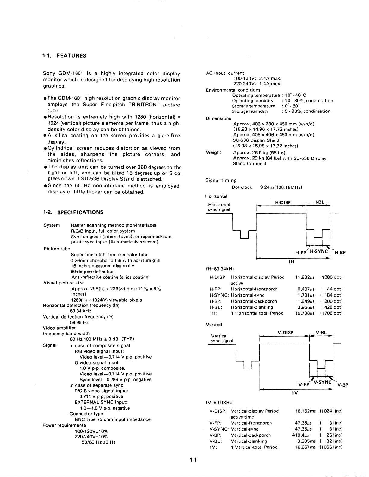
FEATURES
Sony
GDM·1601
monitor
graphics.
•
•
• A
.Cylindrical
•
.Since
'-2.
which
The
GDM-1601
employs
tube.
Resolution
1024
(vertical)
density
display.
the
diminishes
The
fight
grees
display
color
silica
sides,
display
or
down
the
of
SPECIFICATIONS
is
high
the
Super
is
extremely
picture
display
coating
screen
sharpens
reflections.
unit
left,
and
if
SU-536
60
Hz
little
is a highly
designed
resolution
Fine·pitch
elements
can
on
the
reduces
can
be
can
be
Display
non·interlace
flicker
can
for
displaying
high
be
obtained.
screen
distortion
the
turned
tilted
be
integrated
graphic
TRINITRON®
with
per
picture
over
15
Stand
method
obtained.
color
high
resolution
display
1280
(horizontal)
frame,
thus a high·
provides a glare-free
as
viewed
corners,
360
degrees
degrees
is
up
attached.
is
employed,
display
monitor
picture
from
and
to
the
or 5 de-
AC
input
current
100-120V:
220-240V:
Environmental conditions
x
Dimensions
Weight
Signal
Horizontal
. Horizontal
sync signal
Operati
Operating
Storage temperature : 0° -60°
Storage
Approx.
(15.98 x 14.96 x 17.72 inches)
Approx.
SU·536 Display Stand
(15.98 x 15.98 x 17.72 inches)
Approx.
Approx.
Stand (optional)
timing
Dot
clock 9.24ns(108.18MHz)
2AA
max.
1AA
max.
ng
temperature : 10° - 40° C
humidity : 10·80%.
humidity
406
x 380 x 450 mm
406 x 406
26.5
kg
29
kg
1 "
: 5 - 90%. condinsation
x 450 mm
(58 Ibs)
(64
Ibs)
with
H-DISP
condinsation
(w/h/d)
(w/h/d)
SU-536 Display
H-BL
-I"
"I
System Raster scanning method (non·interlace)
Picture tube
Visual picture size
Horizontal
Vertical
Video
frequency band
Signal In case
Power requirements
RIGIB
input,
full
Sync on
posite sync
Super fine·pitch Trinitron color tube
0.26mmphosphor
16
inches measured diagonally
90·degree deflection
Anti-reflective coating (silica coating)
Approx.
inches)
12BO(H)
deflection
63.34 kHz
deflection
59.98 Hz
amplifier
60 Hz·100 MHz ± 3 dB (TYP)
In case
Connector type
)(
frequency (fv)
width
of
RIB video signal input:
Video
G video Signal input:
1.0 V p.p, composite,
Video
Sync
of
RIGIB
video signal input:
0.714 V p.p, positive
EXTERNAL SYNC input:
1.0-4.0
BNC type 75 ohm input .impedance
100-120V±10%
220-240V±10%
50/60
color
green
(internal sync).
input
(Automaticaly selected)
pitch
295(h) x 236(w) mm
1024(V) viewable pixels
frequency (fh)
composite signal
level-O.714
level-0.714
level-0.286
separate sync
V p.p, negative
Hz ±3 Hz
system
or
separated/com.
with
aparture grill
5
(11
/
8
V p.p, positive
V p.p, positive
V p.p, negative
x 9'/s
fH=63.34kHz
H-DISP: Horizontal-display Period
H·FP: Horizontal-frontporch
H-SYNC: Horizontal-sync
H·BP: Horizontal-backporch
H-BL: Horizontal-blanking
H:
1
Vertical
Vertical
sync signal
active
1 Horizontal
total
Period
I.
fV=59.98Hz
V·DISP: Vertical-display Period
time
V-FP: Vertical-frontporch
V-SYNC: Vertical-sync
V-BP: Vertical-backporch
V-BL: Vertical-blanking
V:
1
active
1 Vertical-total Period
1H
11.832}Ls (1280
o A07}Ls
1.701/o1
1.849/015
3.956/015
15.788/015
V-DISP
V-FP
1V
16.162ms (1024 line)
47.35}Ls
47.35/015
41004/015
0.505ms
16.667ms
dot)
44
dot)
184
200
428
(1708
V-BL
3 line)
3 line)
26
32 line)
(1056 line)
dot)
dot)
dot)
dot)
V.BP
line)
s
kt~~
V-SYN~
,-,
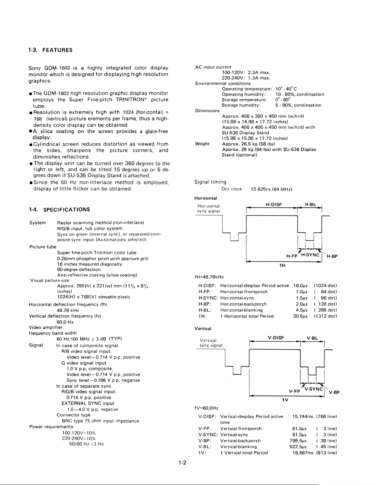
1-3. FEATURES
Sony
monitor
GDM·1602
which is designed for displaying high resolution
is a
highly
integrated color
display
graphics.
• The
GDM·1602
.high resolution graphic display
monitor
employs the Super Fine·pitch TRINITRON" picture
tube.
with
1
024
• Resolution is extremely high
768
(vertical) picture elements per frame, thus a high·
density
.A
color
display
silica coating
on
can
be
obtained.
the
screen provides a glare-free
(horizontal) x
display.
• Cylindrical screen reduces
the
sides,
diminishes
• The display
right
or
grees
down
.Since
display
sharpens
reflections.
unit
left,
the 60
of
can
and
can
if
SU-536 Display Stand
Hz
non·interlace method is employed,
little
flicker
be
be
can
the
turned
distortion
picture
tilted
be
obtained.
as viewed from
over
360
15
degrees
is
attached.
corners, and
degrees
up
to
or
1-4. SPECIFICATIONS
System
Picture
Visual
Horizontal
Vertical
Video
frequency
Signal
Power
Raster
R/G/B
Sync
posite sync
tube
Super
0.26mm
16
inches measured
90-degree
Anti-reflective
picture
size
Approx.
inches)
1024(H) x 768(V)
deflection
48.78
deflection
60.0
amplifier
band
width
60 Hz·100
In
case
RIB
G
In
case
R/G/B
EXTERNAL
Connector
BNC
requirements
100·120V±10%
220·240V
scanning
input,
on
green (internal sync).
fine·pitch
phosphor
295(h)
kHz
frequency
Hz
of
video
Video
video
1.0 V p.p;
Video
Sync
of
video
0.714 V p.p,
1.0-4.0
type
50/60
method
full
color
input
(Automaticaly
Trinitron
pitch
deflection
coating (silica coating)
x 221 (w)
viewable pixels
frequency
(fv)
MHz
± 3
composite
signal
input:
level-0.714
signal
input:
composite,
level-0.714
level-0
..
286 V p.p,
separate
signal
positive
SYNC
V p.p, negative
type
75
ohm
± 1 0%
Hz
±3
Hz
(non·interlace)
system
color
with
diagonally
mm
(fh)
dB
(TYP)
signal
V p.p,
V p.p,
sync
input:
input:
input
impedance
or
separated/com·
selected)
tube
aparture
negative
grill
(11'/. x 8Y.
positive
positive
the
5 de-
1-2
AC
input
current
Environmental
Dimensions
Weight
Signal
timing
Horizontal
Horizontal
sync signal
100·120V:
220·240V:
conditions
Operating
Operating
Storage
Storage
Approx.
(15.98 x 14.96 x 17.72
Approx.
SU-536
(15.98 x 15.98 x 17.72
Approx.
Approx.
Stand
Dot
2.3A
1.3A
temperature:
humidity:
temperature:
humidity:
406 x 380 x 450
406 x 406 x 450
Display Stand
26.5
kg
29
kg
(optional)
clock
15.625ns
I-
,..-----------,
(64
max.
max.
(58
Ibs)
10°·
10
0°.60°
5 - 90%,
inches)
inches)
Ibs)
with
(64
H-DISP
I.
fH=48.78kHz
H-DISP: Horizontal-desplay Period active
H-FP:
H-SYNC:
H-BP:
H-BL:
1
H:
Vertical
Vertical
sync signal
fV=60.0Hz
V-DISP:
V-FP:
V-SYNC:
V-BP:
V-BL:
1V:
Horizontal·frontporch
Horizontal-sync
Horizontal·backporch
Horizontal-blanking
1
Horizontal
Vertical·desplay Period active
time
Vertical-frontporch
Vertical·sync
Vertical-backporch
Vertical·blanking
1
Vertical·total
total
Period
Period
V·DISP
40°C
- 80%,
condinsation
condinsation
mm
(w/h/d)
mm
(w/h/d)
with
SU-536 Display
MHz)
~:tji
H·FP
1H
1V
H·SYN~
16.0J,LS
1.0J,Ls
1.5J,Ls
2.0J,Ls
4.5J,Ls
20.5J,Ls
V·BL
~
V.FP
V-SYNC
15.744ms
61.5J,Ls
61.5J,Ls
799.5J,Ls
922.5J,Ls
16.667ms
(1024
(
64
(
96
(
128
(
288
(1312
(768
39
45
(813
H.BP
dot)
dot)
dot)
dot)
dot)
dot)
V-BP
line)
line)
3
3 line)
line)
line)
linld
1-5.
LOCATION
rr=---~--~-~-.
I I
I I
AND
FUNCTION
OF
CONTROLS
~~~~]
II
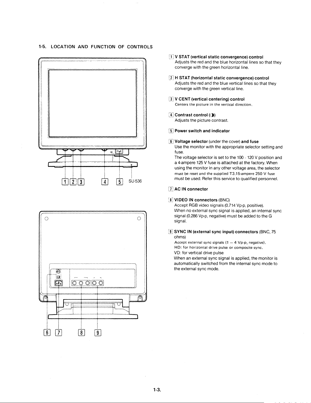
m v STAT (vertical static convergence) control
Adjusts
converge
m H STAT (horizontal static convergence) control
Adjusts the red and the blue vertical lines so
converge
m V CENT (vertical centering) control
Centers
the red and the blue horizontal lines
with
the
green horizontal line.
with
the green vertical line.
the
picture
in
the
vertical
direction.
so
that
that
they
they
I
I
W Contrast control (et)
W Power switch and indicator
L~""""",,
II
I
__
~--
~=""""IJ
W Voltage selector (under the cover) and fuse
/r-
r
WWW
0
~~:
19J
[[;l~
• I
~
~
c ,
~_QJ~
!
4
I I
W
• I
SU-536
II]
[II] VIDEO IN connectors (BNC)
0
[I]
Adjusts
Use the
fuse.
The voltage selector
a 4-ampere 125 V fuse is attached
using
must
must
AC IN connector
Accept RGB video signals (0.714 Vp-p, positive).
When
signal (0.286 Vp-p, negative)
Signal.
SYNC IN (external sync input) connectors (BNC,
ohms)
Accept external sync signals
HD: for horizontal drive pulse
VD: for vertical drive pulse
When an external sync signal is applied, the
automatically
the
the
picture contrast.
monitor
the
be reset
be used. Refer
no
external sync mode.
with
the appropriate selector
is
set
to
the
100 - 120 V position and
at
the factory. When
monitor
external sync signal is applied, an internal sync
in
and
the
switched
any
other
supplied
this
service
from
voltage area,
T3.15-ampere
to
qualified personnel.
must
be added
(1
- 4 Vp-p, negative).
or
composite
the
internal sync
250
to
sync.
setting
the
selector
V fuse
the
monitor
mode
and
G
75
is
to
.~
Ir
I
[I]
~\
!
I
I
7 []]
~
A
l~
1
1-3.
SECTION 2
DISASSEMBLY AND REPLACEMENT
TABLE OF CONTENTS
Section Title
2-1. Rear Cabinet
2-2. Location
2-3. Location
2-4. Location
2-5. Location
2-6. Location
Screen and
2-7. Bezel Removal . . . . . . . . . . . . . . . .
2-8. Control Block Removal . . . . . . . . . .
2-9. Switching Regulator Unit and
Convergence
2-10. Flyback Transformer Assy and
HV Block Removal . . . . . . . . . . . . . 2-6
2-11. Deflection PCB, Video Amp
Arc Suppression
2-12. Picture Tube Removal . . . . . . . . . . .
Removal.
of
Rear Panel
of
Adjustment for A Board 2-2
of
Adjustment for L Board 2-2
of
Adjustment for D Board 2-3
of
Adjustment for Focus,
H. Stat
PCB
PCB
. . . . . . . . . .
............
...............
Removal . . . . . . . .
PCB
and
Removal
.......
..
..
..
..
..
2-1
2-1
2-3
2-4
2-4
2-5
2-7
2-8
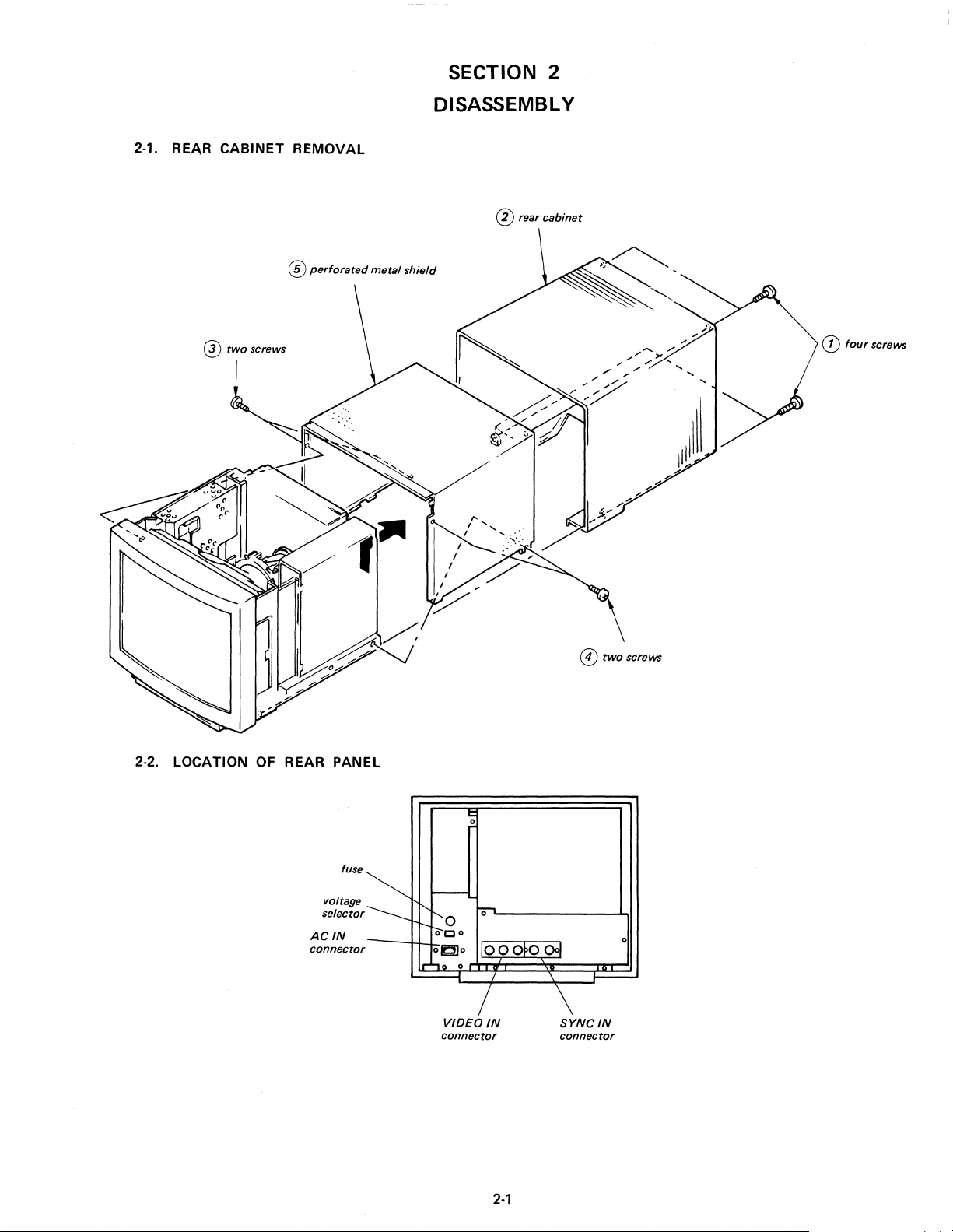
2-1. REAR CABINET REMOVAL
SECTION 2
DISASSEMBL Y
o
two
screws
®
perforated
metal
shield
® rear
cabinet
o
two
screws
o
four
screws
2-2. LOCATION
OF
REAR PANEL
ACIN
connector
fuse
voltage
selector
~
t'-..
r-.f'0
-----
I
...
i---
o
to-c
o~o
'"'"
0
VIDEO
connector
~
fo-o
110001'0001
/
/
IN
2-1
I---
\
SYNC
IN
connector
0
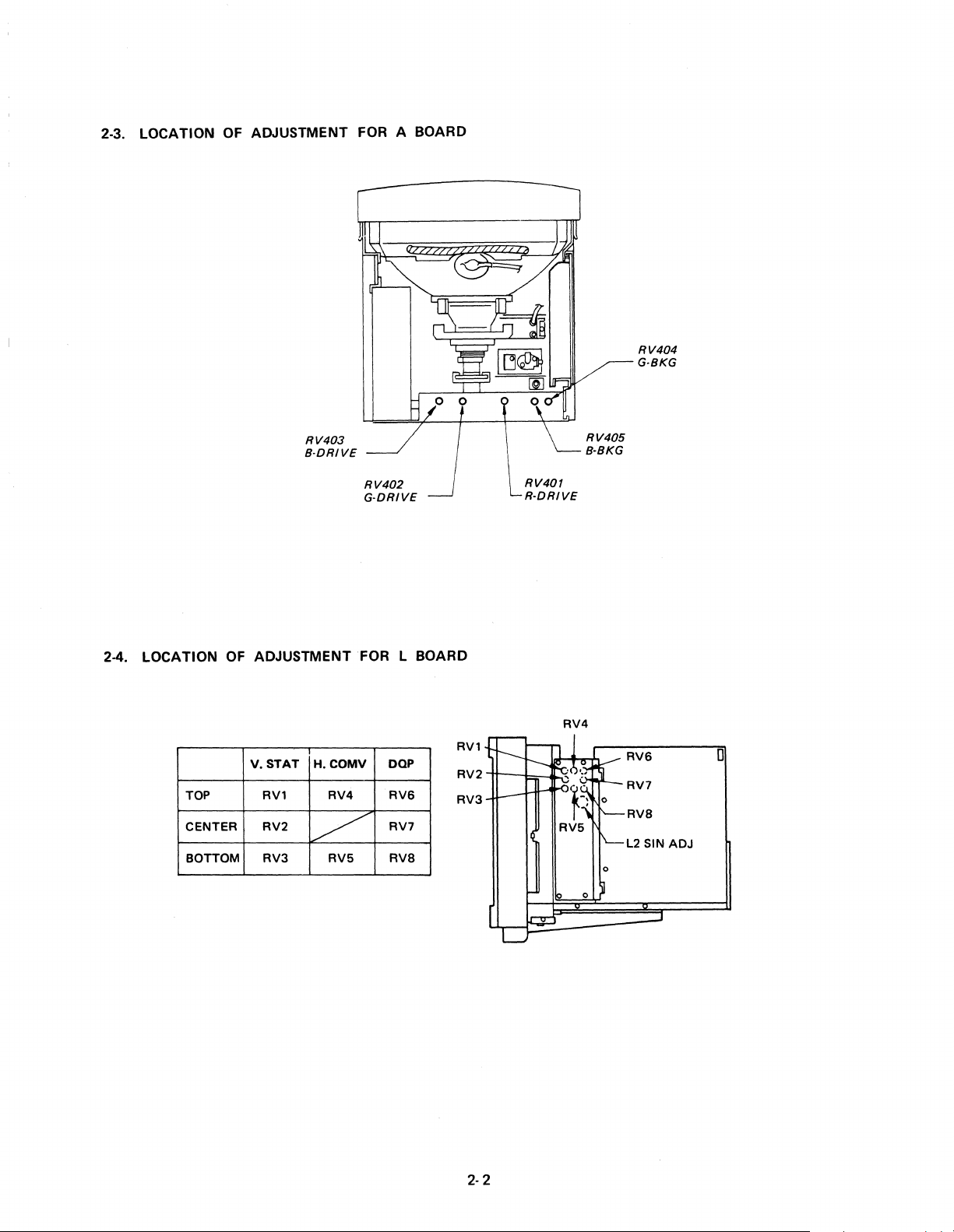
2-3. LOCATION
OF
ADJUSTMENT
FOR
A BOARD
RV404
G·8KG
2-4. LOCATION
TOP
CENTER
BOTTOM
RV403
8·DRIVE
RV402
G·DRIVE
OF
ADJUSTMENT FOR L BOARD
V.STAT
RV1
RV2
RV3
H.COMV
RV4
/
RV5
oap
RVe
RV7
RVa
RV1
RV2
RV3
RV401
R-DRIVE
RV4
RV405
8-8KG
RVe
RV7
RVa
l2
SIN
0
ADJ
2-2
2-5_
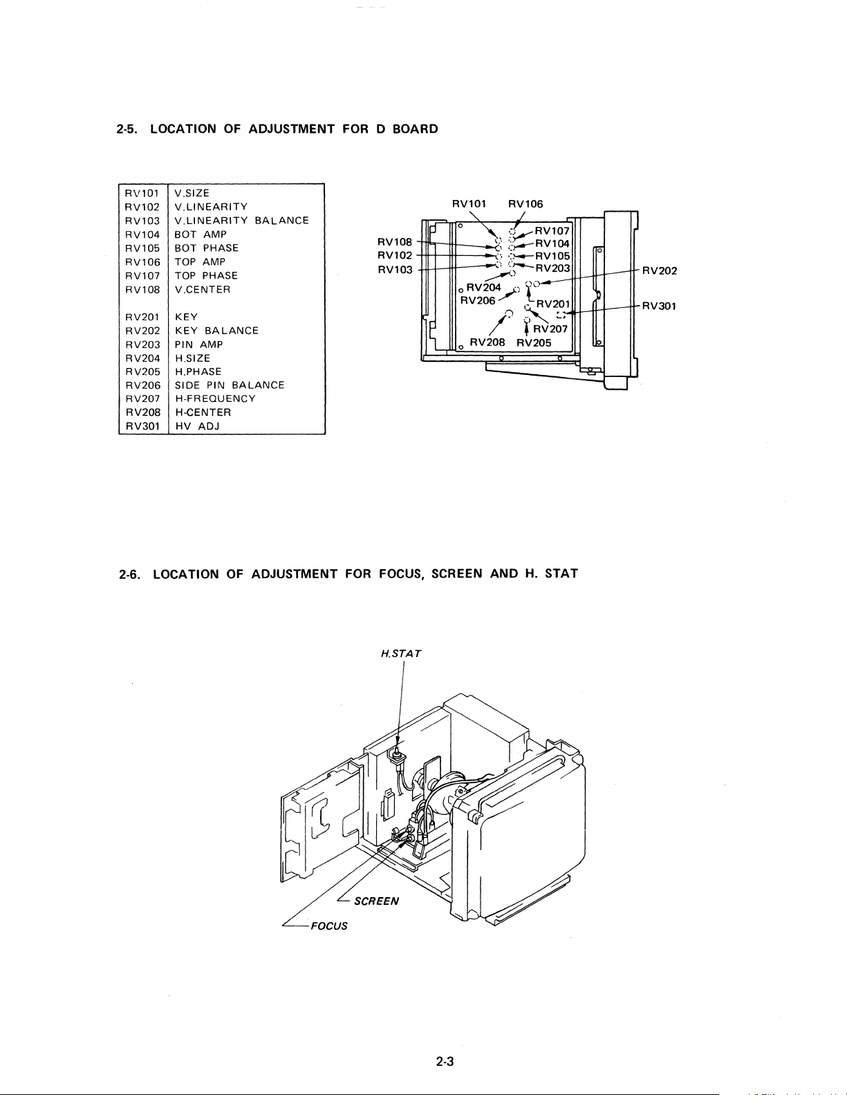
LOCATION
OF
ADJUSTMENT
FOR
D BOARD
RV10l
RV102
RV103
RV104
RV105
RV106
RV107
RV108
RV201
RV202
RV203
RV204
RV205
RV206
RV207
RV208
RV301
V.SIZE
V.LlNEARITY
V.LlNEARITY
BOT
AMP
BOT PHASE
TOP AMP
TOP PHASE
V.CENTER
KEY
KEY
BALANCE
PIN AMP
H.SIZE
H.PHASE
SIDE PIN
H-FREQUENCY
H-CENTER
HV
ADJ
2-6. LOCATION
BALANCE
BALANCE
OF
ADJUSTMENT
FOR
RV108
RV102
RV103
FOCUS,
p
RV10l
0
RV106
"'-
,,\,
~f.yRV107
_
'-;
;::,--RV104
-,;,;
':~RV105
/~RV203
o
RV204
RV206
/'
.~
/_.
o
I~
RV208
SCREEN
AND H. STAT
j
".
~.
....
')(~
~
RV201
-
0
-
D
l)RV2~;
RV205
~
-
-]
::=1
RV202
RV301
1
H.STAT
2-3
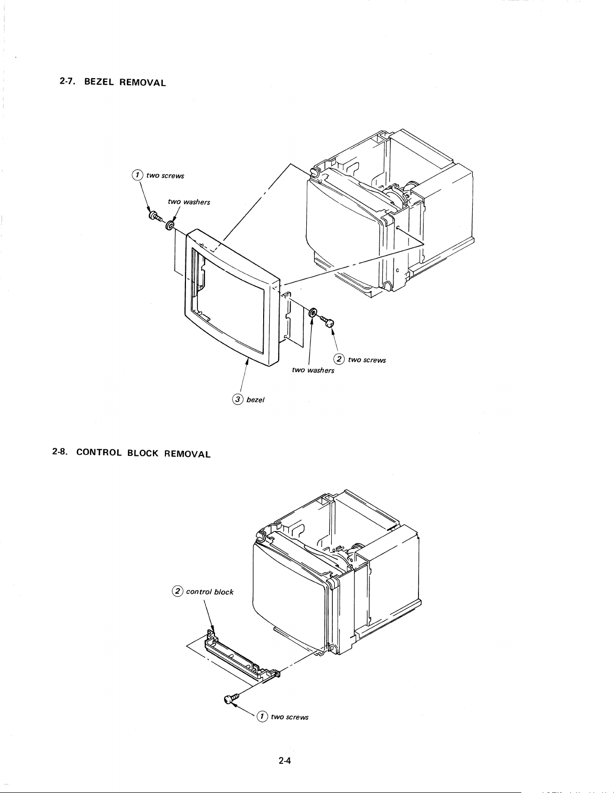
2-7. BEZEL REMOVAL
two washers
2-8. CONTROL BLOCK REMOVAL
o control block
o bezel
(j) two screws
2-4
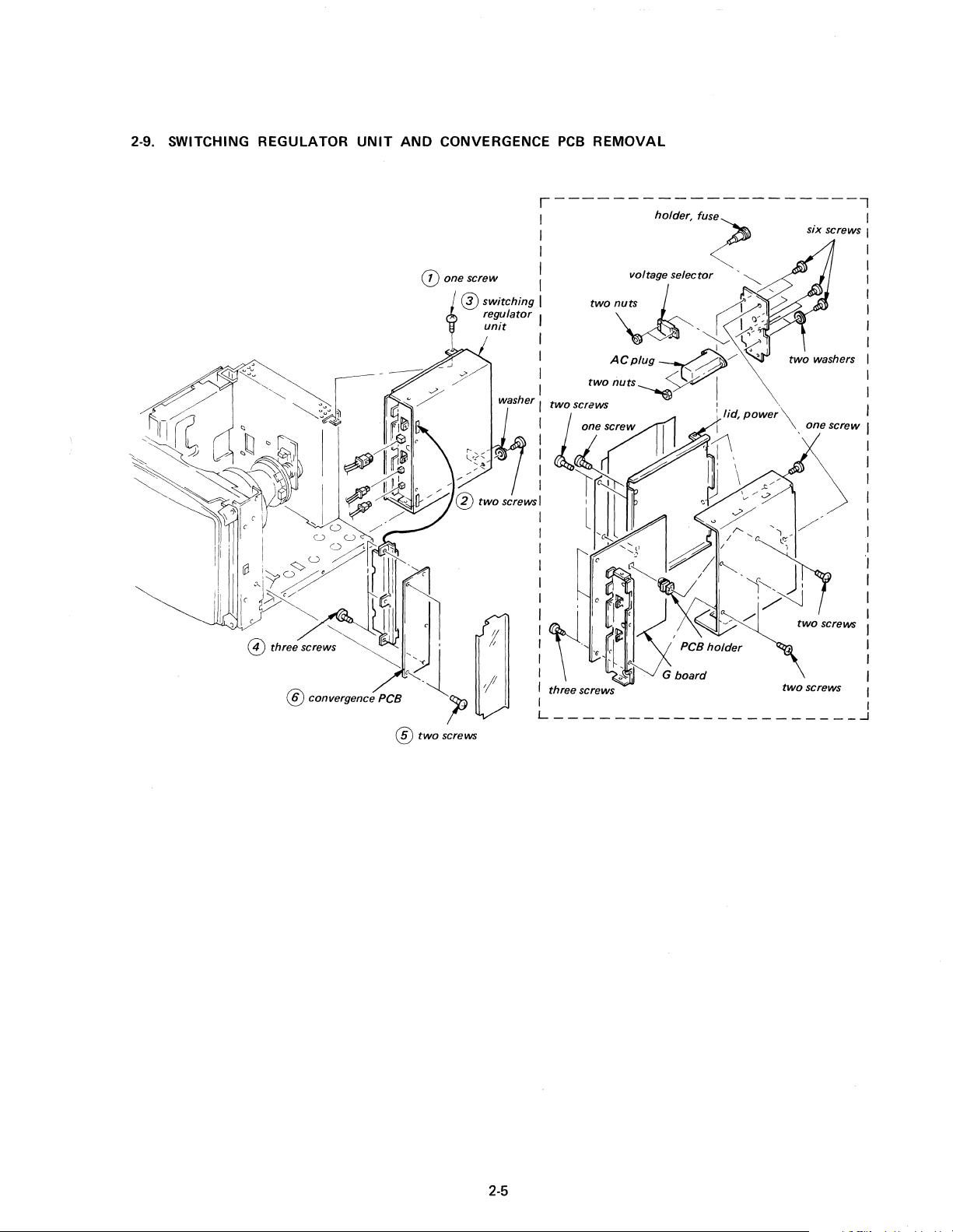
2-9. SWITCHING REGULATOR
UNIT
AND CONVERGENCE
([)
one screw
® switching I
regulator I
unit
PCB
REMOVAL
---,
. I
SIX
screws I
I
I
I
I
two washers I
I
I
I
I
I
I
2-5
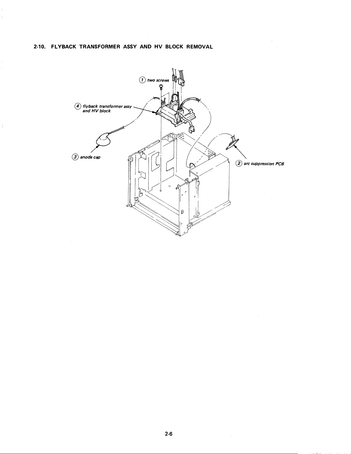
2-10. FL YBACK TRANSFORMER
ASSY
AND
HV
BLOCK
REMOVAL
o flyback transformer
and
HVblock
® anode cap
assy
2·6
2-11.
DEFLECTION
PCB,
VIDEO
AMP
PCB
AND
ARC
SUPPRESSION
PCB
REMOVAL
o
~hield
"A"
(])
two
screws
o deflection
PCB
® video amp
PCB
® three screws
® I/O panel assy
2-7
2-12_
PICTURE TUBE REMOVAL
(j)
anode cap
o
110
(])
three screws
panel
assy
o
four
flange
nuts
• ANODE CAP REMOVAL
o
Turn
up
one
side
indicated
by
the
of
arrow
the
®.
rubber
Anode
cap
button
in
the
direction
o
o
When
one
anode
button,
up
the
arrow@).
Using a
direction
side
rubber
of
the
cap
thumb,
indicated
the
rubber
anode
and
pulling
pull
by
cap
cap can
up
up
the
it
is
be
in
the
rubber
arrow@.
separated
removed
the
direction
by
cap
from
turning
of
firmly
the
the
in
the
2-8
SECTION 3
CIRCUIT DESCRIPTIONS
TABLE OF CONTENTS
Section
3-1. A Board . . . . . . . . . . . . . . . . . . . .
3-li-l. Composition . . . . . . . . . . . . . . .
3-1:-2.
Contrast Amplifier (AA Board) . . .
3-1-3. Pedestal Clamp (AA Board)
3-14.
Sync Separator and Pulse Generator
(AB Board) . . . . . . . . . . . . . . . .
3-1-5. Video
3-1-6. Blanking
3-2. B Board
3-3. C Board
3-4. D Board (Deflection and
HV Regulation)
3-4-1. DA Board . . . . . . . . . . . . . . . . .
34-2.
34-3.
3-44.
3-4-5. Vertical Deflection
3-4-6. Blanking Pulse
3-4-7. HV Regulator
Output
Amplifier.
......................
......................
DB Board
DC Board . . . . . . . . . . . . . . . . .
Horizontal Deflection
Circuit
'"
Title
Amplifier.
. . . . . . . . . .
...
. . . . . . . . . . . .
...
. . . . . . . . . . . . . .
Output
.................
Output
Generator.
................
.......
. . . . . . .
. . . . . .
. . . . . .
..
..
..
..
..
..
..
..
..
..
, 3-3
..
..
3-1
3-1
3-1
3-1
3-1
3-1
3-2
3-2
3-2
3-2
3-2
3-2
3-2
34
34
3-4
Section Title
3-4-8. HV Hold-Down Circuit
3-4-9. Beam
34-10.
3-5. G Board (Power Supply)
3-5-1.
3-5-2.
3-5-3. Degauss
3-54.
3-5-5.
3-6. H Board
3-7.
J Board
3-8. L Board
3-8-1. Composition '
3-8-2. Modulated Waveform Generator
3-8-3. Horizontal Convergence
3-84.
3-8-5. Dynamic Quadrapole (DQP) Drive . . .
Protector
Scan Failure
AC
Line Filter
AC
Voltage Selector
...................
OVP Circuit
DC
Power Supply (Regulator)
.....................
......................
.....................
Vertical Convergence
..............
Protection
...............
...........
.................
................
...........
.........
..........
.....
...
.........
3-5
.
3-5
.
3-5
.
3-5
.
3-5
.
3-5
.
3-5
.
3-5
.
3-5
3-6
.
.
3-6
3-6
.
.
3-6
3-6
.
.
3-6
.
3-6
3-6
3-1_
A BOARD
3-1-1. Composition
The A board consists
amplifiers
pedestal clamp circuit,
blanking circuit. In
and
on
the
mounted
fier and clamp circuit. The
on
the
c'ontrol pulse generators.
3-'
-2. Contrast Amplifier (AA Board)
The
amplifier for
circuit
tracking
fier gain can be
ment
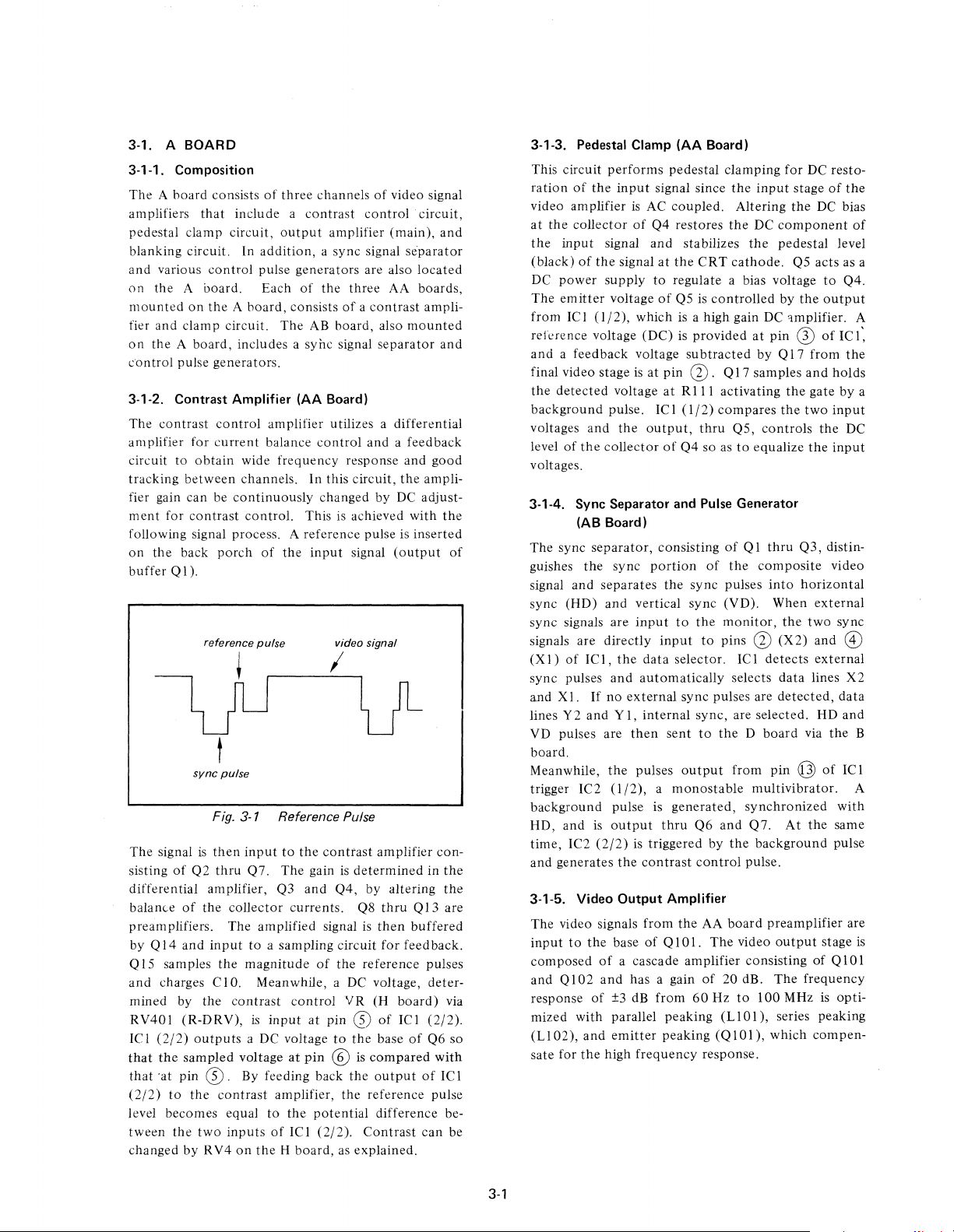
following signal process. A reference pulse is inserted
on
the
buffer
that
various
contrast
control
A board. Each
on
the
A board, includes a sync signal
control
current
to
obtain
between
for
contrast
back
QI).
of
three
channels
include a
A board, consists
wide frequency response and
channels.
continuously
control.
porch
contrast
output
addition,
pulse generators are also
of
AB
amplifier utilizes a differential
balance
of
control
In
This is achieved with
the
input
control
amplifier (main),
a sync signal
the three AA boards,
of a contrast
board, also
and a feedback
this circuit,
changed by
signal
video signal
of
video signal
separator
located
mounted
separator
the
DC
(output
circuit,
and
ampli-
and
good
ampli-
adjust-
the
of
I
t
sync
pulse
Fig. 3-1 Reference Pulse
The signal
sisting
differential amplifier, Q3
balance
preamplifiers. The amplified signal is
by
QI4
15
Q
and
mined by the
RV401
IC I (2/2)
that
that
(2/2)
level becomes equal
tween
changed
is
then
input
to
the
conttast
of
Q2
thru
Q7. The gain
and
of
the collector currents. Q8
and
input
to
a sampling circuit for feedback.
samples
charges C I
the
'at pin G). By feeding back
to
(R-DRV),
outputs
sampled
the
the
two
by
RV4
the
magnitude
O.
Meanwhile, a
contrast
is
a DC voltage
voltage
contrast
inputs
on
the
of
control
input
at
pin
to
at
pin ® is
amplifier,
to
the
potential
of
IC I
(2/2).
H board, as explained.
amplifier con-
is
determined
Q4, by altering
thru
Q 13 are
then
buffered
the
reference pulses
DC
voltage, deter-
VR
(H
board)
G)
of
IC1
the
base
of
compared
the
output
the
reference pulse
difference be-
Contrast
of
can
in
the
the
via
(2/2).
Q6 so
with
ICI
be
3-'
-3. Pedestal Clamp (AA Board)
This circuit
ration
video amplifier
at
the
the
(black)
power
DC
The
emitter
from
reference voltage (DC) is
and
a feedback voltage
final video stage
the
detected
background
voltages
level
voltages.
performs
of
the
collector
input
signal
of
the
supply
IC I (1/2),
and
of
the
collector
pedestal clamping for DC resto-
input
signal since
is
AC coupled. Altering
of
Q4 restores
and
stabilizes
signal
at
the
CRT
to
regulate a bias voltage
voltage
pulse. IC 1
of
Q5 is
which is a high gain
provided
subtracted
is
at pin
(}).
voltage
the
at
RIl1
output,
of
Q4
(1/2)
thru
the
the
the
cathode.
controlled
Q 17 samples
activating
compares
Q5,
so as
to
input
DC
component
pedestal level
by
DC
'lmplifier. A
at
pin ® of
by
QI7
the
the
controls
equalize
3-1-4. Sync Separator and Pulse Generator
(AB
Board)
The sync
guishes
signal
sync (HD)
sync signals are
signals are directly
(X
sync pulses
and
lines Y2
VD pulses are
board.
Meanwhile,
trigger IC2
background
HD, and
time, IC2
and generates
3-'-5.
The video signals
input
composed
and Q I
response
mized
(Ll
sate for
I)
02),
and
of
XI.
to
separator,
the
separates
and
IC 1,
and
If
no
and Y I,
the
(1/2), a monostable
is
output
(2/2)
Video
the
of
02
and
of
±3 dB
with
parallel
and
the
high
consisting
sync
portion
vertical
input
the
data
automatically
external
internal
then
pulses
pulse is
is triggered by
the
contrast
Output
from
base
of
a cascade amplifier consisting
has a gain
from
emitter
frequency
of
the
sync pulses
sync
to
the
input
to
selector.
sync pulses are
sync,
sent
to
output
generated,
thru
Q6
control
Amplifier
the
AA
QI01.
The
of
60
Hz
peaking
peaking (Q I 0
response.
of
QI
thru
the
composite
into
(VD). When
monitor,
pins
selects data lines X2
are selected. HD
the D board
from
and
the
board
20
(Ll 0 I),
the
(})
(X2)
IC I detects
detected,
pin @ of
multivibrator.
synchronized
Q7.
At
background
pulse.
preamplifier are
video
output
dB.
The
to
100 MHz is
series peaking
I),
which
stage
of
the
the
DC
bias
of
Q5 acts as a
to
Q4.
the
output
IC
from
the
and
holds
gate
by
two
input
the
DC
the
input
Q3,
distin-
video
horizontal
external
two
sync
and ®
external
data
and
via
the
IC
with
the
same
pulse
stage
of
Q I 0 I
frequency
opti-
compen-
1:
a
B
I
A
is
3-1
3-1-6. Blanking Amplifier
Blanking signals are
B
board,
to
the
is
switched
of
approximately
Q404.
specific
G 1 grids
clamping levels can be varied by
RV40S (B-BKG),
for
background
3-2. B BOARD
The B board
the
A board
All signal
to
suppress
Q 1 acts as a fade
monitor
turned
a
minimum.
switched
to
the
3-3. C BOARD
The C board
to
the
mounted
are
charge (flash-over)
3-4. D
3-4-1.
The
horizontal
vertical
are processed
The
from
and
phase by a
circuit. Meanwhile,
a voltage divider
and
delayed H sync
compared
AFC
with
delay
horizontal
deflection
The
signal
puts
pin
Ii§>
off
The
DC
levels
of
the
and
I/O,
RFI.
is
powered
on
and
off,
normal
relays
CRT
electrodes.
BOARD
DA
Board
DA
board
phase
synchronization
horizontal
the A board,
Q]
of
IC
PHASE
triggers a SAW
in
circuit synchronizes
the
HD
signal. RV20S (H-PHASE)
time
of
position
is
driven
vertical oscillator
and
locked
two
vertical rate pulses, a V drive pulse from
and
a V blanking pulse from pin
input
from
base
of
Q403
when
Q403
is
60
Vp-p appears
blanking pulses are
and
supplied
CRT
via
the
C board.
with
respect
level
adjustment.
is an
interface
the
as well as
control
up. When
clamps
C2 is gradually charged up
returning
level.
the
on
the
current
(Deflection
performs
locked
and
controlled
and
vertical sync (HD, VD) signals
positive
1.
The
SHIFTER
the
(C22S,
signal
the
AFC
the
PHASE
of
by
at a frequency
card
D, H, and power
DC
power
for
the
contrast
the
contrast
bias voltages and video signals
Spark
board
to
chassis
the
loop,
functions. These
by
true,
H sync signal
horizontal
C226),
TOOTH
and
the
circuit. The
the
SHIFTER
the
display image.
the
output
is
triggered by
the
D board, via
to
switch
it
on, and a blanking pulse
at
the
then
clamped
to
each
of
Two
RV404
to
the
power
gaps
to
return
and
horizontal
vertical oscillator,
IC
are
and is
is
GENERATOR.
(G-BKG)
the
Red channel,
for signals
supply
I/O,
contain
picture
is applied,
control
control
and
neon
the
ground.
HV
Regulation)
I.
input
to
is
then
input
to
retrace pulse,
fed back
sawtooth
horizontal
at
of
to
output
controls
and
adjusts
Horizontal
pin 0 .
the
60
Hz. IC 1
Qj)
the
on.
Q404
emitter
individual
when
voltage
and
oscillator,
functions
delayed in
of
at
the
three
and
between
boards.
filters
the
Ql
to
Q 1
voltage
lamps
CRT
dis-
and
pins
CD
an AFC
thru
pin ®
The
wave are
from
the
scanning
the
the
VD sync
out-
.
is
is
DB
3-4-2.
The
tooth
ICI
a vertical
capacitor
sawtooth
tor
and
diodes D 1
sawtooth
circuit via
Miller
period
output
tion
output
is
input
correction.
component
allow
at
the
the V -sawtooth
other
3-4-3.
The
from
board
Th~
positive and negative
are varied
IC I
waves
and
forms a similar
the
Meanwhile,
triggers a phase
after
Q4
phase shift is varied by
(j)
ments
correction.
(1/2)
switch
ingly, a
Q4,
sawtooth
inverted by IC2
Board
DB
board
generates waveforms, including a saw-
wave, for S-correction
(1/2),
configured
period
sawtooth
C2
control
wave.
The
bias
is
supplied from IC2
the
peaks
of
the
and
DS. The resulting zero-crossing
wave
is
input
RVIOI
integrator,
parabolic wave. IC 1
from IC2
wave (similar
is
amplitude
to
adjustment
top
and
correction
DC
Board
DC
board
T203
and generates a
sawtooth
by
(l
/2)
to
modulate
bottom
starting
passing
of
ICI
for
both
is
input
QS
activated
horizontal
is
generated
wave
(V-SIZE)
IC2
(1/2)
to
adjusted
the
vertical deflection circuit for linearity
RVI03
to
(HOT)
sums
pincushion
point
the
(2/2)
The
(V-LINE BALAj\lCE) adds a
the V sawtooth
of
the
bottom
and
circuits
receives
and
complex
is
input
RV104,
the
the
function
of
H retrace pulse is inverted by Q 1 and
control
thru
Q2.
and allows individual phase adjust-
top
and
output
to
Miller
by
sawtooth
and
output
(1/2)
and
half
is
of
vertical deflection.
as a Miller
the
(2/2)
waveform are
(I/2),
and
a sine wave)
balance
of
V -sine waves are supplied
on
the
the
to
RVIOS,
amplitude
horizontal
correction.
for phase
the
shifter
the
bottom
voltage from pin
integrator
the
amplitude
from IC 1
is
integrator,
wave. Transistor Q 1
rise
and
fall times
current
to
Dl,
waves,
The
of
the
ramp
to
pin @
the
and
also
generates a vertical
(2/2)
generates an S-correc-
by
RVI02
wave
the
display. Additionally,
the
D board.
horizontal
V-sawtooth
"butterfly"
02,
and
RVI06,
tamp
horizontal
composed
magnitude
output
pincushion
of
determined
vertical
of
and D3, split
adjusted
control
deflection
input
to
integrates
at
pin (j). This
(V-LIN)
at
IC2
vertical linearity
retrace pulse
from
waveform.
the
amplitudes
and
signals for
ICl
(2/2)
by altering
ramp signals.
of
of
voltage from pin
distortion
sawtooth
CD
IC2
(2/2)
with
collector
signal,
input
of
Q4.
synchronized
modulated
(1/2).
This signal
to
QI03.
generates
of
genera-
ICI
another
(1/2)
the
RVI07.
Q3 and
the pulse
of
Accord-
by the
and
the
(1/2)
by
the
and
DC
to
to
DB
into
top
per-
IC 1
reset
by
is
3-2
 Loading...