

Sony Trinitron CPD-E530, CPD-G520P Service Manual
CHASSIS
SERVICE MANUAL
SPECIFICATIONS
CPD-E530
CR1
AEP Model
Chassis No. SCC-L33T-A
TRINITRON
®
COLOR GRAPHIC DISPLAY
CRT
0.24 mm aperture grille pitch, 90-degree deflection, FD Trinitron
21 inches measured diagonally
Viewable image size
Approx. 403.8 × 302.2 mm (w/h) (16 × 12 inches)
19.8" viewing image
Resolution (H:Horizontal, V:Vertical)
Maximum: H: 2048 dots, V: 1536 lines
Recommended: H: 1600 dots, V: 1200 lines
Input signal levels
Video signal: Analog RGB: 0.700 Vp-p (positive), 75 Ω
SYNC signal: H/V separate or composite sync:
TTL 2 kΩ, Polarity free
Sync on Green: 0.3 Vp-p (negative)
Standard image area
Approx. 388 × 291 mm
(15 3/8 × 11 1/2 inches) or
Approx. 364 × 291 mm
(14 3/8 × 11 1/2 inches)
Deflection frequency*
(H:Horizontal, V:Vertical)
H: 30 to 117 kHz, V: 48 to 170 Hz
AC input voltage/current
100 to 240 V, 50 – 60 Hz, 2.0 – 1.0 A
Power Consumption
Approx. 135 W
Operating temperature
10 ºC to 40 ºC
Dimensions Approx. 497 × 502 × 485 mm (w/h/d)
(19 5/8 × 19 × 18 7/8 inches)
Mass Approx. 30 kg (66 lb 2 oz)
Plug and Play DDC2B/DDC2Bi, GTF**
* Recommended horizontal and vertical timing condition
• Horizontal sync width duty should be more than 4.8% of total
horizontal time or 0.8 µs, whichever is larger.
• Horizontal blanking width should be more than 2.3 µsec.
• Vertical blanking width should be more than 450 µsec.
** If the input signal is Generalized Timing Formula (GTF) compliant, the
GTF feature of the monitor will automatically provide an optimal
image for the screen.
CPD-E530 (E) 2
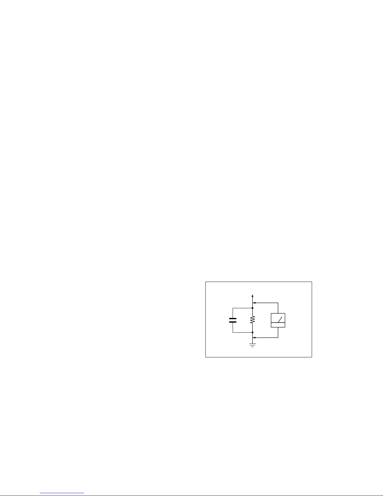
LEAKAGE TEST
The AC leakage from any exposed metal part to earth ground and from all
exposed metal parts to any exposed metal part having a return to chassis,
must not exceed 0.5 mA (500 microamperes).
Leakage current can be measured by any one of three methods.
1. A commercial leakage tester, such as the Simpson 229 or RCA WT540A. Follow the manufacturers’ instructions to use these instruments.
2. A battery-operated AC milliammeter. The Data Precision 245 digital
multimeter is suitable for this job.
3. Measuring the voltage drop across a resistor by means of a VOM or
battery-operated AC voltmeter. The “limit” indication is 0.75 V, so
analog meters must have an accurate low-voltage scale. The Simpson 250
and Sanwa SH-63Trd are examples of a passive VOMs that are suitable.
Nearly all battery operated digital multimeters that have a 2 V AC range
are suitable. (See Fig. A)
After correcting the original service problem, perform the following safety
checks before releasing the set to the customer:
1. Check the area of your repair for unsoldered or poorly-soldered
connections. Check the entire board surface for solder splashes and
bridges.
2. Check the interboard wiring to ensure that no wires are “pinched” or
contact high-wattage resistors.
3. Check that all control knobs, shields, covers, ground straps, and
mounting hardware have been replaced. Be absolutely certain that you
have replaced all the insulators.
4. Look for unauthorized replacement parts, particularly transistors, that
were installed during a previous repair. Point them out to the customer
and recommend their replacement.
5. Look for parts which, though functioning, show obvious signs of
deterioration. Point them out to the customer and recommend their
replacement.
6. Check the line cords for cracks and abrasion. Recommend the
replacement of any such line cord to the customer.
7. Check the B+ and HV to see if they are specified values. Make sure your
instruments are accurate; be suspicious of your HV meter if sets always
have low HV.
8. Check the antenna terminals, metal trim, “metallized” knobs, screws, and
all other exposed metal parts for AC Leakage. Check leakage as
described below.
Fig. A. Using an AC voltmeter to check AC leakage.
1.5 k
Ω
0.15 µF
AC
Voltmeter
(0.75 V)
To Exposed Metal
Parts on Set
Earth Ground
SAFETY CHECK-OUT

CPD-E530 (E) 3
WARNING!!
NEVER TURN ON THE POWER IN A CONDITION IN WHICH THE
DEGAUSS COIL HAS BEEN REMOVED.
SAFETY-RELATED COMPONENT WARNING!!
COMPONENTS IDENTIFIED BY SHADING AND MARK ¡ ON THE
SCHEMATIC DIAGRAMS, EXPLODED VIEWS AND IN THE
PARTS LIST ARE CRITICAL FOR SAFE OPERATION. REPLACE
THESE COMPONENTS WITH SONY PARTS WHOSE PART
NUMBERS APPEAR AS SHOWN IN THIS MANUAL OR IN
SUPPLEMENTS PUBLISHED BY SONY. CIRCUIT ADJUSTMENTS THAT ARE CRITICAL FOR SAFE OPERATION ARE
IDENTIFIED IN THIS MANUAL. FOLLOW THESE PROCEDURES
WHENEVER CRITICAL COMPONENTS ARE REPLACED OR IMPROPER OPERATION IS SUSPECTED.
CPD-E530 (E) 4
POWER SAVING FUNCTION
This monitor meets the power-saving guidelines set by VESA, ENERGY STAR, and
NUTEK. If no signal is input to the monitor from your computer, the monitor will auto-
matically reduce power consumption as shown below.
Power mode Power consumption ! (power)
indicator
normal operation ≤ 135 W green
active off*
1
≤ 3 W orange
(deep sleep)*
2
power off Approx. 0 W off
* 1When your computer enters power saving mode, NO SIGNAL appears on the screen.
After a few seconds, the monitor enters power saving mode.
* 2“Deep sleep” is power saving mode defined by the Environmental Protection Agency.
Design and specifications are subject to change without notice.
CPD-E530 (E) 5
DIAGNOSIS
Aging Mode (Video Aging) : During Power Save, press MENU button for longer than 2 second.
Self Test (OSD Color Bar) : During Power Save, push up Control button for longer than 2 second.
Reliability Check Mode : During Power Save, push down Control button for longer than 2 second.
Failre
+B failure
Horizontal / Vertical Deflection
failure, Thermal protector
ABL protector
HV failure
Aging / Self Test
Out of scan range
Power LED
Amber → Off
(0.5 sec) (0.5 sec)
Amber → Off
(1.5 sec) (0.5 sec)
Amber → Off
(0.5 sec) (1.5 sec)
Amber → Off → Amber → Off
(0.25 sec) (0.25 sec) (0.25 sec) (1.25 sec)
Amber → Off → Green → Off
(0.5 sec) (0.5 sec) (0.5 sec) (0.5 sec)
Green (OSD indication)
CPD-E530 (E) 6
MODE AT PRODUCTION
MODE 1 MODE 2
RESOLUTION
640 X 480 1600 X 1200
CLOCK
25.175 MHz 229.500 MHz
— HORIZONTAL —
H-FREQ
31.469 kHz 106.250 kHz
usec usec
H. TOTAL
31.778 9.412
H. BLK
6.356 2.440
H. FP
0.636 0.279
H. SYNC
3.813 0.837
H. BP
1.907 1.325
H. ACTIV
25.422 6.972
— VERTICAL —
V. FREQ (HZ)
59.940 Hz 85.000 Hz
lines lines
V. TOTAL
525 1250
V. BLK
45 50
V. FP
10 1
V. SYNC
23
V. BP
33 46
V. ACTIV
480 1200
— SYNC —
INT(G)
NO NO
EXT (H/V) /POLARITY
YES N/N YES P/P
EXT (CS) /POLARITY
NO NO
INT/NON INT
NON INT NON INT
TIMING SPECIFICATION
2001.11.15 VER.

CPD-E530 (E) 7
TABLE OF CONTENTS
Section Title Page Section Title Page
1. DISASSEMBLY
1-1. Cabinet Removal ................................................ 1-1
1-2. A1 Board (C BLOCK) Removal ........................ 1-2
1-3. A1 Board Removal ............................................. 1-3
1-4. Bezel Assembly, H1 Board Removal ................. 1-4
1-5. D Board Removal ............................................... 1-5
1-6. Service Position................................................... 1-6
1-7. Picture Tube Removal......................................... 1-7
1-8. Harness Location ................................................ 1-9
2. SAFETY RELATED ADJUSTMENT ............... 2-1
3. ADJUSTMENTS ...................................................... 3-1
4. DIAGRAMS
4-1. Block Diagrams................................................... 4-1
4-2. Frame Schematic Diagram .................................. 4-4
4-3. Circuit Boards Location ...................................... 4-5
4-4. Schematic Diagrams and Printed Wiring
Boards ................................................................. 4-6
(1) Schematic Diagram of A1 Board ....................... 4-8
(2) Schematic Diagrams of D ( a, b, c) Board .. 4-10
(3) Schematic Diagram of DA Board ...................... 4-14
(4) Schematic Diagram of H1 Board ....................... 4-16
(5) Schematic Diagram of L2 Board ........................ 4-18
(6) Schematic Diagram of N Board .......................... 4-20
4-5. Semiconductors .................................................. 4-22
5. EXPLODED VIEWS .............................................. 5-1
5-1. Chassis ............................................................... 5-2
5-2. Picture Tube ...................................................... 5-3
5-3. Packing Materials................................................ 5-4
6. ELECTRICAL PARTS LIST ............................... 6-1
CPD-E530 (E) 1-1
SECTION 1
DISASSEMBLY
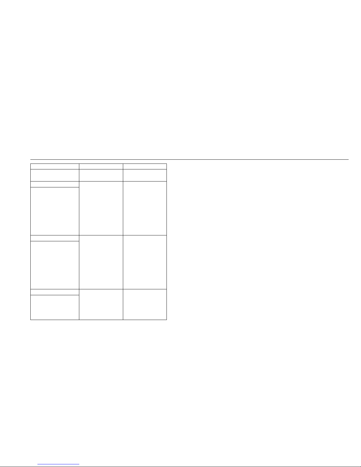
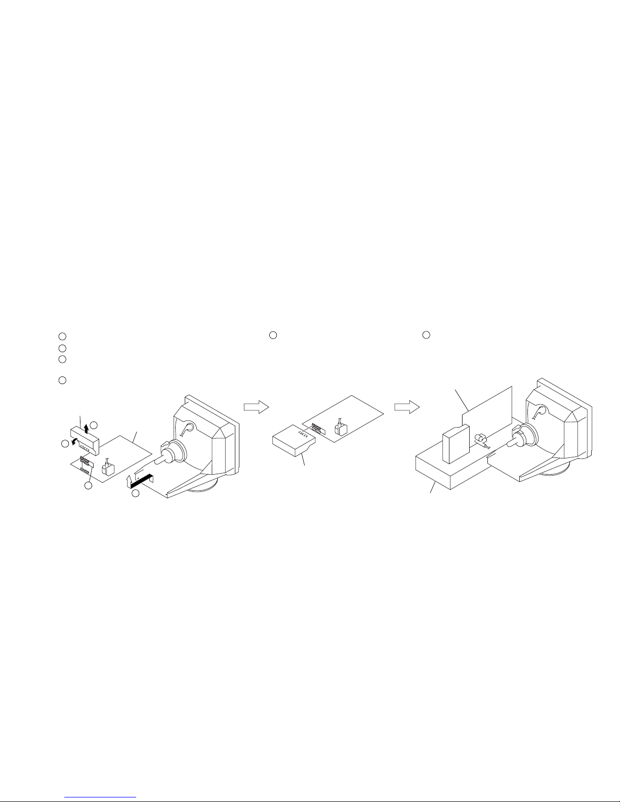
1-1. CABINET REMOVAL
1
Two screws
(+BVTP 4 x 16)
6
Slide the EMI shield in the direction
of arrow C and remove four claws.
7
EMI shield
4
Three screws
(+BVTT 4 x 8)
5
Three screws
(+BVTT 4 x 8)
2
Two claws
Bezel assembly
Bezel assembly
EMI shield
Cabinet
Cabinet
Push in the tip of a screwdriver
about 10mm to unlock the claw.
B
A
C
3
Push the upper side of the cabinet
in the direction of arrow A, disconnect claws,
then remove the cabinet
lifting it up in the direction of arrow B.
CPD-E530 (E) 1-2
1-2. A1 BOARD (C BLOCK) REMOVAL
1
A1 board (C BLOCK)
CN315
CN318
GND
GND
CPD-E530 (E) 1-3
1-3. A1 BOARD REMOVAL
1
Two screws
(+BVTP 3 x 8)
2
Video block assembly
3
Four screws
(+BVTP 3 x 8)
4
Video shield
5
Four screws (HEX)
6
Screw
(+BVTP 3 X 8)
7
Video case
8
A1 board
CN315

CPD-E530 (E) 1-4
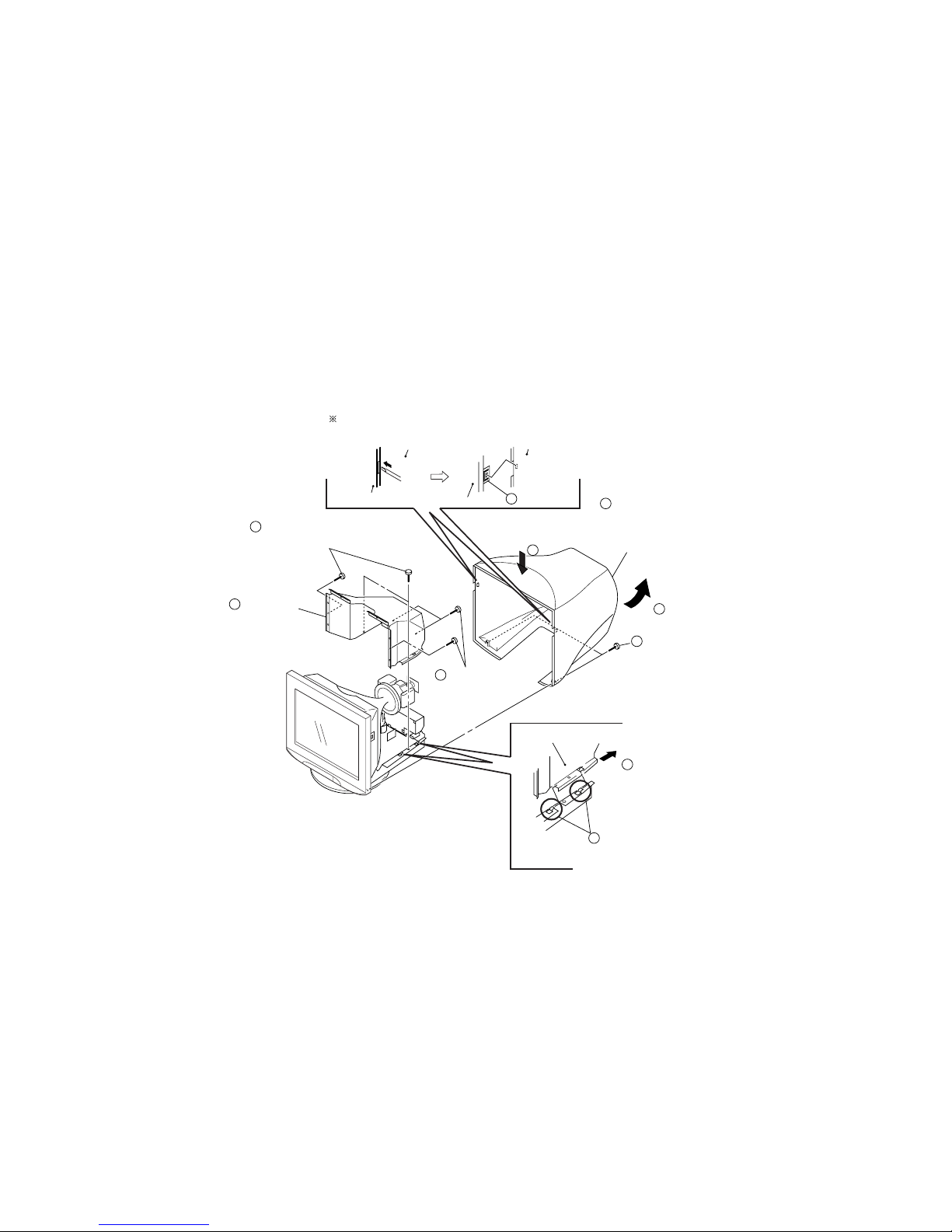
1-4. BEZEL ASSEMBLY, H1 BOARD REMOVAL
2
1
Four tapping screws (5)
5
Bezel assembly
3
Screw
(+BVTP 4 x 16)
4
Screw
(+BVTP 4 x 16)
6
Three screws
(+BVTP 3 x 10)
10
Two claws
H1 board
7
Input selector
button
8
Joy stick
12
Magnetic
MIU-221D sensor
11
L1 blacket
CN1400
CN1500
CN1401
Picture tube shield
Before removing the bezel assembly, secure
the picture tube by attaching two screws to
the picture tube shield at the positions shown
with an arrow (diagonal two places) to prevent
the picture tube from falling.
(Use the screws +BVTT 4 x 8 that fix EMI shield.)
9

CPD-E530 (E) 1-5
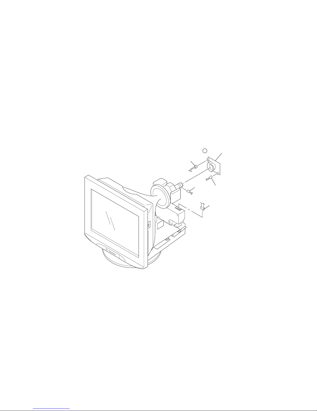
1-5. D BOARD REMOVAL
1
A1 board
(C block)
2
Two screws
(+BVTP 3 x 8)
4
Two screws
(+BVTP 3 x 10)
D board
3
Video block assembly
5
Rear plate assembly
6
Five screws
(+BVTP 3 x 10)
CN315
CN602
CN601
CN1103
CN1601
CN1600
CN1003
CN605
CN701
Connector (4P)
Connector (4P)
CN501
GND
GND
8
Screw (+BVTP 3X10)
7
CPD-E530 (E) 1-6
1
2
4
1
Remove the D board.
D board
2
Remove the Video block assembly.
3
Install the Adaptor board
(XT MOUNT) (A-1391-123-A).
4
Lay the Video block assembly.
Video block assembly
Video block assembly
5
Install the video block assembly.
6
Put a box which is about 15cm in height
under the D board to fix it.
(Please disconnect the CN 701 first.)
D board
Box
3
1-6. SERVICE POSITION

CPD-E530 (E) 1-7
1-7. PICTURE TUBE REMOVAL
4
Picture tube
1
Anode cap (Refer to 1-8)
2
A1 board (C block)
3
Neck assembly
CN1
CN2
CN3
CN2
GND
CPD-E530 (E) 1-8
3When one side of the rubber cap is
separated from the anode button, the
anode-cap can be removed by turning up
the rubber cap and pulling up it in the
direction of the arrow c.
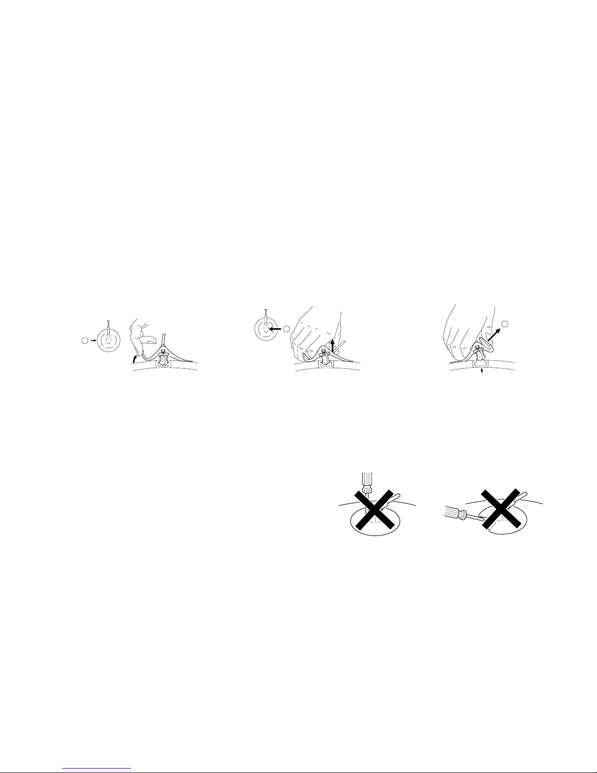
•HOW TO HANDLE AN ANODE-CAP
1Don’t scratch the surface of anode-caps with sharp shaped
material!
2Don’t press the rubber hardly not to damage inside of anode-
caps!
A material fitting called as shatter-hook terminal is built in the
rubber.
3Don’t turn the foot of rubber over hardly!
The shatter-hook terminal will stick out or damage the rubber.
•REMOVAL OF ANODE-CAP
NOTE: Short circuit the anode of the picture tube and the anode cap to the metal chassis, CRT shield or carbon painted on the CRT, after
removing the anode.
•REMOVING PROCEDURES
1Turn up one side of the rubber cap in the
direction indicated by the arrow a.
2Using a thumb pull up the rubber cap
firmly in the direction indicated by the
arrow b.
a
b
c
Anode Button
CPD-E530 (E) 1-9
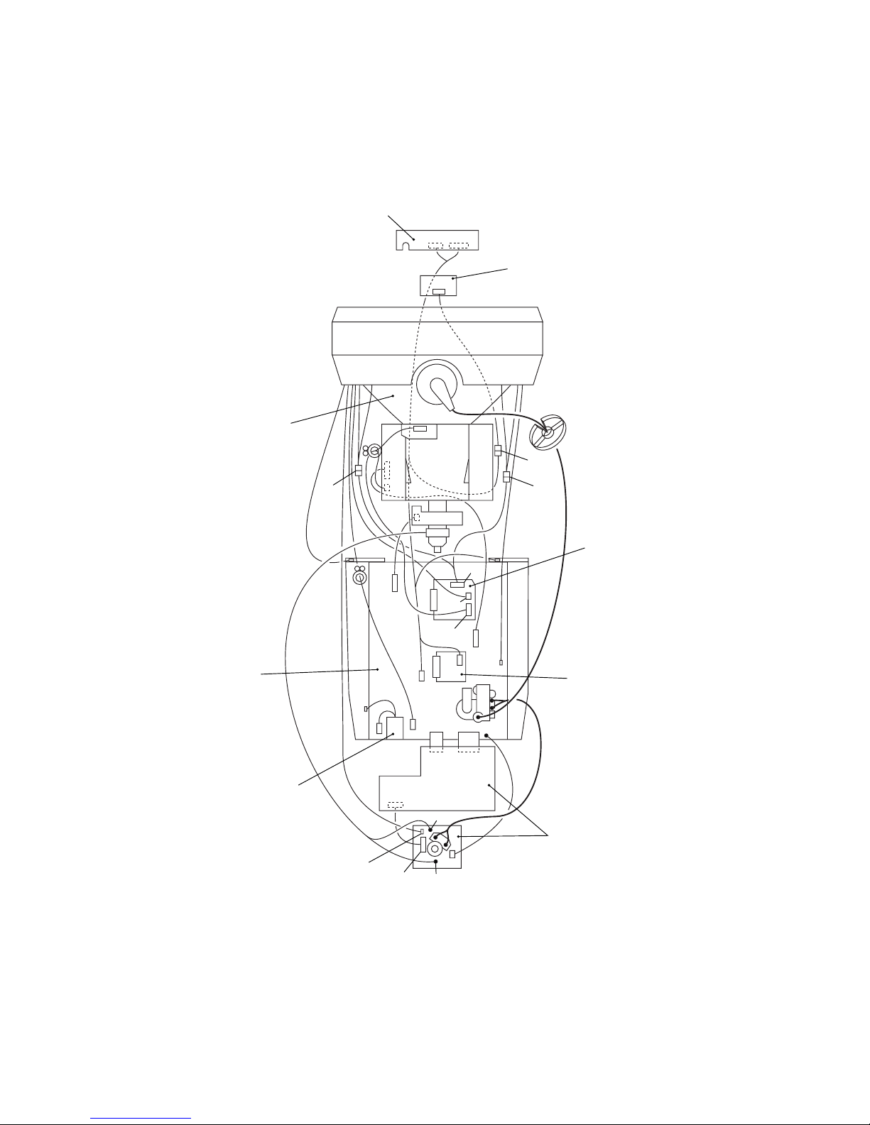
1-8. HARNESS LOCATION
CN602
CN601
CN604 CN1102
CN312 CN311
CN318
CN319
CN320
CN316
CN315
CN303
CN1103
CN1400
CN1500
CN1401
CN701
CN501
CN1601
CN1600
CN1602
CN2
CN1
CN1
5P
CN3
CN1003
CN904
4P
4P
D board
A1 board
N board
L2 board
Magnetic sensor
H1 board
Picture tube
AC inlet (3P)
CPD-E530 (E) 2-1
SECTION 2
SAFETY RELATED ADJUSTMENT
HV Regulator
Circuit Check
HV Protector
Circuit Check
When replacing or repairing the shown below table, the
following operational checks must be performed as a
safety precaution against X-rays emissions from the unit.
Part Replaced ([)
RV901
HV ADJ
* Confirm one minute after turning on the power.
a) HV Regulator Circuit Check
1) Turn the RV901 slowly, and adjustment so that high
voltage is in the specified range.
[Specification]: 27.00 ± 0.05 kV
2) Check that the voltage of D912 cathode on the D
board is 17.0 V or more.
b) HV Protector Circuit Check
1) Using external DC Power Supply, apply the voltage
shown below between cathode of D912 and GND,
and check that the RASTER disappers.
[Specification]: 19.95 + 0.00/– 0.05 V
Part Replaced (])
D Board C925, IC901, R901,
R902, R905, R924,
R925, R926, RV901,
T901 (FBT)
• Mounted D Board
D Board C920, C923, D911,
D912, R903, R917,
R918, R919, R920,
R923, T901 (FBT)
• Mounted D Board
N Board IC1001, RB1001
• Mounted N Board
Beam Current
Protector Circuit
Check
Part Replaced (])
D Board C930, D917, R921,
R932, R933, R935,
T901 (FBT)
• Mounted D Board
N Board IC1001, RB1001
• Mounted N Board

CPD-E530 (E) 2-2
c) Beam Current Protector Circuit Check
1) Connect constant current source to a section between
T901 (FBT) qa pin and GND, and check that the
RASTER disappers when the specified current flows
to the qa pin.
[Specification]: 2.12 + 0.00/– 0.01 mA

CPD-E530 (E) 3-1
SECTION 3
ADJUSTMENTS
Note:Hand degauss must be used on stand-by or power-off condition.
This model has an automatic earth magnetism correction function by using an earth magnetism sensor and a LCC coil. When
using a hand degauss while monitor (LCC coil) is being operated, it sometimes gets magnetized, and the system may not
work properly as a result.
•Landing Rough Adjustment
1. Display all white pattern (or black dot pattern).
2. Set contrast to 255.
3. Display green plain pattern.
4. Side back DY and roughly adjust green plain pattern to be centered on
the useful screen with Purity Magnet.
5. Adjust DY tilt.
Note:Set ROTATION to 128 and LCC_NS to 128 when adjusting DY tilt.
6. Lightly tighten the DY screw.
•Landing Fine Adjustment
Note: (1) After adjust W/B (9300k), measure the average of IK with all
white video input, while CONTRAST is maximum and
BRIGHTNESS is center. And adjustment shall be made so that the
miss-landing become least after aging 2H with the IK 30% of
measured value shown above.
(2) The magnetic field shall be BH = 0.
(3) When adjusting at other than BH = 0, calculate the shifted value
from BH = 0.
1. Put the monitor in helmholz coil.
2. Set as follows;
LCC_SW = 0 (LCC Correction Current = 0)
FUNCTION_SW bit1 = (Auto Degauss = On)
CONTRAST = 255
3. Display green plain pattern.
4. Degauss the iron part of chassis with a hand degausser and degauss coil.
5. Degauss CRT face with a hand degausser again.
6. Input AC 230V to AC IN and turn the monitor off and on. Then autodegauss works.
7. Reset FUNCTION_SW bit1 to 0 (auto-degauss = off)
8. Degauss CRT face with a hand degausser again.
9. Attach wobbling coil to the specified place on CRT neck.
10. Put on landing sensor to CRT face.
11. Set LCC_SW to 12.
12. With landing checker, adjust DY position, purity, DY center and
landing of the 4 corners.
13. Read VX and VY value which are the read out of magnetic sensor, and
write to "LCC_VX_REF" and "LCC_VY_REF".

CPD-E530 (E) 3-2
a
b
cd
<How to place wedge>
Green plain crosshatch pattern
a and b should be equal.
c and d should be equal.
Plaster RTV to both sides for the upper wedge.
Make sure that they settle inside DY.
Plaster RTV to one side for other wedges.
± 6 ± 6 ± 6
± 6 ± 6 ± 6
± 6 ± 6 ± 6
(µm)
10 10 10
10 7 10
10 10 10
(µm)
The red and blue must be within the
specification given right with respect to the
green.
A difference between red and blue must be
within the specification given right.
<Specifications>
Adjust so that the green is within the
specification given right.
4 corner adjust target : within ± 1
0 ± 3 0 ± 7.5 0 ± 3
0 ± 3 0 ± 7.5 0 ± 3
0 ± 3 0 ± 7.5 0 ± 3
(µm)
14. Adjust landing by LCC_NS, LCC_LT, LCC_LB, LCC_RT, and
LCC_RB. Adjustment of registers shall be limited within the following
range.
LCC_NS: 128 ± 15
LCC_LT, LCC_LB, LCC_RT, and LCC_RB: 128 ± 40
Set LCC_SW to 13, and Perform Service Save.
15. Tighten DY screw within specified torque, and auto-degauss.
Note: Torque 22 ± 2 kgcm (2.2 ± 0.2Nm)
16. Adjust the vertical angle of DY to make top and bottom pins equal (a =
b). The horizontal angle shall not be changed (straight). Settle DY
upright without leaning, and insert wedges firmly so that DY shall not
move.
17. Adjust top and bottom pins correction VR.
18. Adjust the horizontal trapezoid distortion by DY horizontal trapezoid
correction VR.
19. Check landing at each corner and in case not in specification, adjust
landing of 4 corners with "LCC_NS", "LCC_LT", "LCC_LB",
"LCC_RT", and "LCC_RB". The limitations of registers are shown
below.
LCC_NS: 128 ± 15
LCC_LT, LCC_LB, LCC_RT, and LCC_RB: 128 ± 40
20. Remove the sensor and wobbling coil.
21. Switch signals to R, G, and B, and then check that the pure colors have
good color purity.
22. Fix purity magnets with white paint.
CPD-E530 (E) 3-3
IBM AT Computer
as a Jig
1-690-391-211A-1500-819-A
Interface Unit
2
*The parts above ( ) are necessary for DAS adjustment.
1
3
D-sub
(9 Pin [female])
mini Din
(8Pin)
4 Pin
3-702-691-01
Connector Attachment
3
To BUS CONNECTOR
4 Pin 4 Pin
•Convergence Specification
B
A
A
0.20 mm
B
0.24 mm
V
XBVXCV
B
R
B
R
R
B
B
R
R
BBR
TLV
TLH
YBHYCH
R B
R B
H.TRAP
TB-PIN
TLH
XCV
Purity
4-pole magnet
6-pole magnet
2-pole magnet
Connect the communication cable of the computer to the connector located on the D board. Run the service software and then follow the instruction.
•Convergence Rough Adjustment
(1) Display white crosshatch pattern.
(2) Pile the convex parts of 6-pole magnet for convergence together.
(3) Roughly adjust H.CONV and V.CONV with 4-pole magnet.
CPD-E530 (E) 3-4
B
a
a 1.8 mm
b 1.8 mm
a
b
b
A
MODE
A
B
4 : 3
388
291
Focus 1
Focus 2
FBT
•White Balance Adjustment Specification
1. 9300 K
x = 0.283 ± 0.005
y = 0.298 ± 0.005
(All White)
2. 6500 K
x = 0.313 ± 0.005
y = 0.329 ± 0.005
(All White)
3. 5000 K
x = 0.346 ± 0.005
y = 0.359 ± 0.005
(All White)
•Vertical and Horizontal Position and Size
Specification
•Focus adjustment
Adjust the focus volume 1 and 2 for the optimum focus.
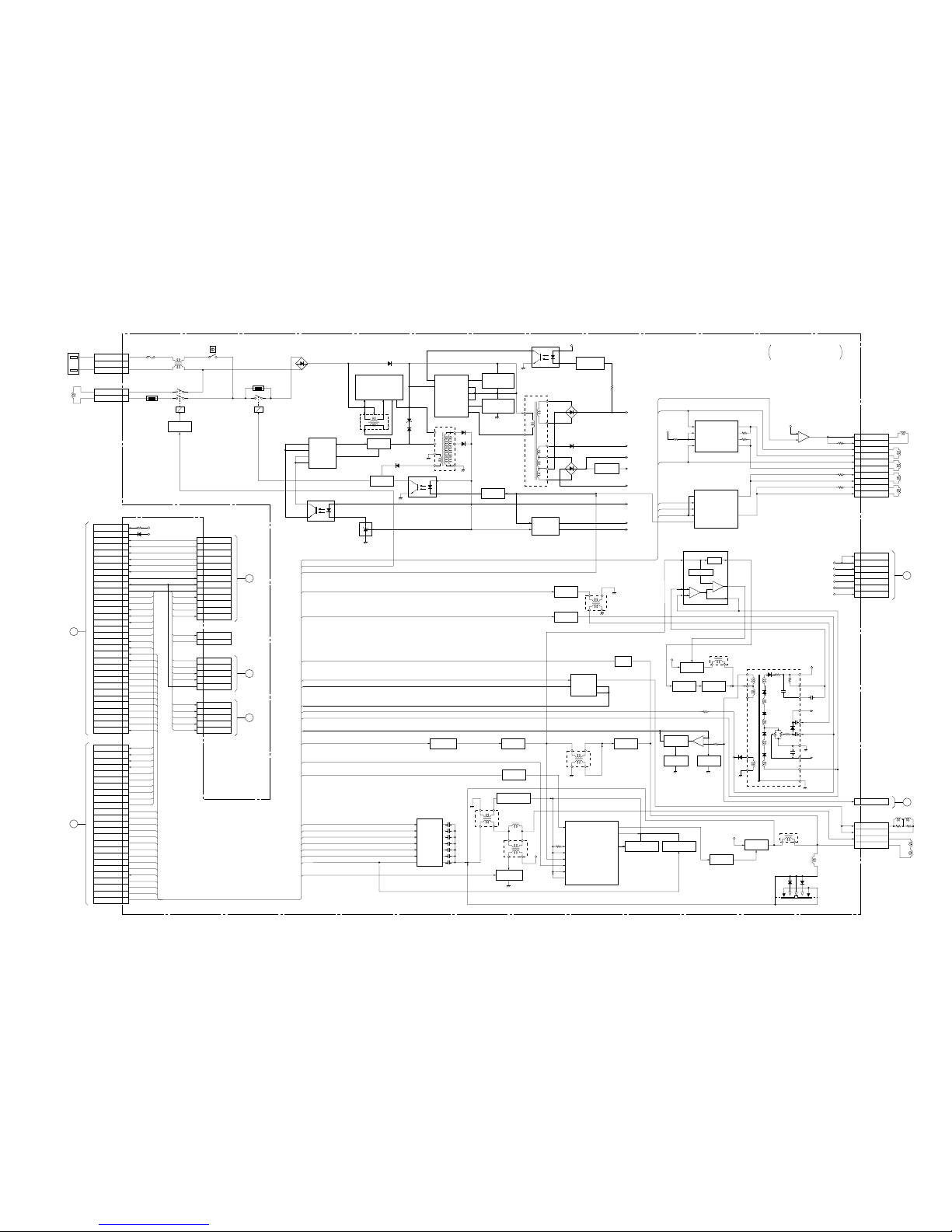
CPD-E530 (E) 4-1
SECTION 4
DIAGRAMS
4-1. BLOCK DIAGRAMS
LED DRIVE
Q1400
D1400
A
G
LED DRIVE
Q1401
A
TO D BOARD
CN1102
2
4
6
7
8
25
28
31
22
23
24
23
22
10
12
14
15
16
B1
G1
R1
V1
H1
OSD R
OSD G
OSD B
OSD BLK
V_DET
BLK
CLAMP
H OUT
V OUT
G.SYNC
R OUT
G OUT
B OUT
26
28
30
8
9
11
7
4
2
R OUT
G OUT
B OUT
5
3
1
R OUT
G OUT
B OUT
R IN
G IN
B IN
R IN
G IN
B IN
COF R
COF G
COF B
SCL
SDA
B2
G2
R2
V2
H2
13
22
23
SW
SCL
SDA
CN307
HD15
5
4
3
2
1
10
15
9
14
8
13
7
12
6
11
CN309
HD15
5
4
3
2
1
10
15
9
14
8
13
7
12
6
11
IC003
OSD
IC008
INPUT SELECT
IC001
RGB PRE-AMP
IC002
RGB AMP
15 14 13 12
18 20 19 21
12 11 10
14
3
5
7
4
5
2
32
31
30
4
3
12
13
27
23
24
25
15
14
13
ROUT
GOUT
BOUT
SOG
SYNC IN
RCI
GCI
BCI
XTAL IN
HS OUT
VS OUT
ECO SW
SCL
SDA
HS OUT
VS OUT
ECO SW
SCL
SDA
SCL
SDA
HS OUT
VS OUT
ECO SW
CS IN
VS IN
HS IN
RIN
GIN
BIN
IC004
CUT OFF AMP
IC011
HEATER REG
X001
24.5MHz
18 19 21
H FLY
OSD R
OSD G
OSD B
OSD BLK
AV
BLK
CLP
BUFFER
Q101,
Q201,
Q301
1
2
4
6
7
8
9
+B
+B
+80V
+12V
7V
3.3V
5V
+B
+80V
+12V
7V
3.3V
5V
CN312
G2
1
G2
CN318
5
3
1
7
KR
KG
KB
HEATER+
CN315
5
3
1
7
KR
KG
KB
HEATER+
FVFCHV
CN318
V901
PICTURE TUBE
7
101718
11
10
2
C
TO D BOARD
CN604
TO D BOARD
FBT
A1
(VIDEO AMP, RGB OUT)
H1
(USER CONTROL)
L2
(CY, LCC)
R_IK
G_IK
B_IK
B-SS3602<AEP>-BD1-EPS05
Vcc OUT
VADJ
7V
10
11
9
7
8
6
1
4
15
16
2
3
13
DDC SCL1
DDC SDA1
DDC GND1
DDC SCL2
DDC SDA2
DDC GND2
H BLK
INPUT SW
IIC SCL
IIC SDA
HS OUT
VS OUT
ECO SW
CN311
1 2 13 12
IC006
INVERTER
IC007
ROM
3 4 11 10
9856
SDA
SCL
VCLK
5
6
7
IC009
ROM
SDA
SCL
VCLK
5
6
7
2
3
4
5
8
12
13
14
WAKE UP
KEY SCAN
LED1
LED2
INPUT SW
T_AMB
VY
VX
CN1400
CN1401
D
TO D BOARD
CN1103
E
TO N BOARD
CN1003
TO MAGNETIC
SENSOR UNIT
4
5
6
7
8
GXSC
GYSC
LCC NS
IIC SDA
IIC SCL
CN1603
F
TO D BOARD
CN1106
B
KEY DET
Q1402
S1403
3
2
VX
VY
5V
5V
INPUT1
INPUT2
IC1603
4
2
1
+
–
2
1
4
3
21
20
IC1602
DAC
SDA
SCL
AO2
AO1
AO4
AO3
LCC-NS
12LCC-NS (+)
LCC-NS (–)
CN1600
1
2
3
4
5
6
7
8
LCC-LT (+)
LCC-LT (–)
LCC-LB (+)
LCC-LB (–)
LCC-RT (+)
LCC-RT (–)
LCC-RB (+)
LCC-RB (–)
CN1602
LCC-LT
LCC-LB
LCC-RT
LCC-RB
IC1601
(1/2)
2
3
4
+
–
IC1601
(2/2)
8
7
6
+
–
IC1600
(1/2)
2
3
4
+
–
IC1600
(2/2)
8
7
6
+
–
IC1604
(1/2)
2
3
4
+
–
IC1604
(2/2)
8
7
6
+
–
3
4
1
2
CY4+
CY4–
CY3+
CY3–
CN1601
TH1400
24
IC005
INVERTER
SW
Q004
SW
Q005
SW
Q002
SW
Q001
S1402
CONTROL
S1401
PICTURE
EFECT
S1400
MENU
1
2
CPD-E530 (E) 4-2
B-SS3602<AEP>-BD2-EPS05
G
TO D BOARD
CN502
1
33
37
34
36
15
11
13
7
20
19
22
24
16
21
23
2
38
39
40
32
35
5
12
10
H.DF
REFDC
XDC
HD OUT
HFBP
H BLK
VS OUT
HS OUT
PLL LOCK
IIC SDA
IIC SCL
LCC_NS
HSAW_SW
H.LINBAL
GYSC
GXSC
V.DF
D.TILT
YSC
XSC
HSHAPE
YDC
POC
DCC2
VSAWN
CN1101
CN1001
CN1003
7
5
6
+
–
2
3
4
+
–
IC1102
AMP
DA
(DPU)
N
(
µ-COM
)
I
TO D BOARD
CN1104
32
34
7
9
11
13
15
17
29
1
3
2
4
35
33
31
39
40
6
8
10
12
14
16
18
24
26
28
23
25
30
36
5
LB DET
IK SIGMA
DDC SDA1
DDC SCL1
DDC GND1
DDC SDA2
DDC SCL2
DDC GND2
INPUT SW
IIC SDA
IIC SCL
TXD
RXD
KEY SCAN
LED1
LED2
PLL LOCK
POC
HV DET
ABL DET
G2
S6
S5
S4
S3
S2
S1
S0
PWR SW
DGC SW
V.FBP
WAKE UP
ECO SW
IC1001
CPU
P42/AN10
P41/AN09
P86/SDA1
P87/SCL1
P21/A1/A17
P84/SDA2
P85/SCL2
P20/A0/A16
P27/A7/A23
P80/SDA0/SI0
P81/SCL0/SO0
P82/TXD0
P83/RXD0
P42/AN11
P26/A6/A22
P25/A5/A21
P76/SCK0/INT3
P73/TB01N0/IN5
P57/AN07
P40/AN08
P70/TA1OUT
P36/TA7OUT
P35/TA61N
P34
P33/MAIT
P32/HWR
P31/WR
P30/RD
P04/AD4
P06/AD6
P61/CTS0
P51/AN01
P60/INT0
1
2
3
21
23
35
36
38
39
40
41
43
44
45
48
49
50
51
52
53
54
63
27
26
64
58
59
61
62
22
21
51
52
71
49
50
70
80
35
36
37
38
23
79
78
34
31
19
20
28
7
6
5
4
3
2
1
58
60
10
13
9
IC1101
DPU
HDF1
DCC2
XDC
HDOUT
FBP-IN
H BLK
V-IN
H-IN
LOCK-DET
SDA
SCL
LCC_NS
HSAW_SW
PWM2
GYSC
GXSC
VDF
VKEY
YSC
XSC
HSHAPE
YDC
POC-OUT
POC-IN
DCC
ASW1
ASW2
VSAWL
VSAWH
4
3
2
T_AMB
VY
VX
E
TO H1 BOARD
CN1400
P54/AN04
P55/AN05
P56/AN06
16
17
18
P12/A10/AD10
P11/A9/AD9
P10/A8/AD8
RESET
X2
X1
64
63
62
46
7
6
5
IC1003
ROM
WC
SCL
SDA
5V
IC1002
RESET
I
G
O
41
43
X1001
16.9344MHz
INVERTER
Q1001
CPD-E530 (E) 4-3
+
–
T504
:HST
L502
:HLC
IC501 PWN CONT
T501
:HDT
T503
:LCT
15V
Q511-516
H DRIVE BUFF
Q501-503
RELAY DRIVE
Q611
H DRIVE
Q504
H OUT
Q505
HV DRIVE
Q903-904
HV OUT
Q902
HV REG SW
Q901
+B
BUFF
Q507
S CAP
CANGE
Q511-517
5
3
1
2
4
8
OUT
ISENS
IC630 REG
7
5
16
15
14
13
11
9
17
7
6
14
11
12
18
3
10
9
IC503 AMP
7
5
6
+
–
H LIN BAL SW
Q510
1
4
DGC
DGC
CN601
1
2
3
AC L
NC
AC N
CN602
F601
D610
AC RECT
D650
RY603
RY602
T601
:LFT
AC IN
DGC
THP602
TH601
VCC SW
Q610
IC701 CY AMP
D.TILT
YSC
YDC
REFDC
IC654
12V REG
+12V
IC610 PFI
T620
4
3
2
1
8
5
T630 :SRT
6
3
4
6
7
INA–
INA+
INB+
INB–
1
2
8
9
IOUTA
OUTA
OUTB
IOUTB
IC901 HV CONT
14
11
12
10
3
5
+
–
Width
XDC
XSC
IC702 CY AMP
5
4
3
2
10
–IN A (X)
+IN A (X)
+IN B (Y)
–IN B (Y)
STBY
6
1
OUT A (X)
OUT B (Y)
T901
:FBT
TO
PICTURE TUBE
TO
PICTURE
TUBE
TO
PICTURE
TUBE
HV
FV
FC
G2
CN510
V DY
H DY
CN501
B
10
9
8
7
6
5
4
3
2
1
ROTATION+
ROTATION–
XSC–
XSC+
YSC–
YSC+
XDC–
XDC+
YDC–
YDC+
CN701
1
2
4
6
7
8
9
+B
+B
+80V
+12V
7V
3.3V
5V
CN604
17
13
14
15
16
11
12
1
4
2
8
6
T902
:HRC
PIN OUT
Q506
PIN DRIVE
Q508-509
+B
L510
:HOC
1
2
4
6
1
V+
V–
H–
H+
D
DEFLECTION , HDF, VDF,
HV, POWER SUPPLY
H SAW GEN
B-SS3602<AEP>-BD3-EPS05
L610
AFC
AC SEN
DRAIN
L SEN
CATHODE
3
1
8
9
15103
2
REG SW
Q630
COMP
FB
RT/CT
VREF
16
15
14
10
12
9
2
1
VG (H)
VS
VB
VC2
VG (L)
OCP
IC620 REG OUT
FB
VSENSE
4
3
32
1
1
PH630
IC680
4
3
2
1
PH610
4
32
1
PH620
+B
+15V
5V
3.3V
+80V
-15V
7V
+15V
D652
5V
3.3V
IC652
CTL
Vcc
4
1
5
2
PROTECT
Q652
12
L509
:HCC
SAWR
ERRIN
REFIN
HDIN
MIX–
MIX+
VREG9
PWMOUT
MIXOUT
ERROUT
IC703
ROTATION DRIVE
4
2
1
+
–
3.3V
3.3V
ROTATION
1
7
5
3
6
+
–
OUT
IC401 V OUT
H DF OUT
Q701-705
V DF OUT
Q706, 707
T701
:DFT
+B
+80V
+12V
7V
3.3V
5V
I
TO N BOARD
CN1001
32
34
7
9
11
13
15
17
5
29
1
3
2
4
36
35
33
31
39
40
6
8
10
12
14
16
18
24
26
28
23
25
30
LB DET
IK SIGMA
DDC SDA1
DDC SCL1
DDC GND1
DDC SDA2
DDC SCL2
DDC GND2
ECO SW
INPUT SW
IIC SDA
IIC SCL
TXD
RXD
WAKE UP
KEY SCAN
LED1
LED2
PLL LOCK
POC
HV DET
ABL DET
G2
S6
S5
S4
S3
S2
S1
S0
PWR SW
DGC SW
V.FBP
IIC SDA
IIC SCL
TXD
RXD
WAKE UP
KEY SCAN
LED1
LED2
PLL LOCK
POC
HV DET
ABL DET
G2
S6
S5
S4
S3
S2
S1
S0
PWR SW
DGC SW
V.FBP
IIC SCL
IIC SDA
VSOUT
HSOUT
H BLK
GXSC
GYSC
LCC NS
PLL LOCK
POC
H.DF
V.DF
VSAWN
DCC2
H.LINBAL
HSAW_SW
HSHAPE
REFDC
HD OUT
YDC
HFBP
XDC
D.TILT
YSC
XSC
CN1104
G
TO DA BOARD
CN1101
19
20
11
13
15
21
23
22
7
5
1
2
10
12
16
24
32
33
34
35
36
37
38
39
40
IIC SCL
IIC SDA
VSOUT
HSOUT
H BLK
GXSC
GYSC
LCC NS
PLL LOCK
POC
H.DF
V.DF
VSAWN
DCC2
H.LINBAL
HSAW_SW
HSHAPE
REFDC
HD OUT
YDC
HFBP
XDC
D.TILT
YSC
XSC
CN502
C
TO A1 BOARD
CN312
11
10
9
8
7
6
13
4
16
15
3
2
1
DDC SDA1
DDC SCL1
DDC GND1
DDC SDA2
DDC SCL2
DDC GND2
ECO SW
INPUT SW
IIC SDA
IIC SCL
VS OUT
HS OUT
H BLK
IIC SDA
IIC SCL
VS OUT
HS OUT
H BLK
TXD
RXD
WAKE UP
KEY SCAN
LED1
LED2
GXSC
GYSC
LCC NS
IIC SDA
IIC SCL
CN1102
A
TO A1 BOARD
CN311
2
3
4
5
8
WAKE UP
KEY SCAN
LED1
LED2
INPUT SW
CN1103
D
TO H1 BOARD
CN1400
4
5
6
7
8
GXSC
GYSC
LCC NS
IIC SDA
IIC SCL
CN1106
F
TO L2 BOARD
CN1603
CN1101
4
3
TXD
RXD
ECS
+15V
+15V
DGC SW
PWR SW
H.DF
V.DF
HFBP
DCC2
VSAWN
V.FBP
HV DET
ABL DET
G2
HD OUT
HSHAPE
HSAW_SW
S0
S1
S2
S3
S4
S5
S6
H.LINBAL
S501
(RASTER CENTER TAP SWITCH)
IC640
+B DETECT ERROR AMP
G2 OUT
Q905
G2 MUTE
Q906
G2 MUTE
Q907
SIZE DETECT BUFF
Q519
H_SAW SW
Q521
H-SIZE FILTER SW
Q524
H-SIZE FILTER SW
Q523
MAIN CONVERTER
OUT
Q641
MAIN CONVERTER
OUT
Q640
S601
CPD-E530 (E) 4-4
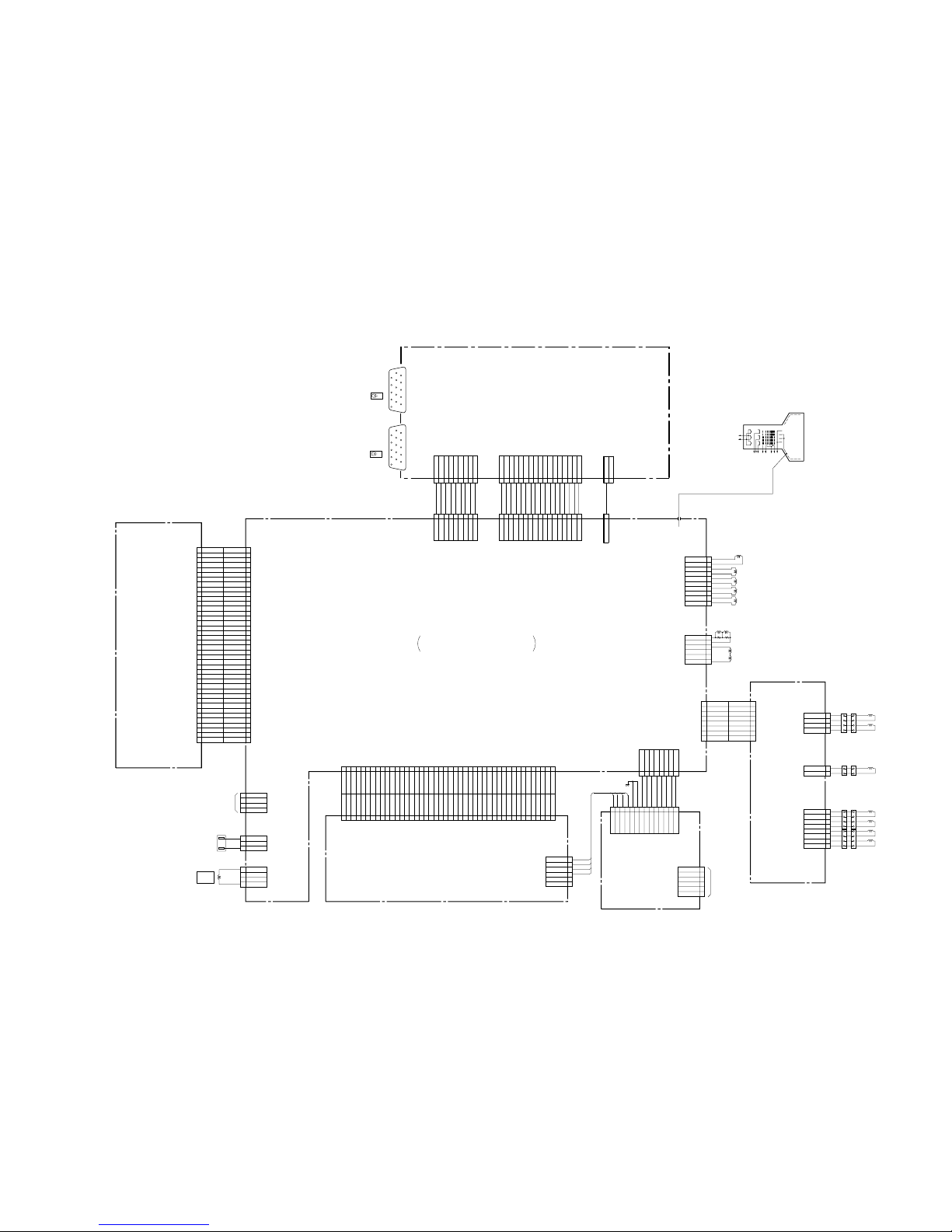
4-2. FRAME SCHEMATIC DIAGRAM
AC IN
LCC-NS
D
HV
DEFLECTION,HDF,VDF,
HV, POWER SUPPLY
B-SS3602<AEP>-KESSENZU-EPS05
H
G1
G2
HG
RGB
PICTURE
TUBE
1.2kV
CN504
1P
1
5
4
3
2
1
10
9
8
7
6
15
14
13
12
11
5
4
3
2
1
10
9
8
7
6
15
14
13
12
11
1
2
CN318
2P
G2
G2(NC)
CN1001
44P
4443424140393837363534333231302928272625242322212019181716151413121110
987654321
NC
GNDNCNC
POC
PLL LOCK
GNDS7WAKE UP
KEY SCAN
IK SIGMA
LED1
LB DET
LED2
V.FBP
INPUT SWS0+5VS1DGC SWS2PWR SW
GND
HTR SW
GND
GNDS3DDC GND2S4DDC SCL2S5DDC SDA2S6DDC GND1G2DDC SCL1
ABL DET
DDC SDA1
HV DET
ECO SW
RXD
IIC SCL
TXD
IIC SDA
CN1104
44P
4443424140393837363534333231302928272625242322212019181716151413121110
987654321
NC
GND
NC
NC
POC
PLL LOCK
GND
S7
WAKE UP
KEY SCAN
IK SIGMA
LED1
LB DET
LED2
V.FBP
INPUT SW
S0
+5V
S1
DGC SW
S2
PWR SW
GND
HTR SW
GND
GND
S3
DDC GND2
S4
DDC SCL2
S5
DDC SDA2
S6
DDC GND1
G2
DDC SCL1
ABL DET
DDC SDA1
HV DET
ECO SW
RXD
IIC SCL
TXD
IIC SDA
CN311
17P
WHT
17161514131211
10
987654321
GND
IIC SDA
IIC SCA
GND
ECO SW
GND
DDC SDA1
DDC SCL1
DDC GND1
DDC SDA2
DDC SCL2
DDC GND2
GND
INPUT SW
VS OUT
HS OUT
H BLK
CN312
9P
WHT
987654321
5V
3.3V7V+12V
GND
+80VNC+B
+B
CN604
9P
BLK
987654321
5V
3.3V
7V
+12V
GND
+80V
NC
+B
+B
CN1102
17P
BLK
17161514131211
10
987654321
GND
IIC SDA
IIC SCA
GND
ECO SW
GND
DDC SDA1
DDC SCL1
DDC GND1
DDC SDA2
DDC SCL2
DDC GND2
GND
INPUT SW
VS OUT
HS OUT
H BLK
N
(
µ-COM
)
H1
(
USER CONTROL
)
L2
(
CY, LCC
)
DA
(
DPU
)
A1
(VIDEO AMP, RGB OUT )
CN1101
40P
40
39
38
37
36
35
34
33
32
31
30
29
28
27
26
25
24
23
22
21
20
19
18
17
16
15
14
13
12
11
10
9
8
7
6
5
4
3
2
1
CN502
40P
40
39
38
37
36
35
34
33
32
31
30
29
28
27
26
25
24
23
22
21
20
19
18
17
16
15
14
13
12
11
10
9
8
7
6
5
4
3
2
1
XSC
YSC
D.TILT
XDC
HFBP
YDC
HD OUT
REFDC
HSHAPE
+12V
NC
+12V
A.GND
3.3V
D.GND
D.GND
HSAW_SW
GXSC
LCC NS
GYSC
IIC SDA
IIC SCL
A.GND
A.GND
H.LINBAL
H BLK
NC
HS OUT
DCC2
VS OUT
VSAWN
NC
A.GND
PLL LOCK
A.GND
POC
A.GND
A.GND
V.DF
H.DF
XSC
YSC
D.TILT
XDC
HFBP
YDC
HD OUT
REFDC
HSHAPE
+12V
NC
+12V
A.GND
3.3V
D.GND
D.GND
HSAW_SW
GXSC
LCC NS
GYSC
IIC SDA
IIC SCL
A.GND
A.GND
H.LINBAL
H BLK
NC
HS OUT
DCC2
VS OUT
VSAWN
NC
A.GND
PLL LOCK
A.GND
POC
A.GND
A.GND
V.DF
H.DF
CN1103
8P
WHT
8765432
1
INPUT SW
+5V
GND
LED 2
LED 1
KEY SCAN
WAKE UP
+12V
CN1400
14P
CN1003
6P
:S-MICRO (L)
1413121110
987654321
VX
VY
T_AMB
GND
GND
GND
INPUT SW
+5V
GND
LED 2
LED 1
KEY SCAN
WAKE UP
+12V
1
2
3
4
5
6
GND
VX
VY
T_AMB
LUMI (NC)
5V (NC)
CN1401
5P
TO
MAGNETIC
SENSOR
1
2
3
4
5
6
GND
VX
VY
T_AMB
LUMI (NC)
5V (NC)
CN1101
40P
1
2
3
4
5
6
7
8
CN1603
8P
WHT
1
2
3
4
5
6
7
8
-15V
+15V
GND
GXSC
GYSC
LCC_NS
IIC SDA
IIC SCL
-15V
+15V
GND
GXSC
GYSC
LCC_NS
IIC SDA
IIC SCL
10
9
8
7
6
5
4
3
2
1
ROTATION+
ROTATION–
XSC–
XSC+
YSC–
YSC+
XDC–
XDC+
YDC–
YDC+
CN701
10P
WHT
:S-MICRO
ROTATION
12LCC-NS (+)
LCC-NS (–)
CN1600
2P
WHT
:S-MICRO
1
2
3
4
5
6
7
8
LCC-LT (+)
LCC-LT (–)
LCC-LB (+)
LCC-LB (–)
LCC-RT (+)
LCC-RT (–)
LCC-RB (+)
LCC-RB (–)
CN1602
LCC-LT
LCC-LB
LCC-RT
LCC-RB
3
4
1
2
CY4+
CY4–
CY3+
CY3–
CN1601
4P
WHT
:S-MICRO
V DY
H DY
CN501
6P
WHT
:VH
1
2
3
4
5
6
V+
V–
NC
H–
NC
H+
DGC
1
2
3
4
DGC
NC
NC
DGC
CN601
4P
WHT
:VH
CN602
3P
WHT
:VH
1
2
3
AC L
NC
AC N
1
2
3
4
D GND
+5V
RXD
TXD
CN1101
4P
WHT
TO ECS
CN309
HD15D-SUB
CN307
HD15D-SUB
2
1
 Loading...