

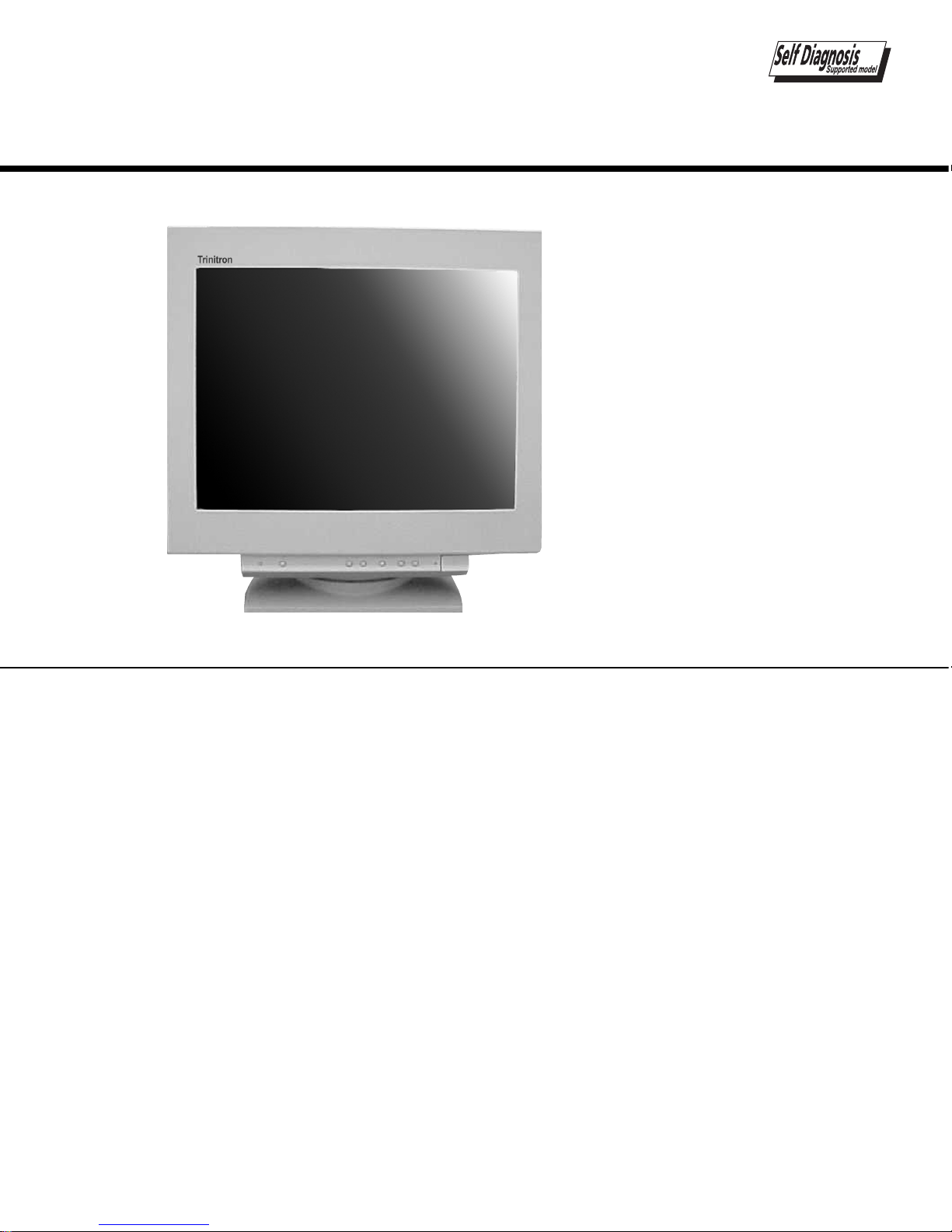
Sony TRINITRON CDP-4402 Service Manual
SPECIFICATIONS
F99
Picture tube
Video image area
Resolution
Standard image
area
Input signal
Video
Sync
0.24 mm (center) -0.25mm (edge)
aperture grill pitch
19 inches measured diagonally
90-degree deflection
(18" maximum viewing image)
Approx. 364.8 X 273.6 mm (w/h)
(14
3/8
x 10
7/8
inches)
Horizontal: Max. 1600 dots
Vertical: Max. 1200 lines
Approx. 352 x 264 mm (w/h)
(13
7/8
x 10
1/2
inches)
Analog RGB (75 ohms typical)
0.7 Vp-p, Positive
Separate Horizontal and Vertical
TTL level, Positive or Negative
Video Composite (Sync on Green)
0.3 Vp-p
Power Consumption
Maximum
Nominal
Deflection frequency
AC input voltage/current
Dimensions
Mass
CHASSIS
140 W, 478 BTU/h
100 W, 341BTU/h
Horizontal: 30 to 107 KHz (automatic)
Vertical: 48 to120 Hz (automatic)
220 to 240V, 50/60Hz,
1.0A (RMS) at 240 VAC
449 x 463 x 463 mm (w/h/d)
(17
2/3
x 18
7/10
x 18
1/5
inches)
Approx. 26.0 kg (57 lb 5 oz)
SERVICE MANUAL
Design and specifications are subject to change without notice.
CPD-4402
TRINITRON® COLOR MONITOR
CPD-4402
AEP Model
Chassis No. SCC-L30N-A
CPD-4402
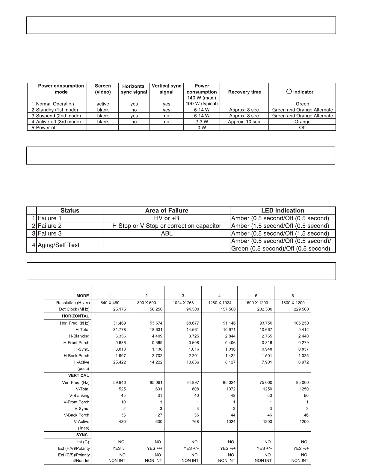
If you have VESA's DPMS compliance display card or software installed in your PC, the monitor can automatically reduce
its power consumption when not in use. If input from keyboard, mouse, or other input devices is detected, the monitor
will automatically "wake up." The following table shows the power consumption and signaling of this automatic power
saving feature.
When a failure occurs, the STANDBY/TIMER lamp will flash a set number of times to indicate the possible cause of the
problem. If there is more than one error, the lamp will identify the first of the problem areas.
SELF DIAGNOSTIC FUNCTION
POWER MANAGEMENT MODES
TIMING SPECIFICA TIONS

TABLE OF CONTENTS
Section Title Page
SAFETY CHECK-OUT .......................................................................................................................... 4
1. DISASSEMBL Y
1-1. Cabinet/Shield Removal ............................................................................................ 5
1-2. Service Position .......................................................................................................... 5
1-3. D, A, H and N Board Removal .................................................................................... 5
1-4. Picture Tube Removal................................................................................................ 6
2. SAFETY RELA TED ADJUSTMENTS
2-1. HV Regulator Check................................................................................................... 7
2-2. HV Protector Check .................................................................................................... 7
2-3. Beam Current Protector Check (Software Logic)...................................................... 7
2-4. B± Maximum Check.................................................................................................... 7
3. ADJUSTMENTS
3-1. Landing Rough Adjustment ....................................................................................... 8
3-2. Landing Fine Adjustment ........................................................................................... 8
3-3. Convergence Rough Adjustment ............................................................................... 8
3-4. Convergence Fine Adjustment ................................................................................... 8
3-5. Zero Positions of Ring Magnets ................................................................................ 9
3-6. White Balance Adjustment Specification ................................................................... 9
3-7. Vertical and Horizontal Position and Size Specification............................................ 9
3-8. Convergence Specification......................................................................................... 9
3-9. Focus Adjustment ....................................................................................................... 9
4. DIAGRAMS
4-1. Block Diagram .......................................................................................................... 10
4-2. Circuit Boards Location ............................................................................................ 12
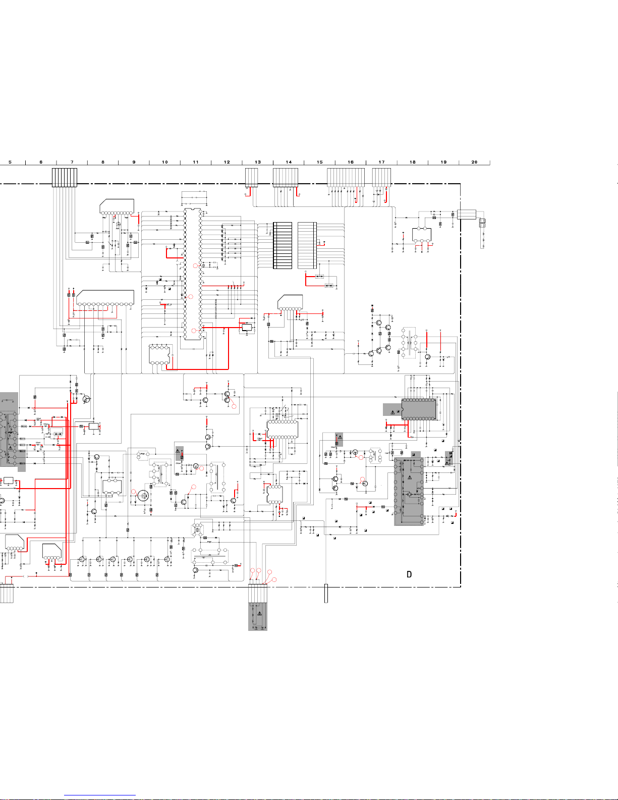
4-3. Schematic Diagrams and Printed Wiring Boards ................................................... 1 2
• D Board - Schematic Diagram ............................................................................. 1 3
• A Board - Schematic Diagram .............................................................................. 19
• H Board - Schematic Diagram ............................................................................. 2 1
• N Board - Schematic Diagram ............................................................................. 2 2
4-4. Semiconductors ....................................................................................................... 24
5. EXPLODED VIEWS
5-1. Chassis .................................................................................................................... 26
5-2. Packaging Materials ................................................................................................. 27
6. ELECTRICAL PARTS LIST ......................................................................................................... 28

SAFETY CHECK-OUT
After correcting the original service problem, perform
the following safety checks before releasing the set to
the customer:
1. Check the area of your repair for unsoldered or poorlysoldered connections. Check the entire board surface
for solder splashes and bridges.
2. Check the interboard wiring to ensure that no wires
are “pinched” or contact high-wattage resistors.
3. Check that all control knobs, shields, covers, ground
straps, and mounting hardware have been replaced.
Be absolutely certain that you have replaced all the
insulators.
4. Look for unauthorized replacement parts, particularly
transistors, that were installed during a previous
repair. Point them out to the customer and
recommend their replacement.
5. Look for parts which, though functioning, show
obvious signs of deterioration. Point them out to the
customer and recommend their replacement.
6. Check the line cords for cracks and abrasion.
Recommend the replacement of any such line cord
to the customer.
7. Check the B+ and HV to see if they are specified
values. Make sure your instruments are accurate; be
suspicious of your HV meter if sets always have low
HV.
8. Check the antenna terminals, metal trim, “metallized"
knobs, screws, and all other exposed metal parts for
AC Leakage. Check leakage as follows.
LEAKAGE TEST
The AC leakage from any exposed metal part to earth ground
and from all exposed metal parts to any exposed metal part
having a return to chassis, must not exceed 0.5 mA (500
microampere). Leakage current can be measured by any one
of three methods.
1. A commercial leakage tester, such as the Simpson 229
or RCA WT-540A. Follow the manufacturers' instructions
to use these instructions.
2. A battery-operated AC milliammeter. The Data Precision
245 digital multimeter is suitable for this job.
3. Measuring the voltage drop across a resistor by means of
a VOM or battery-operated AC voltmeter. The "limit"
indication is 0.75 V, so analog meters must have an
accurate low voltage scale. The Simpson's 250 and Sanwa
SH-63TRD are examples of passive VOMs that are
suitable. Nearly all battery operated digital multimeters
that have a 2V AC range are suitable. (See Figure A)
To Exposed Metal
Parts on Set
AC
0.15 µF
1.5 k
Ω
Earth Ground
Voltmeter
(0.75 V)
WARNING!!
NEVER TURN ON THE POWER IN A CONDITION IN WHICH THE
DEGAUSS COIL HAS BEEN REMOVED.
SAFETY-RELA TED COMPONENT W ARNING!!
COMPONENTS IDENTIFIED BY SHADING AND MARK ON THE
SCHEMA TIC DIAGRAMS, EXPLODED VIEWS AND IN THE P ARTS
LIST ARE CRITICAL FOR SAFE OPERATION. REPLACE THESE
COMPONENTS WITH SONY PARTS WHOSE PART NUMBERS
APPEAR AS SHOWN IN THIS MANUAL OR IN SUPPLEMENTS
PUBLISHED BY SONY. CIRCUIT ADJUSTMENTS THAT ARE
CRITICAL FOR SAFE OPERATION ARE IDENTIFIED IN THIS
MANUAL. FOLLOW THESE PROCEDURES WHENEVER CRITICAL
COMPONENTS ARE REPLACED OR IMPROPER OPERATION IS
SUSPECTED.
Figure A
AVERTISSEMENT!!
NE JAMAIS METTRE SOUS TENSION QUAND LA BOBINE DE
DEMAGNETISATION EST ENLEVEE.
ATTENTION AUX COMPOSANTS RELA TIFS A LA SECURITE!!
LES COMPOSANTS IDENTIFIES P AR UNE TRAME ET P AR UNE
MARQUE SUR LES SCHEMAS DE PRINCIPE, LES VUES
EXPLOSEES ET LES LISTES DE PIECES SONT D'UNE
IMPORTANCE CRITIQUE POUR LA SECURITE DU
FONCTIONNEMENT. NE LES REMPLACER QUE PAR DES
COMPOSANTS SONY DONT LE NUMERO DE PIECE EST
INDIQUE DANS LE PRESENT MANUEL OU DANS DES
SUPPLEMENTS PUBLIES PAR SONY. LES REGLAGES DE
CIRCUIT DONT L'IMPORTANCE EST CRITIQUE POUR LA
SECURITE DU FONCTIONNEMENT SONT IDENTIFIES DANS
LE PRESENT MANUEL. SUIVRE CES PROCEDURES LORS DE
CHAQUE REMPLACEMENT DE COMPOSANTS CRITIQUES, OU
LORSQU'UN MAUVAIS FONTIONNEMENT SUSPECTE.

CPD-4402
1
2
A board
D board
rotate 180º
1-3. D, A, H and N BOARD REMOVAL
1-1. CABINET/SHIELD REMOV AL 1-2. SERVICE POSITION
SECTION 1
DISASSEMBLY
1 When the D board is placed in service position, the Safety Earth Wire
(black wire) is disconnected.
2 After service is completed and the D board reinstalled, the Safety Earth
Wire must be reattached to the chassis. This must be confirmed before
any subsequent procedures are attempted.
To remove the rear cover of the unit, press in and unsnap the claw on
the right side of the unit, then press in and unsnap the right claw at the
top of the unit. Repeat this with the claw on the left side and top left
of the unit and remove.
Video shield
Two claws
Three screws
(+BVTT 4 x 8)
Two screws
(+ BVTP 4 x 16)
1
2
6
7
5
4
3
2
Two claws
Four screws
(+ BVTP 4 x 8)
Top cover
Bezel assembly
Bezel assembly
Cabinet
Cabinet
Push in the tip of a screwdriver
about 5mm to unlock the claw.
Cabinet
Three screws
(+BVTT 4 x 8)
8
Three screws
(+BVTT 4 x 8)
8
9
Side cover
9
Side cover
Cable bracket
D board
Five screws
(BVTP 3 x 8)
2
6
4
8
Holder
5
A board
N board
10
H board
11
One screw
(BVTT 4 x 8)
3
Three screws
(BVTT 4 x 8)
1
Two screws
(BVTT 4 x 8)
9
One screw
(BVTT 4 x 8)
7
One screw
(BVTT 4 x 8)
7
CPD-4402
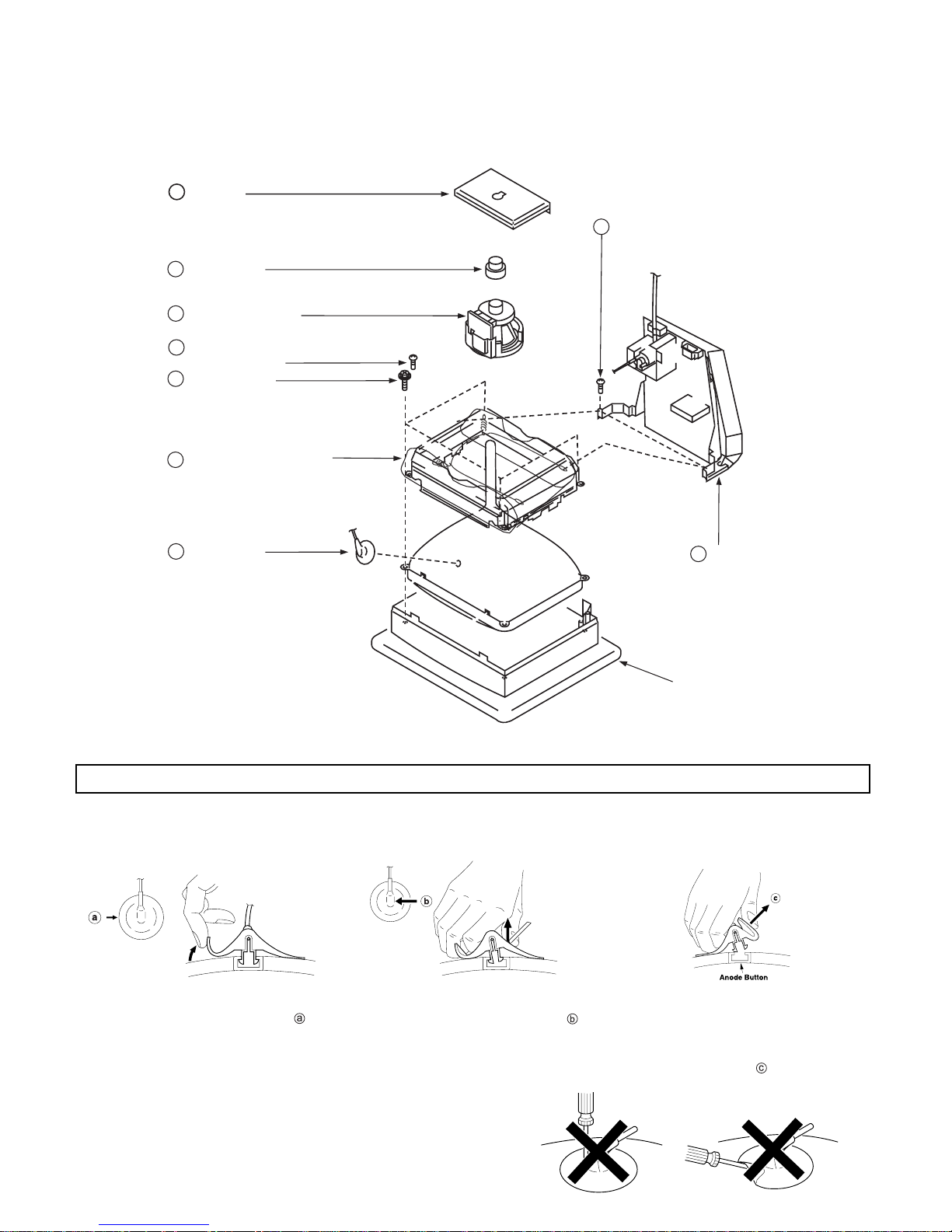
1-4. PICTURE TUBE REMOVAL
HOW TO HANDLE AN ANODE-CAP
1. Do not use sharp objects which may cause damage to the surface
of the anode-cap.
2. Do not squeeze the rubber covering too hard to avoid damaging the
anode-cap. A material fitting called a shatter-hook terminal is built into
the rubber.
3. Do not force turn the foot of the rubber cover. This may cause the
shatter-hook terminal to protrude and damage the rubber.
REMOVAL OF THE ANODE-CAP
WARNING: Short circuit the anode of the picture tube and the anode-cap to the metal chassis, CRT shield or carbon painted on the
CRT, after removing the anode.
REMOVAL PROCEDURES
A board
2
Neck ass'y
3
Deflection yoke
4
Four screws
(Tapping screw 5)
6
Anode-cap
1
Stand
ass'y
(D board)
8
Two screws
(BVTP 4 x 16)
7
Cushion
Tension spring
Demagnetization coil
Picture tube shield
9
Two screws
(BVTP 4 x 16)
5
2. Use your thumb to pull the rubber cap firmly
in the direction indicated by arrow .
1. Turn up one side of the rubber cap in
the direction indicated by arrow .
3. When one side of the rubber cap
separates from the anode button, the
anode-cap can be removed by turning
the rubber cap and pulling it in the
direction of arrow .

SECTION 2
SAFETY RELA TED ADJUSTMENT
When replacing parts shown in the table below, the following
operational checks must be performed as a safety precaution
against X-ray emissions from the unit.
Part Replaced ( )
HV ADJ
HV Protector T901 (FBT), R917, R918, R923, R920,
Circuit R919, R1004, C920, D91 1, D912
Beam Current R933, R932, R921, R1006, D915,
Protector Circuit D917, IC901, T901 (FBT)
HV Regulator T901 (FBT), IC901, R924, R925,
Circuit RV901
Allow the unit to warm-up for one minute prior to checking
the following conditions:
RV901
Part Replaced ( )
2-1. HV Regulator Check
1) Input white cross hatch signal. (fH = 106.3 kHz)
2) CONT and BRT Control normal condition.
3) Input voltage: 120 ± 2 VAC
4) Confirm that the voltage is within the voltage range shown
below .
Standard voltage: 27.0KV ± 0.2KV
5) When replacing components identified by
sure to recheck the High Voltage.
6) Verify the High V oltage as shown above (27.0KV
+0.2KV) is within specification. If not, RV904 on D board.
7) After adjusting the High Voltage within specification, put
the RV cover on RV901 as shown below and apply
sufficient amount of RTV around RV901.
, make
2-2. HV Protector Check
1) Confirm the voltage more than 15.0 VDC between D912
cathode and GND on D Board.
2) Using an external DC power supply, apply the voltage
shown below between cathode of D915 on D Board and
GND.
Confirm that the HV protector circuit (Hold down) works
and CRT screen disappears when applying the voltage
protector as shown below.
Standard DC Voltage: 21.1 +0.00 / - 0.05 VDC
Check Condition
• Input voltage : 120 ± 2 VAC
• Input signal : (fH = 31.4 kHz), Cross Hatch
• CONT and BRT Control: Normal Condition
2-3. Beam Current Protector Check
(Software Logic)
1) Using an external current source, apply 1.68mA from pin
of T901 (FBT) to GND on D Board. Confirm that the
software logic beam current protector works and that the
CRT screen disappears.
Check Condition
• Input voltage : 120 ± 2 VAC
• Input signal : (fH = 31.4 kHz), Cross Hatch
• CONT and BRT Control: Normal Condition
2-4. B± Maximum Check
1) Input white cross hatch (fH = 106.3 kHz) signal.
2) Beam control: Normal condition
3) Input voltage: 100 - 120 VAC
Note: Use NF power supply or make sure that
distortion factor is 3% or less.
4) Confirm that the voltage is within the voltage range
shown below.
Standard voltage: 195.0 -205.0 VDC
RV901
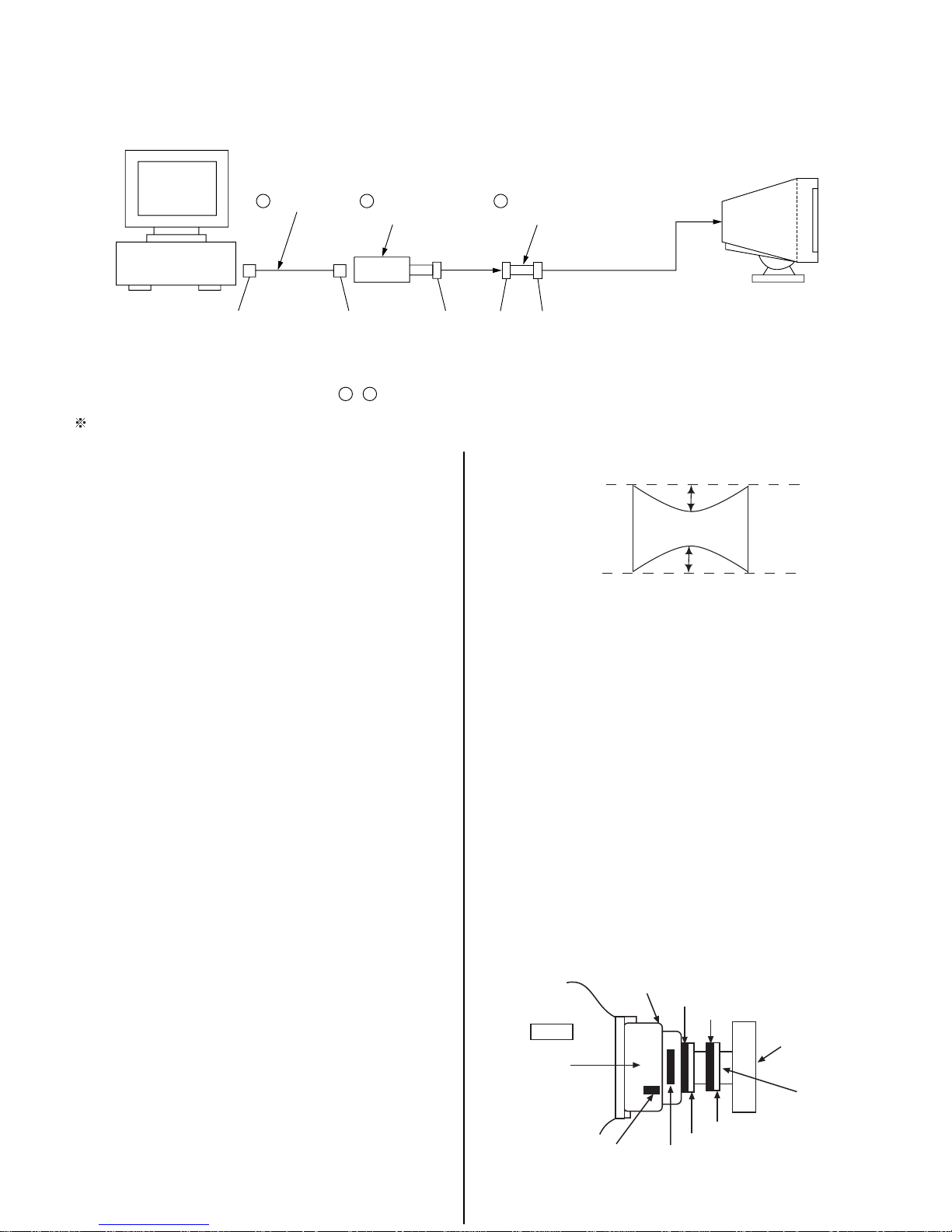
SECTION 3
a
b
ADJUSTMENTS
Connect the communication cable of the connector located on the D board on the monitor. Run the service software and then follow
these instructions.
IBM AT Computer
as a Jig
1-690-391-21
1
D-sub
(9 Pin [female])
*The parts above ( ~ ) are necessary for DAS adjustment.
mini Din
(8Pin)
1
A-1500-819-A
2
Interface Unit
3
4 Pin
3
4 Pin 4 Pin
Allow a 30 minute warm-up period prior to making the following adjustments:
3-1. Landing Rough Adjustment
1. Enter the full white signal.
2. Adjust the contrast to the maximum.
3. Input full green signal.
(Note: Turn off the outputs from R ch and B ch of SG)
4. Move the DY backward and adjust the purity magnet
coarsely so that a green raster positions in the center of
screen.
5. Moving the DY forward, adjust so that an entire screen
becomes pure green.
6. Adjust DY Tilt, use TLV of DY for this adjustment. Fix
the Register "TILT" to 0.
7. Lightly tighten the DY screw.
14. If landing does not meet specifications, correct with a
15. Perform auto-degauss.
16. Remove sensor and wobbling coil.
17. Confirm that there is no DY tilt. Affix purity magnet on
3-702-691-01
Connector Attachment
To BUS CONNECTOR
disc magnet.
DY using white paint.
3-2. Landing Fine Adjustment
1. Place the set in the Helmholtz coil.
2. Set TLH plate to the zero position.
3. Adjust Purity Magnet on the Neck Assembly to zero
position and secure it with white pin.
4. Set "VPIN SAW TOP" and "VPIN SAW BTM" to zero
position.
5. Display a plain green pattern.
6. Degauss CRT and shield with hand-degausser.
7. Perform auto-degauss.
8. Attach a wobbling coil to the specified position of CRT.
9. Attach a landing adjuster sensor on the CRT.
10. Using a landing checker, adjust the DY position, purity,
tilt of DY.
11. Tighten the DY screw.
Clamping torque: 22 ± 2 kg.cm (2.2 ± 0.2 N.m)
12. Perform auto-degauss.
13. Adjust top and bottom pin pitching DY by up and down
with two wedges so that (a) is equal to (b)(see the figure
at right). Also, leave the yaw of DY to the physical
center position with another two wedges.
Fasten wedges so that DY does not move.
3-3. Convergence Rough Adjustment
1. Enter the white crosshatch signal.
2. Roughly adjust the H. STAT and V. STAT with a
four-pole magnet.
3. Roughly adjust HMC and VMC with a six-pole magnet.
3-4. Convergence Fine Adjustment
1. Display crosshatch pattern with R and B.
2. Adjust H. STAT and V. STAT with 4-pole magnet.
(Do not adjust H.STAT and V.STAT with resistor.)
TLV VR (Unused)
CRT
DY
XCV Core
2 Pole
6 Pole Mg
A Board
Neck Assy
2 Pole (Unused)
4 Pole Mg
TLH Plate
CPD-4402
A
B
b
b
a
a
3. Display white crosshatch pattern.
4. Adjust HMC and VMC with 6-pole magnet.
5. Display crosshatch pattern with R and B.
6. Adjust H.STAT and V.STAT with 4-pole magnet.
7. Fine adjust H. STAT and V. STAT with use register
'HSTAT" and "VSTAT" in the range of 0 ± 10.
8. Adjust H.TILT with TLH plate.
or
Move of THL Plate
9. Adjust XCV with XCV core.
or
Move of XCV Volume
3-7. Vertical and Horizontal Position and
Size Specification
fH < 60 KHz
2.4 mm
2.4 mm
fH > 60 KHz
a
< 2.0 mm
b
< 2.4 mm
A B
264 352
3-8. Convergence Specification
C
A
Horizontal and Vertical
B
Prime Mode
A
< 0.25 mm
B
< 0.30 mm
C
< 0.35 mm
Other Mode
0.30 mm
0.35 mm
0.40 mm
10. Repeat steps 2-8 to optimize condition of whole screen.
11. Affix 4-pole magnet, 6-pole magnet and TLH plate and
XCV core with white paint.
3-5. Zero Positions of Ring Magnets
are Indicated by Arrows
[2pole magnet on DY] [4pole magnet]
[2pole magnet on Neck Assy][6pole magnet]
3-6. White Balance Adjustment
Specification
3-9. Focus Adjustment
Adjust focus (V) and focus (H) for optimum focus.
1. 9300K
x=0.283
y=0.298
2. 5000K
x=0.346
y=0.359
(All White)
(All White)
+0.015
+0.015
+0.015
+0.015
CPD-4402
— 10 —
1
2
3
4
5
6
1
2
43
5
6
1
2
3
4
5
6
7
8
1
2
3
4
5
6
7
8
9
1
0
1
1
1
2
1
3
1
4
1
5
1
2
3
4
5
6
7
8
9
1
0
1
1
1
2
1
3
1
4
1
5
1
2
3
4
5
6
7
8
1
2
3
11
G
R
D2001
X1001
IC607
CN2001
CN701
CN510
CN501
CN702
CN1005CN1006
PHOTOCOUPLER
CONTROL
3P
WHT
:S-MICRO
CY4-
CY3-
CY3+
CY2-
CY2+
CY1-
CY1+
CY4+
ROTATION-
ROTATION+
NC
1
237
6
5
G
N
D
H
F
B
P
H
S
H
A
P
E
H
D
O
U
T
N
C
C
B
L
A
N
K
+
5
V
-
2
G
N
D
H
S
Y
N
C
O
V
S
Y
N
C
O
P
O
C
P
L
L
L
O
C
K
I
I
C
D
A
T
A
I
I
C
C
L
K
D
S
P
R
E
S
E
T
O
OSCOUT
GND
GND
GND
KEY SCAN
LED1
LED2
GND
+5V
INPUT SEL
(FUNCTION CTRL)
IC1001
CPU
IC1003
RESET
IC1005
EPROM
H SIZE
ERROR
AMP
IC503
H CENTER
IC502
AMP
IC603
CONTROL
SW REG
IC605
REG
HEATER
12V
REG
IC608
ERROR
AMP
5V REG
IC609
STBY
IC702
D CONV OUT
IC701
S CONV OUT
IC901
DEFLECTION
CONTROL
IC501
ROTATION
IC703
V OUT
IC401
H DY+
H DY+
H DY-
H DY-
V DY-
V DY+
G
N
D
G
N
D
N
C
V
S
A
W
N
D
C
C
2
V
F
B
P
V
.
D
F
H
.
D
F
Y
D
C
R
E
F
D
C
X
D
C
D
.
T
I
L
T
X
S
C
Y
S
C
D
A
C
R
E
F
2
4
1
V FBP
V SAWN
DCC2
4
5
2
H.DF
6
3
7
T701
Q701
H DEF OUT
Q703,Q705
H DEF OUT
Q702,Q704
BUFFER
Q706
HV REG
Q901
HV OUT
Q902
H FBP
HD OUT
H
S
H
A
P
E
V DEF
T901
T902
HV
OUT
Q903,
Q904
1 KV
9
7
1
3
X
S
C
Y
S
C
IOUTA
INA-
INA+
INB+
INB-
IOUTB
4
6
DAC REF
REF DC
11
5
6
1
3
4
2
OUT B(Y)
OUT A(X)
-IN A(X)
STBY
-IN B(Y)
+IN A(X)
YDC
XDC
-IN B(Y)
FUNCTION
SWITCH
14
SW
Q501
11
3
5
PWMOUT
HVD
HDIN
Q502,
Q503
H
DRIVE
PWM OUT
6
7
9
18
11
10
14
3
REFIN
ERRIN
ERROUT
MIXOUT
MIX-
HDIN
VREG9
PWMOUT
S-CAPCHANGE
Q511-516
DRIVE
Q510
T503
T504
Q505
Q506
Q507
H OUT
T502
H SIZE
REG OUT
Q508,Q509
BUFFER
H RTRC
4
Q504
H DRIVE
T501
L503
Q519
Q517
2
1
4
2
3
45
44
SW
BUFFER
46 TO 50, 53
54
9
OUT
3
IN
5
6
SDA
SCL
7
WC
P6.7/SCLD
P6.6/SDAD
P3.7/HSYNCI2
P6.0/SDAI
P6.1/SCLI
VSYNCI2/INTO/P5.7
P5.0/HFBACK
WDOUT/INT2/P5.3
VSYNCO/P5.2
HSYNCO
AIN6/P6.3
WDIN/INT1/P5.5
INT3/P5.4
PWM6/P4.6
CLAMPOUT/MOIRE/P5.6
CSYNCI/P5.1
VSYNCI1
HSYNCI1
AIN3/P8.5
P8.6
P8.7
OSCIN
PWM3/P4.3
PWM5/P4.5
PWM4/P4.4
P9.1
RESET
36
37
34
35
33
27
25
32
21
1
22
20
30
28
15
51
52
26
18
23
24
7
8
5
16
17
39
38
SW
Q606
P3.6/SIN
P3.5/SOUT
PWM2/P4.2
INTCLK/P9.0
PWMN0/P4.0
AIN5/P6.4
AIN4/P6.5
T602
-15V
15V
80V
200V
12V
STBY
5V
PROT
Q609
1
3
Q605
SW REG
OUT
13
6
7
4
5
114
9
DEM
VAUX
DS
DRIVER
ISENSE
VCTRL
OOB
VIN
AC-RECT
D601
4
1
1
SW
Q607
BUFFER
BUFFER
Q2001
Q2002
(DEFLECTION)
(CONVERGENCE)
(POWER)
FBT
12V
200V
+STBY5V
5V-2
12V
SECTION 4
DIAGRAMS
G
A
F
CPD-4402
— 11 —
1
2
3
4
5
6
7
8
1
2
3
4
5
6
7
8
1
2
3
4
5
6
7
1
2
3
4
5
6
7
8
9
10
11
12
13
14
15
1
2
3
4
5
6
7
8
9
10
11
12
13
14
15
1
CN315
CN316
CN305
CN801
CN802
CN301
KB
GND
KG
GND
KR
GND
HEATER
GND
KB
GND
KG
GND
KR
GND
HEATER
GND
+12V
H1
GND
+80V
NC
GND
6
7
5
+200V
OUT
+
-
HSHAPE
HFBP
HD OUT
NC
CBLANK
D.GND
D.GND
+5V-2
PLL LOCK
POC
VSYNCO
HSYNCO
IICDATA
IICCLK
DSP RESET
V.DF
H.DF
A.GND
A.GND
VFBP
VSAWN
DCC2
NC
XDC
REFDC
YDC
YSC
DAC REF
XSC
D.TILT
TO D.BOARD
TO D.BOARD
CN1005
CN1006
(DSP)
48
47
46
44
40
42
64
58
H-OUT
FBP-IN
POC-OUT
BLK
H-IN
LOCK-DET
SDA
SCL
27
25
32
E/W
BUFFER
Q805
TILT
VDF1
HDF1
V-FBP
57
OUT
1
BUFFER
13
3
7
5
2
86
7
8
61
60
59
63
1
10
TEST19
VSAWN
39
DCC2
XDC
DCC
YDC
XSC
YSC
VDF2
Q804
BUFFER
Q801
PC1-FIL
V-IN
20
PC2-FIL
3.3V
5V
IN
OUT
OUT
+
OUT
+
IC801
DSP
IC803
V SAW
IC802
REG
BUFFER
Q002
BUFFER
Q003
1
3
4
5
6
7
8
17
16
15
14
Q006
Q001
X001
11
12
FBLK
ROUT
GOUT
BOUT
SDA
SCL
HFLY
VSYNC
HSYNC
XTALOUT
XTALIN
AV
BUFFER
G2 AMP
OSD
IC003
CONTROL
CUTOFF
IC005
27
23
20
11
9
8
5
3
1
B IN
G IN
B OUT
G OUT
R OUT
R.IN
G.IN
B.IN
G.OUT
B.OUT
R.OUT
R IN
10
11
12
32
31
30
15
16
14
13
6
5
4
3
29
1
SDA
SCL
CLAMP
BLK
B OSD
G OSD
R OSD
OSD BLK
G2
B BKG
G BKG
R BKG
V DET
15
14
13
3
5
7
R_OUT
G_OUT
B_OUT
R_IN
G_IN
B_IN
IC004
AMP
CUTOFF
RGBDRIVE
IC001
RGB OUT
IC002
KR
KG
KB
G2
7
8
9
J001
H
FC
FV
1 KV
1
(VIDEO)
10
F99-861-BD
5V-2
12V
4
13
12V
80V
200V
F
G
E
G
4-2. CIRCUIT BOARDS LOCATION
N
H
D
A
4-3. SCHEMATIC DIAGRAMS AND PRINTED WIRING BOARDS
Note:
• All capacitors are in µF unless otherwise noted. pF: µµF
50 WV or less are not indicated except for electrolytic.
• Indication of resistance, which does not have one for rating
electrical power, is as follows.
Pitch: 5 mm
Rating electrical power 1/4 W (CHIP: 1/10 W)
• All resistors are in ohms.
• : nonflammable resistor.
•
•
: fusible resistor.
: internal component.
• : panel designation and adjustment for repair.
• All variable and adjustable resistors have characteristic
curve B, unless otherwise noted.
: earth-ground
•
: earth-chassis.
•
• The components identified by in this basic schematic
diagram have been carefully factory-selected for each set in
order to satisfy regulations regarding X-ray radiation.
Should replacement be required, replace only with the value
originally used.
• When replacing components identified by
, make the
necessary adjustments by using RV901 ( ) as indicated.
(See page 7)
Note: The components identified by shading and
mark are critical for safety. Replace only with
part number specified.
Note: Les composants identifies per un trame et une
marque sont critiques pour la securite. Ne les
remplacer que par une piece portant le numero
specifie.
• When replacing parts shown in the table below, be sure to
perform the safety related adjustment.
HV ADJ
HV Regulator
Circuit
HV Protector
Circuit
Beam Current
Protector
Circuit
• All voltages are in volts.
• Readings are taken with a 10 M W digital multimeter
• Readings are taken with a color-bar signal input.
• V oltage variations may be noted due to normal production
tolerances.
• * : Cannot be measured.
• Circled numbers are waveform references.
•
•
: B +bus.
: B - bus.
Part Replaced ( )
RV901
Part Replaced ( )
D board T901, IC901, R924, R925,
RV901
D board T901, R917, R918, R923,
R920, R919, R1004, C920,
D911, D912
D board R933, R932, R921, R1006,
D915, D917, IC901, T901
— 13 —
CPD-4402
13
HV
17
14
15
16
11
12
FV1
FV2
4
1
2
6
8
10
9
7
5
1
2
3
4
5
6
7
8
9
1
0
1
1
1
2
1
3
1
4
1
5
1
6
1
7
1
8
1
9
2
0
2
1
2
2
2
3
2
4
2
5
2
6
2
7
282
9
3
0
3
1
3
2
3
3
3
4
3
5
3
6
3
7
3
8
3
9
4
0
4
1
4
2
4
3
4
4
4
5
4
6
4
7
4
8
4
9
5
0
5
1
5
2
5
3
5
4
5
5
5
6
S
1
3
4 5
6
8
2
4
5
6
10
1
9
1
1
2
3
4
1 2 3 4 5 6 7 8 9
10
1 2 3 4 5 6 7 8 9
10 11 12
1
2
3
4
5
6
7
8
9
10
11
12
13
14
15
1
2
3
4
5
6
7
8
9
10
11
12
13
14
15
1 2 3 4 5 6 7 8 9
10
11121314151617181920
1 2 3 4 5 6 7 8 9
101112131415161718
1234
5 6 7 8
IO
G
12345
2
3
5
7
8
9
10
11
12
13
14
15
16
17
18
1 2 3 4
5678
1
2
3
4
5
IO
G
-2 -2
-2
-2
-2
-2
-2
-2
-2
-2
-2
-2
-2
-2
-2
-2
-2
-2
-2
S
1
2
3
456
7
8
1 8
4 5
3
2
-2
1
2
3
4
5
6
-2
-2
1
2
3
4
5
6
7
8
9
1
0
1
1
1
2
-2
12345
-2
S
S
152
3
4
SS
12345
SSSS
1
2
3
4
5
6
7
8
1
2
3
4
5
6
12345
1
2
5
6
9
7
1
2
1 2 3 4 5 6 7
OUTVCC
GND
1
2
3
4
5
6
7
8
123
1
2
3
SG902
T502
R401
R403
R405
SG903
C930
R917
L901
C929
C409
L501
R407
R402
C402
L902
X1001
C1024
C1025
R1065
R1094
C1042
R1104
R1047
R1048
R1049
R1050
R1051
C1038
R1095
R1098
R1097
R1083
R901
SG901
RV901
C515
R503
R1096
R1073
R1074
R1085
L604
L603
L606
C1037
R735
R737
C1061
R418
R417
R416
R410
R409
L505
C503
C508
C510
R507
R509
R513
R516
R520
R524
R526
C518
C522
C523
R530
R532
R533
R535
R536
R537
R538
R540
C529
R544
R547
R550
R552
R553
R555
C539
C540
C541C543
C545
R557
R559
R561
R563
R564R565
R566
R567
R568
R902
C901
C902
C904
C905
C906
C909
C915 C916
R909 R910
R912
R915
C918
C919
C920
R916
R919
R920
R921
R923
C922
C923
C924
R924
R925
R926
R928
R929
R930
R931
C926
R701
R703
R705
R706
R707
R708
R709
R713
R714
R715
C704
C706
R717
C707
C708
R718
R719
R722
R725
C714
R731
R732
R733
R734
C716
R741
R744
R745
R746
C721
C724
R738
R753
R700
C609
R651
R657
C622
C623
C624
C629
C630
C631
C632
C633
R677
R679
R684
R685
R686
R687
R692
C650
R1086
C1026
C1006
C1036
R914
C712
R720
R721
R730
R729
R728
R727
R726
R724
R723 C711
C727
C726
C530
C531
C547
C701
C501
C703
C717
C718
C719
C723
C917
C921
C1013
C509
C512
R904
R905
C1031
R1070
R1072
C1050
C513
R579
R1011
R1015
R691
R573
R572
R569
R582
R1001
C553
C1030
C549
R747
R404
C516
R649
R650
R658
R748
R749
R751
C725
R523
R525
R528
R531
L504
C521
L506
L507
C653
C511
R504
R505
R740
C654
C551
C507
R515
C525
T701
R541
T504
R510
R508
C504
C514
C534
C535
R545
C559
R501 R502
R653
R664
C644
R652
C500
D1018
R406
R521
R697
R698
R576
C556
R570
C562
R752
C1062
L502
T503
L503
T602
C621
C1063
C1064
R1010
T901
R918
C908
R1005
R506
R1039
R584
C532
C903
R933
C564
C528
R549
C538
R932C563
C524
C557
C533
C608
C931
R1020
R1019
R1021
R
1
0
1
4
R1022
C1046
C1047
R527
R710
R711
R712
R659
C656
R681
R682
R680
R676
R755
R754
C555
R906
C925
R934
T902
R529
R539
R585
T501
R1013
R742
R743
R739
R518
R517
R577
R581
R583
R587
C658
C505
R736
R546
C537
R1017
R1018
C520
R927
C648
C628
C560
R574
R601
R908
C914
R911
C536
R548
L607
C646
C647
C401
C404
C403
R586
R519
R522
C558
C659
R408
C565
R542
R543
R512
R514
R511
R1007
C506
C900
R907
C1001
C1056
C1057
C406
C407
C527
C625
C626C627
C642
C657
C720
C728
C729
C730
C731
C907
C913
C927
FB501
R716
IC703
IC701
IC702
IC401
IC1003
IC1001
IC1005
IC901
IC501
IC604
IC609
IC502
IC503
IC605
Q706
Q705
Q703
Q701
Q704
Q702
FB901
Q901
Q903
Q904
Q902
Q509
Q508
Q501
Q503
Q502
Q606
Q609
Q519
Q517
D502
Q504
Q505
Q506
Q507
Q510
Q511Q512Q513
Q514
Q515
Q516
D1025
D1007
D1008
D1009
D1010
D1011
D1012
D1013
D1014
D1027
D1003
D1021
D1022
D1024
D620
D402
D401
D405
D622
D517
D519
D507
D508
D514
D509
D512
D518
D503 D510
D505
D511
D504
D501
D506
D515
D516
D615
D616
D614
D634 D635
D618
D617
D619D636
D623D613
D624
D630
D629
D701
D702
D703
D705
D901
D921
D920
D922
D916
D903
D904
D906
D907
D913
D909
D908
D910
D911
D914
D915
D912
C705
C732
R1008
R1092
R1004
R1006
R1084
R1046
R1012
R1016
JR603
JR604
JW1001
R645
R647
R648
FB1000
FB1001
FB1002
FB1004
C912
C911
D917
C910
FB502
R580
C554
C517
C713
C550
C548
C546
C544 C542
CN1003
CN1002
CN1001
CN701
CN1004
CN702
CN901
CN510
CN501
CN1005 CN1006
R575
0.01
:PT
1.5
:FPRD
1.5
1/2W
:RN
1.5
1/2W
:RN
2.2
:FPRD
22
100
22
:FPRD
330
1W
:RS
10p
CH:CHIP
10p
CH:CHIP
47p
CH:CHIP
0.01
B:CHIP
100k
0.01
B:CHIP
0.01
:PT
0.0022
100V
:PT
22k
1
:FPRD
27
1W
:RS
4.7k
3.3k
:RN-CP
0.1
25V
B:CHIP
22
0.01
B:CHIP
3.3k
:RN-CP
22k
:RN-CP
22k
:RN:CP
22k
:RN-CP
47k
:RN-CP
47k
:RN-CP
0.01
:PT
10
:FPRD
39
:RN
1M
47k
47k
47k
47k
47k
47k
100
25V
0.01
B:CHIP
0.1
B:CHIP
470p
CH:CHIP
100
25V
0.0033
:PT
220
3W
:RS
220
3W
:RS
22
:FPRD
2000p
1.2kV
:PP
2.2
:FPRD
4.7
10
100
25V
10k
:RN-CP
270k
:RN-CP
330k
1/2W
:RC
4.7k
1/2W
:RC
4.7k
1/2W
:RC
0.1
100V
:PT
2.2
2.2
100
1W
:RS
27
1W
:RS
2.2
1W
:RS
15
1W
:RS
100
1W
:RS
2.2
1W
:RS
0.1
:PT
0.1
:PT
0.47
:FPRD
1000
25V
1000
25V
82
1W
:RS
1
2W
:RS
82
1W
:RS
1
2W
:RS
1.0
1.5
:FPRD
150
1W
:RS
1.0
:MPS
470
:FPRD
4.7
:FPRD
4.7
:FPRD
47
100V
10
:FPRD
100k
220
25V
470
470
220
10V
82k
:RN
10k
:RN-CP
100p
CH:CHIP
0.01
2kV
F
0.01
2kV
F
0.1
25V
B:CHIP
22
1W
:RS
100k
:RN
0.1
25V
F:CHIP
0.1
25V
F:CHIP
0.1
25V
F:CHIP
330p
B:CHIP
330p
B:CHIP
68p
CH:CHIP
68p
CH:CHIP
0.1
25V
B:CHIP
0.1
25V
F:CHIP
0.1
25V
F:CHIP
33
100V
0.1
25V
F:CHIP
0.1
25V
F:CHIP
0.1
25V
F:CHIP
0.1
25V
F:CHIP
0.1
25V
F:CHIP
1000
10V
0.1
25V
F:CHIP
0.1
25V
F:CHIP
2.2k
:RN-CHIP
4.7k
:RN-CHIP
4.3k
:RN-CHIP
2.2k
:RN-CHIP
4.7k
:RN-CHIP
100p
2kV
SL
470p
B
0.1 25V B:CHIP
0.1 25V B:CHIP
0.1
25V
F:CHIP
4.7mH
15k
:RN-CP
3.3k
:RN-CP
47k
:RN-CP
100
:FPRD
100
:FPRD
100
:FPRD
100
:FPRD
100
:FPRD
100
:FPRD
15k
:RN-CP
15k
:RN-CP
4.7k
:RN-CP
2.2k
:RN-CHIP
47k
:RN-CP
0.22
100V
:PT
0.1
25V
F:CHIP
2.7k
:RN-CP
0.47
3W
:RS
0.22 F:CHIP
10k
10k :RN-CP
100k
1/2W
:RC
4.7k
:RN
100
16V
22k
:RN-CHIP
1.8k
:RN-CP
22k
:RN-CP
2.7k
:RN-CP
4.7mH
0.022
B:CHIP
4.7k
33k
:RN-CP
0.1
25V
F:CHIP
0.1
F:CHIP
220p
CH:CHIP
0.0047
:PT
0.0047
:PT
0.1
25V
F:CHIP
0.1
25V
F:CHIP
0.1 25V B:CHIP
100p
CH:CHIP
0.0047
B:CHIP
0.01 B:CHIP
220p
B:CHIP
0.0022
B:CHIP
100p
500V
:B
1000
25V
220
25V
470p
2kV
B
22
MA111-TX
4.7mH
15k
:RN
3.3k
:RN-CP
47
1W
:RS
1.8
10W
:RN
100
4.7k
:RN-CP
9.1k
:RN-CP
2.7k
:RN-CP
10k
3W
:RS
47k
2W
:RS
0.56
1W
:RS
47k
2W
:RS
47k
3W
:RS
47k 3W :RS
4.7
1W
:RS
0.1
25V
B:CHIP
0.1
B:CHIP
0.1
25V
B:CHIP
47
25V
100
100V
220
16V
:FBT
2.2
F:CHIP
1M
:RN
220
0.033
:PT
4.7
250V
0.1
B:CHIP
68
1/2W
:FPRD
56
3W
:RS
8.2k
:RN-CP
4.3k
:RN-CP
100
16V
470
16V
47
25V
100
4700p
1.8kV
:PP
0.022
B:CHIP
0.68
250V
:PP
0.33
250V
:PP
0.15
250V
:PP
0.033
400V
:PP
3.3
0.33
200V
:PP
22k
:RN-CP
0.1
B:CHIP
0.47
25V
F:CHIP
47p CH:CHIP
47p CH:CHIP
47k
:RN-CP
10k
:RN-CP
15k
:RN-CP
0.12 1/2W :RF
0.12
1/2W
:RF
4.7k
82k
:RN
2.7k
:RN-CP
75k
:RN
56k
:RN
5MH
:HOC
10k
:RN-CP
12k
:RN-CP
0.47
:MPS
0.01
:PT
100k
:RN-CP
0.47
:FPRD
27k
10k
:RN-CP
47p
500V
8.2k
:RN-CP
390
:RN-CP
0.018
B:CHIP
0.16
400V
:PP
47
3W
:RS
6.8k
1/2W
:RC
0.082
250V
:PP
330
25V
220
250V
47
25V
:HCC
470k
:CHIP
220k
:CHIP
100
:CHIP
220
:CHIP
22k
:CHIP
47k
:CHIP
220
:CHIP
220
:CHIP
120k
:CHIP
2.2k
:CHIP
2.2k
:CHIP
2.2k
:CHIP
100
:CHIP
22
:CHIP
39k
:CHIP
22k
:CHIP
22k
:CHIP
2.2k
:CHIP
8.2k
:CHIP
47k
:CHIP
5.6k
:CHIP
330
:CHIP
33k
:CHIP
100k
:CHIP
47k
:CHIP
2.2k
:CHIP
470
:CHIP
47k
:CHIP
220
:CHIP
47
:CHIP
1
0
0
:
C
H
I
P
220
:CHIP
2.2k
:CHIP
2.2k
:CHIP
47
:CHIP
47
:CHIP
100
:CHIP
100
:CHIP
100
:CHIP
100
:CHIP
470k
:CHIP
15k
:CHIP
15k
:CHIP
:HDT
:LCT
:SRT
:HRC
1
10V
B:CHIP
82
4.7k
470
25V
220
470
25V
100
16V
:HT
100
16V
:HT
150
1/2W
:FPRD
100k :CHIP
100
:CHIP
0.22
3W
:RS
4.7k
22
:FPRD
100
:CHIP
2.2k
:CHIP
680p
B:CHIP
:HST
1.0
B:CHIP
22k
:CHIP
220p
CH:CHIP
:DFT
0.047
250V
:MPS
0.47
400V
1.5
250V
:PP
0.0047
250V
E
0.047
250V
:MPS
0.047
250V
:MPS
120
:RN
120
:RN
120
:RN
150k
1/2W
0.47
:FPRD
:HLC
22
:FPRD
1k
:CHIP
1k
:CHIP
1k
:CHIP
1k
:CHIP
1k
:CHIP
1k
:CHIP
1k
:CHIP
1k
:CHIP
1k :CHIP
1k
:CHIP
1k :CHIP
1k :CHIP
2200
25V
:HT
22
250V
100
25V
10
10
10
100p
CH:CHIP
10k
:CHIP
10k
:CHIP
10k
:CHIP
10k
:CHIP
0
:CHIP
0
:CHIP
10k
:CHIP
10k
:CHIP
10k
:CHIP
10k
:CHIP
10k
:CHIP
10k
:CHIP
10k
:CHIP
10k :CHIP
4.7k
:CHIP
4.7k :CHIP
4.7k :CHIP
4.7k :CHIP
4.7k :CHIP
4.7k :CHIP
4.7k :CHIP
4.7k
:CHIP
4.7k :CHIP
4.7k :CHIP
4.7k
:CHIP
220p
220p
0.0022
:PT
0.0033
B:CHIP
0.0068
B:CHIP
0.001
25V
:HR
0.0018
25V
:HR
0.001
25V
:HR
0.0047
B:CHIP
0.001
500V
0.01
B:CHIP
0.0047
B:CHIP
0.0047
B:CHIP
0.0047
B:CHIP
0.0047
B:CHIP
0.001
CH:CHIP
33
250V
0.0022
200V
:PT
0UH
2.2
:FPRD
LA6500-FA
ROTATION
LA6510
S CONV OUT
STK391-110
D CONV OUT
LA78040
V OUT
PST574CMT-T1
RESET
CXD9523S/JCN
CPU
CAT2WC16J-TE13
EPROM
BA9758AFS-E2
PWR CONT
BA9759F-E2
DEFLECT CTRL
PQ12RD8S
12V REG
BA05T
STBY 5V REG
LA6500-FA
H CENTER AMP
NJM4558M-TE2
V DEF OUT
BA05ST-V5
HEATER REG
2SC3491A
V DEF
2SA1358
H DEF
2SA1049
H DEF
2SC2362KG
H DEF
2SC3421
BUFFER
2SC2459
BUFFER
0UH
IRFI9634G-LF35
HV REG
2SC2412K
HV OUT
2SA1036K
HV OUT
FS5KM-18A-AY
HV OUT
2SA1036K
BUFFER
2SC2411K
BUFFER
2SC1623
SW
2SA1037K
H DRIVE
2SC2411K
H DRIVE
DTC114EKA-T146
HEATER SW
2SC3311A
PROT
2SA1037AK
STBY SW
2SC3209LK
H CNT CTRL
D3S4M
IRFU110
H DRIVE OUT
2SC5445(LBSONY1)
H OUT
IRFI9634G-LF35
RE OUT
2SC2412K
H RTRC
2SC3311A
DRIVE
2SK2098
S CAP CHANGE
2SK2098
S CAP CHANGE
2SK2098
S CAP CHANGE
2SK2098
S CAP CHANGE
2SK2098
S CAP CHANGE
2SK2098
S CAP CHANGE
UDZ-TE-17-5.6B
UDZ-TE-17-5.6B
UDZ-TE-17-5.6B
UDZ-TE-17-5.6B
UDZ-TE-17-5.6B
UDZ-TE-17-5.6B
UDZ-TE-17-5.6B
UDZ-TE-17-5.6B
UDZ-TE-17-5.6B
4.7K :CHIP
680K :RN-CP
1PS226-115
1PS226-115
MA111-TX
D10SC9M
UDZ-TE-17-5.6B
EGP10GPKG23
1SS133T-77
D4L20U
UDZ-TE-17-15B
UTZ-4.7B
MA111-TX
MA111-TX
RD4.7ES-T1B2
MA111-TX
MA111-TX
RD10ES-T1B2
HZS182-TE MA111-TX
D2L40-TA
MA111-TX
PG124S15
HZS182-TE
UDZ4.7B
MA111-TX
ERA91-02TP1
UF4007G23
BT149G-412-OT359
FMC-26UA
1SS133T-77 1SS133T-77
ERB38-06V1
1SS133T-77
FMN-G12SUDZ-TE-17-12B
EGP10DPKG23RGP10DG23
EGP10DPKG23
MTZJ-T-77-15B
MA111-TX
1SS133T-77
1SS133T-77
1SS133T-77
UDZ-TE-17-12B
MA111-TX
UDZ-TE-17-5.6B
UDZ-TE-17-5.6B
MA111-TX
UDZ-TE-17-12B
MA111-TX
MA111-TX
UDZ-TE-17-15B
D2L40-TA
RD16ES-T1B2
UDZ-TE-17-15B
MA111-TX
RGP02-17PKG23
RGP02-17PKG23
HSS82
RD5.1ESBT1B2
RD16ES-T1B2
0.1
25V
B:CH
0.01
B:CH
1k
:CHIP
220
:CHIP
220 :CHIP
220
:CHIP
470
:CHIP
4.7k :CHIP
47
:CHIP
220
:CHIP
0
:CHIP
0
:CHIP
17.5MM
JW(7.5MM)
JW(7.5MM)
JW(7.5MM)
0
:CHIP
100
:CHIP
100
:CHIP
0
:CHIP
0.01
B:CH
47p
CH:CH
RD9.1ES-T1B2
220p
CH:CHIP
0UH
2.2k
:RN-CHIP
220p
CH:CHIP
330p
CH:CH
0.01
B:CHIP
0.01
B:CHIP 0.01
B:CHIP
0.01
B:CHIP
0.01
B:CHIP
0.01
B:CHIP
12P
WHT
S:MICRO
8P
WHT
:S-MICRO
4P
WHT
8P
WHT
:S-MICRO
6P
WHT
:S-MICRO
3P
WHT
:S-MICRO
TO CHASSIS
6P
15P 15P
2.2k
RN-CP
W
P
80V
12V
300V
300V
12V
12V
12V
12V
15V
-15V
15V
-15V
12V
-15V
12V
15V
-15V
15V
-15V
12V
15V
-15V
5V
5V-2
5V-2
80V
5V
5V
5V
5V
15V
-15V
5V-2
200V
200V
200V
200V
5V-2
5V
80V
12V-2
12V-2
12V-2
12V-2
5V
5V
12V-2
12V-2
S
0
S
1
S
2
S
3
S
4
S
5
L
E
D
1
L
E
D
2
X
D
C
Y
D
C
R
E
M
O
T
E
O
N
/
O
F
F
R
E
F
D
C
DCC2
V FBP
V.DF
H.DF
YDC
REF DC
XDC
V SAWN
D
.
T
I
L
T
R
O
T
A
T
I
O
N
Y
S
C
D
A
C
R
E
F
X
S
C
H.DF
H SHAPE
A
B
L
D
E
T
H
S
Y
N
C
C
P
U
G
N
D
1
R
X
D
T
X
D
C
B
L
A
N
K
I
N
P
U
T
S
E
L
B
P
C
L
A
M
P
C
S
Y
N
C
V
S
Y
N
C
H
S
Y
N
C
C BLANK
H SYNC0
V SYNC0
POC
PLL LOCK
DCC2
H
D
O
U
T
D
D
C
C
L
K
D
D
C
D
A
T
A
C
P
U
G
N
D
1
H
S
Y
N
C
0
V
S
Y
N
C
0
K
E
Y
S
C
A
N
C
P
U
G
N
D
2
H
E
A
T
E
R
HEATER
REMOTE ON/OFF
DEGAUSS
H.CENT
H.LIN BAL
R
E
M
O
T
E
O
N
/
O
F
F
H SYNC0
C SYNC
V SYNC0
POC
PLL LOCK
BP CLAMP
CPU GND2
KEY SCAN
HV DET
ABL DET
V SYNC
S0
LED2
LED1
S1
S2
S3
S4
S5
V FBP
TXD
RXD
DDC DATA
DDC CLK
V FBP
V SAWN
H FBP
H
F
B
P
H
.
L
I
N
B
A
L
H
V
D
E
T
D
E
G
A
U
S
S
ROTATION
D
A
C
R
E
F
V
.
D
F
V.DF2
V
.
D
F
2
H
F
B
P
H.CENT
XSC
DAC REF
YSC
HD OUT
H SHAPE
H FBP
D.TILT
IIC CLK
IIC DATA
IIC CLK
IIC DATA
I
I
C
D
A
T
A
I
I
C
C
L
K
I
I
C
D
A
T
A
I
I
C
C
L
K
INPUT SEL
I
N
P
U
T
S
E
L
C
Y
4
-
C
Y
3
-
C
Y
3
+
C
Y
2
-
C
Y
2
+
C
Y
1
-
C
Y
1
+
C
Y
4
+
ROTATION-
ROTATION+
H
D
Y
+
H
D
Y
+
H
D
Y
-
H
D
Y
-
V
D
Y
-
V
D
Y
+
D
G
N
D
R
X
D
T
X
D
1
.
0
K
V
I
O
U
T
A
O
U
T
A
I
N
A
-
I
N
A
+
V
E
E
I
N
B
+
I
N
B
-
O
U
T
B
I
O
U
T
B
V
C
C
L
E
D
1
L
E
D
2
G
N
D
+
5
V
O
U
T
B
(
Y
)
-
I
N
B
(
Y
)
+
I
N
B
(
Y
)
-
I
N
A
(
X
)
O
U
T
A
(
X
)
V
E
E
V
C
C
S
T
B
Y
+
I
N
A
(
X
)
PWM6/P4.6
PWM5/P4.5
VPP
TEST0
PWM4/P4.4
PWM3/P4.3
PWM2/P4.2
RESET
P3.0/TXCLK/CLKOUT
P8.7
PWM1/P4.1
PWMN0/P4.0
INTCLK/P9.0
P9.1
AVSS
P8.6
P8.1
P8.0
P3.1/TOUTA/CTS
P3.2/TOUT/DCD
AVVD
AIN0/P8.2
AIN1/P8.3
AIN2/P8.4
AIN3/P8.5
AIN4/P6.5
AIN5/P6.4
P3.3/BLANKOUT
OSCIN
OSCOUT
XT
P3.4/RXCLK
VSS
VDD
AIN6/P6.3
VSYNCI1
VSYNCI2/INTO/P5.7
CLAMPOUT/MOIRE/P5.6
WDIN/INT1/P5.5
INT3/P5.4
WDOUT/INT2/P5.3
VSYNCO/P5.2
HSYNCO
CSYNCI/P5.1
VSS
HSYNCI1
VDD
P5.0/HFBACK
P3.7/HSYNCI2
P6.7/SCLD
P6.6/SDAD
P6.1/SCLI
P6.0/SDAI
P3.6/SIN
P3.5/SOUT
HVD
AGC
+
-
PWMOUT
PVcc
N
C
S
A
W
O
U
T
N
C
S
G
N
D
H
D
I
N
D
E
L
A
Y
V
R
E
G
9
S
V
c
c
P
G
N
D
H
V
D
C
A
P
N
C
S
L
O
W
S
W
N
C
E
R
R
O
U
T
P
V
C
C
P
W
M
O
U
T
P
G
N
D
S
L
O
W
S
W
V
R
E
G
9
S
A
W
R
S
A
W
O
U
T
S
G
N
D
H
D
I
N
N
C
M
I
X
+
M
I
X
-
M
I
X
O
U
T
V
C
C
R
E
F
I
N
E
R
R
I
N
N
C
E
R
R
O
U
T
S
D
A
V
S
S
S
C
L
A
2
A
1
W
C
V
C
C
A
0
G
N
D
+
8
0
V
N
C
V
A
D
J
O
U
T
G
N
D
V
C
C
C
T
L
I
N
P
U
T
S
E
L
B
P
C
L
A
M
P
C
S
Y
N
C
V
S
Y
N
C
G
N
D
C
B
L
A
N
K
D
D
C
C
L
K
C
P
U
G
N
D
1
D
D
C
D
A
T
A
I
I
C
D
A
T
A
H
F
B
P
+
5
V
-
2
V
S
Y
N
C
0
H
S
Y
N
C
0
G
N
D
I
I
C
C
L
K
H
S
Y
N
C
S
T
B
Y
+
5
V
+
+
-
-
V
C
C
V
E
E
0
0
+
2
0
0
V
K
E
Y
S
C
A
N
C
P
U
G
N
D
2
STBY
STBY
STBY
STBY
STBY
STBY
NC
+
S
T
B
Y
5
V
STBY
AIN0/P6.2
STBY
I
N
P
U
T
S
W
G
N
D
F99-875-D
GND
GND
GND
H FBP
NC
H SHAPE
HD OUT
V SAWN
DCC2
V FBP
V.DF
H.DF
NC
YDC
REF DC
XDC
C BLANK
+5V-2
GND
H SYNCO
V SYNCO
POC
PLL LOCK
IIC DATA
IIC CLK
D.TILT
XSC
YSC
DAC REF
DSP RESET
(CONVERGENCE)
(DEFLECTION)
(POWER)
TO CONVERGENCE YOKE FOR SERVICE
TO A BOARD
CN309
TO A BOARD
CN306&310
TO H BOARD
CN2001
TO A BOARD
CN301
1
2
3
4
5
6
7
8
9
13
12
1110
 Loading...