

Sony Trinitoron CPD-G220 Service Manual
CHASSIS
SERVICE MANUAL
SPECIFICATIONS
CPD-G220
17VC
AEP Model
Chassis No. SCC-L38A-A
TORINITORON
®
COLOR GRAPHIC DISPLAY
CRT
0.24 mm aperture grille pitch(center)
17 inches measured diagonally
90-degree deflection
FD Trinitron
Viewable image size Approx. 327 × 243 mm (w/h)
×
(12 9 inches)
Resolution
Maximum Horizontal: 1600 dots
Vertical: 1200 lines
Recommended Horizontal: 1024 dots
Vertical: 768 lines
Standard image area
Deflection frequency*
AC input voltage/current 100 to 240 V, 50/60 Hz, Max. 1.7A
Power consumption Approx. 115 W
(without USB operation)
Dimensions
Approx. 402 ×
418 × 421mm (w/h/d)
(15
7
/8 × 16 1/2 ×16
Mass Approx. 19 kg (41.9 lb 1 oz)
Plug and Play DDC2B/DDC2Bi
GTF**
Supplied accessories
Power cord(1)
Macintosh G3/G4 adapter(1)
USB cable(1)
Warranty card(1)
Notes on cleaning the screen's surface(1)
Instruction manual(1)
*Recommended horizontal and vertical timing condition
•Horizontal sync width should be more than 1.0 µsec.
•Horizontal blanking width should be more than 3.0 µsec.
•Vertical blanking width should be more than 500 µsec.
**If the input signal is Generalized Timing Formula(GTF)
compliant, the GTF feature of the monitor will automatically
provide an optical image for the screen.
Design and specification are subject to change without notice.
Approx. 312 × 234 mm (w/h)
(12
3
/8 × 9 1/4inches)
Horizontal: 30 to 96 kHz
Vertical: 48 to 170 Hz
viewing image Approx. 408 mm (16.0 inches)
5
/
8
inches)
7
/
8
5
/
8
CPD-G220(E) 2
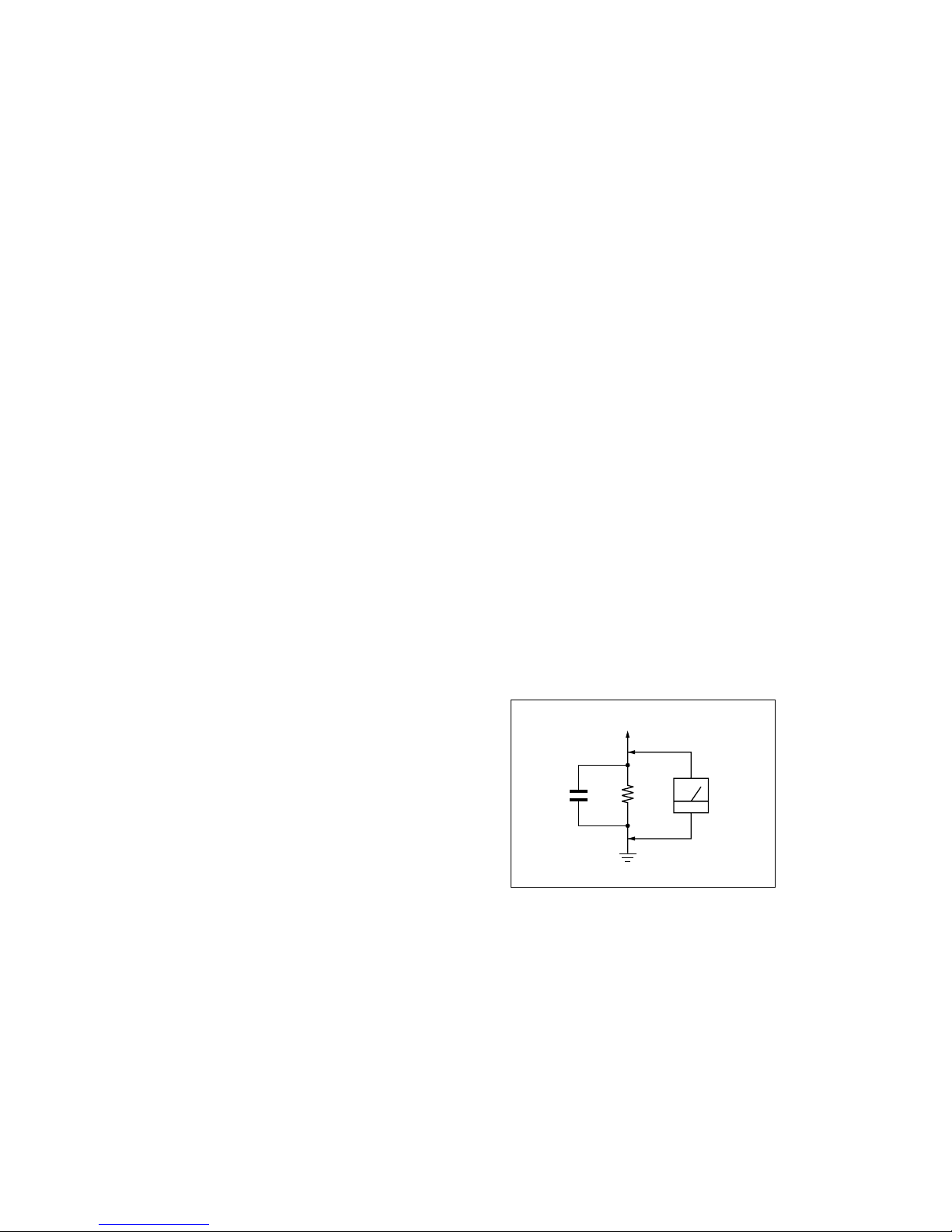
LEAKAGE TEST
The AC leakage from any exposed metal part to earth ground and from all
exposed metal parts to any exposed metal part having a return to chassis,
must not exceed 0.5 mA (500 microamperes).
Leakage current can be measured by any one of three methods.
1. A commercial leakage tester, such as the Simpson 229 or RCA WT540A. Follow the manufacturers’ instructions to use these instruments.
2. A battery-operated AC milliammeter. The Data Precision 245 digital
multimeter is suitable for this job.
3. Measuring the voltage drop across a resistor by means of a VOM or
battery-operated AC voltmeter. The “limit” indication is 0.75 V, so
analog meters must have an accurate low-voltage scale. The Simpson 250
and Sanwa SH-63Trd are examples of a passive VOMs that are suitable.
Nearly all battery operated digital multimeters that have a 2 V AC range
are suitable. (See Fig. A)
After correcting the original service problem, perform the following safety
checks before releasing the set to the customer:
1. Check the area of your repair for unsoldered or poorly-soldered
connections. Check the entire board surface for solder splashes and
bridges.
2. Check the interboard wiring to ensure that no wires are “pinched” or
contact high-wattage resistors.
3. Check that all control knobs, shields, covers, ground straps, and
mounting hardware have been replaced. Be absolutely certain that you
have replaced all the insulators.
4. Look for unauthorized replacement parts, particularly transistors, that
were installed during a previous repair. Point them out to the customer
and recommend their replacement.
5. Look for parts which, though functioning, show obvious signs of
deterioration. Point them out to the customer and recommend their
replacement.
6. Check the line cords for cracks and abrasion. Recommend the
replacement of any such line cord to the customer.
7. Check the B+ and HV to see if they are specified values. Make sure your
instruments are accurate; be suspicious of your HV meter if sets always
have low HV.
8. Check the antenna terminals, metal trim, “metallized” knobs, screws, and
all other exposed metal parts for AC Leakage. Check leakage as
described right.
Fig. A. Using an AC voltmeter to check AC leakage.
1.5 k
Ω
0.15 µF
AC
Voltmeter
(0.75 V)
To Exposed Metal
Parts on Set
Earth Ground
SAFETY CHECK-OUT

CPD-G220(E) 3
WARNING!!
NEVER TURN ON THE POWER IN A CONDITION IN WHICH THE
DEGAUSS COIL HAS BEEN REMOVED.
SAFETY-RELATED COMPONENT WARNING!!
COMPONENTS IDENTIFIED BY SHADING AND MARK ! ON THE
SCHEMATIC DIAGRAMS, EXPLODED VIEWS AND IN THE
PARTS LIST ARE CRITICAL FOR SAFE OPERATION. REPLACE
THESE COMPONENTS WITH SONY PARTS WHOSE PART
NUMBERS APPEAR AS SHOWN IN THIS MANUAL OR IN
SUPPLEMENTS PUBLISHED BY SONY. CIRCUIT ADJUSTMENTS THAT ARE CRITICAL FOR SAFE OPERATION ARE
IDENTIFIED IN THIS MANUAL. FOLLOW THESE PROCEDURES
WHENEVER CRITICAL COMPONENTS ARE REPLACED OR IMPROPER OPERATION IS SUSPECTED.
AVERTISSEMENT!!
NE JAMAIS METTRE SOUS TENSION QUAND LA BOBINE DE
DEMAGNETISATION EST ENLEVÉE.
ATTENTION AUX COMPOSANTS RELATIFS À LA SÉCURITÉ!!
LES COMPOSANTS IDENTIFIÉS PAR UNE TRAME ET UNE
MARQUE ! SONT CRITIQUES POUR LA SÉCURITÉ. NE LES
REMPLACER QUE PAR UNE PIÈCE PORTANT LE NUMÉRO
SPECIFIÉ. LES RÉGLAGES DE CIRCUIT DONT L’IMPORTANCE EST
CRITIQUE POUR LA SÉCURITÉ DU FONCTIONNEMENT SONT
IDENTIFIÉS DANS LE PRÉSENT MANUEL. SUIVRE CES
PROCÉDURES LORS DE CHAQUE REMPLACEMENT DE
COMPOSANTS CRITIQUES, OU LORSQU’UN MAUVAIS
FONCTIONNEMENT EST SUSPECTÉ.

CPD-G220(E) 4
POWER SAVING FUNCTION
This monitor meets the power-saving guidelines set by VESA, TCO’99,
and ENERGY STAR. If no signal is input to the monitor from your
computer, the monitor will automatically reduce power consumption as
shown below.
*
1
Figures reflect power consumption when no USB compatible
peripherals are connected to the monitor.
*2When your computer enters power saving mode, NO SIGNAL appears
on the screen. After a few seconds, the monitor enters power saving
mode.
*
3
“Deep sleep” is power saving mode defined by the Environmental
Protection Agency.
Power mode Power consumption*
1
f (power)
indicator
normal operation ≤ 115 W (without USB operation) green
active off*
2
(deep sleep)*
3
≤ 3 W orange
power off 0 W (approximately) off
CPD-G220(E) 5
DIAGNOSIS
Failre
Horizontal / Vertical Deflection failure,
(Included S-cap)
ABL protector
HV failure
Aging / Self Test
Out of scan range
Power LED
Amber → Off
(1.5 sec) (0.5 sec)
Amber → Off
(0.5 sec) (1.5 sec)
Amber → Off
(0.5 sec) (0.5 sec)
Amber → Off → Green → Off
(0.5 sec) (0.5 sec) (0.5 sec) (0.5 sec)
Green (OSD indication)
Aging Mode (Video Aging) : During Power Save, press MENU button for longer than 2 second.
Monitor Information and RGB bar : During Power Save, push CONT+ button for longer than 2 second.
ALL White : During Power Save, push CONT- button for longer than 2 second.
CPD-G220(E) 6
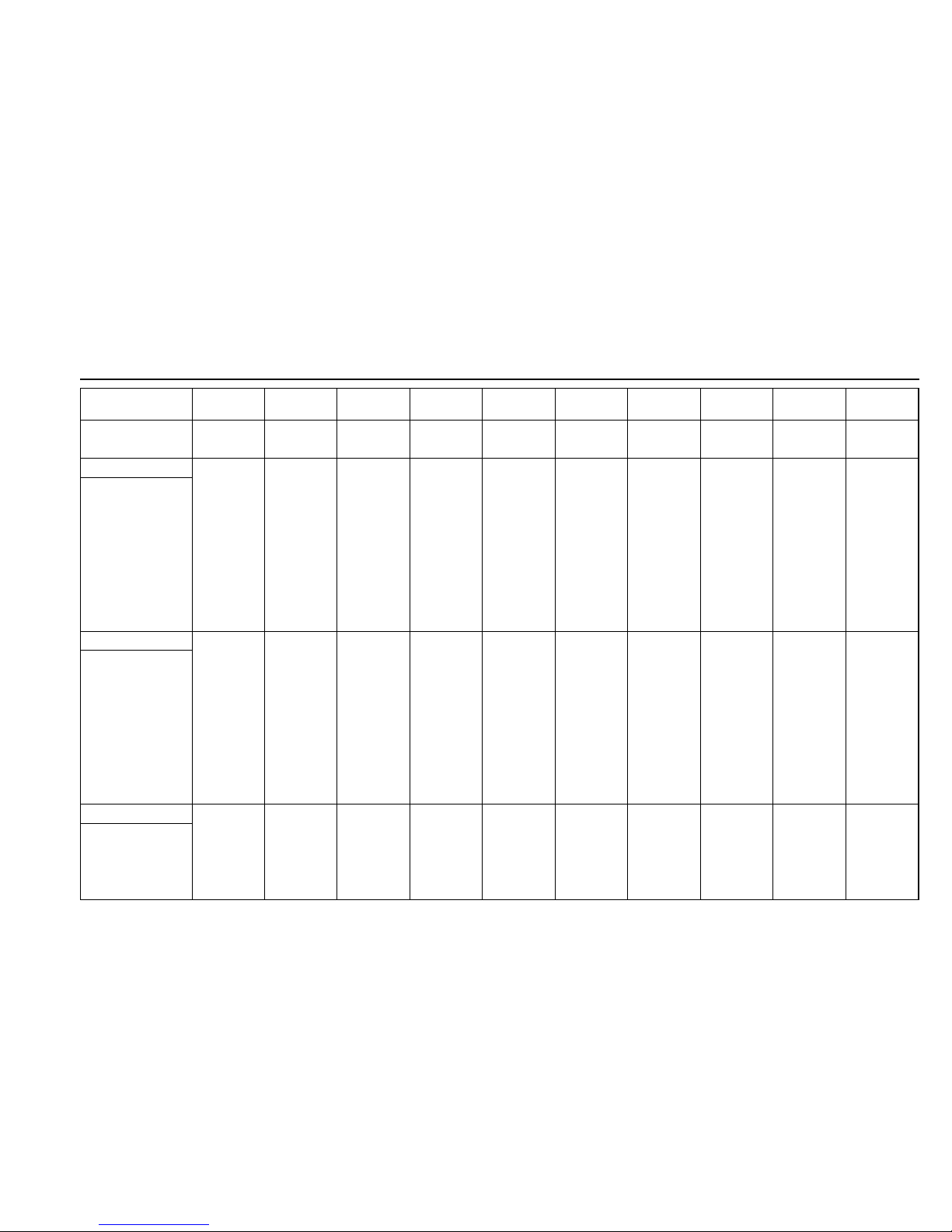
TIMING SPECIFICATION
MODE Primary Mode
MODE AT PRODUCTION
MODE 1 MODE 2 MODE 3 MODE 4 MODE 5 MODE 6 MODE 7 MODE 8 MODE 9 MODE 10
RESOLUTION
640 X 480 800 X 600 832 X 624 1024 X 768 1280 X 1024 1024 X 768 720 X 400 640 X 480 1280 X 1024 1600 X 1200
CLOCK
25.175 MHz 56.250 MHz 57.283 MHz 78.750 MHz 157.500 MHz 94.500 MHz 28.322 MHz 36.000 MHz 135.000 MHz 202.500 MHz
— HORIZONTAL —
H-FREQ
31.469 kHz 53.674 kHz 49.725 kHz 60.023 kHz 91.164 kHz 68.677 kHz 31.469 kHz 43.269 kHz 79.976 kHz 93.750 kHz
usec usec usec usec usec usec usec usec usec usec
H. TOTAL
31.778 18.631 20.111 16.660 10.971 14.561 31.777 23.111 12.504 10.667
H. BLK
6.356 4.409 5.586 3.657 2.844 3.725 6.355 5.333 3.022 2.765
H. FP 0.636 0.569 0.559 0.203 0.406 0.508 0.636 1.556 0.119 0.316
H. SYNC
3.813 1.138 1.117 1.219 1.016 1.016 3.813 1.556 1.067 0.948
H. BP
1.907 2.702 3.910 2.235 1.422 2.201 1.907 2.222 1.837 1.501
H. ACTIV
25.422 14.222 14.524 13.003 8.127 10.836 25.422 17.778 9.481 7.901
— VERTICAL —
V. FREQ (HZ)
59.940 Hz 95.061 Hz 74.550 Hz 75.029 Hz 85.024 Hz 84.997 Hz 70.087 Hz 85.008 Hz 75.025 Hz 75.000 Hz
lines lines lines lines lines lines lines lines lines lines
V. TOTAL
525 631 667 800 1072 808 449 509 1066 1250
V. BLK
45 31 43 32 48 40 49 29 42 59
V. FP
10 1 1 1 1 1 12 1 1 1
V. SYNC
2333332333
V. BP
33 27 39 28 44 36 35 25 38 46
V. ACTIV
480 600 624 768 1024 768 400 480 1024 1200
— SYNC —
INT(G)
NO NO NO NO NO NO NO NO NO NO
EXT (H/V) /POLARITY
YES N/N NO P/P YES N/N YES P/P YES P/P YES P/P YES N/P YES N/N YES P/P YES P/P
EXT (CS) /POLARITY
NO NO NO NO NO NO NO NO NO NO
INT/NON INT
NON INT NON INT NON INT NON INT NON INT NON INT NON INT NON INT NON INT NON INT

CPD-G220(E) 7
1. DISASSEMBLY
1-1. Cabinet Assembly Removal ................................. 1-1
1-2. US Board Removal .............................................. 1-2
1-3. A, M AND D Boards Removal ............................ 1-3
1-4. Service Position ................................................... 1-4
1-5. H1 Board Removal .............................................. 1-5
1-6. Picture Tube Removal........................................... 1-6
2. SAFETY RELATED ADJUSTMENT................ 2-1
3. ADJUSTMENTS ...................................................... 3-1
4. DIAGRAMS
4-1. Block Diagrams .................................................... 4-1
4-2. Frame Schematic Diagram.................................... 4-5
4-3. Circuit Boards Location........................................ 4-6
4-4. Schematic Diagrams and Printed Wiring
Boards ................................................................... 4-7
(1) Schematic Diagram of A Board ........................... 4-9
TABLE OF CONTENTS
Section Title Page Section Title Page
(2) Schematic Diagrams of D (a, b, c, c ) Board
.............................................................................. 4-11
(3) Schematic Diagram of DP Board ......................... 4-16
(4) Schematic Diagram of H1 Board ......................... 4-18
(5) Schematic Diagram of M Board .......................... 4-20
(7) Schematic Diagram of US Board.......................... 4-22
4-5. Semiconductors .................................................... 4-24
5. EXPLODED VIEWS .............................................. 5-1
5-1. Chassis ................................................................. 5-2
5-2. Picture Tube ......................................................... 5-3
5-3. Packing Materials ................................................. 5-4
6. ELECTRICAL PARTS LIST ............................... 6-1
CPD-G220(E) 1-1
SECTION 1
DISASSEMBLY
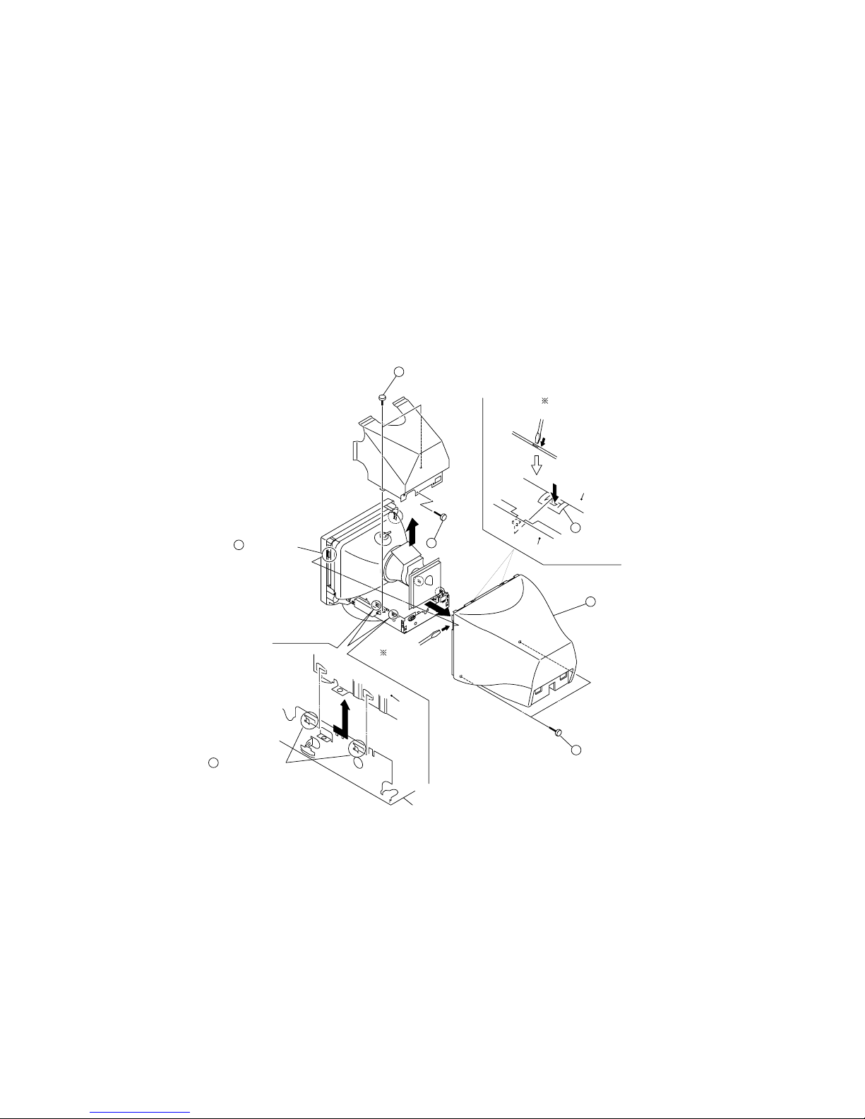
1-1. CABINET ASSEMBLY REMOVAL
6
Two screws
(+BVTP 3x8)
1
Two screws(+BVTP 4x6)
3
Two claws
2
Two claws
4
Cabnet
Cabinet
Bezel
EMI
shield
Base shassis
Push driver into opening
and remove claws.
Push driver into
opening and
remove claws.
5
One scerw
(+BVTP 3x8)
7
Release from
four claws
CPD-G220(E) 1-2
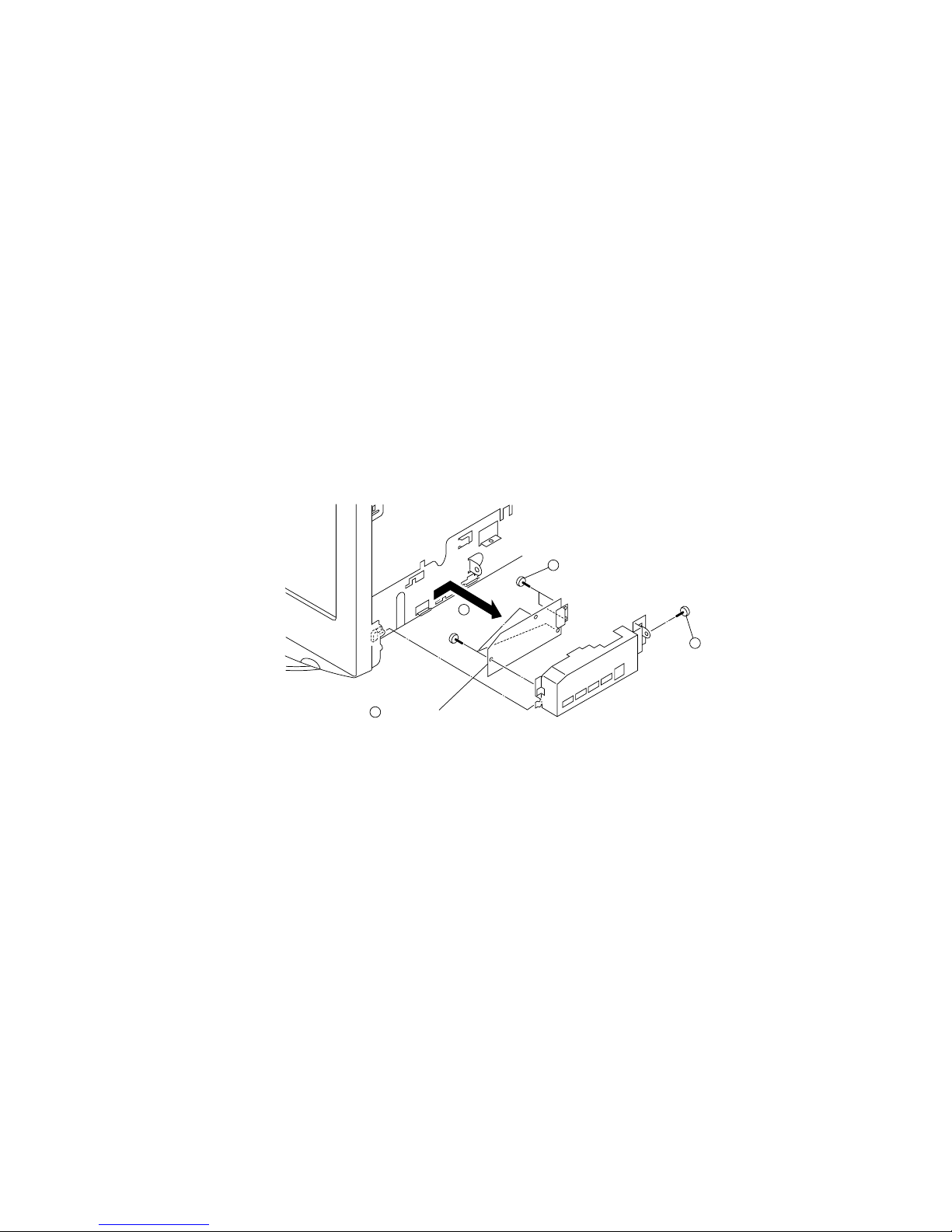
1-2. US BOARD REMOVAL
1
Screw(+BVTP 4x8)
3
Five screws(+BVTT 3x8)
4
US board
2
CPD-G220(E) 1-3
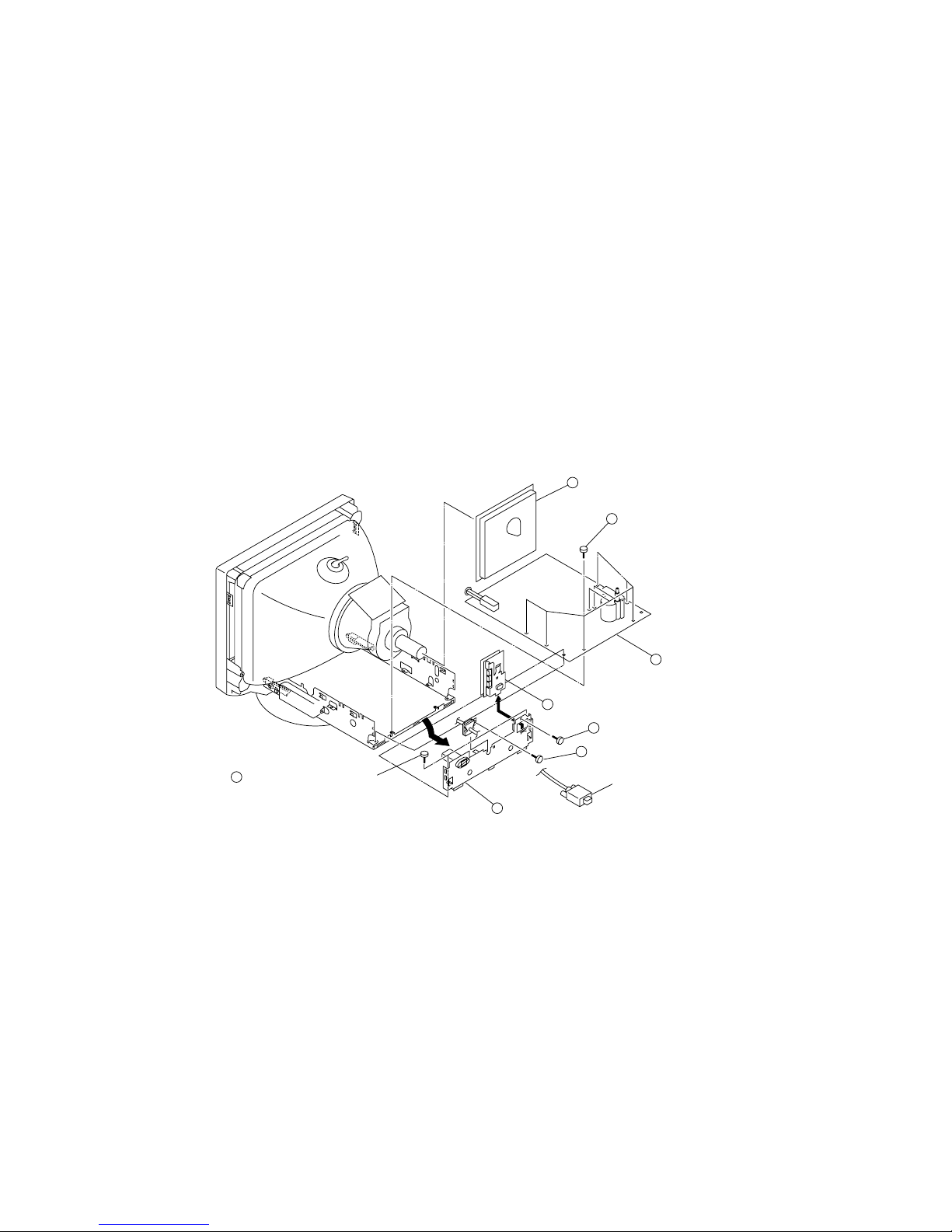
1-3. A, M AND D BOARDS REMOVAL
2
Screws (+BVTP 3x8)
1
Screw (+BVTP 3x8)
5
Cable holder
7
Eight screws (+BVTP 3x8)
4
Two screws (+BVTP 3x8)
3
M board
6
A board
8
D board
Cable assy

CPD-G220(E) 1-4
1-4. SERVICE POSITION
D board
2
1
3
A board
CPD-G220(E) 1-5
1-5. H1 BOARD REMOVAL
1
Three screws (+BVTP 3x8)
2
H1 board
Picture tube
Bezel
Cushion
4
Input button
3
Joystick
CPD-G220(E) 1-6
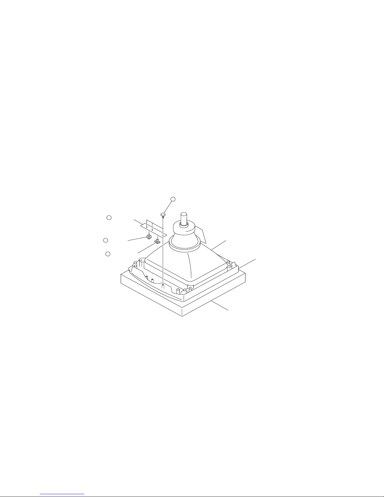
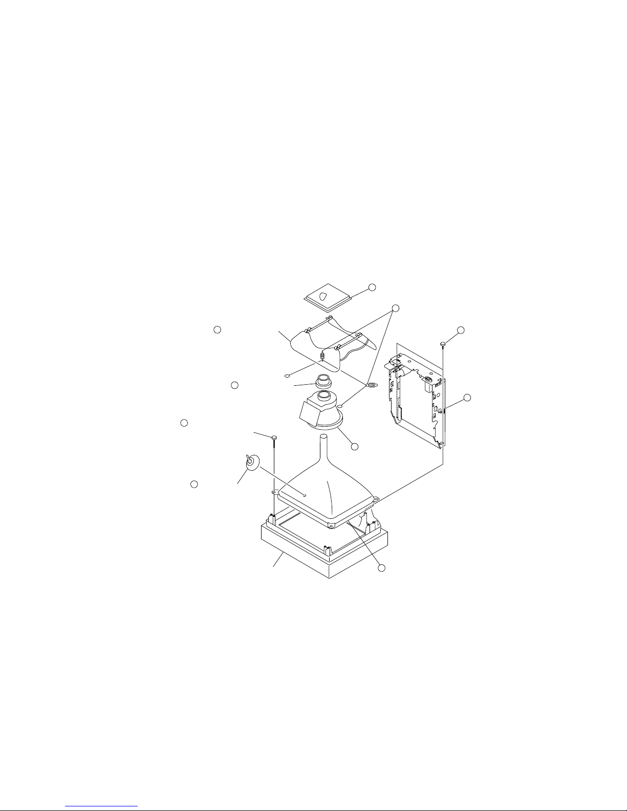
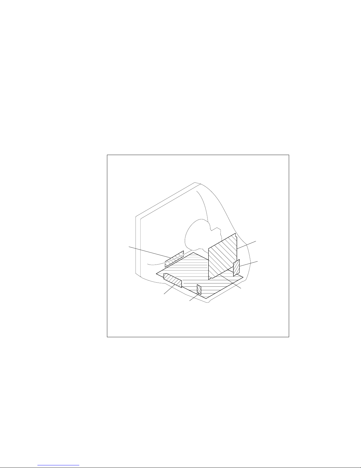
1-6. PICTURE TUBE REMOVAL
1
Anode cap
8
Two extention spring
9
Neck assembly
6
Picture tube
10
Deflection yoke
5
Four screws
(Tapping screw 5)
7
Degaussing coil
2
A board
3
Two screws
(+BVTP 4x16)
4
Base chassis assembly
Cushion
CPD-G220(E) 1-7
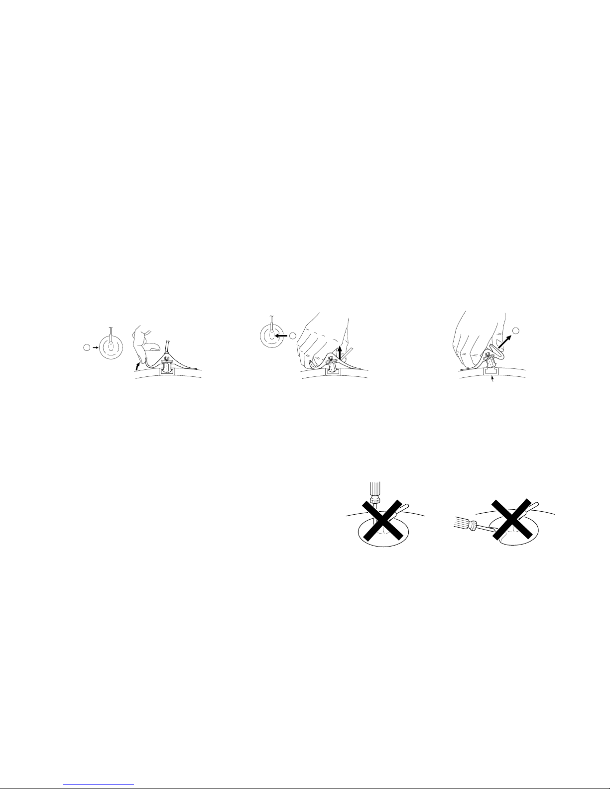
3When one side of the rubber cap is
separated from the anode button, the
anode-cap can be removed by turning up
the rubber cap and pulling up it in the
direction of the arrow c.
•HOW TO HANDLE AN ANODE-CAP
1Don’t scratch the surface of anode-caps with sharp shaped
material!
2Don’t press the rubber hardly not to damage inside of anode-
caps!
A material fitting called as shatter-hook terminal is built in the
rubber.
3Don’t turn the foot of rubber over hardly!
The shatter-hook terminal will stick out or damage the rubber.
•REMOVAL OF ANODE-CAP
NOTE: Short circuit the anode of the picture tube and the anode cap to the metal chassis, CRT shield or carbon painted on the CRT, after
removing the anode.
•REMOVING PROCEDURES
1Turn up one side of the rubber cap in the
direction indicated by the arrow a.
2Using a thumb pull up the rubber cap
firmly in the direction indicated by the
arrow b.
a
b
c
Anode Button
CPD-G220(E) 2-1
Part Replaced ([)
RV501
SECTION 2
SAFETY RELATED ADJUSTMENT
When replacing or repairing the shown below table, the following
operational checks must be performed as a safety precaution against X-rays
emissions from the unit.
* Confirm one minute after turning on the power.
• HV Protector Circuit Check
Using an external DC Power Supply, apply the voltage shown below
between cathode of D517 on D board and GND, and confirm that the
HV HOLD DOWN circuite works. (TV Raster disappears)
Standard voltage : 35.90
V DC
Check Condition
• Input voltage : 120 ± 2 V AC
• Input signal : Cross hatch (white lines on black) at
69kHz (Primary Mode)
• Beam control : CONT, BRT ; minimum "0 "
• Beam Current Protector Check
An ammeter in series between FBT 11 pin on D board and GND, then,
decrease gradually the resistance of the variable resistor from
maximum to minimum, and confirm that the Beam Current
Protector Circuite works (TV Raster disappears). The current must
be within the range shown below.
• Standard current : 1.55
mA
Check Condition
• Input voltage : 120 ± 2 V AC
• Input signal : Cross hatch (white lines on black) at 69kHz
• Beam control : CONT, BRT ; minimum "0"
+0.00
- 0.01
+0.00
- 0.01
HV ADJ
HV Regulator
Circuit Check
HV Protector
Circuit Check
Beam Current
Protector Circuit
Check
Part Replaced (])
D board IC501, C532, C534,
C539, C553, C554,
C555, C556, C558,
C561, R540, R541,
R542, R544, R564,
R567, R568, RV501,
T501 (FBT)
D board IC607, IC901, D515,
D517, C540, C542,
C544, C951, R510,
R543, R547, R549,
R552, R595,
T501 (FBT)
D board IC605,IC607,IC901,
C535, C541,R545,
R546, R548,R550,
R596, R934,
T501 (FBT)

CPD-G220(E) 2-2
• B+ Voltage Check
Standard voltage : 179.0 ± 3.0 V DC
Check Condition
• Input voltage : 120 V AC
Note :Use NF power supply or make sure that distortion factor is
3% or less.
• Input signal : Cross hatch (White lines on black) at 68.7 kHz
• Beam control : CONT : 255 (max), BRT : 255 (max)

CPD-G220(E) 3-1
SECTION 3
ADJUSTMENTS
•Landing Rough Adjustment
1. Enter the full white signal. (or the full black dots signal)
2. Set the contrast to “CONT”=MAX.
3. Make the screen monogreen.
Note: Off the outputs from R ch and B ch of SG.
4. Reverse the DY, and adjust coarsely the purity magnet so that a green
raster positions in the center of screen.
5. Adjust the "H.CENTER" with the H CENTER Volume .(RV502 on the D
board)
6. Moving the DY forward, adjust so that an entire screen becomes
monogreen.
7. Adjust the tilt of DY, and fix lightly with a clamp.
Note: “TILT” shall be set at 0
•Landing Fine Adjustment
1. Put the set inside the Helmholtz coil.
2. Set the TLH to the Zero position.
3. Receive the single green signal.
4. Demagnetize the CRT surface with the hand degausser , and perform
auto degaussing.
5. Attach the wobbling coil to the designated part of the CRT neck.
6. Attach the sensor of the landing adjustment unit on the CRT surface.
7. Adjust the DY position and purity, and the DY tilt.
8. Fasten DY with screw.
Note:Torque 22 ±2kgcm (2.2 ± 0.2 Nm)
Perform auto degaussing.
Purity Magnet <<Zero Position>>
L/D control specification
± 5 ± 5 ± 5
± 5 ± 5 ± 5
± 5 ± 5 ± 4
Purity magnet position
± 4
CPD-G220(E) 3-2
9. Adjust each top and bottom pins by two wedges and then not swing DY
neck right and left. (When fixing DY with wedges, insert wedges
completely so that the DY does not shake.)
10. Adjust the top and bottom pins with the TB.PIN VR complettely. And
ajust the V.Size simulation.
11. Adjust the V.key (=H.Trapxoid) with the H-Trp VR so that [a] become
equol to the [b]
12. If the corner is not within the standards, adjust disc magnet to satisfy L/
D adjustment standards.
Note:
(1) When necessary to paste magnets more than 2 pieces, be careful that the
convergence and the distortion would be alterable.
(2) Paste within 80 to 120 mm from the DY on the diagonal line of the
magnet.
a
b
cd
"a" and "b" must be equal.
c
d
13. If using the magnet, be sure to demagnetize with the degausser and
check.
14. Remove the sensor and wobbling coil.
15. Fix the purity magnet paisted on the DY with the white pen.Fix it with
the RTV.
•Convergence Rough Adjustment
1. Enter the white crosshatch signal (white lines on black).
2. Adjust roughly the horizontal and vertical convergence at four-pole
magnet.
3. Adjust roughly HMC and VMC at six-pole magnet.
•Convergence Adjustment
< Static convergence >
1. Change the "CONV SW" to 0.
2. Receive the crosshatch of R and B. (on black)
3. Adjust H. STAT and V. STAT with 4 pole magnet.
4. Recieve the white crosshatch signal.(White line on black)
5. Adjust HMC and VMC with the 6 pole magnet.
6. Recieve the crosshatch of R and B. (on black)
Note: Adjust H. STAT and V. STAT in the beggining by 4 pole magnet not
adjust them by register immediately.
CPD-G220(E) 3-3
7. If necessary, the 3-6 procedures.
8. Change the "CONV SW" to 6. then set the following registers to 0.
"YBH_T_HI", "TBH_T_LO"
"YBH_B_HI", "YBH_B_LO"
"VSTAT_T_HI", "VSTAT_T_LO"
"VSTAT_B_HI""VSTAT_B_HI"
9. Adjust the H Static and V Static with the register "HSTAT_HI" and
"VSTAT_HI". (These registers should be within the limit between -40
and +40.)
10. Insert to TLH correction board and correct H. TILT.
11. Adjust XCV with the XCV volume.
12 Adjust YCH with the YCH volume.
13 Adjust V. TILT with the TLV-VR.
14. If necessary, repeat the 1-13 procedures to get the most suitable convergence pattern.
15. Paint lock TLH corection board, neck assy 4, 6 pole magnet and XCV
volume.
Purity Mg
4-pole Mg
6-pole Mg
XCV
YCH
H-Trap
TLH
TLV
TB, Pin VI
4 Pole 6 Pole
[ Neck Assy's Zero Position ]
Purity
B
R
RB
R
B
B
R
R
B B
R
XCV YCH
TLV
TLH
B
A
A
0.20 mm
B
MODE All mode
0.24 mm
•White Balance Adjustmen Specification
(1) 9300K
Part of shadow line
for the right figure.
(2) 5000K
Part of shadow line
for the right figure.
•Convergence Specification
VR
x = 0.283
y = 0.298
0.005
0.005
x = 0.346
y = 0.359
0.005
0.005
CPD-G220(E) 3-4
Connect the communication cable of the computer to the connector located on the D board. Run the service software and then follow the instruction.
IBM AT Computer
as a Jig
1-690-391-211A-1500-819-A
Interface Unit
2
*The parts above ( ) are necessary for DAS adjustment.
1
3
D-sub
(9 Pin [female])
mini Din
(8Pin)
4 Pin
3-702-691-01
Connector Attachment
3
To BUS CONNECTOR
4 Pin 4 Pin
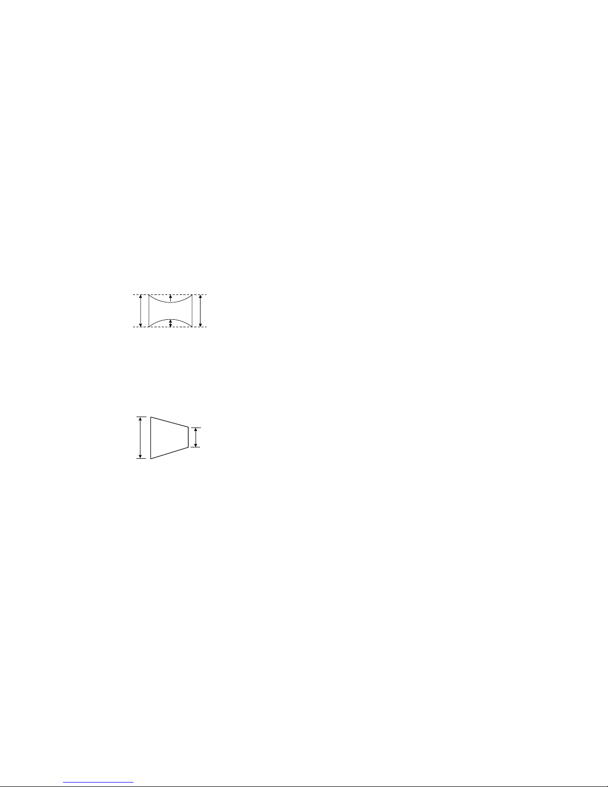
• Vertical and Horizontal Position and Size Specification
• Focus rough adjustment
1. Receive the mE pattern signal. (black characters on green)
2. Adjust the H FOCUS of the screen corner with Fcous VR in the bottom
of the FBT.
3. Receive the cross-hatch pattern signal .(green line on black)
4. Adjust the V FOCUS of the center and the y-axis with the FOCUS VR
in the top of FBT.
A
312 mm
B
MODE All mode
234 mm
a 1.8 mm
b 1.8 mm
a
B
A
b
FBT
Focus volume 1 (V)
Focus volume 2 (H)
G2 VR
CPD-G220(E) 4-1
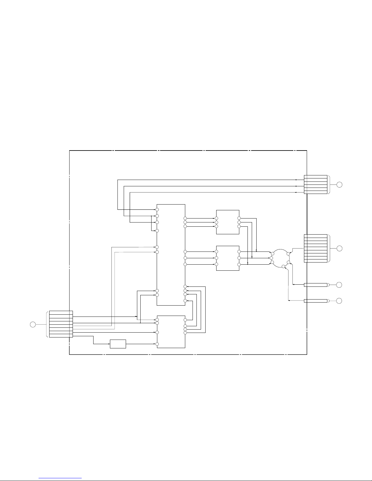
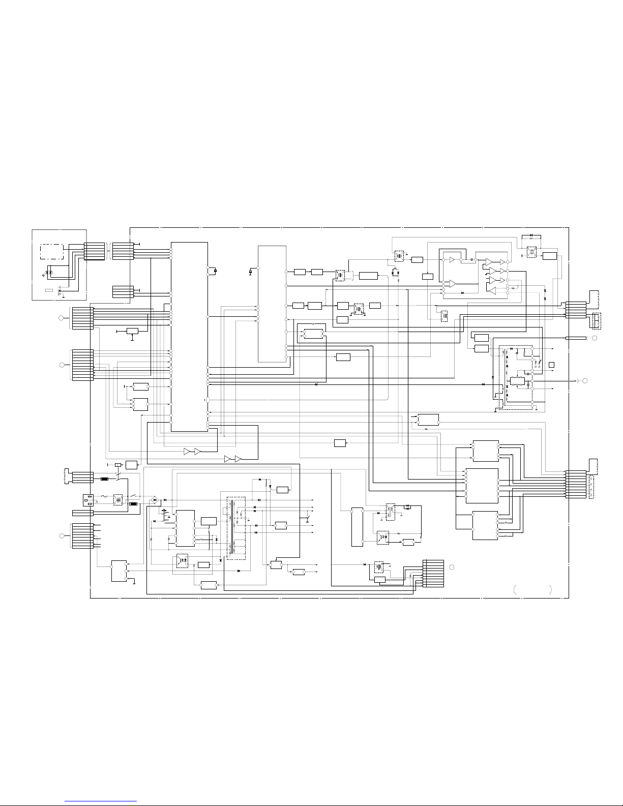
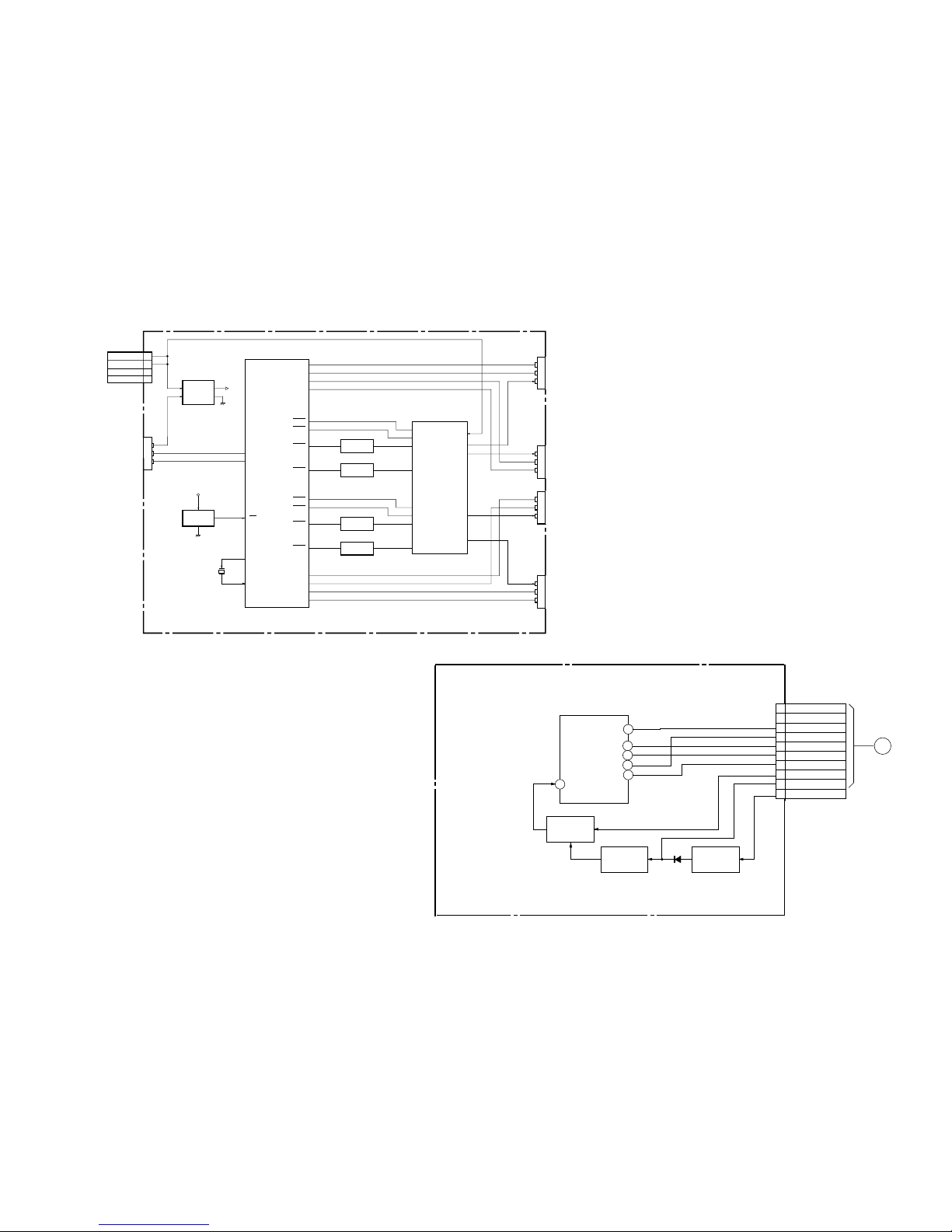
SECTION 4
DIAGRAMS
4-1. BLOCK DIAGRAMS
+180V1
2
3
CN304
NC
+80V
4
GND
5
H1
6
+12V
7
GND
8
+5V
9
STBY +5V
TO
D BOARD
CN606
C
TO
D BOARD
CN512
H
GND1
2
3
CN302
BLUE
GND
4
GREEN
5
GND
6
RED
TO
M BOARD
CN803
A
1
1.2KV
CN301
11
9
8
1
3
5
IC002
VIDEO OUTPUT
J001
B OUT
G OUT
R OUT
B IN
G IN
R IN
KB
KG
KR
G2
H
7
9
11
10
27
24
20
IC001
RGB PRI AMP
B OUT
G OUT
R OUT
3
B BKG
4
G BKG
5R BKG
13B OSD
14G OSD
15 R OSD
17 OSD BLK
B IN
G IN
R IN
SYNC IN
1
SDA
2
SCL
18
BLK
12
CLAMP
7
8
10
12
15
14
OSD BLK
R OSD
G OSD
13 B SOD
SDA
SCL
V FLB
5
H FLB
5
4
3
9
8
7
IC004
RGB CUT - OFF AMP
IC003 OSD
B OUT
G OUT
R OUT
B IN
G IN
R IN
TO
D BOARD
CN902
D
6
5
4
3
IIC SDA
IIC SCL
BPCLP
INV.
Q006
CBLK
2
VR TRC
1
HR TRC
9
8
7
4
10
(VIDEO OUTPUT, OSD)
A
7
8
GND
NC
CN309
TO
D BOARD
CN510
E
1
G1
CN306
G1
3
CPD-G220(E) 4-2
1
3
4
CN801
B GND 1
G GND 1
2
BLUE 1
GREEN1
5
R GND 1
6
RED 1
7
GND
8
VD 1
9
HD 1
SIGNAL IN
HD15
(PIG-TAIL)
13
14
11
12
15
9
10
7
6
8
3
4
1
2
5
3
4
1
2
5
9
10
7
6
8
13
14
11
12
15
25
2
4
28
31
IC801INPUT SELECT
B1
R OUTPUT
G OUTPUT
B OUTPUT
G1
6
R1
7
11
13
V1
(INPUT SELECT)
M
8
H1
19
G.SYNC
21
18
CN802
1
2
3
4
5
6
7
8
9
10
11
12
13
14
15
B2
G2
R2
10
12
14
12 1 213
IC861(2/6)
INVERTER
+
+
-
45 63
IC861(2/6)
INVERTER
5
7
6
V CLK
IC831
EEP ROM
SDA
SCL
2
3
BLUE
1
RED
CN803
G GND
4
GREEN
5
R GND
6
B GND
TO
A BOARD
CN302
2
3
DDC SDA1
1
HOST GND1
CN805
DDC SCL1
4
STAND-BY +5V
5
GND
6
HSYNC
7
YSYNC
8
CSYNC
9
HOST GND2
10
INPUT SEL SW
11
POWER SW
TO
D BOARD
CN903
H OUT
V OUT
7
6
5
V CLK
IC802
EEP ROM
SCL
SDA
1
3
CN804
HOST 5V1
DDC SDA1
2
DDC SCL1
4
HOST GND 1
V215
H2
16
A
B
POWER SAVE
SW
CPD-G220(E) 4-3
6
4
3
5
2
1
STBY 5V
CN1001
1
2
3
GND
KEY
4
LED RED
5
LED GRN
D1005
S1007,1003
KEY MATRIX
PB4
X901
24MHz
SDA
SCL
H IN
V IN
X5
PA5
PA6
PB5
RDI
CBLK
CLP
SCL
SDA
DDC SCL
DDC SDA
PC1
PB7
PB6
DA4
RESET
DA8
DA6
V IN
OOB
10
11
12
13
14
15
16
17
18
1
OUT
2
DA5
TDO
OSC OUT
OSC IN
HSO
ITA
HFB
DA3
PFV
PB1
PB3
DA1
DRIVER
7
6
5
4
1
2
4
CTL
VCC
VADJ
3
VCRL
I SENSE
IREF
DS
GND
DEM
V AUX
H OUT
H FLY
V SAW
V SIN
V DIV
LOCK
V DF
E/W
X902
CN904
S1006
SELECT
IC901 CPU
IC902 DEF CONTR0L
STBY 5V
GND
KEY
LED RED
INPUT SEL SW
1
3
4
2
5
6
7
8
HRTRC
VRTRC
CBLK
BPCLP
IICSCL
GND
IISDA
CSYNC
1
3
4
2
5
6
7
8
9
+180V
CN606
IC602
HEATER OUT
NC
+80V
GND
H1
+12V
GND
+5V
SRBY +5V
1
3
4
2
5
6
7
8
9
HOST GND1
CN903
DDC SDA1
HOST GND1
HOST 5V/STBY 5V
GND
HSYNC
VSYNC
CSYNC
HOST GND2
10
INPUT SEL SW
1
3
4
2
D GND
CN902
IC904 RESET
RY601
+12V
RELAY
DRIVE
Q601
TH601
F601
S601
TH600
D609
D620
D605
IC604 ERROR AMP
D619
IC605
+12V REG
IC608
+5V REG
D622
D614
D618
D617
D611
D613
IC607
+5V REG
D612
LF602
LFT
D601
AC RECT
IC601
SW REG CONT
IC603
POWER
SWITCHING
Q602
CN600
IC905 EEPROM
STBY
+5V
CN901
STBY +5V
RXD
TXD
1
3
L43
12
G
N
+180V
+80V
+12V
+5V-4
STBY +5V
+5V-4
+12V
-15V
STBY +5V
+15V
+80V
+180V
2
DGC 2
NC
DGC 1
2
1
THP600A
CN602
CN601
THP600
G11
5
4
NC
6
H DY+
H -DY
V-DY
CN501
CN510
H DY-
3
NC
2
V DY-
1
V DY+
ROTATION+
CY-DY
CN701
ROTATION
1
2
3
ROTATION-
CY1+
4
CY1-
5
CY2+
6
CY2-
7
CY3+
8
CY3-
9
CY4+
10
CY4-
15
48
47
44
45
38
39
46
22
36
37
34
35
33
12
13
CSI
28
5
54
9
7
8
5
5
7
4
6
6
4
I O
I O
5
7
6
13
11
3 1
I O
8
1
2
4
5
9
14
2
DA2
OUT
WC
AC IN
DGC
3
16
18
19
4
32
23
27 26
4
3
29
12
64
82
64
52
31
1
3
81
9
17
14
8 1 5
7 3
3
23
2
8
4
10
27
2
28
24 22
20
19
18
13
14
12
HV
13
16
FV1
15
14
FV2
12
1
6
54
16
17
14
2
3
5
4 3
1
2
76
9
8
9
8
7
6
2
10
3
1
1
2 4
BUFF
Q505
DF AMP
Q504
H DRIVE
Q501,502
H DRIVE
OUT
Q511
S-CAP CHANGE
Q512-516
H OUT
Q507
L503
HOC
BUFF
+
+
+
-
-
-
+
+
IC501 PWM CONTROL
AMP
REF
RV501
HV
ADJ
ABL
D515
D522
D523
TO
PICTURE TUBE
FOCUS
FOCUS
HV REG OUT
Q510
CHOPPER
Q503
T501 FBT
2
1
7
6
SYNC LOCK
Q522, 524
D517
H FLY
BUFF
Q525
S0-S4
IC502 ROTATION DRIVE
IC702
D CONVERGENCE OUT
IC701 CONVERGENCE CONTROL
IC703
S CONVERGENCE OUT
T504
HDT
T503
DFT
T505
HST
BUFF
Q521
H REG
Q520
S0-S4
H BLK
BUFF
Q508
H AMP
Q903
IC401 V OUT
OUT
OUT
STBY5V
OUT B
-IN B
OUT A
-IN A
V CONV OUT
H CONV OUT
H STATIC OUT
V STATIC OUT
-IN A
I OUT A
OUT A
-IN B
I OUT B
OUT B
FB
-IN
+IN
+IN
STBY
+IN B
+IN A
SDA
SCL
HD IN
VS IN
V POS IN
V REF OUT
+IN A
+IN B
+IN
VCC
VCC
SDA
SCL
49
53
PA0
PA4
OVP/OCP
Q604
T601
SRT
REG SW
Q603
CONVERGENCE CONTROL,
DEFLECTION, CPU,
POWER SUPPLY
D
TO
A BOARD
CN306
E
TO
A BOARD
CN304
C
TO
A BOARD
CN309
D
TO
M BOARD
CN805
B
(USER CONTROL, LED)
H1
11
14
6
INPUT SEL SW
LED GREEN
STBY 5V
STBY 5V
VSD
26
PD3
25
11
POWER SW
PD4
24
BUFF
Q901
+5V
+12V
12 11 1013
IC908(2/2)
INVERTER
13 41
IC908(2/2)
INVERTER
VSI1
20
HSI1
30
4
10
D628
S602
Q605,612
4
D510
LF506
LCT
710
25
+12V
D505
L508/HLC
CHOPPER
Q509
RV502
L510
HCC
D531
D530
18
2
5
T602
SRT
1
2
4
3
PH601
IC611
3 1
3
1
7
IC610
D633
D634
3
4
M
D
C
GND
CN603
1
2
3
GND
DRIVE
4
I SENSE
5
V SENSE
6
AC SENSE
7
L SENSE
8
VCC
9
LVP
10
OVP
TO DP BOARD
CN1600
1
9
8
L654
AFT
3
D629
OVP/OCP
Q607
9
G
TO
A BOARD
CN301
H
NC
4
CN512
CPD-G220(E) 4-4
POWER SW
Q2601
IC2602
IC2603
POWER SW
Q2602
POWER SW
Q2603
POWER SW
Q2604
1
2
3
V BUS
D—
D+
CN2901
41
40
37
42
43
3
2
2
6
1
5
10
15
9
14
31
32
10
11
12
12
17
4
8
13
35
36
4
5
7
6
25
24
IVCO
G
DP1
DM1
DM2
DP2
DM0
DP0
DP3
DM3
DM4
DP4
IC2601
5V-REG
O
I
G
IC2902
RESET
X2901
12MHz
5V
IC2901
USB CONT
IC2602
4 OUTPUT VOLTAGE REGULATOR
5V
3
2
1
D+1
D—1
V BUS1
CN2902
D+3
D—3
V BUS3
CN2904
1
2
3
3
2
1
1
2
3
OVR-1
OVR-2
POW-1
POW-2
POW-3
POW-4
OVR-3
OVR-4
V BUS2
C—2
D+2
CN2903
V BUS4
C—4
D+4
CN2905
US
(USB CONTROL)
RST
XIN
XOUT
6.5V
6.5V
CN2601
1
2
FLG1
FLG2
VC1
VC2
VOUT1
VOUT2
FLG3
FLG4
VC1
VC2
VOUT3
VOUT4
TO D BOARD
CN605
1
2
5
3
GND
GND34
V IN
18
GND1
2
3
CN1600
GND
DRIVE
4
I SENSE
5
V SENSE
6
AC SENSE
7
L SENSE
8
VCC
9
LVP
TO
D BOARD
CN603
G
8
1
3
4
IC1600
V SENSE
AC SENSE
I SENSE
VCC
5
7
L SENSE
DRIVE
(PFC CONTROL)
DP
10 OVP
AMP
Q16031602
INV.
Q1601
INV.
Q1600
D1600

CPD-G220(E) 4-5
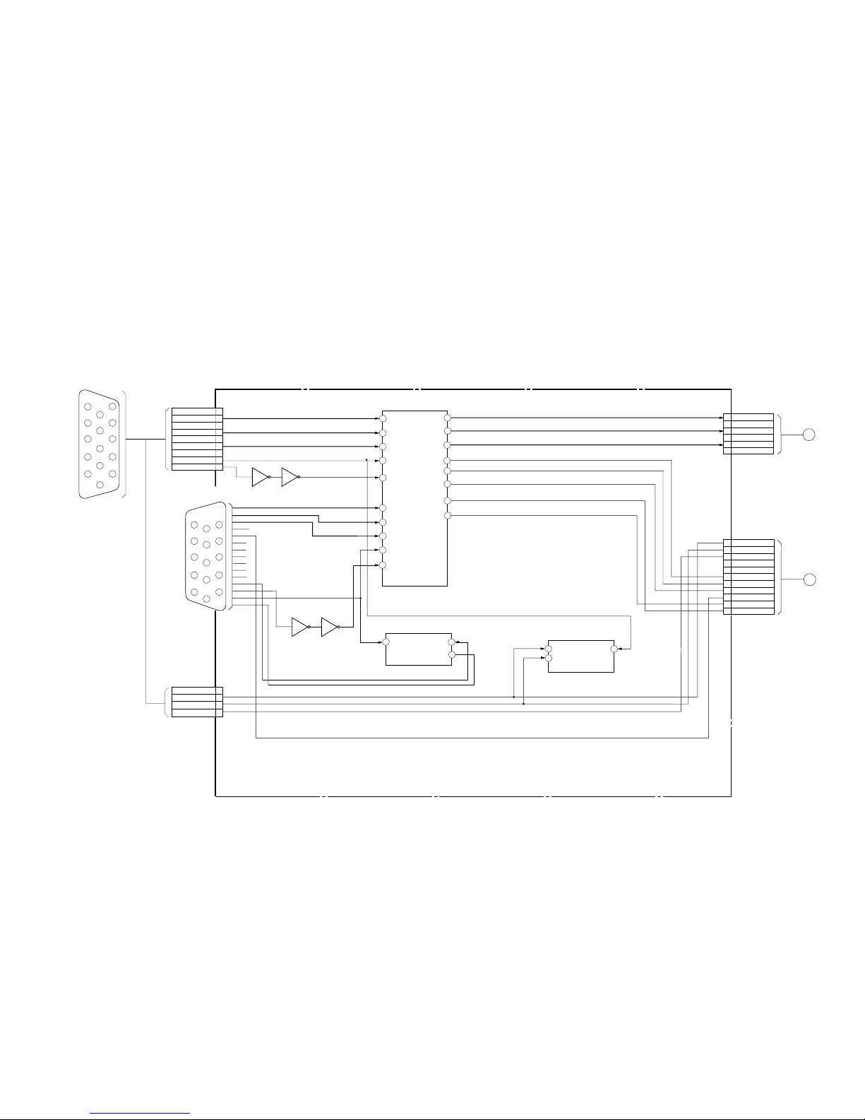
4-2. FRAME SCHEMATIC DIAGRAM
AC IN
D
HV
DEFLECTION,CPU,
CONVERGENCE CONTROL,
POWER SUPPLY
B-SS3572<J..>-KESSENZU
H
G1
G2
HG
RGB
PICTURE
TUBE
G1
1
1 1.2KV
CN903
11P
11
10
987654321
POWER SW
INPUT SEL SW
HOST GND2
CSYNC
VSYNC
HSYNC
GND
STAND-BY 5V
DDC SCL1
DDC SCA1
HOST GND1
CN801
9P
11
10
987654321
POWER SW
INPUT SEL SW
HOST GND2
CSYNC
VSYNC
HSYNC
GND
HOST 5V/STBY 5V
DDC SCL1
DDC SCA1
HOST GND1
CN309
7P
8765432
1
NC
IICSDA
GND
IICSCL
BPCLP
CBLK
VRTRC
HRTRC
CN304
9P
WHT
987654321
STBY 5V
+5V
GND
+12VH1GND
+80VNC+180V
CN606
9P
WHT
987654321
STBY 5V
+5V
GND
+12V
H1
GND
+80V
NC
+180V
CN605
4P
WHT
:S-MICRO
CN902
7P
8765432
1
NC
IICSDA
GND
IICSCL
BPCLP
CBLK
VRTRC
HRTRC
M
H1
US
(
USB CONTROL
)
DP
A
CN1600
10P
10
9
8
7
6
5
4
3
2
1
CN502
40P
10
9
8
7
6
5
4
3
2
1
DVP
LVP
VCC
L SENSE
AC SENSE
V SNESE
I SENSE
DRIVE
GND
GND
CN904
8P
65432
1
STBY 5V
GND
KEY
LED RED
LED GRN
INPUT SEL SW
CN1001
6P
12345
6
STBY 5V
GND
KEY
LED RED
LED GRN
INPUT SEL SW
1
2
3
4
5
6
7
8
9
10
ROTATION+
ROTATION—
CY1+
CY1CY2+
CY2CY3+
CY3CY4+
CY4-
CN701
10P
WHT
:S-MICRO
ROTATION
V DY
H DY
CN501
6P
WHT
:VH
1
2
3
4
5
6
V DY+
V DY—
NC
H DY—
NC
H DY+
DGC
1
2
3
4
DGC4
NC
NC
DGC1
CN601
4P
CN600
3P
1
2
3
AC L
NC
AC N
1
2
3
4
D GND
+5V
RXD
TXD
CN901
4P
S-MICRO
TO ECS
CN2601
4P
1
2
3
4
6.5V
6.5V
GND
GND
CN802
5
4
3
2
1
10
9
8
7
6
15
14
13
12
11
SIGNAL IN
HD-15
(PIG-TAIL)
1
2
3
4
5
6
B.GND
BLUE
G.GND
GREEN
R.GND
RED
CN803
6P
DVP
LVP
VCC
L SENSE
AC SENSE
V SNESE
I SENSE
DRIVE
GND
GND
1
2
3
4
6.5V
6.5V
GND
GND
6
5
4
3
2
1
B.GND
BLUE
G.GND
GREEN
R.GND
RED
987654321
HD1
VD1
GND
RED1
R.GND1
GREEN1
G.GND1
BLUE1
B.GND1
CN805
11P
CN302
6P
CN510
1P
CN804
4P
432
1
HOST GND 1
DDC SDA1
DDC SCL1
HOST 5V1
CN301
1P
1 G1
CN306
1P
(INPUT SELECT)
(
VIDEO OUTPUT, OSD
)
(
USER CONTROL, LED
)
1
2
3
4
5
678910
11
12
13
14
15
SIGNAL IN
HD-15
CN603
10P
(PFC CONTROL)
CN512
1P
CPD-G220(E) 4-6
4-3. CIRCUIT BOARDS LOCATION
A
D
US
H1
M
DP
 Loading...