

Page 1

TMR-RF940R
SERVICE MANUAL
TMR-RF940R is transmitter
unit in MDR-RF940RK.
SPECIFICATIONS
AEP Model
MICROFILM
TRANSMITTER
Page 2

Notes on chip component replacement
• Never reuse a disconnected chip component.
• Notice that the minus side of a tantalum capacitor may be dam-
aged by heat.
Flexible Circuit Board Repairing
• Keep the temperature of the soldering iron around 270 ˚C during
repairing.
• Do not touch the soldering iron on the same conductor of the
circuit board (within 3 times).
• Be careful not to apply force on the conductor when soldering or
unsoldering
This section is extracted from
instruction manual.
SECTION 1
GENERAL
– 2 –
Page 3
SECTION 2
y
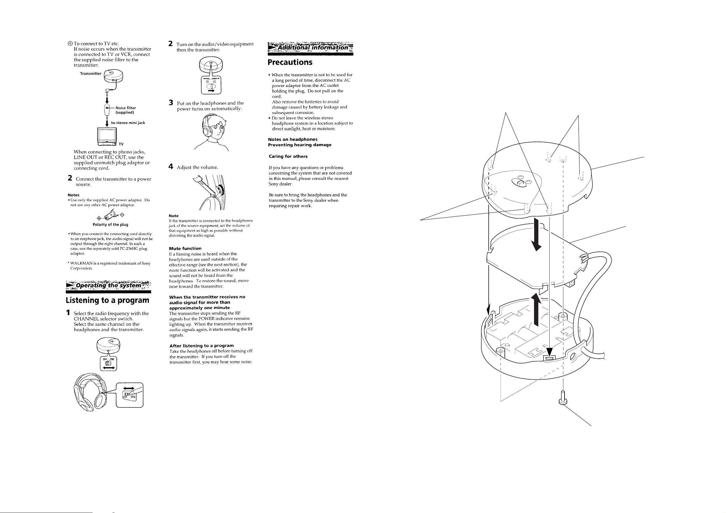
DISASSEMBLY
Note: Follow the disassembly procedure in the numerical order given.
CABINET (UPPER) ASS’Y
2
two claws
4
two claws
3
cabinet (upper) ass’
4
two claws
5
TX board
– 3 –
– 4 –
1
two screws
(P2.6
×
10)
Page 4

Page 5

Page 6

NOTE:
• -XX and -X mean standardized parts, so they
may have some difference from the original
one.
• Color Indication of Appearance Parts
Example:
KNOB, BALANCE (WHITE) . . . (RED)
↑↑
Parts Color Cabinet's Color
4
SECTION 4
EXPLEDED VIEW
• Items marked “*” are not stocked since they
are seldom required for routine service. Some
delay should be anticipated when ordering these
items.
• The mechanical parts with no reference number in the exploded views are not supplied.
TX
NOTE:
• Due to standardization, replacements in the
parts list may be different from the parts specified in the diagrams or the components used
on the set.
• -XX and -X mean standardized parts, so they
may have some difference from the original
one.
• RESISTORS
All resistors are in ohms.
METAL: Metal-film resistor.
METAL OXIDE: Metal oxide-film resistor.
SECTION 5
ELECTRICAL PARTS LIST
F: nonflammable
• Items marked “*” are not stocked since they
are seldom required for routine service.
Some delay should be anticipated when ordering these items.
• SEMICONDUCTORS
In each case, u: µ, for example:
uA. . : µA. . uPA. . : µPA. .
uPB. . : µPB. . uPC. . : µPC. .
uPD. . : µPD. .
• CAPACITORS
uF: µF
• COILS
When indicating parts by reference
number, please include the board.
15
3
2
14
not supplied
1
12
11
Ref. No. Part No. Description Remark
1 3-895-784-01 SPRING
2 4-957-332-01 CABINET (LOWER)
* 3 A-4542-442-A TX BOARD, COMPLETE
4 X-4948-054-1 CABINET (UPPER) ASSY
5 1-559-892-11 CORD (WITH PLUG)
6 4-958-633-01 CUSHION (BATTERY CASE LID)
7 4-957-333-01 LID, BATTERY CASE
8 7-685-135-19 SCREW +P 2.6X10 TYPE2 NON-SLIT
15
not supplied
5
6
13
8
not supplied
10
Ref. No. Part No. Description Remark
9 4-987-337-01 LABEL (CHG), WARNING
10 4-989-335-01 TERMINAL, CHARGE
11 4-986-508-01 COVER (BATTERY CASE)
12 4-989-336-01 TERMINAL (COMMONNESS), CHARGE
13 3-846-312-01 SPACER
14 3-561-902-01 CLOTH, RETAINING, CASSETTE
15 3-880-474-01 CUSHION, 15X5X0.3
Ref. No. Part No. Description Remark
* A-4542-442-A TX BOARD, COMPLETE
C01 1-163-141-00 CERAMIC CHIP 0.001uF 5% 50V
C02 1-163-037-11 CERAMIC CHIP 0.022uF 10% 25V
C03 1-128-007-11 ELECT CHIP 2.2uF 20% 35V
C11 1-163-141-00 CERAMIC CHIP 0.001uF 5% 50V
C12 1-163-037-11 CERAMIC CHIP 0.022uF 10% 25V
C13 1-128-007-11 ELECT CHIP 2.2uF 20% 35V
C21 1-107-823-11 CERAMIC CHIP 0.47uF 10% 16V
C22 1-164-489-11 CERAMIC CHIP 0.22uF 10% 16V
C23 1-163-131-00 CERAMIC CHIP 390PF 5% 50V
C24 1-163-131-00 CERAMIC CHIP 390PF 5% 50V
C31 1-163-135-00 CERAMIC CHIP 560PF 5% 50V
C32 1-163-141-00 CERAMIC CHIP 0.001uF 5% 50V
C41 1-128-393-11 ELECT CHIP 100uF 20% 10V
C42 1-164-222-11 CERAMIC CHIP 0.22uF 25V
9
7
C43 1-126-246-11 ELECT CHIP 220uF 20% 4V
C44 1-126-205-11 ELECT CHIP 47uF 20% 6.3V
C45 1-126-205-11 ELECT CHIP 47uF 20% 6.3V
C51 1-164-489-11 CERAMIC CHIP 0.22uF 10% 16V
C52 1-164-695-11 CERAMIC CHIP 0.0022uF 5% 50V
C53 1-163-141-00 CERAMIC CHIP 0.001uF 5% 50V
C54 1-163-251-11 CERAMIC CHIP 100PF 5% 50V
C55 1-163-116-00 CERAMIC CHIP 91PF 5% 50V
C56 1-163-251-11 CERAMIC CHIP 100PF 5% 50V
C57 1-164-232-11 CERAMIC CHIP 0.01uF 50V
C58 1-163-116-00 CERAMIC CHIP 91PF 5% 50V
C59 1-163-251-11 CERAMIC CHIP 100PF 5% 50V
C60 1-164-232-11 CERAMIC CHIP 0.01uF 50V
C61 1-163-241-11 CERAMIC CHIP 39PF 5% 50V
C62 1-163-243-11 CERAMIC CHIP 47PF 5% 50V
C63 1-164-232-11 CERAMIC CHIP 0.01uF 50V
C64 1-163-112-00 CERAMIC CHIP 62PF 5% 50V
C65 1-163-108-00 CERAMIC CHIP 43PF 5% 50V
C66 1-163-059-91 CERAMIC CHIP 0.01uF 10% 50V
C67 1-163-089-00 CERAMIC CHIP 6PF 50V
C68 1-163-088-00 CERAMIC CHIP 5PF 50V
C69 1-164-232-11 CERAMIC CHIP 0.01uF 50V
C70 1-163-094-00 CERAMIC CHIP 11PF 5% 50V
C71 1-163-096-00 CERAMIC CHIP 13PF 5% 50V
C72 1-164-232-11 CERAMIC CHIP 0.01uF 50V
C73 1-163-092-00 CERAMIC CHIP 9PF 0.25PF 50V
*******************
< CAPACITOR >
Ref. No. Part No. Description Remark
C74 1-163-091-00 CERAMIC CHIP 8PF 50V
C75 1-164-232-11 CERAMIC CHIP 0.01uF 50V
C76 1-163-091-00 CERAMIC CHIP 8PF 50V
C77 1-163-227-11 CERAMIC CHIP 10PF 0.5PF 50V
C78 1-164-232-11 CERAMIC CHIP 0.01uF 50V
C79 1-164-232-11 CERAMIC CHIP 0.01uF 50V
C80 1-163-094-00 CERAMIC CHIP 11PF 5% 50V
C81 1-163-227-11 CERAMIC CHIP 10PF 0.5PF 50V
C82 1-164-232-11 CERAMIC CHIP 0.01uF 50V
C83 1-163-091-00 CERAMIC CHIP 8PF 50V
C84 1-163-090-00 CERAMIC CHIP 7PF 50V
C85 1-163-229-11 CERAMIC CHIP 12PF 5% 50V
C86 1-164-232-11 CERAMIC CHIP 0.01uF 50V
C87 1-163-229-11 CERAMIC CHIP 12PF 5% 50V
C88 1-163-083-00 CERAMIC CHIP 1PF 50V
C89 1-163-087-00 CERAMIC CHIP 4PF 50V
C90 1-104-908-11 TANTALUM CHIP 47uF 20% 4V
C91 1-163-038-91 CERAMIC CHIP 0.1uF 25V
C92 1-163-113-00 CERAMIC CHIP 68PF 5% 50V
C93 1-163-038-91 CERAMIC CHIP 0.1uF 25V
C94 1-164-232-11 CERAMIC CHIP 0.01uF 50V
C95 1-163-037-11 CERAMIC CHIP 0.022uF 10% 25V
C96 1-164-232-11 CERAMIC CHIP 0.01uF 50V
C97 1-135-158-21 TANTALUM CHIP 15uF 20% 4V
C98 1-163-141-00 CERAMIC CHIP 0.001uF 5% 50V
C100 1-107-725-11 CERAMIC CHIP 0.1uF 10% 16V
< DIODE >
D41 8-719-404-49 DIODE MA111
D42 8-719-975-06 LED CL-70G-CD (OFF/CHG)
D43 8-719-018-51 LED CL-170R-CD (POWER ON)
D44 8-719-045-99 DIODE RD2.2M-T1B
D51 8-719-939-02 DIODE SVC203CP
D52 8-719-421-40 DIODE MA77
D53 8-719-421-40 DIODE MA77
< FERRITE BEAD >
FB01 1-500-419-21 INDUCTOR, FERRITE BEAD
< IC >
IC01 8-759-998-71 IC BA3308F
IC21 8-759-701-39 IC NJM3404AM
IC22 8-759-177-69 IC TLV2362ID-ELL2500
– 9 –
– 10 –
Page 7

TX
Ref. No. Part No. Description Remark
< JACK >
J41 1-568-907-31 JACK,DC (POLARITY UNIFEID TYPE)
(DC IN 4.5V)
< CHIP CONDUCTOR >
JC01 1-216-296-00 CONDUCTOR, CHIP (3216)
JC02 1-216-296-00 CONDUCTOR, CHIP (3216)
JC03 1-216-296-00 CONDUCTOR, CHIP (3216)
JC04 1-216-296-00 CONDUCTOR, CHIP (3216)
JC05 1-216-296-00 CONDUCTOR, CHIP (3216)
JC06 1-216-296-00 CONDUCTOR, CHIP (3216)
JC07 1-216-295-00 CONDUCTOR, CHIP (2012)
JC08 1-216-295-00 CONDUCTOR, CHIP (2012)
< COIL >
L51 1-412-946-11 INDUCTOR ,CHIP 3.9uH
L52 1-412-948-11 INDUCTOR ,CHIP 5.6uH
L53 1-412-946-11 INDUCTOR ,CHIP 3.9uH
L66 1-416-385-11 COIL, AIR-CORE (TMR)
L67 1-416-385-11 COIL, AIR-CORE (TMR)
L68 1-416-385-21 COIL, AIR-CORE (TMR)
L69 1-416-385-21 COIL, AIR-CORE (TMR)
L70 1-412-925-11 INDUCTOR ,CHIP 68NH
L71 1-412-946-11 INDUCTOR ,CHIP 3.9uH
L72 1-412-946-11 INDUCTOR ,CHIP 3.9uH
< LINE FILTER >
LF01 1-403-601-21 FILTER, COMMON MODE
LF41 1-411-236-11 FILTER, EMI
LF42 1-411-236-11 FILTER, EMI
< TRANSISTOR/CHIP CONDUCTOR >
Q21 8-729-200-63 TRANSISTOR 2SC2712L-TE85R
Q22 8-729-200-63 TRANSISTOR 2SC2712L-TE85R
Q23 8-729-200-63 TRANSISTOR 2SC2712L-TE85R
Q24 8-729-216-22 TRANSISTOR 2SA1162-G
Q25 8-729-200-63 TRANSISTOR 2SC2712L-TE85R
Q31 8-729-200-63 TRANSISTOR 2SC2712L-TE85R
Q43 8-729-200-63 TRANSISTOR 2SC2712L-TE85R
Q44 8-729-200-63 TRANSISTOR 2SC2712L-TE85R
Q45 8-729-200-63 TRANSISTOR 2SC2712L-TE85R
Q46 8-729-200-87 TRANSISTOR 2SC2714-Y
Q47 8-729-200-87 TRANSISTOR 2SC2714-Y
Q48 8-729-209-45 TRANSISTOR 2SC3120-TE85R
Q49 8-729-230-81 TRANSISTOR 2SC3606
Q50 8-729-230-81 TRANSISTOR 2SC3606
Q51 8-729-230-81 TRANSISTOR 2SC3606
Q52 8-729-216-22 TRANSISTOR 2SA1162-G
< RESISTOR/CHIP CONDUCTOR >
R01 1-216-085-00 METAL CHIP 33K 5% 1/10W
R02 1-216-049-00 METAL CHIP 1K 5% 1/10W
Ref. No. Part No. Description Remark
R03 1-216-061-00 METAL CHIP 3.3K 5% 1/10W
R04 1-216-097-00 METAL CHIP 100K 5% 1/10W
R05 1-216-061-00 METAL CHIP 3.3K 5% 1/10W
R06 1-216-033-00 METAL CHIP 220 5% 1/10W
R07 1-216-061-00 METAL CHIP 3.3K 5% 1/10W
R08 1-216-061-00 METAL CHIP 3.3K 5% 1/10W
R11 1-216-085-00 METAL CHIP 33K 5% 1/10W
R12 1-216-049-00 METAL CHIP 1K 5% 1/10W
R13 1-216-061-00 METAL CHIP 3.3K 5% 1/10W
R14 1-216-097-00 METAL CHIP 100K 5% 1/10W
R15 1-216-061-00 METAL CHIP 3.3K 5% 1/10W
R16 1-216-033-00 METAL CHIP 220 5% 1/10W
R17 1-216-061-00 METAL CHIP 3.3K 5% 1/10W
R18 1-216-073-00 METAL CHIP 10K 5% 1/10W
R21 1-216-073-00 METAL CHIP 10K 5% 1/10W
R22 1-216-061-00 METAL CHIP 3.3K 5% 1/10W
R23 1-216-057-00 METAL CHIP 2.2K 5% 1/10W
R24 1-216-057-00 METAL CHIP 2.2K 5% 1/10W
R25 1-216-093-00 METAL CHIP 68K 5% 1/10W
R26 1-216-085-00 METAL CHIP 33K 5% 1/10W
R27 1-216-081-00 METAL CHIP 22K 5% 1/10W
R28 1-216-081-00 METAL CHIP 22K 5% 1/10W
R29 1-216-057-00 METAL CHIP 2.2K 5% 1/10W
R30 1-216-057-00 METAL CHIP 2.2K 5% 1/10W
R31 1-216-057-00 METAL CHIP 2.2K 5% 1/10W
R32 1-216-061-00 METAL CHIP 3.3K 5% 1/10W
R33 1-216-057-00 METAL CHIP 2.2K 5% 1/10W
R42 1-216-023-00 METAL CHIP 82 5% 1/10W
R43 1-216-009-00 METAL CHIP 22 5% 1/10W
R44 1-216-053-00 METAL CHIP 1.5K 5% 1/10W
R45 1-216-033-00 METAL CHIP 220 5% 1/10W
R49 1-216-133-00 METAL CHIP 3.3M 5% 1/10W
R51 1-216-097-00 METAL CHIP 100K 5% 1/10W
R52 1-216-109-00 METAL CHIP 330K 5% 1/10W
R53 1-216-055-00 METAL CHIP 1.8K 5% 1/10W
R54 1-216-033-00 METAL CHIP 220 5% 1/10W
R55 1-216-097-00 METAL CHIP 100K 5% 1/10W
R56 1-216-033-00 METAL CHIP 220 5% 1/10W
R57 1-216-091-00 METAL CHIP 56K 5% 1/10W
R58 1-216-295-00 CONDUCTOR, CHIP (2012)
R59 1-216-001-00 METAL CHIP 10 5% 1/10W
R60 1-216-001-00 METAL CHIP 10 5% 1/10W
R61 1-216-001-00 METAL CHIP 10 5% 1/10W
R62 1-216-079-00 METAL CHIP 18K 5% 1/10W
R63 1-216-150-00 METAL CHIP 10 5% 1/8W
R64 1-216-001-00 METAL CHIP 10 5% 1/10W
R65 1-216-295-00 CONDUCTOR, CHIP (2012)
R66 1-216-001-00 METAL CHIP 10 5% 1/10W
R67 1-216-077-00 METAL CHIP 15K 5% 1/10W
R68 1-216-295-00 CONDUCTOR, CHIP (2012)
R69 1-216-001-00 METAL CHIP 10 5% 1/10W
R70 1-216-295-00 CONDUCTOR, CHIP (2012)
R71 1-216-001-00 METAL CHIP 10 5% 1/10W
– 11 –
Page 8

TMR-RF940R
TX
Ref. No. Part No. Description Remark
R72 1-216-073-00 METAL CHIP 10K 5% 1/10W
R73 1-216-073-00 METAL CHIP 10K 5% 1/10W
R74 1-216-295-00 CONDUCTOR, CHIP (2012)
R75 1-216-017-00 METAL CHIP 47 5% 1/10W
R76 1-216-001-00 METAL CHIP 10 5% 1/10W
R77 1-216-001-00 METAL CHIP 10 5% 1/10W
R78 1-216-077-00 METAL CHIP 15K 5% 1/10W
R79 1-216-003-11 METAL CHIP 12 5% 1/10W
R80 1-216-073-00 METAL CHIP 10K 5% 1/10W
R81 1-216-073-00 METAL CHIP 10K 5% 1/10W
R82 1-216-057-00 METAL CHIP 2.2K 5% 1/10W
R83 1-216-097-00 METAL CHIP 100K 5% 1/10W
R84 1-216-089-00 METAL CHIP 47K 5% 1/10W
R85 1-216-115-00 METAL CHIP 560K 5% 1/10W
R86 1-216-121-00 METAL CHIP 1M 5% 1/10W
R87 1-216-121-00 METAL CHIP 1M 5% 1/10W
R88 1-216-049-00 METAL CHIP 1K 5% 1/10W
R89 1-216-097-00 METAL CHIP 100K 5% 1/10W
R90 1-216-073-00 METAL CHIP 10K 5% 1/10W
R91 1-216-200-11 METAL CHIP 1.2K 5% 1/8W
R92 1-216-073-00 METAL CHIP 10K 5% 1/10W
R93 1-216-073-00 METAL CHIP 10K 5% 1/10W
< VARIABLE RESISTOR >
RV21 1-238-856-11 RES, ADJ, CERMET 10K
RV51 1-238-857-11 RES, ADJ, CERMET 22K
RV52 1-238-857-11 RES, ADJ, CERMET 22K
< SWITCH >
S41 1-571-674-11 SWITCH, SLIDE (POWER)
S51 1-571-478-11 SWITCH, SLIDE (CH1-CH2)
< VIBRATOR >
X51 1-767-455-11 VIBRATOR, CRYSTAL (16.090MHz)
X52 1-767-456-11 VIBRATOR, CRYSTAL (16.110MHz)
************************************************************
MISCELLANEOUS
***************
5 1-559-892-11 CORD (WITH PLUG)
9-923-239-11
Sony Corporation
Personal A&V Products Company
– 12 –
Printed in Hungary © 1997. 8
97H057546-1
Published by Quality Engineering Dept.
(Shibaura)
Page 9

TMR-RF940R
SERVICE MANUAL
Ver. 1.0 1998. 05
SUPPLEMENT-1
File this supplement with the service manual.
Subject:
1. Modification
2. Electrical Adjustments
AEP Model
Page 10

1. MODIFICATION
You can use any of the following capacitors.
• Countermeasure for distortion and white noise.
Improvement of TMR-RF940R (TX board) Increase the capacity
of C21.
Add a 22 µF or 47 µF electrolytic capacitor in parallel with C21.
SCHEMATIC DIAGRAM
• Original Service Manual page 7.
(Location E – G, 6 – 8)
!: Added portion
[TX Board]
Part No.
22 µF/4 V 1-124-430-∏ 1-126-263-∏
22 µF/6.3 V 1-115-863-∏ 1-123-618-∏ 1-124-222-∏ 1-126-153-∏
1-126-419-∏ 1-126-555-∏ 1-126-269-∏
22 µF/10 V 1-124-638-∏ 1-123-644-∏ 1-124-228-∏ 1-126-273-∏
1-126-427-∏ 1-126-783-∏ 1-128-054-∏
47 µF/4 V 1-107-294-∏ 1-126-265-∏ 1-126-553-∏ 1-126-779-∏
47 µF/6.3 V 1-123-293-∏ 1-123-647-∏ 1-124-224-∏ 1-126-154-∏
1-126-271-∏ 1-126-421-∏ 1-126-513-∏ 1-126-557-∏
47 µF/10 V 1-104-657-∏ 1-111-239-∏ 1-123-294-∏ 1-124-892-∏
1-126-640-∏ 1-126-744-∏ 1-126-785-∏
(Any capacitor can be used if its capacity is more than 22 µF and also
small enough for the case of this set.)
$
PRINTED WIRING BOARD
• Original Service Manual page 5 and 6.
(Location A – B, 4 – 6)
!: Added portion
[TX Board] – Conductor Side –
@
– 2 –
Page 11

2. ELECTRICAL ADJUSTMENTS
Note:
• Perform countermeasure for distortion before adjustments.
Adjust and confirm the unit by following procedure shown below after this countermeasure.
• Please adjust the transmitter and the headphone together.
Procedure for Measurements and Adjustments
Lastly, we would like to explain the procedure for adjusting this model. As this model adopts a Stereo Modulation method called “FMFM”, it is difficult to perform the adjustments with common measurement equipments.
The following adjustment should be performed with a spectrum analyzer.
Measurement of White noise level
1) Set the models and necessary equipments as shown in the figure1.
2) Observe the waveform of the oscilloscope. In case that a beat can be seen in the waveform, select a channel (CH1 or CH2) with less
beat.
3) Use the CCIR/ARM Filter for the noise meter and measure the white noise level. If the value is belo w –63 dBV (0.7 mVrms), the lev el
is acceptable.
1 m
AC adaptor
AC-E455D (supplied)
AC 230 V 50 Hz
noise filter
(supplied)
Connect nothing to the plug
of noise filter.
Adjustment of Transmitter
Set the transmitter and a spectrum analyzer as shown below.
Observe the waveform on the spectrum analyzer
without Audio input signal into transmitter.
Use supplied
Ni-cd battery.
Figure 1.
spectrum analyzer
VOL MAX.
SP1 Lch
or
SP2 Rch
noise meter
oscilloscope
Use CCIR/ARM filter.
AC 230 V 50 Hz
AC-E455D (supplied)
Connect nothing.
ANT
Figure 2.
– 3 –
Page 12

Confirm the main carrier frequency (CH1, CH2) (See “a” in the figure 3)
The correct value is as follows.
CH1: 433.6 MHz ± 200 kHz
CH2: 434.2 MHz ± 200 kHz
Confirm the sub carrier frequency (See “b” in the figure 3)
The correct value is 42 kHz ± 2 kHz
Adjust the modulation of sub carrier to be 15 dB ± 0.5 dB as follows (See “c” in the figure 3)
CH1 Deviation adjustment: Turning RV51.
CH2 Deviation adjustment: Turning RV52.
Confirm Sub carrier frequency.
b
10 dB/DIV
Confirm Main carrier
frequency.
a
C
RBW 1 kHz
VBW 1 kHz
SWP
2.0 sec.
L-R Deviation adjustment
10 dB/DIV
RBW 1 kHz
VBW 1 kHz
SPAN 200 kHz
*
Adjust CENTER Frequency to the main carrier frequency.
Figure 3.
Sub spectrum “A”
Confirm Sub carrier
modulation degrees.
SWP
2.0 sec.
SPAN 200 kHz
*
Adjust CENTER Frequency to the main carrier frequency.
1) Set the equipments as the same as the figure 2.
2) Input a signal of 1 kHz 316 mVrms to Lch of the transmitter.
Figure 4.
– 4 –
Page 13

3) Observe the waveform on the spectrum analyzer and turn RV21 to adjust the modulation degree of a sub spectrum “A” in the figure 4
r
to be narrowest as shown below.
4) At this time, measure AC voltage of IC21 Pin 1 on the TX board with AC voltmeter and define the value as “V0” for the next
adjustment.
5) Turn the RV21 again so that the AC voltage of IC21 Pin 1 becomes the same value as the two thirds of “V0”. (V1=V0 × 2/3)
Adjustment Location: TX board (See page 6.)
Adjustment and confirmation without a spectrum analyzer
Please confirm the units by following procedure shown below.
Here a series of procedure which can be performed without a spectrum analyzer is introduced.
Deviation adjustment/confirmation
1) Input a 400 Hz 316 mV signal into the left channel of transmitter.
2) Measure the AC voltage at the Pin 1 of IC21 (MJM2100M) with AC voltmeter.
Spec.: 100 ± 10 mVrms
If not, turn RV21 for obtaining the value.
Adjustment Location: TX board (See page 6.)
Sub-carrier frequency and output level confirmation
1) No signal is input into transmitter.
2) Connect a oscilloscope and a frequency counter to the test point TP1.
3) Confirm the voltage is within the following spec.
Spec.: 0.55 Vp-p
0.55 Vp-p
4) Confirm the frequency is within the following spec.
fsub=42 ± 2 kHz
SCHEMATIC DIAGRAM
• Original Service Manual page 7.
(Location C – E, 6 – 8)
!: Connection point
[TX Board]
^
PRINTED WIRING BOARD
• Original Service Manual page 5.
(Location A – C, 4 – 6)
oscilloscope
+
OUT
–
coaxial cable
[TX Board] – Conductor Side –
frequency counte
IN
– 5 –
Page 14

r
TMR-RF940R
Carrier frequency modulation adjustment/confirmation
This has to be done for a pair of set.
Before starting, match the channel of both units.
1) Input a 400 Hz 316 mV signal into the left channel of transmitter.
2) Measure the AC voltage at the test point TP2 of MDR-RF940R RX board with AC voltmeter.
Spec.: 13 ± 1.5 mVrms
If not, turn RV51 of TMR-RF940R (channel 1) or RV52 (channel 2) for obtaining the value.
SCHEMATIC DIAGRAM
• MDR-RF940R Service Manual page 8.
(Location B – D, 9 – 11)
!: Connection point
[RX Board]
^
PRINTED WIRING BOARD
• MDR-RF940R Service Manual page 5.
(Location F – H, 4 – 6)
[RX Board] – Side A –
AC voltmete
+
–
Adjustment Location:
[TX Board] – Conductor Side –
Carrier
Frequency
Modulation
Adjustment
RV51 (CH1)
RV52 (CH2)
RV21
Deviation Adjustment
1
IC21
IC01
9-923-239-81
Sony Corporation
Personal A&V Products Company
– 6 –
Printed in Japan © 1998. 5
98E0539-1
Published by Quarity Engineering Dept.
(Shibaura)
 Loading...