

Page 1

SRS-RF90R/RF90RK/
TMR-RF90
SERVICE MANUAL
Ver 1.0 2002. 02
SRS-RF90R TMR-RF90
• SRS-RF90RK is composed of following models.
COMPONENT MODEL NAME
SRS-RF90RK
Wireless Active Speaker SRS-RF90R
RF Transmitter TMR-RF90
• SRS-RF90R is sold as single model too.
SPECIFICATIONS
General
Carrier frequency
Channel Ch1, Ch2, Ch3
Modulation FM stereo
Transmitter (SRS-RF90RK only)
Power source DC 9 V: supplied AC power adaptor
Audio input phono jacks/stereo mini jack
Input impedance 33 kΩ/51 Ω switchable
Dimensions Approx. 136 × 136 × 100 mm
Mass Approx. 146 g (5.2 oz.)
Speaker system SRS-RF90RK, SRS-RF90R
Speaker system 2 way magnetically shielded
Enclosure type Bass reflex
Speaker units tweeter: 30 mm × 2
Power source DC 9 V: supplied AC adaptor (AC-S906T)
Rated output Built in amplifiers total 4W (while
Dimensions Approx. 234 × 300 × 126 mm
Mass Approx. 905 g (31.9 oz.) incl.
913.5 – 914.5 MHz
(AC-S901)
(6 × 6 × 4
woofer: 57 mm × 1
using the supplied AC adaptor)
* power output:
( 9
built-in rechargeable battery
1
/3 in.) (w/h/d)
Tweeter: 0.25W + 0.25W < 10%
T.H.D., 5 kHz 24 ohms
Woofer: 3.5W < 10% T.H.D., 1kHz
6 ohms
1
/4 × 11 7/8 × 5 in.) (w/h/d)
US Model
Canadian Model
Built-in Ni-Cd rechargeable battery
Voltage 7.2 V
Capacity 700 mAh
Duration time Approx. 4 hours
Charging time Approx. 28 hours (from fully
Supplied accessory
The transmitter (SRS-RF90RK only)
AC adaptor (2 for SRS-RF90RK) (1 for SRS-RF90R)
Connecting cord phono plug-stereo miniplug (1m) (1)
Operating instructions (1)
Design and specifications are subject to change without
notice.
(with the 10 mW reflector light OFF)
discharged to fully charged)
9-873-530-01
2002B1600-1
© 2002.02
WIRELESS STEREO SPEAKER SYSTEM
Sony Corporation
Personal Audio Company
Published by Sony Engineering Corporation
Page 2

SRS-RF90R/RF90RK/TMR-RF90
TABLE OF CONTENTS
1. GENERAL
·········································································· 4
2. DISASSEMBLY
2-1. Grille bracket ································································· 5
2-2. Front cabinet section, Rear cabinet section ··················· 6
2-3. Nickel cadmium battery, Speaker (057F022) ················ 6
2-4. Cabinet (Top section), JACK Board, RX board ············ 7
2-5. CHARGE board, SW board ·········································· 7
2-6. AMP board, MEGABASS board,
REFLECTOR board ······················································ 8
2-7. Drive (030F034) ···························································· 8
3. ELECTRICAL ADJUSTMENTS ································· 9
4. DIAGRAMS······································································ 12
4-1. Block Diagrams
– SRS-RF90R – ··························································· 13
– TMR-RF90 – ···························································· 14
4-2. Printed Wiring Boards (SRS-RF90R)
– RX Bord Section – ··················································· 15
4-3. Schematic Diagram (SRS-RF90R)
– RX Bord Section – ··················································· 16
4-4. Printed Wiring Boards (SRS-RF90R)
– AMP Bord Section – ················································ 17
4-5. Schematic Diagram (SRS-RF90R)
– AMP Bord Section – ················································ 18
4-6. Printed Wiring Board (TMR-RF90) ···························· 19
4-7. Schematic Diagram (TMR-RF90) ······························· 20
5. EXPLODED VIEWS
5-1. Front Cabinet Section (SRS-RF90R) ·························· 21
5-2. Rear Cabinet Section (SRS-RF90R) ··························· 22
5-3. TMR-RF90 ·································································· 23
6. ELECTRICAL PARTS LIST ······································· 24
2
Page 3

Leading about of wiring
( Front side )
SRS-RF90R/RF90RK/TMR-RF90
SERVICING NOTE
( Rear side )
cushion
tape
cushion
Note : In the place of a mark, as shown in figure, the wires are taken about.
3
Page 4

SRS-RF90R/RF90RK/TMR-RF90
SRS-RF90R
SECTION 1
GENERAL
This section is extracted from
instruction manual.
1 Connect the speaker system to a power
source.
Tweeter
(right)
Tweeter
(left)
AC power adaptor (supplied)
To an AC
outlet
2 The CHARGE indicator on the speaker
system will light up to indicate that the
battery is being charged.
CHARGE indicator
TUNING
button
POWER switch
OFF y ON
POWER indicator
The switch of the
reflector light
High
VOLUME control
Low
1 First turn on the audio/video equipment
and start playing.
The power indicator of the transmitter
will light up.
2 Turn on the speaker system.
The power indicator of the speaker
system will light in red.
3 Select the radio frequency with the
CHANNEL selector.
123
CHANNEL
TMR-RF90
A To connect to a LINE OUT or REC OUT B To connect to headphones jack
Transmitter
to AUDIO IN
B jack
Left channel
(white)
OFF ON
FILTERNOISE
DC IN 9V
RBAL
AUDIO IN
Connecting cord
(supplied)
Right channel
(red)
to LINE OUT or REC
OUT jacks
Stereo system, VCR, etc.
123
CHANNEL
Transmitter
OFF ON
FILTERNOISE
Right channel
(red)
Connecting cord
(supplied)
Unimatch plug
adaptor (not
supplied)
to headphones
jack (stereo
phone jack)
RBAL
AUDIO IN
to AUDIO IN
A jacks
DC IN 9V
Left channel
(white)
to headphones
or LINE OUT jack
(stereo mini jack)
Discman, MD,
WALKMAN*, VCR,
etc.
123
CHANNEL
4
Page 5

DISASSEMBLY
2
jack
holder
4
grille bracket
(Cautions)
(Cautions)
Please also exchange grille (Dia. 57) together at a Grille bracket.
(A grille (Dia. 57) is unreproducible.)
3
grille (Dia. 57)
(Cautions)
1
three screws
(+P 3
×
10)
The cautions at the time of attachment :
When you attach a grille (Dia. 57), please unite
a position by cut of a grille (Dia. 57).
Note : Disassemble the unit in the order as shown below.
SET(SRS-RF90R)
SRS-RF90R/RF90RK/TMR-RF90
SECTION 2
GRILLE BRACKET
(Page 5)
NICKEL CADMIUM BATTERY,
SPEAKER(057F022)
(Page 6)
FRONT CABINET SECTION,
REAR CABINET SECTION
CABINET(TOP SECTION),
JACK BOARD, RX BOARD
CHARGE BOARD,
SW BOARD,
Note : This set can be disassembled in the order shown below.
2-1. Grille Bracket
(Page 6)
(Page 7)
(Page 7)
AMP BOARD,
MEGABASS BOARD,
REFRECTOR BOARD
(Page 8)
DRIVE(030F034)
(Page 8)
5
Page 6

SRS-RF90R/RF90RK/TMR-RF90
2-2. Front Cabinet Section, Rear Cabinet Section
9
front cabinet section
5
stand
8
connector
(CN203)
rear cabinet section
6
eight screws
(+BVTP 3
1
reflector
×
12)
4
two screws
×
(+P 3
10)
2-3. Nickel Cadmium Battery, Speaker (057F022)
3
retainer board
4
nickel. cadmium battery
7
connector
(CN802)
3
jack holder
1
screws
(+BVTP 3
5
t
wo screws
(+BVTP 3
6
2
three screws
(+P 3
×
10)
×
10)
×
10)
speaker (057F022)
2
two claws
front cabinet
6
Page 7
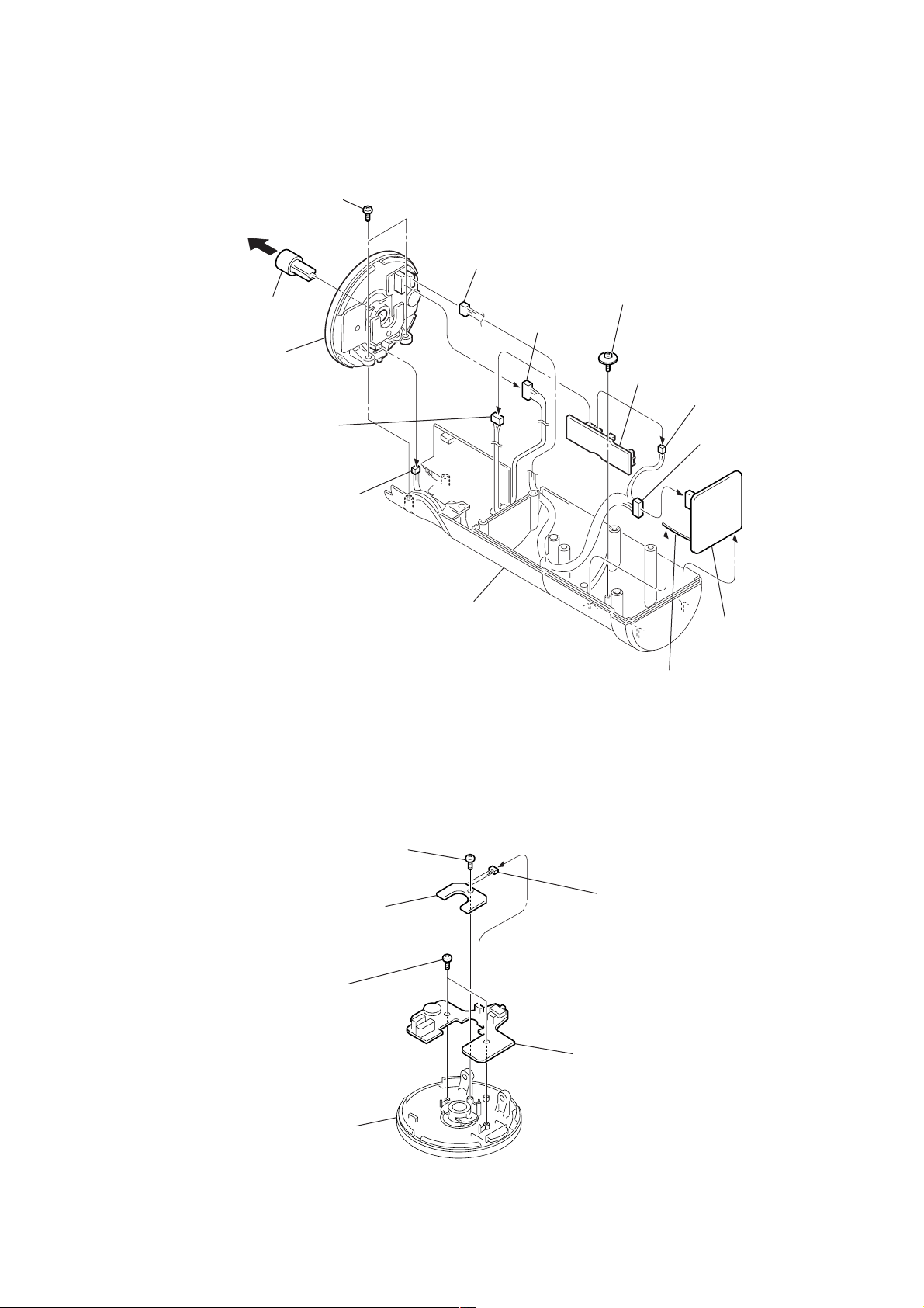
2-4. Cabinet (Top Section), JACK board, RX board
d
)
5
(+BVTP 3
3
power button
6
cabinet
(top section)
7
connector (CN801)
two screws
×
10)
1
connector (CN302)
2
connector
(CN301)
SRS-RF90R/RF90RK/TMR-RF90
9
screw (DIA. 12)
q;
JACK board
8
connector
(CN804)
qa
connector
(CN101)
4
connector (CN304)
2-5. CHARGE board, SW board
3
CHARGE board
1
screw
(+P 2.6
×
4)
rear cabinet
qs
2
connector (CN303
antenna
qd
RX boar
4
two screws
(+P 2.6
top cover section
×
6)
5
SW board
7
Page 8

SRS-RF90R/RF90RK/TMR-RF90
)
2-6. AMP board, MEGABASS board, REFLECTOR board
7
Remove eight solderings.
8
MEGABASS board
9
connector (CN304)
2
connector (CN202)
1
power button
3
screw
(+P 2.6
×
6)
6
AMP board
q;
screw
(+P 2.6
qa
REFLECTOR board
×
6)
5
connector (CNP201
2-7. Drive (030F034)
1
screw
(+BVTP 3
×
10)
2
screw
(+P 2.6
×
6)
8
screw
(+BVTP 3
9
screw
(+P 2.6
×
×
6)
10)
3
Remove two solderings.
qa
herness
4
6
7
drive (030F034)
5
grille (DIA. 30)
connector (CNP202)
4
herness
MDD holder (R)
qf
drive (030F034)
qd
MDD holder (L)
q;
Remove the soldering.
qs
grille (DIA. 30)
1
When you remove a Cautions : (R) side, please start with
, when you remove the (L) side, please start with 8.
8
Page 9

t
digtal voltmeter
(AC range)
TMR-RF90
SRS-RF90R/RF90RK/TMR-RF90
SECTION 3
ELECTRICAL ADJUSTMENTS
Setting :
AF signal
generator
set
TMR-RF90
L-CH (J402)
Telescopic
antenna
Frequency counter
8 cm
set
TMR-RF90
Transmission Frequency Check and Adjustment
1. Set the NOISE FILTER switch to off.
2. Input a signal of 1 kHz 40 mVrms to only the L-CH (J402).
3. Connect a telescopic antenna to the frequency counter input and
extend the antenna to a length of approximately 8 cm.
4. Place TX board close to the frequency counter, then measure the
frequencies of CH1, CH2 and CH3 and make sure the values are
as follows:
CH1 : 913.5 MHz ± 200 kHz
CH2 : 914.0 MHz ± 200 kHz
CH3 : 914.5 MHz ± 200 kHz
Modulation Check and Adjustment
1. Set the channel to CH2.
2. An electric wave is output for 5or 10 minutes when off to on a
power supply (Power indicator will on).
3. Measure the center terminal of RV403 using an digital volt-meter
(AC range) and make sure the value is 2 to 2.5mVrms.
If the measured value is other than the specified value, adjust to
2 to 2.5mVrms by turning the RV403 on the TX board.
Connection points and Adjustment Location :
TX BOARD
←
CH2 ←CH1
CH3
S402
RV403
(Component side)
(L-CH) (R-CH)
J402
VCO UNIT
Hole
When the frequency is not satisfied the specified value, set the
CHANNEL switch (S402) to CH2, then adjust the value of the
frequency counter to 914.0 MHz by trimmer capacitor in the VCO
unit.
Standard value :913.9MHz to 914.1MHz
When completed with replacement, recheck the
frequencies of CH1, CH2 and CH3.
RV403: Modulation adjustment
TX BOARD
Trimmer : Transmission
frequency adjustmen
(Conductor side)
IC402
9
Page 10

SRS-RF90R/RF90RK/TMR-RF90
SRS-RF90R
Notes:
1. Use transmitter with check and adjustment already completed.
2. On adjusting the speaker section, use the transmitter as a
jig.
Wireless Active Speaker : SRS-RF90R
Transmitter : TMR-RF90
Procedure:
1. Connect an oscillator with attenuator and terminator (600 Ω)
to the transmitter AUDIO IN-A connector (J402).
2. Connect an AC adapter to the transmitter DC IN 9V jack (J404).
3. Short between Q101 corrector and GND on the RX board.
4. Connect an AC adapter to the speaker DC IN 9V jack (J801).
5. Connect lead wires to IC101 pin 4, pin 6, pin 7 and GND on
the RX board.
6. Connect a resistor 33k Ω between IC101 pin 4 and pin 7.
7. Connect lead wires to the speakers’ terminals (L+,L-,R+,R-)
on the AMP board.
Free Run Frequency Check and Adjustment
1. Set the transmitter AUDIO IN-A connector (J402) to no signal.
Note: In this case, operation time is about 5 or 10 minutes.
Perform confirmation for less than 5 minutes.
2. Check the transmitter power indicator D401 (red) lights.
3. Set the transmitter CHANNEL switch to 1.
4. Connect DC 1.2V across TP102 and GND on the RX board.
5. Connect a frequency counter to IC101 pin 4 and GND on the
RX board, then confirm the frequency within 76kHz
± 50Hz
6. When the frequency dose not satisfy the specified value, adjust
the value of the frequency counter to specification by RV101
on the RX board.
Specified values: 76kHz ± 50Hz.
7. Remove a 33 kΩ resister between IC101 pin 4 and pin 7.
Setting :
13. Switch on the transmitter again.
14. Set the transmitter CHANNEL switch to 1.
15. Push the TUNE switch (S301) to receive radio frequency.
16. Check same step 8.
17. Set the transmitter CHANNEL switch to 3.
18. Push the TUNE switch (S301) to receive radio frequency.
19. Check same step 8.
Setting :
regulated power supply
(DC 1.2V) (from step 6 to step 9)
+
TP102
–
oscilloscope
(step 8, step 16, step 19)
IC101 pin6
CH1 CH2
+
–+–
IC101 pin4
Carrier Modulation Check
1. Set the transmitter CHANNEL switch to 2.
2. Set the transmitter NOISE FILTER switch to off.
3. Input a signal of 1kHz, 316mVrms to transmitter AUDIO IN-A
(L-ch) connector only.
4. Set the speaker volume (RV301) to minimum.
5. Connect an oscilloscope CH1 and CH2 to IC101 pin 6 and pin 4.
6. Push the TUNE switch (S301) to receive radio frequency.
7. Check the waveform of the oscilloscope that the CH1 is
demodulated 1kHz signal and CH2 is GND.
8. Connect an AC voltmeter with LPF to IC101 pin 6 and GND.
9. Check the value of the AC voltmeter to 26mVrms ± 2mV
Setting :
digital voltmeter
(AC range)
+
–
LPF
2.2K
33000P
IC101
pin6
IC101
pin6
oscilloscope
CH1 CH2
+
–+–
IC101
pin4
regulated power supply
(DC 1.2V)
TP102
+
–
frequency counter
+
IC101 pin4
–
Receiving Frequency Check and Adjustment
1. Set the transmitter CHANNEL switch to 2.
2. Set the transmitter NOISE FILTER switch to off.
3. Input a signal of 1kHz, 316mVrms to transmitter AUDIO INA(L-ch) connector only.
4. Keep distance between transmitter and speaker to 5 meters over.
5. Set the speaker volume (RV301) to minimum.
6. Connect DC1.2V across TP102 and GND.
7. Connect an oscilloscope CH1 and CH2 to IC101 pin 6 and pin 4.
8. Check the waveform of the oscilloscope to CH1 is demodulated
1kHz signal and CH2 is GND.
9. If CH1 and CH2 are not satisfied in step 8, adjust the coil (L101)
on the RX board to satisfied step 8.
10. Disconnect DC1.2V across TP102 and GND.
11. Open between Q101 corrector and GND on the RX board.
12. Switch the transmitter off and push the TUNE switch (S301).
Check the waveform of the oscilloscope at the TP102 as follows:
Setting :
oscilloscope
Waveform of
auto-tuning
voltage at
the TP102
1.8V
GND
2-3sec
0.6V
TP102
CH1
+
–
Separation Check
1. Set the transmitter CHANNEL switch to 2.
2. Set the transmitter NOISE FILTER switch to off.
3. Input a signal of 1kHz, 316mVrms to transmitter AUDIO IN-A
(L-ch) connector only.
4. Connect an oscilloscope CH1 to speakers terminal (L+,L-) and
CH2 to IC101 pin 4 and GND.
5. Push the TUNE switch (S301) to receive radio frequency.
6. Check the waveform of the oscilloscope that the CH1 is
demodulated 1kHz signal and CH2 is GND.
7. Connect an AC voltmeter with LPF to speakers terminal
(L+,L-).
8. Adjust the value of the AC voltmeter to specification by
speaker volume RV301.
Specified values: 155mVrms
9. Connect an AC voltmeter with LPF to speakers terminal
(R+,R-).
10. Measure the value of the AC voltmeter.
11. Check the difference of the L and R to more than 20dB.
12. Input a signal of 1kHz, 316mVrms to transmitter AUDIO IN-A
(R-ch) connector only.
13. Connect an AC voltmeter with LPF to speakers terminal
(R+,R-).
14. Adjust the value of the AC voltmeter to specification by
speaker volume RV301.
Specified values: 155mVrms
15. Connect an AC voltmeter with LPF to speakers terminal
(L+,L-).
16. Measure the value of the AC voltmeter.
10
Page 11

4
17. Check the difference of the L and R to more than 20 dB.
y
digital voltmeter
(AC range)
oscilloscope
SRS-RF90R/RF90RK/TMR-RF90
L+ / R+
+
L– / R–
–
Asjustment Location :
RX BOARD
(Conductor side)
L+
L–
CH1 CH2
+
–+–
IC101
IC101 pin
7
IC101
4
(Connect a 33 KΩ resistor)
IC101
6
RV101:
Free Run Frequenc
Adjustment
TP102
GND
Q101 collector
L101:
Receiving Frequency
Adjustment
11
Page 12

SRS-RF90R/RF90RK/TMR-RF90
Note on Printed Wiring Boards:
• X : parts extracted from the component side.
• b : Pattern from the side which enables seeing.
Note on Schematic Diagram:
• All capacitors are in µF unless otherwise noted. pF: µµF
50 WV or less are not indicated except for electrolytics
and tantalums.
• All resistors are in Ω and 1/
specified.
• C : panel designation.
• A : B+ Line.
• H : adjustment for repair.
• Power voltage is dc 9V and fed with regulated dc power
supply from battery terminal.
• Voltages is dc with respect to ground under no-signal
(detuned) conditions.
• Voltages are taken with a VOM (Input impedance 10 MΩ).
Voltage variations may be noted due to normal production tolerances.
• Signal path.
K
: FM
L : AUDIO
SECTION 4
DIAGRAMS
4
W or less unless otherwise
• CIRCUIT BOARDS LOCATION (SRS-RF90R)
CHARGE board
AMP board
RX board
SW board
REFLECTOR board
MEGABASS board
JACK board
12
Page 13

4-1. Block Diagrams
(SRS-RF90R)
(ANT)
FRONT END
FE UNIT
(914MHz)
L101
TRANSMISSION
FREQUENCY
D101
SRS-RF90R/RF90RK/TMR-RF90
+V
L102
20
FM IF/
CF102
10.7MHz
CF101
10.7MHz
REG
21
+V
IC102
COUNTER
B6
B5
B4
B3
B2
B1
B0
CLK
1316
DISCRI
26
AUTO
BLEND
MUTE
Q102
OSC
Q101
SWITCH
18
FM FE
22
+V
L101
FM
OSC
(DAC)
+2.2V
R
3
4
5
6 1
9
11
12
64R
IC101
IF AMP/DECODE
PD1
PD1
FREE RUN
FREQUENCY
1/2
COUNTER
VCO
27
RV101
DECODE
AMP
MONO/ST
SW
DETUNE
MUTE
STEREO
IND
TUNING
IND
+2.4V
31
Q105
MUTING
R-CH
OFF ON
IC201
AMP
S201
POWER
R-CH
7
10 15
R-CH
Q901
HPF
TWIN-T
FILTER
10
Q202,
D201, 202
LIMITER
IC202
POWER AMP
IC203
POWER AMP
2
2
15
J801
DC IN 9V
R-CH
R-CH
SP1
(SPEAKER)
SP2
(SPEAKER)
SP3
(WOOFER)
RV301
2
VOL
6
5
10
12
Q104
+2.4V
REG
R-CH
Q103
+2.2V
Q107
BUFFER
6
5
CK
1
D
2
S301
TUNE
POWER AMP B+
IC105
+5V
1 3
REG
IC103
COMP.
72
IC104
D-FF
CLR
6
1
3
3
Q
5
Q
• Signal path.
: FM
: AUDIO
• R-ch is omitted due to same as L-ch.
IC201, Q901
D601
POWER
D701
(REFLECTOR)
Q204
RIPPLE
FILTER
Q203
LED
DRIVER
S302
LIGHT
D204
D203
OFFON
D602
CHARGE
RECHARGEABLE BATTERY
(NICKEL-CADMIUM)
6PCS, 7.2V
1313
Page 14

SRS-RF90R/RF90RK/TMR-RF90
(TMR-RF90)
B
AUDIO IN
A
J401
L
R R-CH
R-CH
J402
• R-ch is omitted due to same as L-ch.
• Signal path.
L : AUDIO
F : FM
S401
NOISE FILTER
OFF
ON
NOISE
FILTER
IC401
ALC
13 1
AMP
R-CH
IC403
STEREO MPX
LPF
R-CH
CH2
14 9
AMP
CH1
1
AMP
TIME
DIVISION
MPX
BUFFER
OSC
AMP
X401
38kHz
RV403
MODULATION
BUFFER
DIVIDER
76
8
B+
5V
(STEREO COMPOSITE SIGNAL)
Q408
CHANNEL
SET
Q401
BUFFER
D404,405
RECT
1
2
3
S402
CHANNEL
Q402,405
INPUT
DET
I
MOD IN
(VCO UNIT)
ANT
B+
5V
5V
ANT401
1 3
IC402
+5V
REG
D401
POWER
Q404
B+
SWITCH
Q406
POWER
ON/OFF
J404
DC IN 9V
1414
Page 15

4-2. Printed Wiring Boards (SRS-RF90R) – RX Board Section –
SRS-RF90R/RF90RK/TMR-RF90
A
B
C
12
IC105
TO
17
345678910
TO
17
IC104
IC103
IC101
D
E
F
FE UNIT
IC102
• Semiconductor
Location
Ref. No. Location
D101 D-3
D102 D-2
D103 B-4
D601 F-6
D602 F-6
D701 F-9
IC101 C-3
IC102 D-3
IC103 C-4
IC104 C-3
IC105 B-3
Q101 B-4
Q102 B-4
Q103 C-4
Q104 B-3
Q105 C-2
Q106 C-2
Q107 C-2
1515
Page 16

SRS-RF90R/RF90RK/TMR-RF90
4-3. Schematic Diagram (SRS-RF90R) – RX Board Section –
• IC Block Diagram
IC104 TC7W74FU
Vcc PR CLR Q
8 7 6 5
S
DQ
Q
C
R
1 2 3 4
CK D Q GND
1616
Page 17

4-4. Printed Wiring Boards (SRS-RF90R) – AMP Board Section –
SRS-RF90R/RF90RK/TMR-RF90
A
B
C
12
3456789
• Semiconductor
Location
Ref. No. Location
D201 B-4
D202 B-4
D203 D-5
D204 C-6
D801 E-1
IC201 D-7
IC202 B-6
IC203 B-5
Q202 C-4
Q203 C-4
Q204 D-6
Q901 E-8
IC203
IC202
D
E
F
IC201
TO
RECHARGEABLE
BATTERY
(NICKEL-CADMIUM)
6PCS. 7.2V
TO
1717
Page 18

SRS-RF90R/RF90RK/TMR-RF90
4-5. Schematic Diagram (SRS-RF90R) – AMP Board Section –
• IC Block Diagram
IC202, 203 TEA2025B
THERMAL
PROTECT
START
CIRCUIT
11
DECOUPLING
14131211109 15 16
22
12345678
1818
Page 19

4-6. Printed Wiring Board (TMR-RF90R)
SRS-RF90R/RF90RK/TMR-RF90
A
B
12
3456
IC402
C
D
E
IC401
VCO UNIT
• Semiconductor
Location
Ref. No. Location
D401 E-3
D403 B-4
D404 E-2
D405 E-2
D406 E-3
D408 E-5
D409 D-4
D410 E-4
IC403
IC401 C-2
IC402 C-5
IC403 E-4
Q401 E-1
Q402 E-3
Q404 C-5
Q405 D-3
Q406 E-3
Q408 C-5
F
1919
Page 20

SRS-RF90R/RF90RK/TMR-RF90
4-7. Schematic Diagram (TMR-RF90)
D401
POWER
• Waveforms
1
IC403 6 TO CRYSTAL
10 µs
52.6
20 µs
/DIV
0.58 Vp-p
µ
s
/DIV
1.8 Vp-p
26.3 µs
500mV/DIV,
2
IC403 8 PILOT OUTPUT
200mV/DIV,
2020
Page 21

NOTE:
• -XX, -X mean standardized parts, so they may
have some differences from the original one.
• Items marked “*” are not stocked since they
are seldom required for routine service. Some
delay should be anticipated when ordering these
items.
• The mechanical parts with no reference number
• Hardware (# mark) list and accessories and
5-1. Front Cabinet Section (SRS-RF90R)
SRS-RF90R/RF90RK/TMR-RF90
SECTION 5
EXPLODED VIEWS
in the exploded views are not supplied.
packing materials are given in the last of this
parts list.
8
• Abbreviation
CND : Canadian model
9
7
6
#2
#1
4
1
2
#2
SP3
#3
#3
10
Rear Cabinet section
5
#1
3
Ref. No. Part No. Description Remarks Ref. No. Part No. Description Remarks
1 3-235-615-01 BRACKET, GRILLE
2 3-235-609-01 STAND
3 3-235-612-01 GRILLE (DIA. 57)
4 X-3381-186-1 CABINET SUB ASSY, FRONT
5 3-232-664-01 FOOT, RUBBER
6 1-756-252-31 BATTERY, NICKEL.CADMIUM
* 7 1-683-318-11 RETAINER BOARD
8 3-235-598-01 REFLECTOR
9 3-235-610-01 HOLDER, REFLECTOR
10 3-235-622-11 HOLDER, JACK
SP3 1-544-997-11 SPEAKER (057F022)
#1 7-685-147-14 SCREW +P 3X10 TYPE2 NON-SLIT
#2 7-685-647-79 SCREW +BVTP 3X10 TYPE2 SLIT
#3 7-685-648-79 SCREW +BVTP 3X12 TYPE2 SLIT
21
Page 22

SRS-RF90R/RF90RK/TMR-RF90
5-2. Rear Cabinet Section (SRS-RF90R)
#4
71
54
#2
63
61
59
64
#4
#5
65
60
#4
#2
58
62
#4
55
66
SP1
SP2
#4
#4
68
67
68
67
69
56
not
supplied
52
51
#2
#4
53
55
not
supplied
75
73
57
72
70
74
Ref. No. Part No. Description Remarks Ref. No. Part No. Description Remarks
51 1-683-315-11 JACK BOARD
52 4-227-899-01 SCREW (DIA. 12), FROATING
53 3-235-597-01 HOLDER (R), MDD
* 54 A-3178-298-A MEGABASS BOARD, COMPLETE
55 3-235-613-01 GRILLE (DIA. 30)
56 A-3178-137-A AMP BOARD, COMPLETE
* 57 3-233-819-01 BRACKET (PWB)
58 3-235-596-01 HOLDER (L), MDD
59 1-683-316-11 CHARGE BOARD
60 3-235-601-01 KNOB, VOL
66 1-683-317-11 REFLECTOR BOARD
67 3-235-605-01 PILLAR
68 3-235-617-01 CUSHION, LED
69 3-235-595-11 CABINET, REAR
* 70 A-3178-143-A RX BOARD, COMPLETE
71 3-235-606-01 BUTTON, TUNING
72 3-238-666-01 CUSHION, DC IN
* 73 A-3021-942-A FE UNIT
74 3-831-441-99 CUSHION (LCD)
75 3-840-486-12 CUSHION, SPEAKER
61 1-683-313-11 SW BOARD
62 3-235-600-01 COVER, SWITCH
63 3-235-602-01 LIGHT (CHARGE), GUIDE
64 X-3381-951-1 COVER SUB ASSY, TOP
65 3-235-607-01 BUTTON, POWER
22
SP1 1-542-432-11 DRIVE (030F034)
SP2 1-542-432-11 DRIVE (030F034)
#2 7-685-647-79 SCREW +BVTP 3X10 TYPE2 SLIT
#4 7-685-133-19 SCREW +P 2.6X6 TYPE2
#5 7-685-131-19 SCREW +P 2.6X4 TYPE2 NON-SLIT
Page 23

5-3. TMR-RF90
SRS-RF90R/RF90RK/TMR-RF90
106
105
107
ANT401
#6
103
101
not
supplied
not
supplied
104
108
102
#6
#7
Ref. No. Part No. Description Remarks Ref. No. Part No. Description Remarks
101 X-3381-187-1 CABINET SUB ASSY, LOWER
102 4-984-729-01 FOOT, RUBBER
* 103 A-3178-145-A TX BOARD, COMPLETE
104 3-235-599-01 LIGHT (POWER), GUIDE,
105 3-241-823-01 SHEET, BLIND
106 3-235-620-01 CABINET (UPPER)(US)
106 3-235-620-11 CABINET (UPPER)(CND)
107 X-3381-189-1 ANTENNA SUB ASSY
* 108 A-3021-940-A VCO UNIT
ANT401 4-213-164-01 TERMINAL, ANTENNA
#6 7-685-103-19 SCREW +P 2X5 TYPE2 NON-SLIT
#7 7-685-105-19 SCREW +P 2X8 TYPE2 NON-SLIT
23
Page 24

SRS-RF90R/RF90RK/TMR-RF90
SECTION 6
AMP
NOTE:
• Due to standardization, replacements in the
parts list may be different from the parts
specified in the diagrams or the components
used on the set.
• -XX, -X mean standardized parts, so they
may have some difference from the original
one.
• Items marked “*” are not stocked since they
are seldom required for routine service.
Some delay should be anticipated when
ordering these items.
Ref. No. Part No. Description Remarks Ref. No. Part No. Description Remarks
* A-3178-137-A AMP BOARD, COMPLETE
(including MEGABASS BOARD, COMPLETE)
**************************************
< CAPACITOR >
ELECTRICAL PARTS LIST
• CAPACITORS:
uF: µF
• RESISTORS
All resistors are in ohms.
METAL: metal-film resistor
METAL OXIDE: Metal Oxide-film resistor
F: nonflammable
• COILS
uH: µH
When indicating parts by reference number,
please include the board name.
C254 1-126-933-11 ELECT 100uF 20.00% 16V
C255 1-126-933-11 ELECT 100uF 20.00% 16V
C256 1-130-497-00 MYLAR 0.15uF 5% 50V
C257 1-162-964-11 CERAMIC CHIP 0.001uF 10% 50V
C259 1-126-933-11 ELECT 100uF 20.00% 16V
• SEMICONDUCTORS
In each case, u: µ, for example:
uA...: µA... , uPA... , µPA... ,
uPB... , µPB... , uPC... , µPC... ,
uPD..., µPD...
The components identified by mark 0 or
dotted line with mark 0 are critical for safety.
Replace only with part number specified.
Les composants identifiés par une marque
0 sont critiques pour la sécurité.
Ne les remplacer que par une pièce portant
le numéro spécifié.
C201 1-162-962-11 CERAMIC CHIP 470PF 10% 50V
C202 1-162-962-11 CERAMIC CHIP 470PF 10% 50V
C203 1-126-160-11 ELECT 1uF 20% 50V
C204 1-126-160-11 ELECT 1uF 20% 50V
C205 1-162-927-11 CERAMIC CHIP 100PF 5% 50V
C206 1-162-927-11 CERAMIC CHIP 100PF 5% 50V
C207 1-124-233-11 ELECT 10uF 20.00% 16V
C208 1-115-412-11 CERAMIC CHIP 680PF 5.00% 25V
C209 1-124-233-11 ELECT 10uF 20.00% 16V
C210 1-115-412-11 CERAMIC CHIP 680PF 5.00% 25V
C211 1-162-974-11 CERAMIC CHIP 0.01uF 50V
C212 1-126-382-11 ELECT 100uF 20.00% 16V
C213 1-162-974-11 CERAMIC CHIP 0.01uF 50V
C214 1-124-259-11 ELECT 4.7uF 20.00% 16V
C215 1-124-259-11 ELECT 4.7uF 20.00% 16V
C216 1-124-259-11 ELECT 4.7uF 20.00% 16V
C217 1-126-160-11 ELECT 1uF 20% 50V
C218 1-126-160-11 ELECT 1uF 20% 50V
C219 1-162-927-11 CERAMIC CHIP 100PF 5% 50V
C221 1-126-933-11 ELECT 100uF 20.00% 16V
C222 1-126-160-11 ELECT 1uF 20% 50V
C223 1-126-933-11 ELECT 100uF 20.00% 16V
C224 1-130-497-00 MYLAR 0.15uF 5% 50V
C225 1-126-786-11 ELECT 47uF 20.00% 16V
C226 1-162-927-11 CERAMIC CHIP 100PF 5% 50V
C229 1-126-160-11 ELECT 1uF 20% 50V
C230 1-126-933-11 ELECT 100uF 20.00% 16V
C231 1-130-497-00 MYLAR 0.15uF 5% 50V
C232 1-162-974-11 CERAMIC CHIP 0.01uF 50V
C233 1-126-933-11 ELECT 100uF 20.00% 16V
C234 1-126-786-11 ELECT 47uF 20.00% 16V
C235 1-126-786-11 ELECT 47uF 20.00% 16V
C237 1-162-921-11 CERAMIC CHIP 33PF 5% 50V
C238 1-162-921-11 CERAMIC CHIP 33PF 5% 50V
C240 1-126-382-11 ELECT 100uF 20.00% 16V
C241 1-124-233-11 ELECT 10uF 20.00% 16V
C242 1-162-968-11 CERAMIC CHIP 0.0047uF 10% 50V
C243 1-162-968-11 CERAMIC CHIP 0.0047uF 10% 50V
C244 1-162-968-11 CERAMIC CHIP 0.0047uF 10% 50V
C245 1-162-968-11 CERAMIC CHIP 0.0047uF 10% 50V
C246 1-126-160-11 ELECT 1uF 20% 50V
C247 1-124-233-11 ELECT 10uF 20.00% 16V
C250 1-124-233-11 ELECT 10uF 20.00% 16V
C251 1-119-866-11 CERAMIC CHIP 0.68uF 10.00% 10V
C253 1-126-933-11 ELECT 100uF 20.00% 16V
C260 1-126-933-11 ELECT 100uF 20.00% 16V
C261 1-130-497-00 MYLAR 0.15uF 5% 50V
C262 1-162-974-11 CERAMIC CHIP 0.01uF 50V
C263 1-126-933-11 ELECT 100uF 20.00% 16V
C269 1-126-943-11 ELECT 2200uF 20.00% 25V
C270 1-126-382-11 ELECT 100uF 20.00% 16V
< CONNECTOR >
* CN202 1-506-986-11 PIN, CONNECTOR (PC BOARD) 4P
* CN203 1-506-984-11 PIN, CONNECTOR (PC BOARD) 2P
< DIODE >
D201 8-719-988-61 DIODE 1SS355TE-17
D202 8-719-988-61 DIODE 1SS355TE-17
D203 8-719-422-31 DIODE MA8047-M-TX
D204 8-719-988-61 DIODE 1SS355TE-17
< CONDUCTOR >
FB202 1-216-864-11 METAL CHIP 0 5% 1/16W
FB203 1-216-864-11 METAL CHIP 0 5% 1/16W
FB204 1-216-864-11 METAL CHIP 0 5% 1/16W
< IC >
IC201 8-759-100-96 IC NJM4558M-TE2
IC202 8-759-512-88 IC TEA2025B
IC203 8-759-512-88 IC TEA2025B
< CONDUCTOR >
JC202 1-216-864-11 METAL CHIP 0 5% 1/16W
JC203 1-216-864-11 METAL CHIP 0 5% 1/16W
< TRANSISTOR >
Q202 8-729-200-72 TRANSISTOR 2SC2712L-TE85L
Q203 8-729-200-72 TRANSISTOR 2SC2712L-TE85L
Q204 8-729-200-72 TRANSISTOR 2SC2712L-TE85L
< RESISTOR >
R201 1-216-833-11 METAL CHIP 10K 5% 1/16W
R202 1-216-833-11 METAL CHIP 10K 5% 1/16W
R203 1-216-837-11 METAL CHIP 22K 5% 1/16W
R204 1-216-837-11 METAL CHIP 22K 5% 1/16W
R205 1-216-821-11 METAL CHIP 1K 5% 1/16W
24
Page 25

SRS-RF90R/RF90RK/TMR-RF90
AMP
CHARGE JACK
MEGABASS REFLECTOR RX
Ref. No. Part No. Description Remarks Ref. No. Part No. Description Remarks
R206 1-216-833-11 METAL CHIP 10K 5% 1/16W
R207 1-216-833-11 METAL CHIP 10K 5% 1/16W
R208 1-216-821-11 METAL CHIP 1K 5% 1/16W
R209 1-216-829-11 METAL CHIP 4.7K 5% 1/16W
R210 1-216-830-11 METAL CHIP 5.6K 5% 1/16W
R211 1-216-821-11 METAL CHIP 1K 5% 1/16W
R212 1-216-833-11 METAL CHIP 10K 5% 1/16W
R213 1-216-833-11 METAL CHIP 10K 5% 1/16W
R214 1-216-833-11 METAL CHIP 10K 5% 1/16W
R218 1-216-808-11 METAL CHIP 82 5% 1/16W
R219 1-216-808-11 METAL CHIP 82 5% 1/16W
R224 1-216-809-11 METAL CHIP 100 5% 1/16W
R225 1-218-272-11 RES-CHIP 5.1K 5% 1/10W
R226 1-218-272-11 RES-CHIP 5.1K 5% 1/10W
R227 1-218-272-11 RES-CHIP 5.1K 5% 1/10W
J801 1-785-066-11 JACK,DC(POLARITY UNIFIED TYPE) (DC IN 9V)
************************************************************
* A-3178-298-A MEGABASS BOARD, COMPLETE
C901 1-125-837-11 CERAMIC CHIP 1uF 10% 6.3V
C902 1-125-837-11 CERAMIC CHIP 1uF 10% 6.3V
C903 1-162-927-11 CERAMIC CHIP 100PF 5% 50V
C904 1-162-962-11 CERAMIC CHIP 470PF 10% 50V
C905 1-162-974-11 CERAMIC CHIP 0.01uF 50V
< JACK >
**************************
< CAPACITOR >
< CONNECTOR >
R228 1-218-272-11 RES-CHIP 5.1K 5% 1/10W
R229 1-216-822-11 METAL CHIP 1.2K 5% 1/16W
R230 1-216-829-11 METAL CHIP 4.7K 5% 1/16W
R231 1-216-841-11 METAL CHIP 47K 5% 1/16W
R232 1-216-833-11 METAL CHIP 10K 5% 1/16W
R233 1-216-833-11 METAL CHIP 10K 5% 1/16W
R234 1-216-826-11 METAL CHIP 2.7K 5% 1/16W
R235 1-216-833-11 METAL CHIP 10K 5% 1/16W
R236 1-216-817-11 METAL CHIP 470 5% 1/16W
R237 1-216-821-11 METAL CHIP 1K 5% 1/16W
R238 1-216-808-11 METAL CHIP 82 5% 1/16W
R240 1-216-042-00 METAL CHIP 510 5% 1/10W
R241 1-216-042-00 METAL CHIP 510 5% 1/10W
R242 1-216-042-00 METAL CHIP 510 5% 1/10W
R243 1-216-042-00 METAL CHIP 510 5% 1/10W
R246 1-216-833-11 METAL CHIP 10K 5% 1/16W
R247 1-216-808-11 METAL CHIP 82 5% 1/16W
< SWITCH >
S201 1-786-285-11 SWITCH, PUSH (2 KEY)(POWER, CHARGE)
************************************************************
* 1-683-316-11 CHARGE BOARD
**************
< DIODE >
CNP901 1-794-496-11 PIN, CONNECTOR 5P
CNP902 1-815-398-11 PIN, CONNECTOR 3P
< CONDUCTOR >
FB901 1-216-864-11 METAL CHIP 0 5% 1/16W
< TRANSISTOR >
Q901 8-729-200-72 TRANSISTOR 2SC2712L-TE85L
< RESISTOR >
R901 1-216-833-11 METAL CHIP 10K 5% 1/16W
R902 1-216-833-11 METAL CHIP 10K 5% 1/16W
R903 1-216-826-11 METAL CHIP 2.7K 5% 1/16W
R904 1-216-833-11 METAL CHIP 10K 5% 1/16W
R905 1-216-833-11 METAL CHIP 10K 5% 1/16W
R906 1-216-826-11 METAL CHIP 2.7K 5% 1/16W
R907 1-216-826-11 METAL CHIP 2.7K 5% 1/16W
R908 1-218-917-11 RES-CHIP 820K 5% 1/10W
R909 1-216-817-11 METAL CHIP 470 5% 1/16W
R910 1-218-917-11 RES-CHIP 820K 5% 1/10W
R911 1-216-822-11 METAL CHIP 1.2K 5% 1/16W
************************************************************
* 1-683-317-11 REFLECTOR BOARD
*****************
D601 8-719-059-98 DIODE SLR-342VCTB7(POWER)
D602 8-719-072-97 DIODE TLG124A(TPJ52)(CHARGE)
************************************************************
* 1-683-315-11 JACK BOARD
***********
< CAPACITOR >
C802 1-163-021-11 CERAMIC CHIP 0.01uF 10.00% 50V
C803 1-163-021-11 CERAMIC CHIP 0.01uF 10.00% 50V
< CONNECTOR >
* CN801 1-566-002-11 PIN, CONNECTOR (PC BOARD) 5P
* CN802 1-568-482-11 PIN, CONNECTOR (PC BOARD) 2P
* CN804 1-506-998-11 PIN, CONNECTOR (PC BOARD) 2P
< DIODE >
D801 8-719-210-33 DIODE EC10DS2TE12L
< CAPACITOR >
C701 1-164-156-11 CERAMIC CHIP 0.1uF 25V
< DIODE >
D701 6-500-200-01 DIODE HLMP-NS30-S0000(REFLECTOR)
************************************************************
* A-3178-143-A RX BOARD, COMPLETE
*******************
* A-3021-942-A FE UNIT
< CAPACITOR >
C101 1-124-233-11 ELECT 10uF 20.00% 16V
C103 1-126-162-11 ELECT 3.3uF 20% 50V
C104 1-164-156-11 CERAMIC CHIP 0.1uF 25V
C105 1-124-233-11 ELECT 10uF 20.00% 16V
C106 1-162-970-11 CERAMIC CHIP 0.01uF 10% 25V
25
Page 26

SRS-RF90R/RF90RK/TMR-RF90
RX
Ref. No. Part No. Description Remarks Ref. No. Part No. Description Remarks
C107 1-162-921-11 CERAMIC CHIP 33PF 5% 50V
C108 1-162-908-11 CERAMIC CHIP 3PF 8.33% 50V
C109 1-162-924-11 CERAMIC CHIP 56PF 5.00% 50V
C110 1-162-924-11 CERAMIC CHIP 56PF 5.00% 50V
C111 1-162-970-11 CERAMIC CHIP 0.01uF 10% 25V
C112 1-124-259-11 ELECT 4.7uF 20.00% 16V
C113 1-113-619-11 CERAMIC CHIP 0.47uF 10V
C114 1-115-156-11 CERAMIC CHIP 1uF 10V
C115 1-164-227-11 CERAMIC CHIP 0.022uF 10% 25V
C116 1-164-227-11 CERAMIC CHIP 0.022uF 10% 25V
C117 1-124-234-00 ELECT 22uF 20% 16V
C118 1-162-970-11 CERAMIC CHIP 0.01uF 10% 25V
C119 1-124-234-00 ELECT 22uF 20% 16V
C120 1-104-942-11 ELECT 1uF 20.00% 50V
C121 1-104-942-11 ELECT 1uF 20.00% 50V
C122 1-115-156-11 CERAMIC CHIP 1uF 10V
C123 1-162-970-11 CERAMIC CHIP 0.01uF 10% 25V
C124 1-162-970-11 CERAMIC CHIP 0.01uF 10% 25V
C125 1-126-786-11 ELECT 47uF 20.00% 16V
C126 1-164-156-11 CERAMIC CHIP 0.1uF 25V
C127 1-164-156-11 CERAMIC CHIP 0.1uF 25V
C128 1-164-230-11 CERAMIC CHIP 220PF 5.00% 50V
C129 1-162-970-11 CERAMIC CHIP 0.01uF 10% 25V
C130 1-162-970-11 CERAMIC CHIP 0.01uF 10% 25V
C131 1-164-156-11 CERAMIC CHIP 0.1uF 25V
C132 1-164-156-11 CERAMIC CHIP 0.1uF 25V
C133 1-126-786-11 ELECT 47uF 20.00% 16V
C134 1-164-156-11 CERAMIC CHIP 0.1uF 25V
C135 1-162-964-11 CERAMIC CHIP 0.001uF 10% 50V
C136 1-164-156-11 CERAMIC CHIP 0.1uF 25V
C137 1-124-233-11 ELECT 10uF 20.00% 16V
C138 1-164-156-11 CERAMIC CHIP 0.1uF 25V
C139 1-104-942-11 ELECT 1uF 20.00% 50V
C140 1-104-942-11 ELECT 1uF 20.00% 50V
C141 1-162-970-11 CERAMIC CHIP 0.01uF 10% 25V
C142 1-162-920-11 CERAMIC CHIP 27PF 5% 50V
C143 1-115-156-11 CERAMIC CHIP 1uF 10V
C146 1-162-927-11 CERAMIC CHIP 100PF 5% 50V
C147 1-162-964-11 CERAMIC CHIP 0.001uF 10% 50V
C149 1-164-156-11 CERAMIC CHIP 0.1uF 25V
C150 1-162-970-11 CERAMIC CHIP 0.01uF 10% 25V
C151 1-164-156-11 CERAMIC CHIP 0.1uF 25V
IC101 8-752-072-12 IC CXA1538N-T4
IC102 8-759-453-43 IC TC74HC4024AF(EL)
IC103 8-759-510-73 IC BA10393F-E2
IC104 8-759-083-94 IC TC7W74FU(TE12R)
IC105 8-759-537-90 IC KIA78S05P-TP
JC103 1-216-864-11 METAL CHIP 0 5% 1/16W
JC104 1-216-864-11 METAL CHIP 0 5% 1/16W
JC105 1-216-864-11 METAL CHIP 0 5% 1/16W
JC106 1-216-864-11 METAL CHIP 0 5% 1/16W
JC107 1-216-864-11 METAL CHIP 0 5% 1/16W
JC108 1-216-864-11 METAL CHIP 0 5% 1/16W
JC110 1-216-864-11 METAL CHIP 0 5% 1/16W
JC111 1-216-864-11 METAL CHIP 0 5% 1/16W
JC112 1-216-864-11 METAL CHIP 0 5% 1/16W
L101 1-428-911-11 COIL, AIR-CORE
L102 1-412-933-11 INDUCTOR 0.33uH
Q101 8-729-200-72 TRANSISTOR 2SC2712L-TE85L
Q102 8-729-903-10 TRANSISTOR FMW1-T-148
Q103 8-729-027-44 TRANSISTOR DTC114TKA-T146
Q104 8-729-212-02 TRANSISTOR KTC3203Y-AT
Q105 8-729-043-69 TRANSISTOR UN2225-(TX).S0
Q106 8-729-043-69 TRANSISTOR UN2225-(TX).S0
Q107 8-729-200-72 TRANSISTOR 2SC2712L-TE85L
R101 1-216-827-11 METAL CHIP 3.3K 5% 1/16W
R102 1-216-835-11 METAL CHIP 15K 5% 1/16W
R103 1-216-845-11 METAL CHIP 100K 5% 1/16W
R104 1-216-825-11 METAL CHIP 2.2K 5% 1/16W
R105 1-216-797-11 METAL CHIP 10 5% 1/16W
R106 1-216-825-11 METAL CHIP 2.2K 5% 1/16W
R107 1-216-827-11 METAL CHIP 3.3K 5% 1/16W
R108 1-216-827-11 METAL CHIP 3.3K 5% 1/16W
R109 1-216-797-11 METAL CHIP 10 5% 1/16W
R111 1-216-825-11 METAL CHIP 2.2K 5% 1/16W
< IC >
< CONDUCTOR >
< COIL >
< TRANSISTOR >
< RESISTOR >
< FILTER >
CF101 1-577-572-11 FILTER, CERAMIC
CF102 1-577-588-11 FILTER, CERAMIC
< CONNECTOR >
* CN101 1-564-779-11 PLUG, CONNECTOR (2.5MM) 6P
< DIODE >
D101 8-719-083-90 DIODE HVU363ATRU
D102 8-719-063-66 DIODE RD2.2SB-T1
D103 8-719-056-74 DIODE UDZ-TE-17-3.0B
26
R112 1-216-811-11 METAL CHIP 150 5% 1/16W
R113 1-216-815-11 METAL CHIP 330 5% 1/16W
R114 1-216-811-11 METAL CHIP 150 5% 1/16W
R115 1-218-867-11 RES-CHIP 6.8K 5% 1/10W
R116 1-216-853-11 METAL CHIP 470K 5% 1/16W
R117 1-218-749-11 RES-CHIP 240K 5% 1/10W
R118 1-216-846-11 METAL CHIP 120K 5% 1/16W
R119 1-216-833-11 METAL CHIP 10K 5% 1/16W
R120 1-218-344-11 RES-CHIP 7.5K 5% 1/10W
R121 1-216-835-11 METAL CHIP 15K 5% 1/16W
R122 1-218-727-11 RES-CHIP 30K 5% 1/10W
R123 1-218-890-11 RES-CHIP 62K 5% 1/10W
R124 1-216-841-11 METAL CHIP 47K 5% 1/16W
R125 1-216-857-11 METAL CHIP 1M 5% 1/16W
R126 1-216-835-11 METAL CHIP 15K 5% 1/16W
Page 27

SRS-RF90R/RF90RK/TMR-RF90
RX TXSW
Ref. No. Part No. Description Remarks Ref. No. Part No. Description Remarks
R127 1-216-835-11 METAL CHIP 15K 5% 1/16W
R128 1-216-857-11 METAL CHIP 1M 5% 1/16W
R129 1-216-841-11 METAL CHIP 47K 5% 1/16W
R130 1-216-837-11 METAL CHIP 22K 5% 1/16W
R131 1-216-841-11 METAL CHIP 47K 5% 1/16W
* A-3178-145-A TX BOARD, COMPLETE
*******************
* A-3021-940-A VCO UNIT
< CAPACITOR >
R132 1-216-837-11 METAL CHIP 22K 5% 1/16W
R133 1-216-837-11 METAL CHIP 22K 5% 1/16W
R134 1-216-837-11 METAL CHIP 22K 5% 1/16W
R135 1-216-833-11 METAL CHIP 10K 5% 1/16W
R136 1-216-837-11 METAL CHIP 22K 5% 1/16W
R137 1-216-844-11 METAL CHIP 82K 5% 1/16W
R138 1-216-837-11 METAL CHIP 22K 5% 1/16W
R139 1-216-837-11 METAL CHIP 22K 5% 1/16W
R140 1-216-809-11 METAL CHIP 100 5% 1/16W
R141 1-216-816-11 METAL CHIP 390 5% 1/16W
R142 1-216-821-11 METAL CHIP 1K 5% 1/16W
R143 1-216-821-11 METAL CHIP 1K 5% 1/16W
R144 1-216-837-11 METAL CHIP 22K 5% 1/16W
R145 1-216-829-11 METAL CHIP 4.7K 5% 1/16W
R146 1-216-825-11 METAL CHIP 2.2K 5% 1/16W
< VARIABLE RESISTOR >
RV101 1-241-763-11 RES, ADJ, CARBON 4.7K
************************************************************
* 1-683-313-11 SW BOARD
**********
< CONNECTOR >
* CN301 1-506-988-11 PIN, CONNECTOR (PC BOARD) 6P
* CN302 1-506-986-11 PIN, CONNECTOR (PC BOARD) 4P
* CN303 1-506-986-11 PIN, CONNECTOR (PC BOARD) 4P
* CN304 1-506-984-11 PIN, CONNECTOR (PC BOARD) 2P
< FERRITE BEAD >
FB301 1-216-864-11 METAL CHIP 0 5% 1/16W
FB302 1-216-864-11 METAL CHIP 0 5% 1/16W
FB303 1-216-864-11 METAL CHIP 0 5% 1/16W
< RESISTOR >
R301 1-216-817-11 METAL CHIP 470 5% 1/16W
R302 1-216-817-11 METAL CHIP 470 5% 1/16W
R303 1-216-815-11 METAL CHIP 330 5% 1/16W
R306 1-216-821-11 METAL CHIP 1K 5% 1/16W
< VARIABLE RESISTOR >
C403 1-163-009-11 CERAMIC CHIP 0.001uF 10.00% 50V
C406 1-163-037-11 CERAMIC CHIP 0.022uF 10% 25V
C407 1-126-961-11 ELECT 2.2uF 20.00% 50V
C413 1-163-009-11 CERAMIC CHIP 0.001uF 10.00% 50V
C416 1-163-037-11 CERAMIC CHIP 0.022uF 10% 25V
C417 1-126-961-11 ELECT 2.2uF 20.00% 50V
C421 1-124-234-00 ELECT 22uF 20% 16V
C422 1-126-934-11 ELECT 220uF 20.00% 16V
C423 1-163-251-11 CERAMIC CHIP 100PF 5.00% 50V
C425 1-163-037-11 CERAMIC CHIP 0.022uF 10% 25V
C426 1-163-021-11 CERAMIC CHIP 0.01uF 10.00% 50V
C427 1-163-021-11 CERAMIC CHIP 0.01uF 10.00% 50V
C428 1-163-251-11 CERAMIC CHIP 100PF 5.00% 50V
C429 1-163-251-11 CERAMIC CHIP 100PF 5.00% 50V
C430 1-124-259-11 ELECT 4.7uF 20.00% 16V
C431 1-126-157-11 ELECT 10uF 20% 16V
C432 1-163-018-00 CERAMIC CHIP 0.0056uF 5% 50V
C433 1-164-346-11 CERAMIC CHIP 1uF 16V
C436 1-126-157-11 ELECT 10uF 20% 16V
C439 1-135-149-21 TANTALUM CHIP 2.2uF 20% 10V
C440 1-163-251-11 CERAMIC CHIP 100PF 5.00% 50V
C441 1-126-157-11 ELECT 10uF 20% 16V
C442 1-163-018-00 CERAMIC CHIP 0.0056uF 5% 50V
C443 1-164-346-11 CERAMIC CHIP 1uF 16V
C444 1-163-251-11 CERAMIC CHIP 100PF 5.00% 50V
C445 1-163-251-11 CERAMIC CHIP 100PF 5.00% 50V
C451 1-126-934-11 ELECT 220uF 20.00% 16V
C452 1-126-933-11 ELECT 100uF 20.00% 16V
C453 1-126-157-11 ELECT 10uF 20% 16V
C454 1-163-251-11 CERAMIC CHIP 100PF 5.00% 50V
C455 1-163-227-11 CERAMIC CHIP 10PF 5.00% 50V
C457 1-163-003-11 CERAMIC CHIP 330PF 10% 50V
C458 1-126-157-11 ELECT 10uF 20% 16V
C462 1-163-251-11 CERAMIC CHIP 100PF 5.00% 50V
C466 1-163-021-11 CERAMIC CHIP 0.01uF 10.00% 50V
C468 1-163-021-11 CERAMIC CHIP 0.01uF 10.00% 50V
C469 1-163-038-00 CERAMIC CHIP 0.1uF 25V
C470 1-126-786-11 ELECT 47uF 20.00% 16V
C471 1-126-935-11 ELECT 470uF 20.00% 16V
C475 1-163-038-00 CERAMIC CHIP 0.1uF 25V
RV301 1-225-472-11 RES, VAR, CARBON 50K/50K(VOL )
< SWITCH >
S301 1-771-980-11 SWITCH, TACTILE(TUNE)
S302 1-554-574-21 SWITCH, SLIDE(LIGHT)
************************************************************
C478 1-164-182-11 CERAMIC CHIP 0.0033uF 10% 50V
C480 1-163-021-11 CERAMIC CHIP 0.01uF 10.00% 50V
C483 1-163-085-00 CERAMIC CHIP 2PF 50V
< DIODE >
D401 8-719-059-98 DIODE SLR-342VCTB7(POWER)
D403 8-719-200-82 DIODE 11ES2-TA1B
D404 8-719-991-33 DIODE 1SS133T-77
D405 8-719-991-33 DIODE 1SS133T-77
D406 8-719-109-85 DIODE RD5.1ES-T1B2
D408 8-719-109-51 DIODE RD2.0ESB2
D409 8-719-421-40 DIODE MA77-TX
D410 8-719-421-40 DIODE MA77-TX
27
Page 28

SRS-RF90R/RF90RK/TMR-RF90
TX
Ref. No. Part No. Description Remarks Ref. No. Part No. Description Remarks
< IC >
IC401 8-759-998-71 IC BA3308F-E2
IC402 8-759-537-90 IC KIA78S05P-TP
IC403 8-759-667-59 IC NJM2035M(TE2)
R440 1-216-049-11 RES-CHIP 1K 5% 1/10W
R446 1-216-051-00 METAL CHIP 1.2K 5% 1/10W
R448 1-216-049-11 RES-CHIP 1K 5% 1/10W
R449 1-216-081-00 METAL CHIP 22K 5% 1/10W
R452 1-216-081-00 METAL CHIP 22K 5% 1/10W
< JACK >
J401 1-566-822-21 JACK(AUDIO IN)
J402 1-580-441-61 JACK, PIN 2P(AUDIO IN)
J404 1-785-066-11 JACK,DC(POLARITY UNIFIED TYPE)(DC IN 9V)
< CONDUCTOR >
JC404 1-216-295-00 SHORT 0
JC405 1-216-295-00 SHORT 0
JC410 1-216-295-00 SHORT 0
JC430 1-216-295-00 SHORT 0
JC470 1-216-295-00 SHORT 0
< COIL >
L401 1-414-234-11 FERRITE 0uH
L402 1-414-234-11 FERRITE 0uH
L405 1-414-234-11 FERRITE 0uH
L408 1-419-079-21 COIL (MPX FILTER)
L409 1-419-079-21 COIL (MPX FILTER)
L410 1-419-662-11 COIL, AIR-CORE
< TRANSISTOR >
Q401 8-729-200-72 TRANSISTOR 2SC2712L-TE85L
Q402 8-729-200-72 TRANSISTOR 2SC2712L-TE85L
Q404 8-729-045-00 TRANSISTOR KTA1266GR-AT
Q405 8-729-045-00 TRANSISTOR KTA1266GR-AT
Q406 8-729-200-72 TRANSISTOR 2SC2712L-TE85L
R453 1-216-117-00 METAL CHIP 680K 5% 1/10W
R454 1-216-089-00 RES-CHIP 47K 5% 1/10W
R455 1-216-049-11 RES-CHIP 1K 5% 1/10W
R456 1-216-051-00 METAL CHIP 1.2K 5% 1/10W
R457 1-216-065-00 RES-CHIP 4.7K 5% 1/10W
R458 1-216-049-11 RES-CHIP 1K 5% 1/10W
R459 1-216-081-00 METAL CHIP 22K 5% 1/10W
R461 1-216-065-00 RES-CHIP 4.7K 5% 1/10W
R464 1-216-049-11 RES-CHIP 1K 5% 1/10W
R466 1-216-081-00 METAL CHIP 22K 5% 1/10W
R467 1-216-065-00 RES-CHIP 4.7K 5% 1/10W
R469 1-216-103-00 METAL CHIP 180K 5% 1/10W
R472 1-216-041-00 METAL CHIP 470 5% 1/10W
R473 1-216-044-00 METAL CHIP 620 5% 1/10W
R481 1-216-067-00 METAL CHIP 5.6K 5% 1/10W
R482 1-216-081-00 METAL CHIP 22K 5% 1/10W
R483 1-216-057-00 METAL CHIP 2.2K 5% 1/10W
R484 1-216-654-11 METAL CHIP 1.3K 0.5% 1/10W
R485 1-216-051-00 METAL CHIP 1.2K 5% 1/10W
R486 1-216-079-00 METAL CHIP 18K 5% 1/10W
R489 1-216-079-00 METAL CHIP 18K 5% 1/10W
< VARIABLE RESISTOR >
RV403 1-241-763-11 RES, ADJ, CARBON 4.7K
< SWITCH >
Q408 8-729-040-78 TRANSISTOR DTA124GKA-T146
< RESISTOR >
R401 1-216-085-00 RES-CHIP 33K 5% 1/10W
R403 1-216-018-00 METAL CHIP 51 5% 1/10W
R404 1-216-085-00 RES-CHIP 33K 5% 1/10W
R406 1-216-085-00 RES-CHIP 33K 5% 1/10W
R407 1-216-049-11 RES-CHIP 1K 5% 1/10W
R408 1-216-057-00 METAL CHIP 2.2K 5% 1/10W
R411 1-216-085-00 RES-CHIP 33K 5% 1/10W
R413 1-216-018-00 METAL CHIP 51 5% 1/10W
R414 1-216-085-00 RES-CHIP 33K 5% 1/10W
R416 1-216-085-00 RES-CHIP 33K 5% 1/10W
R417 1-216-049-11 RES-CHIP 1K 5% 1/10W
R418 1-216-057-00 METAL CHIP 2.2K 5% 1/10W
R421 1-216-097-11 RES-CHIP 100K 5% 1/10W
R422 1-216-061-00 RES-CHIP 3.3K 5% 1/10W
R423 1-216-033-00 METAL CHIP 220 5% 1/10W
R424 1-216-133-00 RES-CHIP 3.3M 5% 1/10W
R425 1-216-097-11 RES-CHIP 100K 5% 1/10W
R426 1-216-061-00 RES-CHIP 3.3K 5% 1/10W
R427 1-216-033-00 METAL CHIP 220 5% 1/10W
R428 1-216-045-00 METAL CHIP 680 5% 1/10W
R429 1-216-073-00 RES-CHIP 10K 5% 1/10W
R430 1-216-073-00 RES-CHIP 10K 5% 1/10W
R431 1-216-065-00 RES-CHIP 4.7K 5% 1/10W
R433 1-216-081-00 METAL CHIP 22K 5% 1/10W
R438 1-216-105-00 RES-CHIP 220K 5% 1/10W
S401 1-771-961-11 SWITCH, SLIDE(NOISE FILTER)
S402 1-771-962-11 SWITCH, SLIDE(CHANNEL)
< VIBRATOR >
X401 1-781-850-11 VIBRATOR, CRYSTAL(38kHz)
************************************************************
MISCELLANEOUS
***************
6 1-756-252-31 BATTERY, NICKEL.CADMIUM
SP1 1-542-432-11 DRIVE (030F034)
SP2 1-542-432-11 DRIVE (030F034)
SP3 1-544-997-11 SPEAKER (057F022)
************************************************************
ACCESSORIES
************
0 1-473-588-11 ADAPTOR, AC (AC-S901) (FOR TMR-RF90)
0 1-693-029-11 ADAPTOR, A.C. (AC-S906T) (FOR SRS-RF90R)
1-559-906-32 CORD, CONNECTION
3-236-404-11 MANUAL, INSTRUCTION
The components identified by
mark 0 or dotted line with mark
0 are critical for safety.
Replace only with part number
specified.
(ENGLISH, FRENCH, SPANISH)
Les composants identifiés par
une marque 0 sont critiques
pour la sécurité.
Ne les remplacer que par une
pièce portant le numéro spécifié.
28
Page 29

MEMO
SRS-RF90R/RF90RK/TMR-RF90
29
Page 30

SRS-RF90R/RF90RK/TMR-RF90
REVISION HISTORY
Clicking the version allows you to jump to the revised page.
Also, clicking the version at the upper right on the revised page allows you to jump to the next revised
page.
Ver. Date Description of Revision
1.0 2002.02 New
30
 Loading...