

Page 1
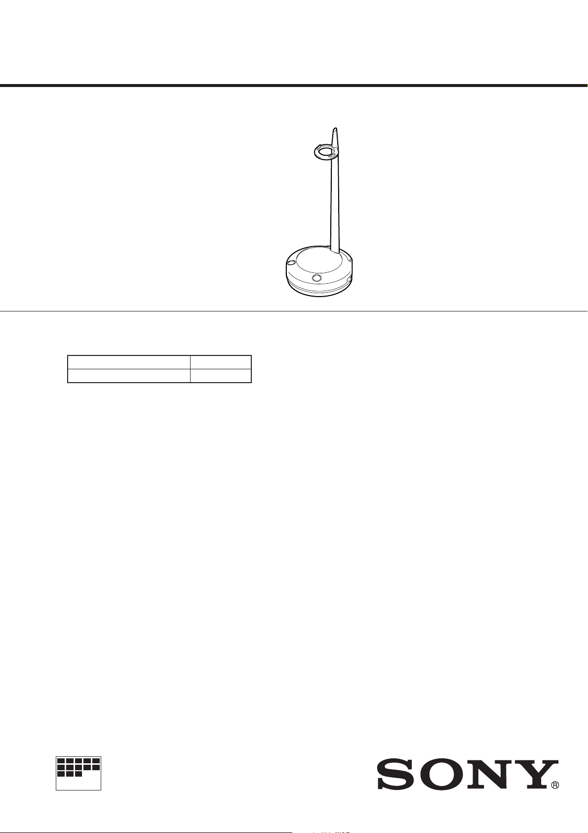
TMR-RF830R
SERVICE MANUAL
REVISED
Ver 1.2 1999. 09
TMR-RF830R is the component model block one in MDR-RF830RK.
COMPONENT MODEL NAME FOR MDR-RF830RK
Wireless Stereo Headphones MDR-RF830
Transmitter TMR-RF830R
SPECIFICATIONS
AEP Model
UK Model
General
Carrier frequency
Channel Ch1, Ch2
Modulation FM stereo
Frequency response
Transmitter
Power source DC 9 V: supplied AC power adaptor
Audio input phono jacks/stereo mini jack
Dimensions Approx. 120 mm dia × 290 mm
Mass Approx. 155 g (5.5 oz.)
Design and specifications are subject to change
without notice.
863.32 – 863.67 MHz
20 – 20,000 Hz
(43/4 × 111/2 in.)(w/h)
MICROFILM
TRANSMITTER
Page 2
SECTION 1
)
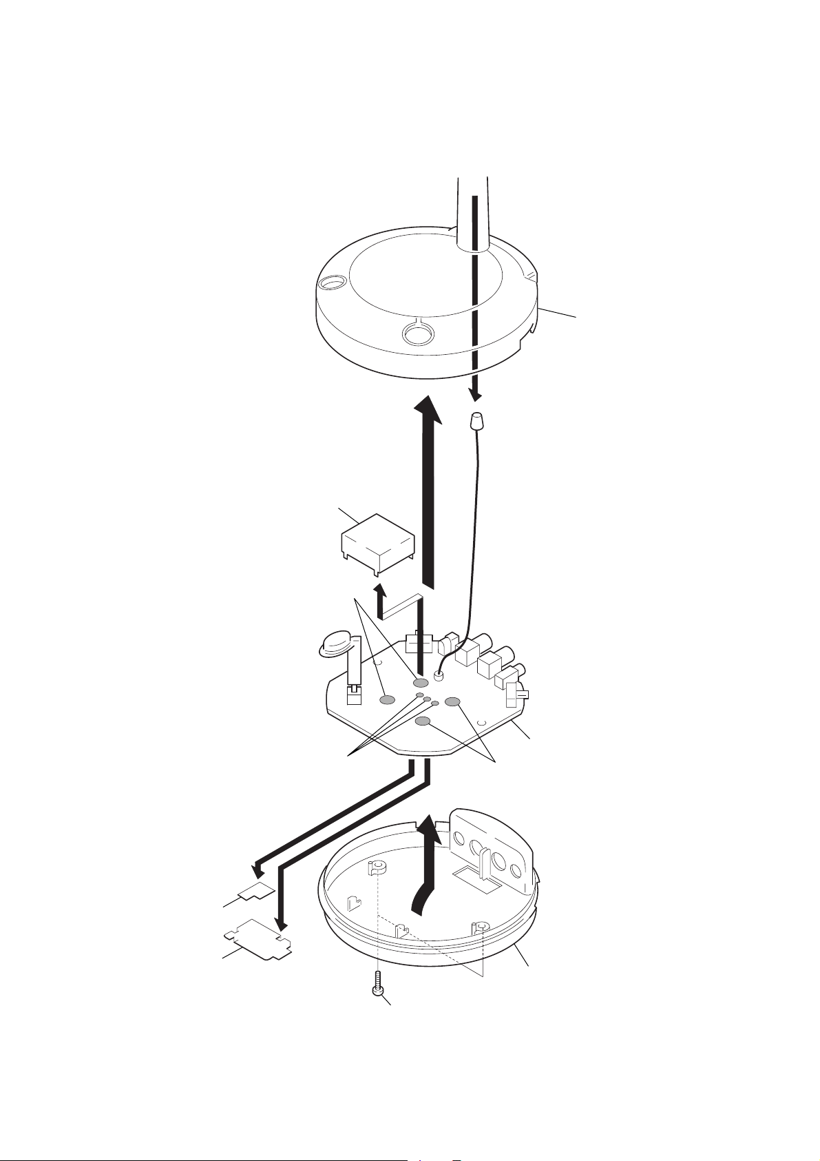
DISASSEMBLY
Note : Follow the disassembly procedure in the numerical order given.
1-1. TX BOARD, VCO BLOCK
Cabinet (Upper
3
2
Vco block
7
Remove
solder
8
Remove solder
9
TX board
7
Remove solder
6
TX shield plate
5
TX shield plate
1
— 2 —
4
Screws +P2 × 10
Cabinet (Lower)
Page 3
SECTION 2
t
ELECTRICAL ADJUSTMENTS
TMR-RF830R
Note :
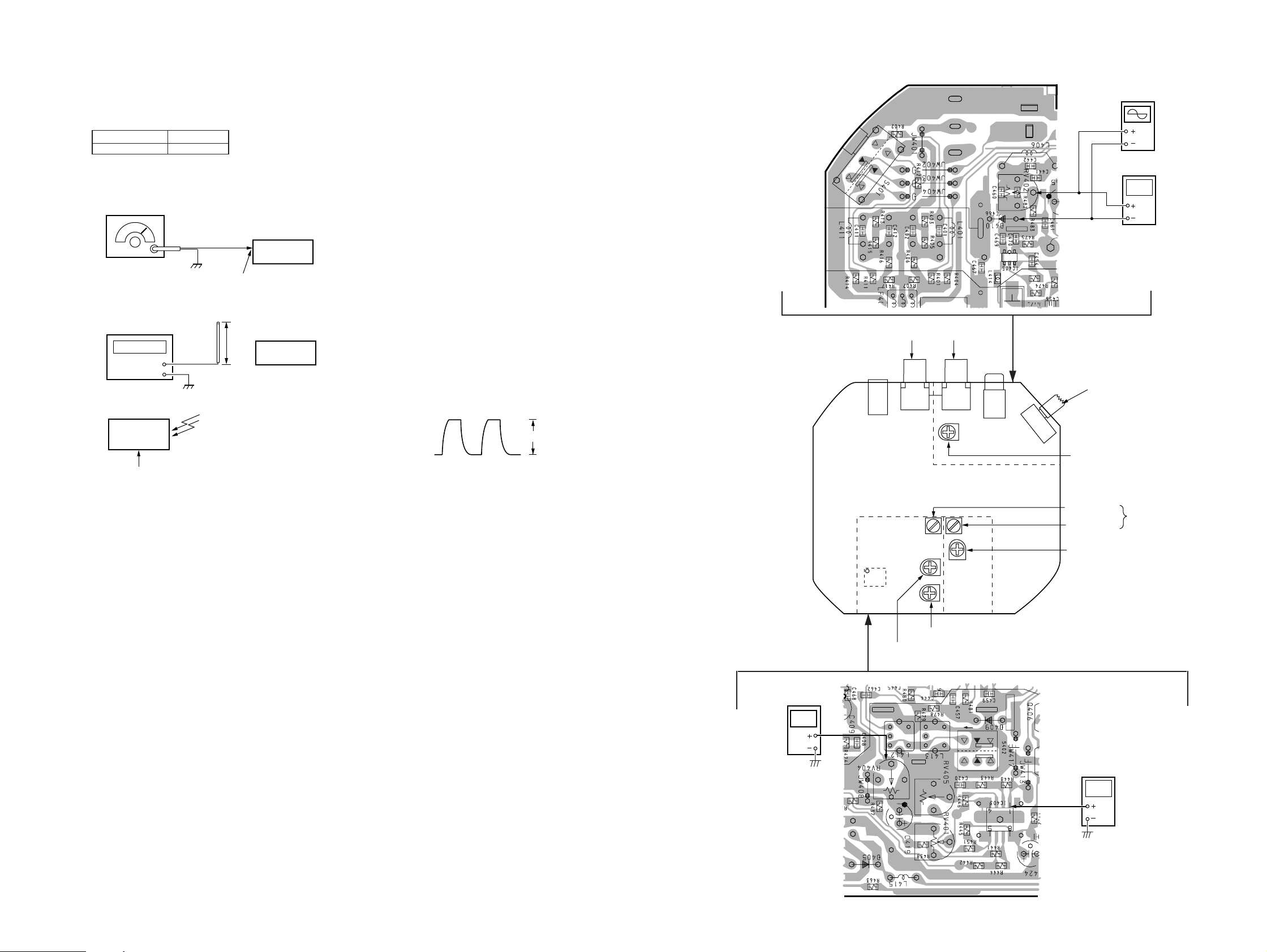
1. The transmitter section adjustments should be completed before performing the headphones section adjustment.
2. On adjusting the transmitter section, use the headphones as a jig.
Transmitter
TMR-RF830R
Headphones
MDR-RF830
Setting :
AF signal
generator
set
TMR-RF830R
L-CH (J403)
Telescopic
antenna
Frequency counter
8 cm
Headphones
set
TMR-RF830R
1. Set the noise filter SW to OFF.
2. Set the channel to CH2.
3. Input a signal of 1 kHz 316 mVrms to the L-CH (J403).
4. Measure the pin 1 voltage of the TX board IC403 using an
digital voltmeter (AC range) and make sure the value is 220 to
250 mVrms. If the measured value is other than the specified
value, adjust to 235mVrms by turning the RV401 on the TX
board.
Connection points and Adjustment Location :
TX board (See page 4)
Sub-Carrier Frequency/Level Check and Adjustment
1. Set the noise filter SW to OFF.
2. Set the channel to CH2.
3. Input a signal of 1 kHz 316 mVrms to only the L-CH (J403).
4. Connect a frequency counter and an oscilloscope between the
pin 2 of RV402 and GND.
5. Set the TX board L-CH (J403) input to OFF (not doing so will
cause modulation in the sub-carrier, preventing correct measurement)
6. Check to make sure the frequency counter reading is 49 to
51kHz. If the measured value is other than the specified v alue,
adjust the frequency to 50 kHz by turning the R V405 on the TX
board. In addition, check to make sure the oscilloscope waveform is as follows :
[TX BOARD] (Component side)Sub-Carrier (L-R) Modulation Check and Adjustment
Oscilloscope
-2
-1
45
13
J403
(L-CH)
J402
(R-CH)
Frequency counter
Sub-Carrier
Frequency
Adjustment
S401
Noise Filter ON/OFF Switch
MDR-RF830
Battery terminal (DC 3V)
Send Frequency Check and Adjustment
1. Set the noise filter SW to OFF.
2. Input a signal of 1 kHz 40 mVrms to only the L-CH (J403).
3. Connect a telescopic antenna to the frequency counter input
and extend the antenna to a length of approximately 8 cm.
4. Place TX board close to the frequency counter, then measure
the frequencies of CH1 and CH2 and make sure the values are
as follows:
CH1 : 863.27 to 863.37 MHz
CH2 : 863.62 to 863.72 MHz
When the frequency is not satisfied the specified value, first
set the channel switch (S402) to “2” and adjust CH2 frequency
with L412, next set it to “1” and adjust CH1 frequency with
L413. When completed with adjustment, recheck the frequecies
of CH1 and CH2.
Main-Carrier (L+R) Modulation Check and Adjustment
1. Set the noise filter SW to off.
2. Set the channel to CH2.
3. Input a signal of 1 kHz 316 Vrms to the L-ch (J403) and the RCH.(J402)
4. Measure the pin 2 voltage of the TX board RV 404 using a
digital voltmeter (AC range) and make sure the value is 75 to
95 mVrms. If the measured value is other than the specified
value, adjust to 85mVrms by turning the RV 404 on the TX
board.
80 – 100mVp-p
7. When the waveform P-P level is not satisf ied the specified value,
adjust to 90mVp-p with RV402.
(Perform the check and adjustment within one minute since the
transmitter A UTO OFF function will be acti vated approximately
one minute after setting the transmitter L-ch input to OFF. If
the A UT O OFF function activ ates, set the L-ch input to ON, set
TX board to AUTO ON, set the L-ch input again to OFF, then
make the check adjustment.)
Connection points and Adjustment Location :
TX board (See page 4)
Digital voltmeter
(AC range)
Main-Carrier (L+R)
Modulation Adjustment
RV401 : Sub-Carrier (L– R) Modulation Adjustment
RV405 : Sub-Carrier Frequency Adjustment
CHANNEL
1
2
-1 -2
RV402
Sub-Carrier Level Adjustment
L413 (CH1)
L412 (CH2)
RV404 : Main-Carrier (L+R)
Modulation Adjustment
Sub-Carrier (L-R)
Modulation Adjustmen
Digital voltmeter
(AC range)
Send Frequency
Adjustment
Connection points and Adjustment Location :
TX board (See page 4)
— 3 — — 4 —
Page 4

TMR-RF830R
3-1. PRINTED WIRING BOARD
SECTION 3
DIAGRAMS
• Semiconductor
Location
Ref. No. Location
D401 B-6
D402 B-7
D404 E-7
D405 E-7
D406 B-5
D407 C-5
D408 D-5
D409 D-6
D410 C-6
D411 E-4
IC401 F-6
IC402 C-6
IC403 C-7
IC404 D-5
IC405 E-4
Q401 F-7
Q403 B-5
Q404 B-5
Q405 B-4
Q406 C-6
Q407 C-4
Q408 C-4
Q409 C-3
A
B
C
D
12
TX BOARD
J404
DC IN 9V
ANT401
FM
WIRE
ANTENNA
AUDIO
IN
J403
L
A
R
J402
L408
345678910
POWER
OFF
-2
ON
-1
3
2
CHANNEL
1
2
3
45
1
2
-1 -2
VCO BLOCK
3
2
1
NOTE:
THE VCO BLOCK IS SUPPLIED
AS A UNIT FOR SERVICE.
Note:
• X : parts extracted from the component side.
p
•
•
• b : Pattern from the side which enables seeing.
Caution:
Pattern face side: Parts on the pattern face side seen from
(SideB) the pattern face are indicated.
Parts face side: Parts on the parts face side seen from
(Side A) the parts face are indicated.
: parts mounted on the conductor side.
®
: Through hole.
E
F
G
H
13
B
J401
-1
-2
RECHARGEABLE
BATTERY
Ni-Cd NC-AA(HJ) x 2
CHARGE TERMINAL
1-670-641-
11
(11)
16
S401
NOISE
FILTER
ON
OFF
I
— 5 — — 6 —
Page 5

3-2. SCHEMATIC DIAGRAM
TMR-RF830R
Note on Schematic Diagram:
• All capacitors are in µF unless otherwise noted. pF: µµF 50 WV
or less are not indicated except for electrolytics and tantalums.
• All resistors are in Ω and 1/
fied.
¢
•
• U : B+ Line.
• H : adjustment for repair.
•Power voltage is dc 3 V and fed with regulated dc power supply
: internal component.
from battery terminal.
4
W or less unless otherwise speci-
•Voltages are dc with respect to ground under no-signal conditions.
•Voltages are taken with a VOM (Input impedance 10 MΩ).
Voltage variations may be noted due to normal production tolerances.
•Waveforms are taken with a oscilloscope.
Voltage variations may be noted due to normal production tolerances.
• Circled numbers refer to waveforms.
• Signal path.
F
— 7 — — 8 —
WAVEFORM
r
1
VOL T/DIV : 0.2m V AC
TIME/DIV : 10 µsec
Page 6

TMR-RF830R
SECTION 4
EXPLODED VIEWS
TX
SECTION 5
ELECTRICAL PARTS LIST
NOTE:
• -XX, -X mean standardized parts, so they may
have some differences from the original one.
• Items marked “*” are not stocked since they
are seldom required for routine service. Some
delay should be anticipated when ordering these
items.
• The mechanical parts with no reference number
in the exploded views are not supplied.
7
1
6
8
12
5
not supplied
4
14
9
3
#2
not supplied
10
11
#2
13
2
#1
Ref. No. Part No. Description Remarks Ref. No. Part No. Description Remarks
1 4-984-729-01 FOOT, RUBBER
2 4-994-922-11 CABINET (LOWER)
3 4-994-931-01 BUTTON, POWER
4 4-993-652-01 BUTTON, OPEN
5 4-994-921-11 CABINET (UPPER)
6 4-994-923-01 LID, BATTERY CASE
7 4-994-925-01 CAP, ANTENNA
1
8 4-987-658-02 SPRING, BATTERY COIL
9 4-994-928-01 TERMINAL(+), CHARGE
10 4-994-930-01 TERMINAL(-), CHARGE
* 11 A-4542-539-A VCO BLOCK
* 12 4-994-924-01 PIPE, ANTENNA
* 13 A-4542-538-A TX BOARD, COMPLETE
14 4-213-544-01 CUSHION, ANTENNA
NOTE:
• Due to standardization, replacements in the
parts list may be different from the parts
specified in the diagrams or the components
used on the set.
• -XX, -X mean standardized parts, so they
may have some difference from the original
one.
• RESISTORS
All resistors are in ohms.
METAL: metal-film resistor
MET AL OXIDE: Metal Oxide-f ilm resistor
F: nonflammable
Ref. No. Part No. Description Remarks Ref. No. Part No. Description Remarks
* A-4542-538-A TX BOARD, COMPLETE
******************
4-994-928-01 TERMINAL (+), CHARGE
4-994-930-01 TERMINAL (-), CHARGE
< CAPACITOR >
C401 1-104-760-11 CERAMIC CHIP 0.047uF 10% 50V
C402 1-119-866-11 CERAMIC CHIP 0.68uF 10% 10V
C403 1-163-009-11 CERAMIC CHIP 0.001uF 10% 50V
C405 1-163-009-11 CERAMIC CHIP 0.001uF 10% 50V
C407 1-124-463-00 ELECT 0.1uF 20% 50V
C408 1-163-037-11 CERAMIC CHIP 0.022uF 10% 25V
C409 1-124-257-00 ELECT 2.2uF 20% 50V
C410 1-131-379-00 TANTALUM 22uF 10% 10V
C411 1-104-760-11 CERAMIC CHIP 0.047uF 10% 50V
C412 1-119-866-11 CERAMIC CHIP 0.68uF 10% 10V
C413 1-163-009-11 CERAMIC CHIP 0.001uF 10% 50V
C414 1-163-251-11 CERAMIC CHIP 100PF 5% 50V
C415 1-163-009-11 CERAMIC CHIP 0.001uF 10% 50V
C416 1-126-786-11 ELECT 47uF 20% 16V
C417 1-124-257-00 ELECT 2.2uF 20% 50V
C418 1-163-037-11 CERAMIC CHIP 0.022uF 10% 25V
C419 1-126-786-11 ELECT 47uF 20% 16V
C420 1-164-489-11 CERAMIC CHIP 0.22uF 10% 16V
C421 1-163-038-91 CERAMIC CHIP 0.1uF 25V
C422 1-163-131-00 CERAMIC CHIP 390PF 5% 50V
C423 1-163-131-00 CERAMIC CHIP 390PF 5% 50V
C424 1-126-786-11 ELECT 47uF 20% 16V
C425 1-163-131-00 CERAMIC CHIP 390PF 5% 50V
C426 1-126-786-11 ELECT 47uF 20% 16V
C427 1-163-021-91 CERAMIC CHIP 0.01uF 10% 50V
C428 1-126-382-11 ELECT 100uF 20% 16V
C429 1-163-012-00 CERAMIC CHIP 0.0018uF 5% 50V
C431 1-163-251-11 CERAMIC CHIP 100PF 5% 50V
C432 1-163-251-11 CERAMIC CHIP 100PF 5% 50V
C433 1-163-021-91 CERAMIC CHIP 0.01uF 10% 50V
C434 1-163-037-11 CERAMIC CHIP 0.022uF 10% 25V
C435 1-126-786-11 ELECT 47uF 20% 16V
C436 1-126-162-11 ELECT 3.3uF 20% 50V
C437 1-124-261-00 ELECT 10uF 20% 50V
C438 1-164-182-11 CERAMIC CHIP 0.0033uF 10% 50V
C439 1-126-382-11 ELECT 100uF 20% 16V
C440 1-124-234-00 ELECT 22uF 20% 16V
C441 1-163-009-11 CERAMIC CHIP 0.001uF 10% 50V
C442 1-163-251-11 CERAMIC CHIP 100PF 5% 50V
C443 1-163-009-11 CERAMIC CHIP 0.001uF 10% 50V
• Items marked “*” are not stocked since they
are seldom required for routine service.
Some delay should be anticipated when
ordering these items.
• SEMICONDUCTORS
In each case, u: µ, for example:
uA...: µA... , uPA... , µPA... ,
uPB... , µPB... , uPC... , µPC... ,
uPD..., µPD...
• CAPACITORS:
uF: µF
• COILS
uH: µH
C444 1-163-251-11 CERAMIC CHIP 100PF 5% 50V
C445 1-162-188-31 CERAMIC CHIP 1.2PF 20% 50V
C446 1-163-021-91 CERAMIC CHIP 0.01uF 10% 50V
C447 1-163-021-91 CERAMIC CHIP 0.01uF 10% 50V
C448 1-163-021-91 CERAMIC CHIP 0.01uF 10% 50V
C449 1-163-222-11 CERAMIC CHIP 5PF 0.25PF 50V
C451 1-163-085-00 CERAMIC CHIP 2PF 50V
C452 1-163-251-11 CERAMIC CHIP 100PF 5% 50V
C453 1-163-021-91 CERAMIC CHIP 0.01uF 10% 50V
C454 1-163-021-91 CERAMIC CHIP 0.01uF 10% 50V
C456 1-163-009-11 CERAMIC CHIP 0.001uF 10% 50V
C457 1-163-038-91 CERAMIC CHIP 0.1uF 25V
C459 1-163-009-11 CERAMIC CHIP 0.001uF 10% 50V
C460 1-163-012-00 CERAMIC CHIP 0.0018uF 5% 50V
C461 1-163-038-91 CERAMIC CHIP 0.1uF 25V
C462 1-163-038-91 CERAMIC CHIP 0.1uF 25V
C463 1-163-251-11 CERAMIC CHIP 100PF 5% 50V
C464 1-163-251-11 CERAMIC CHIP 100PF 5% 50V
C465 1-163-251-11 CERAMIC CHIP 100PF 5% 50V
C466 1-163-251-11 CERAMIC CHIP 100PF 5% 50V
C467 1-163-251-11 CERAMIC CHIP 100PF 5% 50V
C468 1-163-251-11 CERAMIC CHIP 100PF 5% 50V
C469 1-163-251-11 CERAMIC CHIP 100PF 5% 50V
C470 1-163-251-11 CERAMIC CHIP 100PF 5% 50V
CT401 1-141-485-11 CAP, ADJ 5PF
D401 8-719-066-59 LED SA3511 (POWER ON)
D402 8-719-066-60 LED SM3511 (POWER OFF/CHG)
D404 8-719-991-33 DIODE 1SS133T-77
D405 8-719-991-33 DIODE 1SS133T-77
D406 8-719-109-85 DIODE RD5.1ES-B2
D407 8-719-991-33 DIODE 1SS133T-77
D408 8-719-939-02 DIODE SVC203CP
D409 8-719-991-33 DIODE 1SS133T-77
D410 8-719-923-91 DIODE MTZJ-T77-16A
D411 8-719-923-91 DIODE MTZJ-T77-16A
IC401 8-759-998-71 IC BA3308F
IC402 8-759-537-90 IC KIA78S05P-TP
IC403 8-759-701-39 IC NJM3404AM
IC404 8-759-546-09 IC MC13176DR2
IC405 8-759-243-19 IC TC7SU04F
When indicating parts by reference number,
please include the board name.
< TRIMMER >
< DIODE >
< IC >
— 9 — — 10 —
Page 7

Ref. No. Part No. Description Remarks Ref. No. Part No. Description Remarks
< JACK >
J401 1-764-270-11 JACK,STEREO MINIATURE(DIA.3.5)
(AUDIO IN B)
J402 1-784-910-11 JACK, PIN (AUDIO IN A R)
J403 1-784-910-21 JACK, PIN (AUDIO IN A L)
J404 1-573-667-11 JACK,DC (POLARITY UNIFIED TYPE) (DC IN 9V)
< COIL >
L401 1-408-096-00 INDUCTOR 470uH
L403 1-410-336-11 INDUCTOR 220uH
L406 1-410-171-11 INDUCTOR 1mH
L407 1-411-960-21 INDUCTOR 4.7nH
L408 1-500-567-11 INDUCTOR
L409 1-412-948-11 INDUCTOR 5.6uH
L410 1-500-419-21 FERRITE 0uH
L411 1-408-096-00 INDUCTOR 470uH
L412 1-416-804-11 COIL
L413 1-416-805-11 COIL
L414 1-500-419-21 FERRITE 0uH
L415 1-410-336-11 INDUCTOR 220uH
< LINE FILTER >
LF401 1-411-236-11 FILTER, EMI
LF402 1-403-601-21 FILTER, COMMON MODE
< TRANSISTOR >
Q401 8-729-119-78 TRANSISTOR 2SC403SP-51
Q403 8-729-045-02 TRANSISTOR KTC3200GR-AT
Q404 8-729-045-00 TRANSISTOR SBX1639-02
Q405 8-729-045-02 TRANSISTOR KTC3200GR-AT
Q406 8-729-045-00 TRANSISTOR SBX1639-02
Q407 8-729-045-02 TRANSISTOR KTC3200GR-AT
Q408 8-729-045-02 TRANSISTOR KTC3200GR-AT
Q409 8-729-045-02 TRANSISTOR KTC3200GR-AT
< RESISTOR >
R401 1-216-085-00 METAL CHIP 33K 5% 1/10W
R402 1-216-304-11 METAL CHIP 3.3 5% 1/10W
R403 1-216-025-91 RES,CHIP 100 5% 1/10W
R404 1-216-085-00 METAL CHIP 33K 5% 1/10W
R405 1-216-025-91 RES,CHIP 100 5% 1/10W
R406 1-216-085-00 METAL CHIP 33K 5% 1/10W
R407 1-216-049-91 RES,CHIP 1K 5% 1/10W
R408 1-216-049-91 RES,CHIP 1K 5% 1/10W
R409 1-216-057-00 METAL CHIP 2.2K 5% 1/10W
R410 1-216-065-91 RES,CHIP 4.7K 5% 1/10W
R411 1-216-085-00 METAL CHIP 33K 5% 1/10W
R412 1-216-304-11 METAL CHIP 3.3 5% 1/10W
R413 1-216-025-91 RES,CHIP 100 5% 1/10W
R414 1-216-085-00 METAL CHIP 33K 5% 1/10W
R415 1-216-025-91 RES,CHIP 100 5% 1/10W
R416 1-216-085-00 METAL CHIP 33K 5% 1/10W
R417 1-216-049-91 RES,CHIP 1K 5% 1/10W
R418 1-216-049-91 RES,CHIP 1K 5% 1/10W
R419 1-216-057-00 METAL CHIP 2.2K 5% 1/10W
R420 1-216-129-00 METAL CHIP 2.2M 5% 1/10W
R421 1-216-081-00 METAL CHIP 22K 5% 1/10W
R422 1-216-121-91 RES,CHIP 1M 5% 1/10W
R423 1-216-295-91 SHORT 0
R425 1-216-033-00 METAL CHIP 220 5% 1/10W
R426 1-216-061-00 METAL CHIP 3.3K 5% 1/10W
R427 1-216-097-91 RES,CHIP 100K 5% 1/10W
R428 1-216-115-00 METAL CHIP 560K 5% 1/10W
R429 1-216-089-91 RES,CHIP 47K 5% 1/10W
R430 1-216-133-00 METAL CHIP 3.3M 5% 1/10W
R431 1-216-097-91 RES,CHIP 100K 5% 1/10W
R432 1-216-081-00 METAL CHIP 22K 5% 1/10W
R433 1-216-097-91 RES,CHIP 100K 5% 1/10W
R435 1-216-033-00 METAL CHIP 220 5% 1/10W
R436 1-216-061-00 METAL CHIP 3.3K 5% 1/10W
R437 1-216-061-00 METAL CHIP 3.3K 5% 1/10W
R438 1-216-061-00 METAL CHIP 3.3K 5% 1/10W
R439 1-216-061-00 METAL CHIP 3.3K 5% 1/10W
R440 1-216-049-91 RES,CHIP 1K 5% 1/10W
R441 1-216-061-00 METAL CHIP 3.3K 5% 1/10W
R442 1-216-073-00 METAL CHIP 10K 5% 1/10W
R443 1-216-085-00 METAL CHIP 33K 5% 1/10W
R444 1-216-073-00 METAL CHIP 10K 5% 1/10W
R445 1-216-061-00 METAL CHIP 3.3K 5% 1/10W
R446 1-216-049-91 RES,CHIP 1K 5% 1/10W
R448 1-216-093-00 METAL CHIP 68K 5% 1/10W
R449 1-216-081-00 METAL CHIP 22K 5% 1/10W
R450 1-216-081-00 METAL CHIP 22K 5% 1/10W
R451 1-216-059-00 METAL CHIP 2.7K 5% 1/10W
R452 1-216-025-91 RES,CHIP 100 5% 1/10W
R454 1-216-057-00 METAL CHIP 2.2K 5% 1/10W
R455 1-216-057-00 METAL CHIP 2.2K 5% 1/10W
R456 1-216-057-00 METAL CHIP 2.2K 5% 1/10W
R457 1-216-025-91 RES,CHIP 100 5% 1/10W
R458 1-216-077-00 METAL CHIP 15K 5% 1/10W
R459 1-216-049-91 RES,CHIP 1K 5% 1/10W
R460 1-216-027-00 METAL CHIP 120 5% 1/10W
R461 1-216-043-91 RES,CHIP 560 5% 1/10W
R462 1-216-043-91 RES,CHIP 560 5% 1/10W
R463 1-216-037-00 METAL CHIP 330 5% 1/10W
R464 1-216-073-00 METAL CHIP 10K 5% 1/10W
R465 1-216-073-00 METAL CHIP 10K 5% 1/10W
R466 1-216-113-00 METAL CHIP 470K 5% 1/10W
R467 1-216-089-91 RES,CHIP 47K 5% 1/10W
R468 1-216-049-91 RES,CHIP 1K 5% 1/10W
R469 1-216-081-00 METAL CHIP 22K 5% 1/10W
R470 1-216-045-00 METAL CHIP 680 5% 1/10W
R471 1-216-025-91 RES,CHIP 100 5% 1/10W
R472 1-216-033-00 METAL CHIP 220 5% 1/10W
R473 1-216-097-91 RES,CHIP 100K 5% 1/10W
R474 1-216-079-00 METAL CHIP 18K 5% 1/10W
R475 1-216-073-00 METAL CHIP 10K 5% 1/10W
R476 1-216-068-00 METAL CHIP 6.2K 5% 1/10W
R477 1-216-089-91 RES,CHIP 47K 5% 1/10W
R478 1-216-083-00 METAL CHIP 27K 5% 1/10W
R479 1-216-089-91 RES,CHIP 47K 5% 1/10W
R480 1-216-057-00 METAL CHIP 2.2K 5% 1/10W
R481 1-216-083-00 METAL CHIP 27K 5% 1/10W
R482 1-216-049-91 RES,CHIP 1K 5% 1/10W
R483 1-216-073-00 METAL CHIP 10K 5% 1/10W
— 11 —
Page 8

TMR-RF830R
Ref. No. Part No. Description Remarks Ref. No. Part No. Description Remarks
< VARIABLE RESISTOR >
RV401 1-241-764-11 RES, ADJ, CERMET 10K
RV402 1-238-601-11 RES, ADJ, CARBON 22K
RV404 1-238-601-11 RES, ADJ, CARBON 22K
RV405 1-241-762-11 RES, ADJ, CERMET 2.2K
< SWITCH >
S401 1-771-374-11 SWITCH, SLIDE (2C-2P)(NOISE FILTER)
S402 1-692-729-11 SWITCH, SLIDE (CHANNEL)
S403 1-771-375-11 SWITCH, PUSH (POWER)
< VIBRATOR >
XC401 1-781-046-21 VIBRATOR, CRYSTAL
************************************************************
**************
HARDWARE LIST
**************
#1 7-685-106-19 SCREW +P2 × 10 TYPE2 NON-SLIT
#2 7-685-105-19 SCREW +P2 × 8 TYPE2 NON-SLIT
9-924-941-13
Sony Corporation
Personal Audio Company
— 12 —
Printed in Japan ©1999.8
99H1639-1
Published by General Engineering Dept.
 Loading...