

Page 1
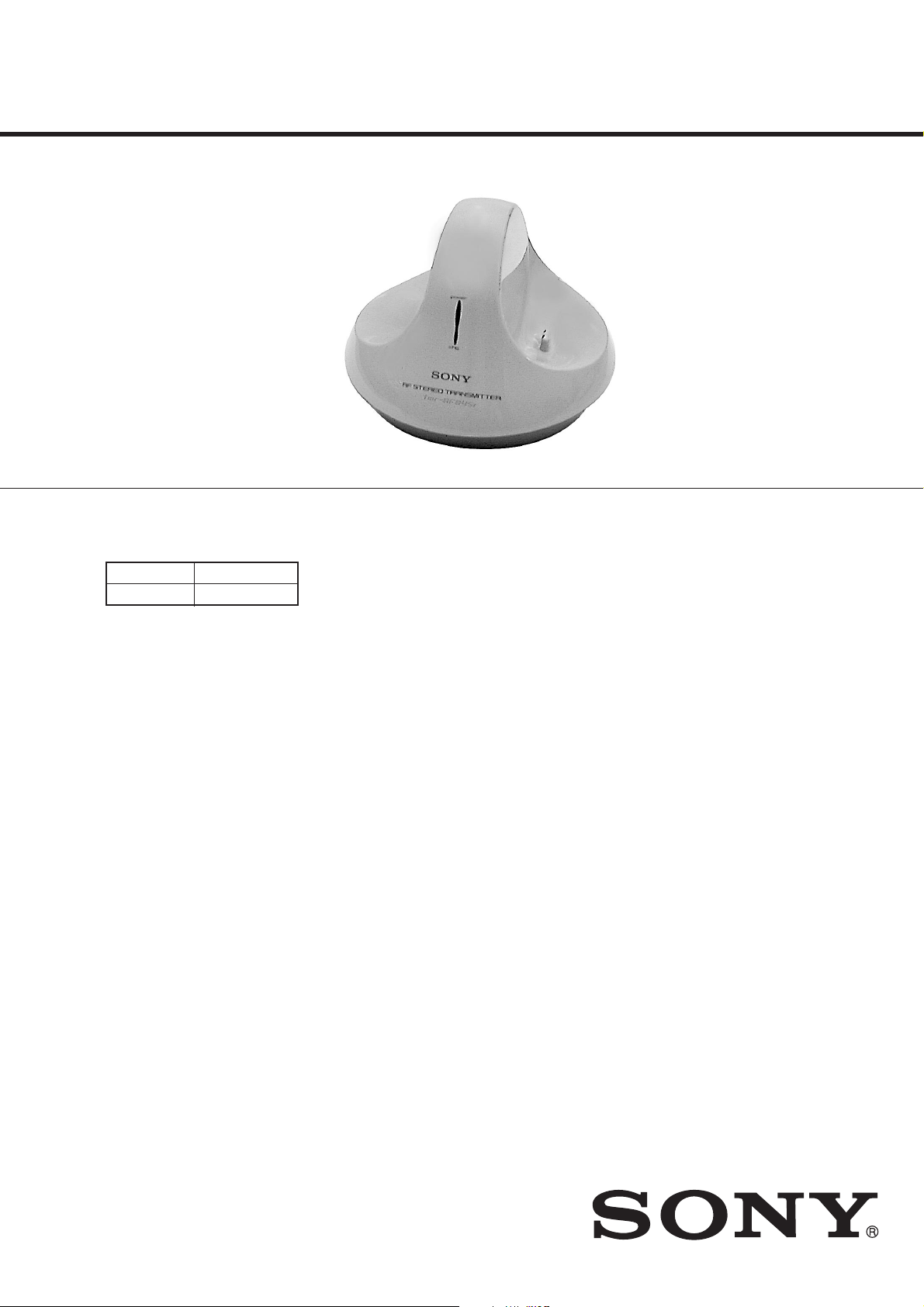
TMR-RF815R
SERVICE MANUAL
Ver 1.0 2000. 06
TMR-RF815R is the component model block one in the MDR-RF815RK.
COMPONENT MODEL NAME FOR MDR-RF815RK
Headphones MDR-RF815R
Transmitter TMR-RF815R
AEP Model
UK Model
SPECIFICATIONS
General
Carrier frequency
863.5 – 864.5 MHz
Channel Ch1, Ch2, Ch3
Modulation FM stereo
Frequency response
20 – 20,000 Hz
Transmitter
Power source DC 9 V: supplied AC power
adaptor
Audio input phono jacks/stereo mini jack
Dimensions Approx. 150 mm dia × 108 mm
(6 × 4 1/3 in.) (w/h)
Mass Approx. 190 g (6.2 oz.)
Design and specifications are subject to change without
notice.
TRANSMITTER
Page 2
Setting up the
SECTION 1
GENERAL
A To connect to a headphones jack
This section is extracted
from instruction manual.
transmitter
1
Connect the transmitter to audio/video
equipment. Select one of the hookups
below depending on the jack type:
Transmitter
OFF ON
FILTERNOISE
Right channel
(red)
Connecting cord
(supplied)
Unimatch plug
adaptor
(supplied)
to headphones
jack (stereo
phone jack)
RBAL
AUDIO IN
CD Walkman,
MD Walkman,
WALKMAN*,
VCR, etc.
to AUDIO IN
A jacks
DC IN 9V
123
CHANNEL
Left channel
(white)
to headphones
jack (stereo
mini jack)
SAFETY CHECK-OUT
After correcting the original service problem, perform the following
safety checks before releasing the set to the customer.
1. Check the area of your repair for unsoldered or poorlysoldered connections. Check the entire board surface
for solder splashes and bridges.
2. Check the interboard wiring to ensure that no wires are
"pinched" or contact high-wattage resistors.
3. Look for unauthorized replacement parts, particularly
transistors, that were installed during a previous repair.
Point them out to the customer and recommend their
replacement.
4. Look for parts which, through functioning, show obvious
signs of deterioration. Point them out to the customer
and recommend their replacement.
5. Check the B+ voltage to see it is at the values specified.
6. Flexible Circuit Board Repairing
• Keep the temperature of the soldering iron around 270˚C
during repairing.
• Do not touch the soldering iron on the same conductor
of the circuit board (within 3 times).
• Be careful not to apply force on the conductor when
soldering
— 2 —
Page 3
SECTION 2
r
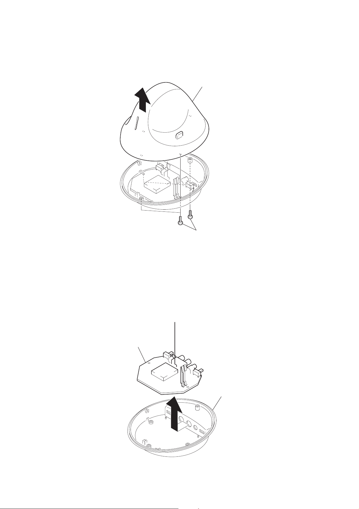
DISASSEMBLY
Note : Follow the disassembly procedure in the numerical order given.
2-1. CABINET (UPPER)
2
Cabinet (upper)
1
Four screws (P 2
× 8)
2-2. TX-BASE BOARD
2
TX-BASE board
Cabinet assy, lowe
1
— 3 —
Page 4

SECTION 3
ELECTRICAL ADJUSTMENTS
Setting :
AF signal
generator
set
TMR-RF815R
L-CH (J402)
Telescopic
antenna
Frequency counter
8 cm
set
TMR-RF815R
Send Frequency Check
1. Set the noise filter SW to OFF.
2. Input a signal of 1 kHz 40 mVrms to only the L-CH (J402).
3. Connect a telescopic antenna to the frequency counter input
and extend the antenna to a length of approximately 8 cm.
4. Place TX-BASE board close to the frequency counter , then measure the frequencies of CH1, CH2 and CH3 and make sure the
values are as follows:
CH1 : 863.5 MHz ± 40 kHz
CH2 : 864.0 MHz ± 40 kHz
CH3 : 864.5 MHz ± 40 kHz
Pilot signal Modulation Check and Adjustment
1. Set the channel to CH2.
2. No signal input (The operating time in this case is limited to 4
or 5 minutes.)
3. Measure the movable terminal of RV403 using an digital voltmeter (AC range) and make sure the v alue is 1.6mVrms ± 0.1mV.
If the measured value is other than the specified value, adjust to
1.6mVrms ± 0.1mV by turning the RV403 on the TX-BASE
board.
Connection points and Adjustment Location :
[TK-BASE BOARD] (Component side)
CH3
←
CH2 ←CH1
S402
RV403
(L-CH) (R-CH)
J402
VCO UNIT
When the frequency is not satisfied the specified v alue, exchange
vco unit. When completed with replacement, recheck the
frequecies of CH1, CH2 and CH3.
— 4 —
Page 5

4-1. BLOCK DIAGRAM
J401
B
AUDIO IN
J402
L
A
R R-CH
R-CH
S401
NOISE FILTER
OFF
|
ON
NOISE
FILTER
SECTION 4
DIAGRAMS
IC401
INPUT
AMP
LPF
R-CH
IC403
STEREO MPX
CH1
1 9
AMP
CH2
14
AMP
TIME
DEVISION
MPX
BUFFER
OSC
AMP
X401
38kHz
BUFFER
DIVIDER
76
TMR-RF815R
ANT401
RV403
MOD IN
8
VCO UNIT
ANT
T-OUT
IC405(2/2)
POWER OFF
DET
D402
IC402
5V
+5V
REG
SWITCH
Q404
D401
POWER
CHG
CHARGE
J404
DC IN 9V
B+
DI
CL
CE
IC405(1/2)
• Signal path.
16
: AUDIO
BUFFER
Q401
RECT
D404,405
INPUT
DET
15
13101211
DI
CL
CE
IC404
VCO CONTROLLER
679
1
2
3
VS
5V
CHANNEL
16
S402
2V
D408
+4V
Q402
Note on Printed Wiring Board:
• X : parts extracted from the component side.
• b : Pattern from the side which enables seeing.
Note on Schematic Diagram:
• All capacitors are in µF unless otherwise noted. pF: µµF 50 WV or
less are not indicated except for electrolytics and tantalums.
• All resistors are in Ω and 1/
f
•
: internal component.
4
W or less unless otherwise specified.
• A : B+ Line.
• H : adjustment for repair.
• Power voltage is dc 9 V and fed with regulated dc power supply
from battery terminal.
• V oltages are dc with respect to ground under no-signal conditions .
• Voltages are taken with a VOM (Input impedance 10 MΩ).
Voltage variations may be noted due to normal production tolerances.
• Waveforms are taken with a oscilloscope.
Voltage variations may be noted due to normal production tolerances.
• Circled numbers refer to waveforms.
• Signal path.
L: AUDIO
— 5 — — 6 —
Page 6

TMR-RF815R
4-2. SCHEMATIC DIAGRAM
220
330p 100k
— 7 — — 8 —
Page 7

4-3. PRINTED WIRING BOARD
TMR-RF815R
• Semiconductor
Location
Ref. No. Location
D401 D-3
D402 D-3
D403 A-4
D404 D-2
D405 D-2
D407 B-3
D408 D-4
D410 B-4
IC401 B-2
IC402 B-4
IC403 D-4
IC404 B-3
IC405 D-2
Q401 D-1
Q402 B-4
Q404 B-4
1
— 9 — — 10 —
Page 8

SECTION 5
EXPLODED VIEWS
TX-BASE
SECTION 6
ELECTRICAL PARTS LIST
NOTE:
• -XX, -X mean standardized parts, so they may
have some differences from the original one.
• Items marked “*” are not stocked since they
are seldom required for routine service. Some
delay should be anticipated when ordering these
items.
3
• The mechanical parts with no reference number
in the exploded views are not supplied.
• Accessories and packing materials are given in
the last of this parts list.
1
• Color Indication of Appearance Parts Example:
KNOB, BALANCE (WHITE) . . . (RED)
↑ ↑
Parts of Color Cabinet’s Color
2
8
NOTE:
• Due to standardization, replacements in the
parts list may be different from the parts
specified in the diagrams or the components
used on the set.
• -XX, -X mean standardized parts, so they
may have some difference from the original
one.
• Items marked “*” are not stocked since they
are seldom required for routine service.
Some delay should be anticipated when
ordering these items.
Ref. No. Part No. Description Remarks Ref. No. Part No. Description Remarks
* A-4542-645-A TX-BASE BOARD, COMPLETE
***********************
* A-4542-646-A TX-VCO UNIT (VCO)
< ANTENNA >
ANT401 4-213-164-01 TERMINAL, ANTENNA
< CAPACITOR >
C403 1-163-009-11 CERAMIC CHIP 0.001uF 10% 50V
C406 1-163-037-11 CERAMIC CHIP 0.022uF 10% 25V
C407 1-126-961-11 ELECT 2.2uF 20.00% 50V
C413 1-163-009-11 CERAMIC CHIP 0.001uF 10% 50V
C416 1-163-037-11 CERAMIC CHIP 0.022uF 10% 25V
• CAPACITORS:
uF: µF
• RESISTORS
All resistors are in ohms.
METAL: metal-film resistor
METAL OXIDE: Metal Oxide-film resistor
F: nonflammable
• COILS
uH: µH
C475 1-124-635-00 ELECT 220uF 20.00% 6.3V
C476 1-126-382-11 ELECT 100uF 20.00% 16V
C478 1-163-038-00 CERAMIC CHIP 0.1uF 25V
C480 1-163-021-91 CERAMIC CHIP 0.01uF 10.00% 50V
C481 1-163-251-11 CERAMIC CHIP 100PF 5.00% 50V
C483 1-163-224-11 CERAMIC CHIP 7PF 0.25PF 50V
C488 1-163-021-91 CERAMIC CHIP 0.01uF 10.00% 50V
D401 8-719-059-98 LED SLR-342VC3F (power)
D402 8-719-048-87 LED SLR-332MGF03 (chg)
D403 8-719-200-82 DIODE 11ES2
D404 8-719-991-33 DIODE 1SS133T-77
D405 8-719-991-33 DIODE 1SS133T-77
• SEMICONDUCTORS
In each case, u: µ, for example:
uA...: µA... , uPA... , µPA... ,
uPB... , µPB... , uPC... , µPC... ,
uPD..., µPD...
When indicating parts by reference number,
please include the board name.
< DIODE >
#2
4
5
#2
7
Ref. No. Part No. Description Remarks Ref. No. Part No. Description Remarks
1 3-046-687-11 CABINET (UPPER) (BLACK)
1 3-046-687-21 CABINET (UPPER) (WHITE)
2 3-049-800-01 CUSHION, ANTENNA
3 3-046-690-01 TUBE, LIGHT GUIDE
* 4 A-4542-645-A TX-BASE BOARD, COMPLETE
#2
5 X-3379-433-1 CABINET ASSY, LOWER (WHITE)
5 X-3379-660-1 CABINET ASSY, LOWER (BLACK)
7 4-984-729-01 FOOT, RUBBER
8 3-046-689-01 TERMINAL, CHARGE
#2 7-685-105-19 SCREW +P2X8 TYPE2 NON-SLIT
C417 1-126-961-11 ELECT 2.2uF 20.00% 50V
C421 1-124-234-00 ELECT 22uF 20% 16V
C422 1-126-934-11 ELECT 220uF 20.00% 16V
C423 1-163-251-11 CERAMIC CHIP 100PF 5.00% 50V
C425 1-163-037-11 CERAMIC CHIP 0.022uF 10% 25V
C426 1-163-021-91 CERAMIC CHIP 0.01uF 10.00% 50V
C427 1-163-021-91 CERAMIC CHIP 0.01uF 10.00% 50V
C428 1-163-251-11 CERAMIC CHIP 100PF 5.00% 50V
C429 1-163-251-11 CERAMIC CHIP 100PF 5.00% 50V
C430 1-124-259-11 ELECT 4.7uF 20.00% 16V
C431 1-126-157-11 ELECT 10uF 20% 16V
C432 1-163-018-00 CERAMIC CHIP 0.0056uF 5% 50V
C433 1-164-346-11 CERAMIC CHIP 1uF 16V
C435 1-163-038-00 CERAMIC CHIP 0.1uF 25V
C436 1-126-157-11 ELECT 10uF 20% 16V
C438 1-163-251-11 CERAMIC CHIP 100PF 5.00% 50V
C441 1-126-157-11 ELECT 10uF 20% 16V
C442 1-163-018-00 CERAMIC CHIP 0.0056uF 5% 50V
C443 1-164-346-11 CERAMIC CHIP 1uF 16V
C444 1-163-251-11 CERAMIC CHIP 100PF 5.00% 50V
C445 1-163-251-11 CERAMIC CHIP 100PF 5.00% 50V
C451 1-124-635-00 ELECT 220uF 20.00% 6.3V
C452 1-163-038-00 CERAMIC CHIP 0.1uF 25V
C453 1-126-157-11 ELECT 10uF 20% 16V
C454 1-163-251-11 CERAMIC CHIP 100PF 5.00% 50V
C455 1-163-227-11 CERAMIC CHIP 10PF 0.50PF 50V
C457 1-163-003-11 CERAMIC CHIP 330P 50V
C458 1-126-157-11 ELECT 10uF 20% 16V
C462 1-163-251-11 CERAMIC CHIP 100PF 5.00% 50V
C465 1-163-009-11 CERAMIC CHIP 0.001uF 10% 50V
D407 8-719-991-33 DIODE 1SS133T-77
D408 8-719-109-54 DIODE RD2.2ES-B2
D410 8-719-982-11 DIODE MTZJ-4.3B
< IC >
IC401 8-759-998-71 IC BA3308F
IC402 8-759-537-90 IC KIA78S05P-TP
IC403 8-759-667-59 IC NJM2035M(TE2)
IC404 8-759-679-76 IC KMP47C101M-1B54
IC405 8-759-510-73 IC BA10393F-E2
< JACK >
J401 1-566-822-21 JACK (B)
J402 1-580-441-61 JACK, PIN 2P (A)
J404 1-785-066-11 JACK,DC(POLARITY UNIFIED TYPE)(DC IN 9V)
< JUMPER >
JC418 1-216-295-91 SHORT 0
JC419 1-216-295-91 SHORT 0
JC421 1-216-295-91 SHORT 0
JC422 1-216-296-91 SHORT 0
JC423 1-216-296-91 SHORT 0
JC424 1-216-296-91 SHORT 0
JC426 1-216-296-91 SHORT 0
JC427 1-216-295-91 SHORT 0
JC430 1-216-295-91 SHORT 0
JC431 1-216-295-91 SHORT 0
JC470 1-216-295-91 SHORT 0
< COIL >
C466 1-163-021-91 CERAMIC CHIP 0.01uF 10.00% 50V
C468 1-163-038-00 CERAMIC CHIP 0.1uF 25V
C470 1-126-382-11 ELECT 100uF 20.00% 16V
C472 1-163-243-11 CERAMIC CHIP 47PF 5.00% 50V
C474 1-164-346-11 CERAMIC CHIP 1uF 16V
L401 1-414-234-11 INDUCTOR CHIP 0uH
L402 1-414-234-11 INDUCTOR CHIP 0uH
L404 1-414-234-11 INDUCTOR CHIP 0uH
L405 1-414-234-11 INDUCTOR CHIP 0uH
L408 1-419-079-21 COIL (MPX FILTER)
— 11 — — 12 —
Page 9

TX-BASE
Ref. No. Part No. Description Remarks Ref. No. Part No. Description Remarks
L409 1-419-079-21 COIL (MPX FILTER)
L410 1-419-662-31 COIL, AIR-CORE
L413 1-414-234-11 INDUCTOR CHIP 0uH
L414 1-414-234-11 INDUCTOR CHIP 0uH
L415 1-414-234-11 INDUCTOR CHIP 0uH
< TRANSISTOR >
Q401 8-729-230-49 TRANSISTOR 2SC2712-YG
Q402 8-729-230-49 TRANSISTOR 2SC2712-YG
Q404 8-729-045-00 TRANSISTOR KTA1266GR-AT
< RESISTOR >
R401 1-216-085-00 METAL CHIP 33K 5% 1/10W
R403 1-216-018-00 METAL CHIP 51 5% 1/10W
R404 1-216-085-00 METAL CHIP 33K 5% 1/10W
R406 1-216-085-00 METAL CHIP 33K 5% 1/10W
R407 1-216-049-91 RES-CHIP 1K 5% 1/10W
R408 1-216-057-00 METAL CHIP 2.2K 5% 1/10W
R411 1-216-085-00 METAL CHIP 33K 5% 1/10W
R413 1-216-018-00 METAL CHIP 51 5% 1/10W
R414 1-216-085-00 METAL CHIP 33K 5% 1/10W
R416 1-216-085-00 METAL CHIP 33K 5% 1/10W
R417 1-216-049-91 RES-CHIP 1K 5% 1/10W
R418 1-216-057-00 METAL CHIP 2.2K 5% 1/10W
R421 1-216-097-91 RES-CHIP 100K 5% 1/10W
R422 1-216-061-00 METAL CHIP 3.3K 5% 1/10W
R423 1-216-033-00 METAL CHIP 220 5% 1/10W
R424 1-216-133-00 METAL CHIP 3.3M 5% 1/10W
R425 1-216-097-91 RES-CHIP 100K 5% 1/10W
R426 1-216-061-00 METAL CHIP 3.3K 5% 1/10W
R427 1-216-033-00 METAL CHIP 220 5% 1/10W
R428 1-216-045-00 METAL CHIP 680 5% 1/10W
R429 1-216-073-00 METAL CHIP 10K 5% 1/10W
R430 1-216-073-00 METAL CHIP 10K 5% 1/10W
R431 1-216-065-91 RES-CHIP 4.7K 5% 1/10W
R432 1-216-129-00 METAL CHIP 2.2M 5% 1/10W
R433 1-216-081-00 METAL CHIP 22K 5% 1/10W
R434 1-216-105-91 RES-CHIP 220K 5% 1/10W
R463 1-216-085-00 METAL CHIP 33K 5% 1/10W
R464 1-216-061-00 METAL CHIP 3.3K 5% 1/10W
R466 1-216-081-00 METAL CHIP 22K 5% 1/10W
R467 1-216-065-00 METAL CHIP 4.7K 5% 1/10W
R469 1-216-097-11 METAL CHIP 100K 0.5% 1/10W
R472 1-216-186-00 RES-CHIP 330 5% 1/8W
R473 1-216-049-91 RES-CHIP 1K 5% 1/10W
R474 1-216-044-00 METAL CHIP 620 5% 1/10W
R475 1-216-051-00 METAL CHIP 1.2K 5% 1/10W
R476 1-216-051-00 METAL CHIP 1.2K 5% 1/10W
R477 1-216-051-00 METAL CHIP 1.2K 5% 1/10W
R478 1-216-051-00 METAL CHIP 1.2K 5% 1/10W
R479 1-216-051-00 METAL CHIP 1.2K 5% 1/10W
R481 1-216-067-11 METAL CHIP 5.6K 5% 1/10W
R482 1-216-081-00 METAL CHIP 22K 5% 1/10W
R483 1-216-081-00 METAL CHIP 22K 5% 1/10W
R484 1-216-081-00 METAL CHIP 22K 5% 1/10W
R485 1-216-081-00 METAL CHIP 22K 5% 1/10W
R486 1-216-081-00 METAL CHIP 22K 5% 1/10W
R489 1-216-079-91 METAL CHIP 18K 5% 1/10W
< VARIABLE RESISTOR >
RV403 1-241-763-11 RES, ADJ, CARBON 4.7K
< SWITCH >
S401 1-771-961-11 SWITCH, SLIDE (NOISE FILTER)
S402 1-771-962-11 SWITCH, SLIDE (CHANNEL)
< VIBRATOR >
X401 1-781-850-11 VIBRATOR, CRYSTAL 38kHz
*************************************************************
R438 1-216-105-91 RES-CHIP 220K 5% 1/10W
R440 1-216-049-91 RES-CHIP 1K 5% 1/10W
R441 1-216-033-00 METAL CHIP 220 5% 1/10W
R442 1-216-045-00 METAL CHIP 680 5% 1/10W
R446 1-216-051-00 METAL CHIP 1.2K 5% 1/10W
R447 1-216-214-00 RES-CHIP 4.7K 5% 1/8W
R448 1-216-049-91 RES-CHIP 1K 5% 1/10W
R449 1-216-081-00 METAL CHIP 22K 5% 1/10W
R451 1-216-073-00 METAL CHIP 10K 5% 1/10W
R452 1-216-077-00 RES-CHIP 15K 5% 1/10W
R453 1-216-073-00 METAL CHIP 10K 5% 1/10W
R454 1-216-073-00 METAL CHIP 10K 5% 1/10W
R455 1-216-077-00 RES-CHIP 15K 5% 1/10W
R456 1-216-051-00 METAL CHIP 1.2K 5% 1/10W
R457 1-216-214-00 RES-CHIP 4.7K 5% 1/8W
R458 1-216-049-91 RES-CHIP 1K 5% 1/10W
R459 1-216-081-00 METAL CHIP 22K 5% 1/10W
R460 1-216-086-00 RES-CHIP 36K 5% 1/10W
R461 1-216-091-00 METAL CHIP 56K 5% 1/10W
R462 1-216-121-91 RES-CHIP 1M 5% 1/10W
— 13 —
Page 10

TMR-RF815R
9-927-955-11
Sony Corporation
Audio Entertainment Group
— 14 —
Printed in Japan © 2000.6
2000F1646-1
Published by PE General Engineering Dept.
 Loading...