

Page 1
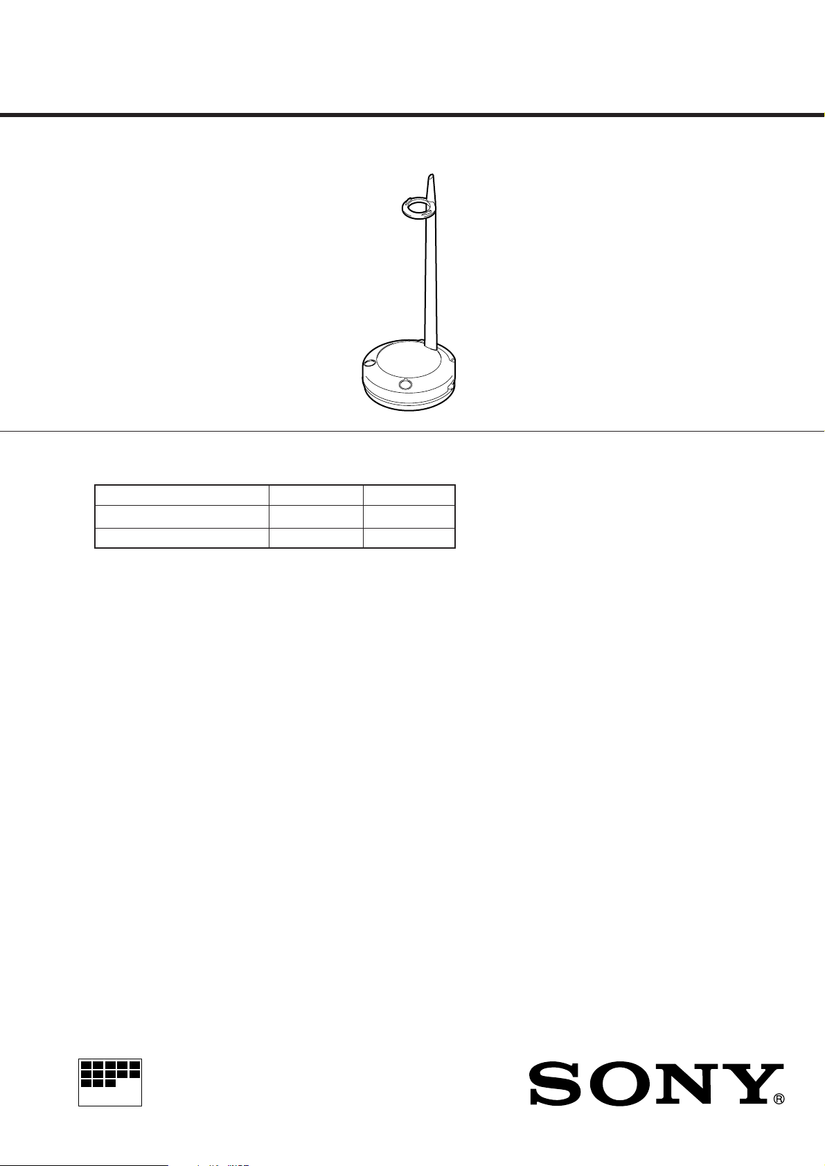
TMR-RF450R
SERVICE MANUAL
Ver 1.0 1998.06
TMR-RF450R is the component model block one in MDR-RF430RK/RF450RK.
COMPONENT MODEL NAME FOR MDR-RF430RK/RF450RK
MDR-RF430RK MDR-RF450RK
Wireless Stereo Headphones MDR-RF430 MDR-RF450
Transmitter TMR-RF450R TMR-RF450R
AEP Model
SPECIFICATIONS
General
Carrier frequency 433.40 – 434.40 MHz
Channel Ch1, Ch2, Ch3
Modulation FM stereo
Frequency response 20 – 20,000Hz (MDR-RF430RK)
Transmitter
Power source DC 9V : supplied AC power adaptor
Audio input Phono jacks / stereo mini jack
Dimensions Approx. 120 mm dia x 290 mm
Mass Approx. 155g (5.5oz.)
Design and specifications are subject to change without notice.
18 – 22,000Hz (MDR-RF450RK)
(4 3/4 x 11 1/2 in.) (w/h)
MICROFILM
RF STEREO TRANSMITTER
Page 2
SECTION 1
)
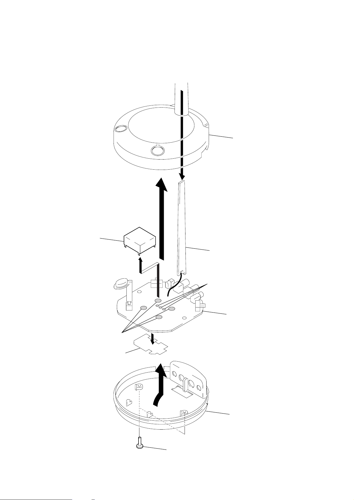
DISASSEMBLY
Note : Follow the disassembly procedure in the numerical order given.
1-1. TX BOARD REMOVAL
Cabinet (Upper
3
VCO board
6
Remove solder
5
TX shield plate
8
2
ANT board
7
Remove solder
TX board
4
– 2 –
1
Screws +P 2x10
Cabinet (Lower)
Page 3
SECTION 2
oscilloscope
digital voltmeter
(AC range)
ELECTRICAL ADJUSTMENTS
Note :
1. The transmitter section adjustments should be completed before
performing the headphones section adjustment.
2. On adjusting the transmitter section, use the headphones as a
jig.
Transmitter Headphones
TMR-RF450R
MDR-RF430
MDR-RF450
Setting :
AF signal
generator
set
TMR-RF450R
L-CH (J403)
telescopic
antenna
frequency counter
13cm
set
TMR-RF450R
Sub-Carrier Frequency Check and Adjustment
1. Set the noise filter SW to OFF.
2. Set the channel to CH2.
3. Input a signal of 1kHz 316mVrms to only the L-ch (J403).
4. Connect a frequency counter and an oscilloscope between the
Q409 emitter and GND.
5. Set the TX board L-ch (J403) input to OFF (not doing so will
cause modulation in the sub-carrier, pre venting correct measurement)
6. Check to make sure the frequency counter reading is 48 –52kHz.
If the measured value is other than the specified value, adjust
the frequency to 50kHz by turning the RV405 on the TX board.
In addition, check to make sure the oscilloscope waveform is as
follows :
3.4–3.8Vp-p
(Perform the check and adjustment within one minute since the
transmitter A UTO OFF function will be acti vated approximately
one minute after setting the transmitter L-ch input to OFF . If the
AUT O OFF function activates, set the L-ch input to ON, set TX
board to AUTO ON, set the L-ch input again to OFF, then make
the check adjustment.)
Connection points and Adjustment Location :
TX board (See page 4)
headphones
MDR-RF430
MDR-RF450
battery terminal (DC 3V)
Send Frequency Check and Adjustment
1. Set the noise filter SW to OFF.
2. Input a signal of 1kHz 40mVrms to only the L-ch (J403).
3. Connect a telescopic antenna to the frequency counter input and
extend the antenna to a length of approximately 13cm.
4. Place TX board close to the frequency counter , then measure the
frequencies of CH1, CH2 and CH3 and make sure the values are
as follows:
CH1 : 433.3 – 433.5MHz
CH2 : 433.8 – 434.0MHz
CH3 : 434.3 – 434.5MHz
If the measured values are other than the values specified above,
adjust the frequencies by turning RV402 and RV403 on the TX
board. When completed with adjustment, recheck the frequencies
of CH1, CH2 and CH3.
Connection points and Adjustment Location :
TX board (See page 4)
Sub-Carrier (L-R) Modulation Check and Adjustment
1. Set the noise filter SW to OFF.
2. Set the channel to CH2.
3. Input a signal of 1kHz 316mVrms to only the L-ch (J403).
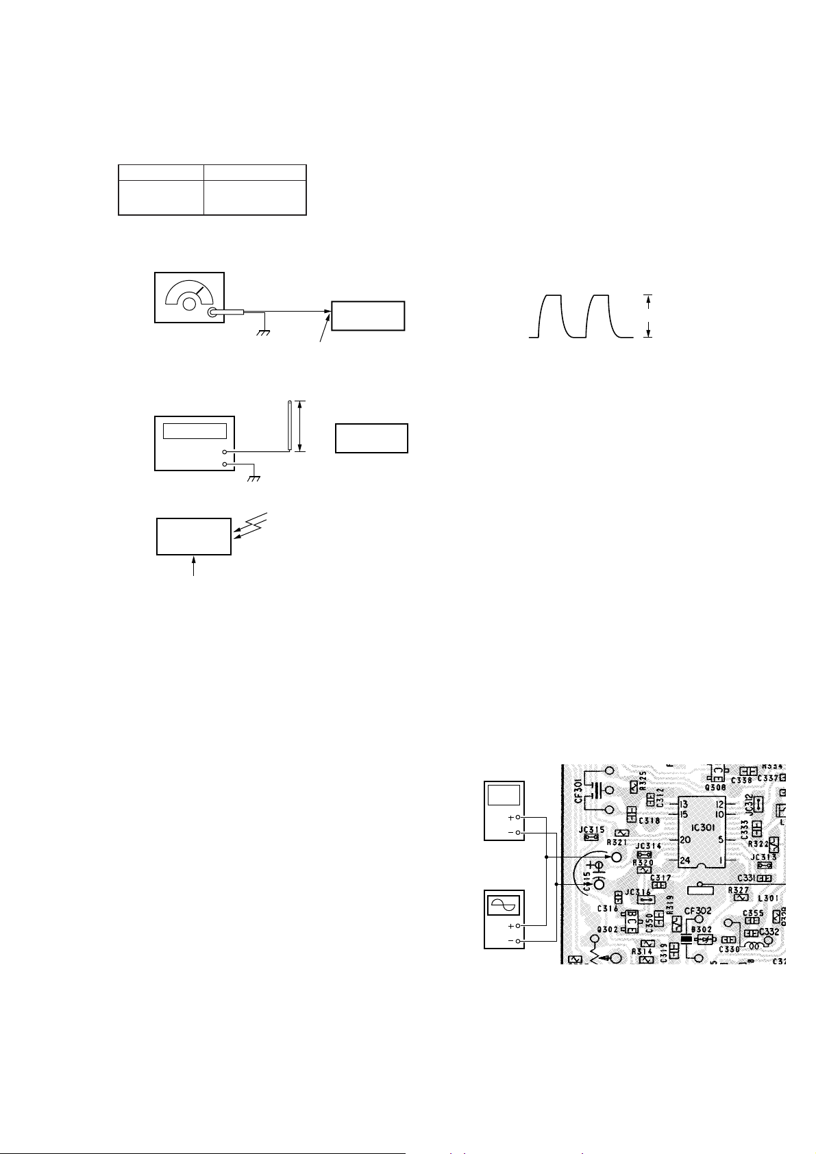
4. Measure the pin 1 voltage of the TX board IC403 using an
digital voltmeter (AC range) and make sure the value is 220 –
250mVrms. If the measured value is other than the specified
value, adjust to 235mVrms by turning the RV401 on the TX
board.
Main Carrier Modulation Check and Adjustment
1. Set the channel to CH2.
2. Set the noise filter SW to OFF.
3. Input a signal of 1kHz 316mVrms to only the transmitter Lch
(J403).
4. Set headphones VOL (RV301) to MIN.
5. Connect an digital voltmeter (AC range) and oscilloscope between IC301 pin @¡ and GND on RX board (headphones).
6. Receive signals by turning headphones TUNING V OL (R V302).
7. First check to make sure that a demodulated waveform of 1kHz
is outputted to the oscilloscope, then check to make sure the
digital voltmeter (AC range) reading is A C 12 –15mVrms. If the
reading is not within the specified range, turn RV404 on the TX
board so that the reading is 13.5mVrms.
HEADPHONES
[ RX BOARD ] (Conductor side)
Connection points and Adjustment Location :
TX board (See page 4)
Connection points and Adjustment Location :
TX board (See page 4)
– 3 –
Page 4

Connection points :
r
[ TX BOARD ] (Conductor side)
digital voltmeter
(AC range)
oscilloscope
Adjustment Location :
S402
Channel Select Switch
[TX BOARD] (Component side)
J403
(L-CH)
J402
(R-CH)
frequency counte
S401
Noise Filter ON/OFF Switch
RV402 (L-CH)
RV403 (R-CH)
Send Frequency
Adjustment
RV401 : Sub-Carrier (L– R) Modulation Adjustment
RV405 : Sub-Carrier Frequency Adjustment
– 4 –
RV404 : Main Carrier
Modulation Adjustment
Page 5

Page 6

Page 7

SECTION 4
EXPLODED VIEW
NOTE :
• -XX, -X mean standardized parts, so they
may have some difference from the original
one.
• Items marked “ * ”are not stocked since they
are seldom required for routine service. Some
delay should be anticipated when ordering
these items.
7
10
4
• The mechanical parts with no reference
number in the exploded views are not
supplied.
3
5
13
11
8
not supplied
6
15
9
L406
not supplied
12
12
16
14
not supplied
2
3
1
Ref. No. Part No. Description Remark Ref. No. Part No. Description Remark
1 7-685-106-19 SCREW +P 2X10 TYPE2 NON-SLIT
2 4-994-922-01 CABINET (LOWER)
3 4-984-729-01 FOOT, RUBBER
4 4-993-652-01 BUTTON, OPEN
5 4-994-931-01 BUTTON, POWER
6 4-987-658-02 SPRING, BATTERY COIL
7 4-994-923-01 LID, BATTERY CASE
8 4-994-925-01 CAP, ANTENNA
* 9 4-994-924-01 PIPE ANTENNA
10 4-994-921-01 CABINET (UPPER)
11 4-994-928-01 TERMINAL (+), CHARGE
12 7-685-105-19 SCREW +P 2X8 TYPE2 NON-SLIT
13 4-994-930-01 TERMINAL (-), CHARGE
* 14 A-4542-512-A TX BOARD, COMPLETE
15 1-670-934-11 ANT BOARD
* 16 A-4542-532-A VCO BOARD, COMPLETE
L406 1-500-549-11 CORE, FERRITE
– 7 –
Page 8

SECTION 5
ANT
NOTE :
• Due to standardization, replacements in the
parts list may be different from the parts
specified in the diagrams or the components
used on the set.
• -XX, -X mean standardized parts, so they
may have some difference from the original
one.
• RESISTORS
All resistors are in ohms
METAL : Metal-film resistor
METAL OXIDE :Metal oxide-film resistor
F : nonflammable
Ref. No. Part No. Description Remark Ref. No. Part No. Description Remark
************************************************************
TX
1-670-934-11 ANT BOARD
**********
ELECTRICAL PARTS LIST
• Items marked “ * ”are not stocked since they
are seldom required for routine service. Some
delay should be anticipated when ordering
these items.
• SEMICONDUCTORS
In each case, u : µ , for example :
uA.... : µ A.... , uPA.... : µ PA....
uPB.... : µ PB.... , uPC.... : µ PC....
uPD.... : µ PD....
• CAPACITORS
uF : µ F
• COILS
uH : µ H
C439 1-126-382-11 ELECT 100uF 20% 16V
C440 1-126-786-11 ELECT 47uF 20% 16V
C441 1-163-021-91 CERAMIC CHIP 0.01uF 10% 50V
When indicating parts by reference number, please include the board.
* A-4542-512-A TX BOARD, COMPLETE
*******************
4-994-928-01 TERMINAL (+), CHARGE
4-994-930-01 TERMINAL (-), CHARGE
< CAPACITOR >
C401 1-104-760-11 CERAMIC CHIP 0.047uF 10% 50V
C402 1-119-866-11 CERAMIC CHIP 0.68uF 10% 10V
C403 1-163-009-11 CERAMIC CHIP 0.001uF 10% 50V
C405 1-163-009-11 CERAMIC CHIP 0.001uF 10% 50V
C407 1-124-463-00 ELECT 0.1uF 20% 50V
C408 1-163-037-11 CERAMIC CHIP 0.022uF 10% 25V
C409 1-124-257-00 ELECT 2.2uF 20% 50V
C410 1-131-379-00 TANTALUM 22uF 10% 10V
C411 1-104-760-11 CERAMIC CHIP 0.047uF 10% 50V
C412 1-119-866-11 CERAMIC CHIP 0.68uF 10% 10V
C413 1-163-009-11 CERAMIC CHIP 0.001uF 10% 50V
C414 1-163-251-11 CERAMIC CHIP 100PF 5% 50V
C415 1-163-009-11 CERAMIC CHIP 0.001uF 10% 50V
C416 1-126-786-11 ELECT 47uF 20% 16V
C417 1-124-257-00 ELECT 2.2uF 20% 50V
C418 1-163-037-11 CERAMIC CHIP 0.022uF 10% 25V
C419 1-126-786-11 ELECT 47uF 20% 16V
C420 1-124-464-11 ELECT 0.22uF 20% 50V
C421 1-163-038-91 CERAMIC CHIP 0.1uF 25V
C422 1-163-131-00 CERAMIC CHIP 390PF 5% 50V
< TRIMMER >
CT401 1-141-486-11 CAP, ADJ 10PF
< DIODE >
D401 8-719-066-59 LED SA3511 (POWER Ø ON)
D402 8-719-066-60 LED SM3511 (POWER ø OFF/CHG)
D404 8-719-991-33 DIODE 1SS133T-77
D405 8-719-991-33 DIODE 1SS133T-77
D406 8-719-109-85 DIODE RD5.1ES-B2
D407 8-719-991-33 DIODE 1SS133T-77
D408 8-719-991-33 DIODE 1SS133T-77
< IC >
IC401 8-759-998-71 IC BA3308F
IC402 8-759-537-90 IC KIA78S05P-TP
IC403 8-759-701-39 IC NJM3404AM
< JACK >
J401 1-764-270-11 JACK,STEREO MINIATURE(DIA.3.5)
(AUDIO IN B)
J402 1-784-910-11 JACK, PIN (AUDIO IN A R)
J403 1-784-910-21 JACK, PIN (AUDIO IN A L)
J404 1-573-667-11 JACK,DC(POLARITY UNIFIED TYPE)
(DC IN 9V)
< COIL >
C423 1-163-131-00 CERAMIC CHIP 390PF 5% 50V
C424 1-124-257-00 ELECT 2.2uF 20% 50V
C425 1-163-135-00 CERAMIC CHIP 560PF 5% 50V
C426 1-126-786-11 ELECT 47uF 20% 16V
C427 1-163-021-91 CERAMIC CHIP 0.01uF 10% 50V
C428 1-126-382-11 ELECT 100uF 20% 16V
C430 1-163-251-11 CERAMIC CHIP 100PF 5% 50V
C431 1-163-251-11 CERAMIC CHIP 100PF 5% 50V
C432 1-163-251-11 CERAMIC CHIP 100PF 5% 50V
C433 1-163-021-91 CERAMIC CHIP 0.01uF 10% 50V
C434 1-163-037-11 CERAMIC CHIP 0.022uF 10% 25V
C435 1-126-786-11 ELECT 47uF 20% 16V
C436 1-126-162-11 ELECT 3.3uF 20% 50V
C437 1-124-261-00 ELECT 10uF 20% 50V
C438 1-164-182-11 CERAMIC CHIP 0.0033uF 10% 50V
L401 1-408-096-00 INDUCTOR 470uH
L403 1-410-336-31 INDUCTOR 220uH
L404 1-500-419-21 INDUCTOR, FERRITE BEAD
L405 1-500-419-21 INDUCTOR, FERRITE BEAD
L406 1-500-549-11 CORE, FERRITE
L411 1-408-096-00 INDUCTOR 470uH
< LINE FILTER >
LF401 1-411-236-11 FILTER, EMI
LF402 1-403-601-21 FILTER
< TRANSISTOR >
Q401 8-729-119-78 TRANSISTOR 2SC403SP-51
Q403 8-729-045-02 TRANSISTOR KTC3200GR-AT
– 8 –
Page 9

TX
Ref. No. Part No. Description Remark Ref. No. Part No. Description Remark
Q404 8-729-045-00 TRANSISTOR SBX1639-02
Q405 8-729-045-02 TRANSISTOR KTC3200GR-AT
Q406 8-729-045-00 TRANSISTOR SBX1639-02
Q407 8-729-045-02 TRANSISTOR KTC3200GR-AT
Q408 8-729-045-02 TRANSISTOR KTC3200GR-AT
Q409 8-729-045-02 TRANSISTOR KTC3200GR-AT
< RESISTOR >
R401 1-216-085-00 METAL CHIP 33K 5% 1/10W
R402 1-216-304-11 METAL CHIP 3.3 5% 1/10W
R403 1-216-025-91 RES,CHIP 100 5% 1/10W
R404 1-216-085-00 METAL CHIP 33K 5% 1/10W
R405 1-216-025-91 RES,CHIP 100 5% 1/10W
R406 1-216-085-00 METAL CHIP 33K 5% 1/10W
R407 1-216-049-91 RES,CHIP 1K 5% 1/10W
R408 1-216-049-91 RES,CHIP 1K 5% 1/10W
R409 1-216-057-00 METAL CHIP 2.2K 5% 1/10W
R410 1-216-065-91 RES,CHIP 4.7K 5% 1/10W
R455 1-216-057-00 METAL CHIP 2.2K 5% 1/10W
R456 1-216-057-00 METAL CHIP 2.2K 5% 1/10W
R457 1-216-025-91 RES,CHIP 100 5% 1/10W
R458 1-216-085-00 METAL CHIP 33K 5% 1/10W
R460 1-216-029-00 METAL CHIP 150 5% 1/10W
R461 1-216-043-91 RES,CHIP 560 5% 1/10W
R462 1-216-043-91 RES,CHIP 560 5% 1/10W
R463 1-216-037-00 METAL CHIP 330 5% 1/10W
R464 1-216-073-00 METAL CHIP 10K 5% 1/10W
R465 1-216-073-00 METAL CHIP 10K 5% 1/10W
R466 1-216-113-00 METAL CHIP 470K 5% 1/10W
R467 1-216-089-91 RES,CHIP 47K 5% 1/10W
R468 1-216-049-91 RES,CHIP 1K 5% 1/10W
R469 1-216-081-00 METAL CHIP 22K 5% 1/10W
R470 1-216-045-00 METAL CHIP 680 5% 1/10W
< JUMPER RESISTOR >
R423 1-216-295-00 METAL CHIP 0 5% 1/10W
VCO
R411 1-216-085-00 METAL CHIP 33K 5% 1/10W
R412 1-216-304-11 METAL CHIP 3.3 5% 1/10W
R413 1-216-025-91 RES,CHIP 100 5% 1/10W
R414 1-216-085-00 METAL CHIP 33K 5% 1/10W
R415 1-216-025-91 RES,CHIP 100 5% 1/10W
R416 1-216-085-00 METAL CHIP 33K 5% 1/10W
R417 1-216-049-91 RES,CHIP 1K 5% 1/10W
R418 1-216-049-91 RES,CHIP 1K 5% 1/10W
R419 1-216-057-00 METAL CHIP 2.2K 5% 1/10W
R420 1-216-129-00 METAL CHIP 2.2M 5% 1/10W
R421 1-216-081-00 METAL CHIP 22K 5% 1/10W
R422 1-216-121-91 RES,CHIP 1M 5% 1/10W
R425 1-216-033-00 METAL CHIP 220 5% 1/10W
R426 1-216-061-00 METAL CHIP 3.3K 5% 1/10W
R427 1-216-097-91 RES,CHIP 100K 5% 1/10W
R428 1-216-115-00 METAL CHIP 560K 5% 1/10W
R429 1-216-089-91 RES,CHIP 47K 5% 1/10W
R430 1-216-133-00 METAL CHIP 3.3M 5% 1/10W
R431 1-216-097-91 RES,CHIP 100K 5% 1/10W
R432 1-216-081-00 METAL CHIP 22K 5% 1/10W
R433 1-216-097-91 RES,CHIP 100K 5% 1/10W
R435 1-216-033-00 METAL CHIP 220 5% 1/10W
R436 1-216-061-00 METAL CHIP 3.3K 5% 1/10W
R437 1-216-085-00 METAL CHIP 33K 5% 1/10W
R438 1-216-061-00 METAL CHIP 3.3K 5% 1/10W
< VARIABLE RESISTOR >
RV401 1-241-764-11 RES, ADJ, CERMET 10K
(SUB CARRIER (L-R) MODULATION FACTOR)
RV402 1-241-764-11 RES, ADJ, CERMET 10K (SEND FREQUENCY)
RV403 1-238-601-11 RES, ADJ, CARBON 22K (SEND FREQUENCY)
RV404 1-241-764-11 RES, ADJ, CERMET 10K
(MAIN CARRIER MODULATION)
RV405 1-241-762-11 RES, ADJ, CERMET 2.2K
(SUB CARRIER FREQUENCY)
< SWITCH >
S401 1-771-374-11 SWITCH, SLIDE (2C-2P) (NOISE FILTER)
S402 1-771-373-11 SWITCH, SLIDE (1C-3P) (CHANNEL)
S403 1-771-375-11 SWITCH, PUSH (POWER)
************************************************************
* A-4542-532-A VCO BOARD, COMPLETE
*********************
**************************************************************
MISCELLANEOUS
***************
L406 1-500-549-11 CORE, FERRITE
R439 1-216-085-00 METAL CHIP 33K 5% 1/10W
R440 1-216-049-91 RES,CHIP 1K 5% 1/10W
R441 1-216-061-00 METAL CHIP 3.3K 5% 1/10W
R442 1-216-073-00 METAL CHIP 10K 5% 1/10W
R443 1-216-085-00 METAL CHIP 33K 5% 1/10W
R444 1-216-073-00 METAL CHIP 10K 5% 1/10W
R445 1-216-061-00 METAL CHIP 3.3K 5% 1/10W
R446 1-216-049-91 RES,CHIP 1K 5% 1/10W
R447 1-216-051-00 METAL CHIP 1.2K 5% 1/10W
R448 1-216-093-00 METAL CHIP 68K 5% 1/10W
R449 1-216-081-00 METAL CHIP 22K 5% 1/10W
R450 1-216-081-00 METAL CHIP 22K 5% 1/10W
R451 1-216-061-00 METAL CHIP 3.3K 5% 1/10W
R452 1-216-081-00 METAL CHIP 22K 5% 1/10W
R454 1-216-057-00 METAL CHIP 2.2K 5% 1/10W
– 11 –
Page 10

TMR-RF450R
9-924-919-11
Sony Corporation
Personal A&V Products Company
– 12 –
Printed in Hungary © 1998.6
98F027539-1
Published by Quality Engineering Dept.
(Shibaura)
 Loading...