

Page 1
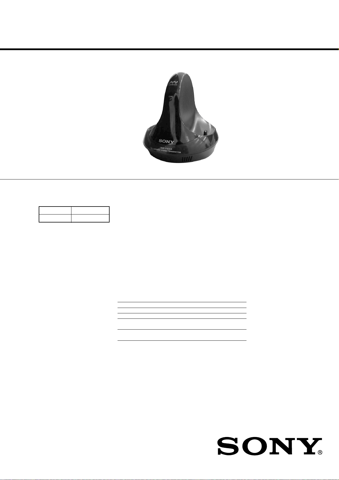
TMR-IF630R
SERVICE MANUAL
Ver 1.0 2000.12
TMR-IF630R is the component model block one in the MDR-IF630RK.
COMPONENT MODEL NAME FOR MDR-IF630RK
Headphones MDR-IF630R
Transmitter TMR-IF630R
US Model
AEP Model
UK Model
E Model
Tourist Model
SPECIFICATIONS
General
Modulation system Frequency modulation
Carrier frequency Right 2.8 MHz
Transmitter
Power source DC IN 9V jack accepts power supplied from the
Where purchased Operating voltage
U.S.A. 120 V AC, 60 Hz
U.K. 220 – 230 V AC, 50 Hz
European countries 220 – 230 V AC, 50 Hz
Japan (except for Japanese 110 V/120 V/220 V/240V AC, 50/60 Hz
domestic model)
Other countries 220 – 230 V AC, 50/60Hz or
Audio input Phono jacks/stereo mini jack
Dimensions Approx. 130 x 135 x 150 mm
Mass Approx. 200 g (7 oz)
Design and specifications are subject to change without notice.
Left 2.3 MHz
AC power adaptor for use on the follo wing v oltages:
120 V AC, 60 Hz
(5 1/4 x 5 3/8 x 6 in) (w/h/d)
TRANSMITTER
Page 2

Setting up the
transmitter
1
Connect the transmitter to audio/video
equipment. Select one of the hookups
below depending on the jack type:
To connect to a headphones jack
Set the INPUT SOURCE selector to
PHONES.
SECTION 1
GENERAL
ATT (attenuator) selector
If a loud sound is distorted when the transmitter
is connected to an audio output jack other than
the headphones jack, set the ATT selector on the
transmitter to -12 dB. The default setting of the
ATT selector is 0 dB.
ATT selector
ATT
–12dB0dB
This section is extracted
from instruction manual.
INPUT SOURCE
PHONESLINE
to AUDIO IN A jacks
Right channel
(red)
Connecting cord
(supplied)
Unimatch plug
adaptor
(supplied)
to headphones
jack (stereo
phone jack)
RBAL
AUDIO IN
to headphones
jack (stereo
mini jack)
Transmitter
DC IN 9V
Left channel
(white)
CD Walkman,
MD Walkman,
WALKMAN*,
TV, VCR, etc.
Flexible Circuit Board Repairing
• Keep the temperature of soldering iron around 270˚C
during repairing.
• Do not touch the soldering iron on the same conductor of the
circuit board (within 3 times).
• Be careful not to apply force on the conductor when soldering
or unsoldering.
Notes on chip component replacement
• Never reuse a disconnected chip component.
• Notice that the minus side of a tantalum capacitor may be
damaged by heat.
— 2 —
Page 3

SECTION 2
d
)
DISASSEMBLY
Note : The equipment can be removed using the following procedure.
Set
Cabinet (top) TX BASE boar
TX LED board
Note : Follow the disassembly procedure in the numerical order given.
2-1. CABINET (TOP) 2-2.TX BASE BOARD
3
Cabinet (top
2
TX BASE board
2
LED board (CN1)
1
Claw
2-3. TX LED BOARD
1
Four screws (+P 2
2
Window, luminous
×
8)
4
TX LED board
a
1
Two screws (+P 2 × 6)
3
a
Two screws (+P 2 × 6)
— 3 —
Page 4

SECTION 3
r
r
ELECTRICAL ADJUSTMENTS
Note :
1. The adjustments should be performed in the order given. (As a
general rule the transmitter section (TMR-IF630R) adjustments
should be completed before performing the headphones section (MDR-IF630R) adjustment.)
2. The adjustments and measurements should be performed for
both L-ch and R-ch unless otherwise indicated.
3. L-ch adjustment should be completed before performing R-ch
adjustment.
4. Supply 9 V dc to the transmitter section (TMR-IF630R) and
2.4 V dc to the headphones section (MDR-IF630R) as the power
voltage.
TRANSMITTER SECTION
[ OSCILLATING FREQUENCY ADJUSTMENT ]
Connection :
Frequency counte
TX BASE board
i
L-ch
TP11
TP13iR-ch
j
j
+
–
TP15iGND
j
Adjustment Procedure :
No signal state.
1. Connect the frequency counter to TP11 (L-ch) and TP13 (R-
ch) on the TX BASE board.
2. Adjust with L51 (L-ch) and L1 (R-ch) on the TX BASE board
so that the reading on the frequency counter becomes the specified value.
[ RF LEVEL ADJUSTMENT ]
Connection :
RF voltmete
TX BASE board
TP11 (L-ch)
TP13 (R-ch)
TP15 (GND)
+
–
Adjustment Procedure :
No signal state.
1. Connect the RF voltmeter to TP11 (L-ch) and TP13 (R-ch) on
the TX BASE board.
2. Adjust with RV51 (L-ch) and RV1 (R-ch) on the TX BASE
board so that the reading on the RF voltmeter becomes the specified value.
Specified V alue :
L-ch
R-ch
RV51
RV1
480 mV ± 2.5 mV
480 mV ± 2.5 mV
Specified Value :
L-ch
R-ch
L51
L1
2.3 MHz ± 2kHz
2.8 MHz ± 2kHz
Adjustment Location :
– TX BASE BOARD (Conductor side) –
RV51
RF level
adjustment
(L-ch)
L51
Oscillating frequency
adjustment
(L-ch)
TP15 (GND)
TP11 (L-ch)
TP13
(R-ch)
RV1
RF level
adjustment
(R-ch)
L1
Oscillating frequency
adjustment
(R-ch)
— 4 —
Page 5

4-1. BLOCK DIAGRAM
SECTION 4
TMR-IF630R
DIAGRAMS
AUDIO
IN
INPUT
SOURSE
ATT
A
B
LINE
PHONES
0dB
-12dB
DC IN 9V
VREF
VREF
IC601
COMPRESSOR
G.CELL
IC602
COMPRESSOR
G.CELL
IC3,Q32
AUDIO
INPUT DET
Q606,Q607
RF POWER OFF
RV51
LPF
LPF
RF LEVEL
RV1
RF LEVEL
Q52
Q2
BUFFER
BUFFER
Q53
LED DRIVE
Q54
LED DRIVE
Q3
LED DRIVE
Q4
LED DRIVE
D51,Q51
-
OUT
+
-
OUT
+
L-CH
7
6
R-CH
7
6
Q33-Q35
AUTO ON/OFF
L51
2.3MHz
OSC COIL
L1
2.8MHz
OSC COIL
OSCILLATOR/
MODULATOR
D1,Q1
OSCILLATOR/
MODULATOR
+5V
+5V
L52
C60-C62
L2
C10-C12
+9V
D38
D30
D33
(IR LED)
D34
D37
(CHG)
IC1
J3
+9V
9
3
13
L
R
J1
SW1
SW2
J4
IN2
IN1
ALC AMP.
VCC
Q30
RIPPLE
FILTER
OUT2
7
OUT1
1
5
IC2
+5V REG.
INPUT
2
VCC
8
INPUT
2
VCC
8
16
Signal path.
: RF
: ANALOG
TO
MDR-IF630R
(BATTERY CHARGER)
LEFT
RIGHT
D601
Q601
Q602
CHARGE1
IC604(1/2)
CHARGE2
IC604(2/2)
BATTERY
SENSE
Q605
PULSE
GEN
Q603
CHARGE OUT
10
VDD
8
TIMER OUT
IC603
TIMER
TIMER OUT
Q604
9
CHG LED
DRIVE
— 5 — — 6 —
Page 6

TMR-IF630R
4-2. SCHEMATIC DIAGRAM –MAIN SECTION– • See page 11 for IC Block Diagrams.
Note on Schematic Diagram:
• All capacitors are in µF unless otherwise noted. pF: µµF 50 WV or
• All resistors are in Ω and
• A : B+ Line.
• Power voltage is dc 9 V and fed with regulated dc power supply
• Voltages are taken with a VOM (Input impedance 10 MΩ).
• Signal path.
— 7 — — 8 —
less are not indicated except for electrolytics and tantalums.
from battery terminal.
Voltage variations may be noted due to normal production tolerances.
F : ANALOG
J :RF
1
4
/
W or less unless otherwise specified.
Page 7

4-3. PRINTED WIRING BOARD –MAIN SECTION–
TMR-IF630R
A
B
C
D
MDR-IF630R
(BATTERY CHARGER)
(TO LEFT)
E
F
12
TO
3456789101112131415
• Semiconductor
Location
Ref. No. Location
D1 D-11
D51 C-4
D601 E-2
D605 I-4
IC1 G-9
IC2 H-6
IC3 G-6
IC601 D-7
IC602 D-9
IC603 G-5
IC604 G-4
Q1 C-11
Q2 A-9
Q3 B-5
Q4 B-9
Q30 H-7
Q32 F-6
Q33 D-5
Q34 D-6
Q35 D-4
Q51 C-3
Q52 B-5
Q53 B-6
Q54 B-8
Q601 D-3
Q602 F-5
Q603 H-5
Q604 G-4
Q605 F-4
Q606 D-6
Q607 E-5
IC 603
(TP11)
(TP15)
(TP13)
IC 601 IC 602
TO
MDR-IF630R
(BATTERY CHARGER)
(TO RIGHT)
15
(IR LED)
G
H
IC 3
IC 604
IC 2
IC 1
INPUT SOURCE
I
1-679-554-
J
16
J4
DC IN 9V
L
J3
A
R
AUDIO IN
J1
B
11
(11)
LINE
PHONES
ATT
0dB
–12dB
(CHG)
1-679-555-
11
(11)
Note on Printed Wiring Board:
• X : parts extracted from the component side.
• Y : parts extracted from the conductor side.
• b : Pattern from the side which enables seeing.
— 9 — — 10 —
Page 8

4-4. IC BLOCK DIAGRAMS
IC 601, IC602 TK10690M
IC 603 TB1004AF (EL)
OSC1
OSC2
OSC3
CMP-
1
NF IN
2
INPUT
G SELL
REF CAP
3
VREF
RECT
4
GND
1
2
3
4
22BIT COUNTER
CK Q22
R
SQ
R
8
7
6
5
VCC
OUTPUT
CONT IN
RECT CAP
SQ
RQ
10 VDD
*
9
TIMER OUT1
*
8
TIMER OUT2
GND
INITIALIZE
Q
CK
R
5
SQ
R
Q
CK
R
7
CMP+
6
RESET
— 11 — — 12 —
Page 9

NOTE:
• -XX, -X mean standardized parts, so they may
have some differences from the original one.
• Items marked “*” are not stocked since they
are seldom required for routine service. Some
delay should be anticipated when ordering these
items.
1
SECTION 5
EXPLODED VIEWS
• The mechanical parts with no reference number
in the exploded views are not supplied.
• Accessories and packing materials are given in
the last of this parts list.
3
a
2
4
#1
a
#1
5
6
not
supplied
7
#2 #2
Ref. No. Part No. Description Remarks Ref. No. Part No. Description Remarks
1 3-222-524-01 WINDOW, LUMINOUS
* 2 1-679-555-11 TX LED BOARD
3 3-222-522-01 CABINET (TOP)
4 3-222-525-01 TERMINAL, CHARGE
* 5 A-4542-659-A TX BASE BOARD, COMPLETE
6 X-3380-047-2 CABINET ASSY, LOWER
7 4-984-729-01 FOOT, RUBBER
#1 7-685-104-19 SCREW +P 2X6 TYPE2 NON-SLIT
#2 7-685-105-19 SCREW +P 2X8 TYPE2 NON-SLIT
Page 10

SECTION 6
ELECTRICAL PARTS LIST
NOTE:
• Due to standardization, replacements in the
parts list may be different from the parts
specified in the diagrams or the components
used on the set.
• -XX, -X mean standardized parts, so they
may have some difference from the original
one.
• Items marked “*” are not stocked since they
are seldom required for routine service.
Some delay should be anticipated when
ordering these items.
Ref. No. Part No. Description Remarks Ref. No. Part No. Description Remarks
* A-4542-659-A TX BASE BOARD, COMPLETE
***********************
3-222-525-01 TERMINAL, CHARGE
< CAPACITOR >
C1 1-163-109-00 CERAMIC CHIP 47PF 5% 50V
C2 1-130-491-00 MYLAR 0.047uF 5% 50V
C3 1-126-964-11 ELECT 10uF 20.00% 50V
C4 1-163-005-11 CERAMIC CHIP 470PF 10% 50V
C6 1-104-664-11 ELECT 47uF 20.00% 16V
C7 1-164-161-11 CERAMIC CHIP 0.0022uF 10% 100V
C8 1-163-227-11 CERAMIC CHIP 10PF 0.50PF 50V
C9 1-164-161-11 CERAMIC CHIP 0.0022uF 10% 100V
C10 1-163-107-00 CERAMIC CHIP 39PF 5% 50V
C11 1-163-227-11 CERAMIC CHIP 10PF 0.50PF 50V
C12 1-163-109-00 CERAMIC CHIP 47PF 5% 50V
C13 1-164-161-11 CERAMIC CHIP 0.0022uF 10% 100V
C14 1-163-005-11 CERAMIC CHIP 470PF 10% 50V
C30 1-104-664-11 ELECT 47uF 20.00% 16V
C31 1-163-038-11 CERAMIC CHIP 0.1uF 25V
C32 1-104-664-11 ELECT 47uF 20.00% 16V
C33 1-163-021-11 CERAMIC CHIP 0.01uF 10.00% 50V
C34 1-104-664-11 ELECT 47uF 20.00% 16V
C36 1-163-038-11 CERAMIC CHIP 0.1uF 25V
C38 1-163-038-11 CERAMIC CHIP 0.1uF 25V
C39 1-126-968-11 ELECT 100uF 20.00% 6.3V
C40 1-163-038-11 CERAMIC CHIP 0.1uF 25V
C41 1-163-113-00 CERAMIC CHIP 68PF 5% 50V
C42 1-115-339-11 CERAMIC CHIP 0.1uF 10.00% 50V
C44 1-104-664-11 ELECT 47uF 20.00% 16V
• CAPACITORS:
uF: µF
• RESISTORS
All resistors are in ohms.
METAL: metal-film resistor
METAL OXIDE: Metal Oxide-film resistor
F: nonflammable
• COILS
uH: µH
C80 1-104-664-11 ELECT 47uF 20.00% 16V
C81 1-104-664-11 ELECT 47uF 20.00% 16V
C84 1-104-664-11 ELECT 47uF 20.00% 16V
C86 1-104-664-11 ELECT 47uF 20.00% 16V
C601 1-126-963-11 ELECT 4.7uF 20.00% 50V
C602 1-126-964-11 ELECT 10uF 20.00% 50V
C603 1-126-964-11 ELECT 10uF 20.00% 50V
C604 1-126-963-11 ELECT 4.7uF 20.00% 50V
C605 1-126-963-11 ELECT 4.7uF 20.00% 50V
C606 1-126-964-11 ELECT 10uF 20.00% 50V
C607 1-163-038-11 CERAMIC CHIP 0.1uF 25V
C609 1-126-963-11 ELECT 4.7uF 20.00% 50V
C611 1-126-963-11 ELECT 4.7uF 20.00% 50V
C612 1-126-964-11 ELECT 10uF 20.00% 50V
C613 1-126-964-11 ELECT 10uF 20.00% 50V
C614 1-126-963-11 ELECT 4.7uF 20.00% 50V
C615 1-126-963-11 ELECT 4.7uF 20.00% 50V
C616 1-126-964-11 ELECT 10uF 20.00% 50V
C617 1-163-038-11 CERAMIC CHIP 0.1uF 25V
C619 1-126-963-11 ELECT 4.7uF 20.00% 50V
C621 1-163-986-00 CERAMIC CHIP 0.027uF 10.00% 25V
C622 1-164-346-11 CERAMIC CHIP 1uF 16V
C623 1-163-024-00 CERAMIC CHIP 0.018uF 10.00% 50V
C626 1-163-038-11 CERAMIC CHIP 0.1uF 25V
C628 1-163-009-11 CERAMIC CHIP 0.001uF 10% 50V
C629 1-163-009-11 CERAMIC CHIP 0.001uF 10% 50V
C630 1-163-021-11 CERAMIC CHIP 0.01uF 10.00% 50V
* CN1 1-568-954-11 PIN, CONNECTOR 5P
• SEMICONDUCTORS
In each case, u: µ, for example:
uA...: µA... , uPA... , µPA... ,
uPB... , µPB... , uPC... , µPC... ,
uPD..., µPD...
When indicating parts by reference number,
please include the board name.
< CONNECTOR >
TX BASE
C47 1-163-038-11 CERAMIC CHIP 0.1uF 25V
C49 1-104-664-11 ELECT 47uF 20.00% 16V
C51 1-163-109-00 CERAMIC CHIP 47PF 5% 50V
C52 1-130-491-00 MYLAR 0.047uF 5% 50V
C53 1-126-964-11 ELECT 10uF 20.00% 50V
C54 1-163-005-11 CERAMIC CHIP 470PF 10% 50V
C56 1-104-664-11 ELECT 47uF 20.00% 16V
C57 1-164-161-11 CERAMIC CHIP 0.0022uF 10% 100V
C58 1-163-229-11 CERAMIC CHIP 12PF 5.00% 50V
C59 1-164-161-11 CERAMIC CHIP 0.0022uF 10% 100V
C60 1-163-109-00 CERAMIC CHIP 47PF 5% 50V
C61 1-163-229-11 CERAMIC CHIP 12PF 5.00% 50V
C62 1-163-111-00 CERAMIC CHIP 56PF 5% 50V
C63 1-164-161-11 CERAMIC CHIP 0.0022uF 10% 100V
C64 1-163-005-11 CERAMIC CHIP 470PF 10% 50V
< DIODE >
D1 8-719-939-02 DIODE SVC203CP
D51 8-719-939-02 DIODE SVC203CP
D601 8-719-069-55 DIODE UDZS-TE17-5.6B
D605 8-719-210-33 DIODE EC10DS2
< IC >
IC1 8-759-998-71 IC BA3308F-E2
IC2 8-759-537-90 IC KIA78S05P-TP
IC3 8-759-909-71 IC BA4558F-T1
IC601 8-759-384-88 IC TK10690MTL
IC602 8-759-384-88 IC TK10690MTL
IC603 8-759-678-31 IC TB1004AF(EL)
IC604 8-759-510-73 IC BA10393F-E2
— 13 —
Page 11

TX BASE
Ref. No. Part No. Description Remarks Ref. No. Part No. Description Remarks
< JACK >
J1 1-566-822-11 JACK (AUTO IN B)
J3 1-580-441-61 JACK, PIN 2P (AUTO IN A)
J4 1-785-066-11 JACK,DC(POLARITY UNIFIED TYPE)(DC IN 9V)
R33 1-216-057-00 METAL CHIP 2.2K 5% 1/10W
R34 1-216-097-11 RES-CHIP 100K 5% 1/10W
R35 1-216-089-11 RES-CHIP 47K 5% 1/10W
R36 1-216-109-00 METAL CHIP 330K 5% 1/10W
R37 1-216-121-11 RES-CHIP 1M 5% 1/10W
< COIL >
L1 1-419-867-11 COIL (OSC)
L2 1-412-961-11 INDUCTOR 68uH
L51 1-419-866-11 COIL (OSC)
L52 1-412-962-11 INDUCTOR 82uH
< TRANSISTOR >
Q1 8-729-920-38 TRANSISTOR 2SC2059K-N
Q2 8-729-216-22 TRANSISTOR 2SA1162-G
Q3 8-729-106-68 TRANSISTOR 2SD1615A-GP
Q4 8-729-106-68 TRANSISTOR 2SD1615A-GP
Q30 8-729-230-49 TRANSISTOR 2SC2712-YG
Q32 8-729-230-49 TRANSISTOR 2SC2712-YG
Q33 8-729-216-22 TRANSISTOR 2SA1162-G
Q34 8-729-027-26 TRANSISTOR DTA114YKA-T146
Q35 8-729-230-49 TRANSISTOR 2SC2712-YG
Q51 8-729-920-38 TRANSISTOR 2SC2059K-N
Q52 8-729-216-22 TRANSISTOR 2SA1162-G
Q53 8-729-106-68 TRANSISTOR 2SD1615A-GP
Q54 8-729-106-68 TRANSISTOR 2SD1615A-GP
Q601 8-729-025-88 TRANSISTOR 2SB1386-T100-R
Q602 8-729-027-46 TRANSISTOR DTC114YKA-T146
Q603 8-729-027-26 TRANSISTOR DTA114YKA-T146
Q604 8-729-027-26 TRANSISTOR DTA114YKA-T146
Q605 8-729-903-10 TRANSISTOR FMW1
Q606 8-729-027-26 TRANSISTOR DTA114YKA-T146
Q607 8-729-027-46 TRANSISTOR DTC114YKA-T146
< RESISTOR >
R1 1-216-023-00 METAL CHIP 82 5% 1/10W
R2 1-216-089-11 RES-CHIP 47K 5% 1/10W
R3 1-216-089-11 RES-CHIP 47K 5% 1/10W
R4 1-216-053-00 METAL CHIP 1.5K 5% 1/10W
R5 1-216-025-11 RES-CHIP 100 5% 1/10W
R6 1-216-053-00 METAL CHIP 1.5K 5% 1/10W
R8 1-216-063-00 RES-CHIP 3.9K 5% 1/10W
R9 1-216-063-00 RES-CHIP 3.9K 5% 1/10W
R10 1-216-081-00 METAL CHIP 22K 5% 1/10W
R11 1-216-107-00 METAL CHIP 270K 5% 1/10W
R12 1-216-025-11 RES-CHIP 100 5% 1/10W
R13 1-216-057-00 METAL CHIP 2.2K 5% 1/10W
R14 1-216-687-11 METAL CHIP 33K 0.5% 1/10W
R15 1-216-661-11 METAL CHIP 2.7K 0.5% 1/10W
R16 1-216-045-00 METAL CHIP 680 5% 1/10W
R17 1-216-009-00 RES-CHIP 22 5% 1/10W
R18 1-216-009-00 RES-CHIP 22 5% 1/10W
R19 1-216-081-00 METAL CHIP 22K 5% 1/10W
R20 1-216-009-91 RES-CHIP 22 5% 1/10W
R21 1-216-009-91 RES-CHIP 22 5% 1/10W
R22 1-216-009-00 RES-CHIP 22 5% 1/10W
R23 1-216-009-00 RES-CHIP 22 5% 1/10W
R30 1-216-049-11 RES-CHIP 1K 5% 1/10W
R31 1-216-073-00 METAL CHIP 10K 5% 1/10W
R32 1-216-133-00 METAL CHIP 3.3M 5% 1/10W
R38 1-216-121-11 RES-CHIP 1M 5% 1/10W
R39 1-216-041-00 METAL CHIP 470 5% 1/10W
R41 1-216-073-00 METAL CHIP 10K 5% 1/10W
R51 1-216-023-00 METAL CHIP 82 5% 1/10W
R52 1-216-089-11 RES-CHIP 47K 5% 1/10W
R53 1-216-089-11 RES-CHIP 47K 5% 1/10W
R54 1-216-053-00 METAL CHIP 1.5K 5% 1/10W
R55 1-216-025-11 RES-CHIP 100 5% 1/10W
R56 1-216-053-00 METAL CHIP 1.5K 5% 1/10W
R58 1-216-063-00 RES-CHIP 3.9K 5% 1/10W
R59 1-216-063-00 RES-CHIP 3.9K 5% 1/10W
R60 1-216-081-00 METAL CHIP 22K 5% 1/10W
R61 1-216-107-00 METAL CHIP 270K 5% 1/10W
R62 1-216-025-11 RES-CHIP 100 5% 1/10W
R63 1-216-057-00 METAL CHIP 2.2K 5% 1/10W
R64 1-216-687-11 METAL CHIP 33K 0.5% 1/10W
R65 1-216-661-11 METAL CHIP 2.7K 0.5% 1/10W
R66 1-216-047-00 RES-CHIP 820 5% 1/10W
R67 1-216-009-00 RES-CHIP 22 5% 1/10W
R68 1-216-009-00 RES-CHIP 22 5% 1/10W
R69 1-216-081-00 METAL CHIP 22K 5% 1/10W
R70 1-216-009-00 RES-CHIP 22 5% 1/10W
R71 1-216-009-00 RES-CHIP 22 5% 1/10W
R72 1-216-009-00 RES-CHIP 22 5% 1/10W
R73 1-216-009-00 RES-CHIP 22 5% 1/10W
R89 1-216-041-00 METAL CHIP 470 5% 1/10W
R601 1-216-073-00 METAL CHIP 10K 5% 1/10W
R602 1-216-065-00 RES-CHIP 4.7K 5% 1/10W
R603 1-216-081-00 METAL CHIP 22K 5% 1/10W
R604 1-216-081-00 METAL CHIP 22K 5% 1/10W
R605 1-216-041-00 METAL CHIP 470 5% 1/10W
R611 1-216-073-00 METAL CHIP 10K 5% 1/10W
R612 1-216-065-00 RES-CHIP 4.7K 5% 1/10W
R613 1-216-081-00 METAL CHIP 22K 5% 1/10W
R614 1-216-081-00 METAL CHIP 22K 5% 1/10W
R615 1-216-051-00 METAL CHIP 1.2K 5% 1/10W
R624 1-216-047-00 RES-CHIP 820 5% 1/10W
R625 1-216-689-11 METAL CHIP 39K 0.5% 1/10W
R626 1-216-089-11 RES-CHIP 47K 5% 1/10W
R627 1-216-093-00 RES-CHIP 68K 5% 1/10W
R628 1-216-079-00 METAL CHIP 18K 5% 1/10W
R629 1-216-073-00 METAL CHIP 10K 5% 1/10W
R630 1-216-121-11 RES-CHIP 1M 5% 1/10W
R631 1-216-077-00 RES-CHIP 15K 5% 1/10W
R632 1-216-121-11 RES-CHIP 1M 5% 1/10W
R633 1-216-121-11 RES-CHIP 1M 5% 1/10W
R634 1-216-077-00 RES-CHIP 15K 5% 1/10W
R635 1-216-081-00 METAL CHIP 22K 5% 1/10W
R637 1-247-739-11 CARBON 100 5% 1/2W F
R638 1-247-739-11 CARBON 100 5% 1/2W F
R639 1-216-073-00 METAL CHIP 10K 5% 1/10W
R640 1-216-073-00 METAL CHIP 10K 5% 1/10W
R650 1-216-073-00 METAL CHIP 10K 5% 1/10W
R651 1-216-045-00 METAL CHIP 680 5% 1/10W
— 14 —
Page 12

Ref. No. Part No. Description Remarks
< VARIABLE RESISTOR >
RV1 1-241-762-11 RES, ADJ, CARBON 2.2K
RV51 1-241-762-11 RES, ADJ, CARBON 2.2K
< SWITCH >
SW1 1-771-961-11 SWITCH, SLIDE (INPUT SOURCE)
SW2 1-771-961-11 SWITCH, SLIDE (ATT)
************************************************************
TX LEDTX BASE
* 1-679-555-11 TX LED BOARD
3-223-721-01 HOLDER, LED
C631 1-163-021-11 CERAMIC CHIP 0.01uF 10.00% 50V
D30 8-719-052-34 DIODE DAL5821 (IR LED)
D31 8-719-052-34 DIODE DAL5821 (IR LED)
D32 8-719-052-34 DIODE DAL5821 (IR LED)
D33 8-719-052-34 DIODE DAL5821 (IR LED)
D34 8-719-052-34 DIODE DAL5821 (IR LED)
D35 8-719-052-34 DIODE DAL5821 (IR LED)
D36 8-719-052-34 DIODE DAL5821 (IR LED)
D37 8-719-052-34 DIODE DAL5821 (IR LED)
D38 8-719-066-58 DIODE SM2512 (CHG)
************************************************************
************
< CAPACITOR >
< DIODE >
— 15 —
Page 13

TMR-IF630R
9-873-018-11
Sony Corporation
Audio Entertainment Group
— 16 —
Printed in Japan © 2000.12
2000L16023-1
Published by General Engineering Dept.
 Loading...