


Switching
Regulators
Universal-Input/58 W Off-Line Quasi-
Resonant Flyback Switching Regulator
ABSOLUTE MAXIMUM RATINGS
at TA = +25°C
Control Supply Voltage, VCC. . . . 35 V
Drain-Source Voltage, V
Drain Switching Current, ID. . . 11.2 A*
Peak Drain Switching Current,
IDM. . . . . . . . . . . . . . . . . . . . . 11.2 A
Single-Pulse Avalanche Energy,
EAS. . . . . . . . . . . . . . . . . . . 145 mJ
OCP/BD Voltage Range,
V
. . . . . . . . . . . . –1.5 V to +5 V
OCP
FB Input Current, IFB. . . . . . . . 10 mA
FB Voltage Range, VFP –0.5 V to +9 V
Package Power Dissipation, P
control (VCC × I
MOSFET (V
MOSFET Channel Temp., TJ. +150°C
Internal Frame Temp., TF. . . . +115°C
Operating Temperature Range,
TA. . . . . . . . . . . -20°C to +115°C†
Storage Temperature Range,
TS. . . . . . . . . . . . -40°C to +125°C
* Drain switching current is limited by temperature (page 2) and safe operating area
(page 5).
†For the availability of parts meeting -40°C
requirements, contact Allegro’s Sales Representative.
DSS
DSS
) . . . . . . 0.8 W
CC(ON)
× ID). . . See Graph
. . . . . .
D
650 V
28103.31*
STR-W6753
The STR-W6753 is a quasi-resonant regulator specifically designed
to satisfy the requirements for increased integration and reliability in
switch-mode power supplies. It incorporates a primary control and drive
circuit with an avalanche-rated power MOSFET. The regulator exhibits
only low-level high-frequency EMI noise because of soft switching of
the MOSFET close to ground (bottom point). A bottom-skip function
minimizes an increase of operational frequency during light loads to
improve system efficiency over the entire load range.
Covering the power range from below 120 watts for a 230 VAC
input, or 58 watts for a universal input (85 to 264 VAC), this device can
be used in a range of applications, from DVD and VCR players to ac
adapters for cellular phones and digital cameras. An auto-standby
function, which is internally triggered by sensing on time, reduces
power consumption at light load. An externally triggered standby mode
reduces the input power further. Multiple protections, including the
avalanche-energy-guaranteed MOSFET, provide high reliability of
system design. Devices with an increased output power rating are the
STR-W6754 and STR-W6756.
Cycle-by-cycle current limiting, undervoltage lockout with hysteresis, and overvoltage protection protect the power supply during the
normal overload and fault conditions. Overvoltage protection is latched
after a short delay. The latch may be reset by cycling the input supply.
Low start-up current and a low-power standby mode selected from the
secondary circuit completes a comprehensive suite of features. The
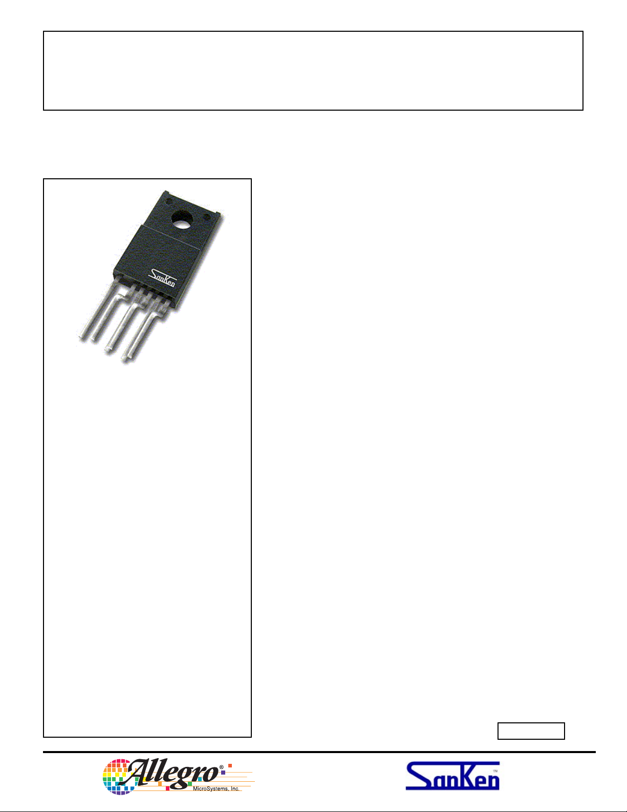
STR-W6753 is provided in a fully molded TO-220-style flangemounted, high power, isolated plastic package.
FEATURES
■ Rugged 650 V Avalanche-Rated MOSFET
Simplified Surge Absorption
No V
■ 1.7 Ω Maximum
■ Two Operational Modes by Automatic Switching:
Quasi-Resonant Mode for Normal Operation
Burst Mode for Standby Operation or Light Loads
■ Automatic or Manually Triggered Burst Standby
Input Power <0.1 W at No Load
■ Low Operating Current (6 mA typ)
Always order by complete part number, e.g., STR-W6753 .
Derating Required
DSS
r
DS(on)
AND BENEFITS
— continued
Data Sheet
Sanken Power Devices
from Allegro MicroSystems
STR-W6753
Universal-Input/58 W Off-Line QuasiResonant Flyback Switching Regulator
FUNCTIONAL BLOCK DIAGRAM
Switching
Regulators
FEATURES AND BENEFITS (cont’d)
■ Auto-Bias Function
Stable Burst Operation Without Generating Interference
■ Internal Off-Timer Circuit
■ Built-In Constant-Voltage Drive
■ Multiple Protections:
Pulse-by-Pulse Overcurrent Protection
Overload Protection with Auto Recovery
Latching Overvoltage Protection
Undervoltage Lockout with Hysteresis
■ RoHS Compliant
2
115 Northeast Cutoff, Box 15036
Worcester, Massachusetts 01615-0036
Copyright © 2005 Allegro MicroSystems, Inc.
STR-W6753
Universal-Input/58 W Off-Line Quasi-
Switching
Resonant Flyback Switching Regulator
Regulators
ELECTRICAL CHARACTERISTICS at TA = +25°C, VCC = 20 V, voltage measurements are referenced to S/GND terminal
(unless otherwise specified).
Limits
Characteristic Symbol Test Conditions Min. Typ. Max. Units
Start-Up Operation
Operation Start Voltage V
Soft-Start Operation Stop Voltage V
Soft-Start Oper. Charging Current I
Operation Stop Voltage V
Circuit Current in Non-Operation I
CC(ON)
SS/OLP
SS/OLP
CC(OFF)
CC(OFF)
Normal Operation
Drain-Source Breakdown Voltage V
(BR)DSS
Drain Leakage Current I
On-State Resistance r
DS(on)
Switching Time t
Circuit Current I
CC(ON)
Oscillation Frequency f
Bottom-Skip Oper. Threshold Volt. V
Quasi-Resonant Oper. Threshold V
OCPBD(BS1)
V
OCPBD(BS2)
OCPBD(TH1)
DSS
osc
Turn-on, VCC = 0 19.9 V 16.3 18.2 19.9 V
1.1 1.2 1.4 V
-390 -550 -710 µA
Turn-off, VCC = 19.9 8 .8 V 8.8 9.7 10.6 V
VCC = 15 V – – 100 µA
ID = 300 µA 650 – – V
VDS = 650 V – – 300 µA
ID = 1.4 A, TJ = +25°C – – 1.7 Ω
f
– – 400 ns
– – 6.0 mA
19 22 25 kHz
-605 -665 -720 mV
-385 -435 -485 mV
280 400 520 mV
V
OCPBD(TH2)
Feedback-Pin Threshold Voltage V
Feedback-Pin Current I
FB(OFF)
FB(ON)
Standby Operation
Standby Operation Start Voltage V
Standby Oper. Start Volt. Interval V
Standby Non-Operation Current I
Feedback-Pin Current I
FB(ON)
Feedback-Pin Threshold Voltage V
Minimum ON Time t
www.allegromicro.com
on(min)
CC(S)
CC
CC(S)
FB(S)
670 800 930 mV
1.32 1.45 1.58 V
600 1000 1400 µA
VCC = 0 12.2 V 10.3 11.1 12.1 V
1.10 1.35 1.65 V
VCC = 10.2 V – 20 56 µA
VCC = 10.2 V – 4.0 14 µA
VCC = 12.2 V 0.55 1.10 1.50 V
0.5 0.8 1.2 µs
continued next page ...
3